

Page 1
Transistor
2SC3929, 2SC3929A
Silicon NPN epitaxial planer type
For low-frequency output amplification
Complementary to 2SA1531 and 2SA1531A
Features
■
●
Low noise voltage NV.
●
High foward current transfer ratio hFE.
●
S-Mini type package, allowing downsizing of the equipment and
automatic insertion through the tape packing and the magazine
packing.
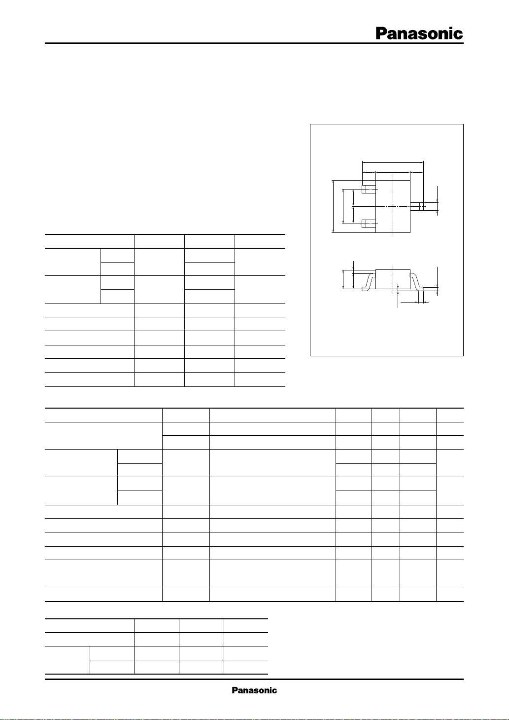
Absolute Maximum Ratings (Ta=25˚C)
■
Parameter
Collector to
base voltage
Collector to
emitter voltage
2SC3929
2SC3929A
2SC3929
2SC3929A
Emitter to base voltage
Peak collector current
Collector current
Collector power dissipation
Junction temperature
Storage temperature
Electrical Characteristics (Ta=25˚C)
■
Parameter
Collector cutoff current
Collector to base
voltage
Collector to emitter
voltage
Emitter to base voltage
Forward current transfer ratio
Collector to emitter saturation voltage
Base to emitter voltage
Noise voltage
Transition frequency
*1
h
Rank classification
FE1
Rank R S T
h
FE
Marking
Symbol
2SC3929 SR SS ST
2SC3929A TR TS TT
Symbol
V
CBO
V
CEO
V
EBO
I
CP
I
C
P
C
T
j
T
stg
Ratings
35
55
35
55
5
100
50
150
150
–55 ~ +150
Symbol
2SC3929
2SC3929A
2SC3929
2SC3929A
I
CBO
I
CEO
V
V
V
h
V
V
NV
f
T
FE
CBO
CEO
EBO
*
CE(sat)
BE
VCB = 10V, IE = 0
VCE = 10V, IB = 0
IC = 10µA, IE = 0
IC = 2mA, IB = 0
IE = 10µA, IC = 0
VCE = 5V, IC = 2mA
IC = 100mA, IB = 10mA
VCE = 1V, IC = 100mA
VCE = 10V, IC = 1mA, GV = 80dB
Rg = 100kΩ, Function = FLAT
VCB = 5V, IE = –2mA, f = 200MHz
180 ~ 360 260 ~ 520 360 ~ 700
Unit
V
V
V
mA
mA
mW
˚C
˚C
Conditions
2.1±0.1
1.25±0.1 0.4250.425
1
1.3±0.10.9±0.1
2.0±0.2
0.650.2 0.65
2
0.7±0.1
0.2±0.1
0 to 0.1
1:Base
2:Emitter EIAJ:SC–70
3:Collector S–Mini Type Package
Marking symbol : S
min
(2SC3929)
(2SC3929A)
T
typ
35
55
35
55
5
180
0.7
80
max
100
1
700
0.6
1
150
3
Unit: mm
–0
+0.1
0.3
–0.05
+0.1
0.15
Unit
nA
µA
V
V
V
V
V
mV
MHz
1
Page 2
Transistor 2SC3929, 2SC3929A
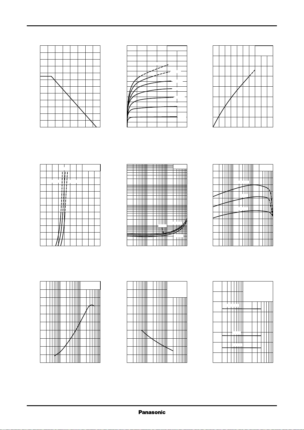
PC — Ta IC — V
240
)
mW
200
(
C
160
120
80
40
Collector power dissipation P
0
0 16040 12080 14020 10060
Ambient temperature Ta (˚C
IC — V
BE
120
100
)
mA
(
80
C
60
40
Collector current I
20
0
02.01.60.4 1.20.8
Base to emitter voltage VBE (V
Ta=75˚C
25˚C
–25˚C
VCE=5V
CE
160
140
)
120
mA
(
C
100
80
60
40
Collector current I
20
0
012108264
)
)
Collector to emitter voltage VCE (V
)
100
V
(
30
CE(sat)
10
3
1
0.3
0.1
0.03
0.01
Collector to emitter saturation voltage V
0.1 1 10 1000.3 3 30
Collector current IC (mA
V
IB=350µA
CE(sat)
— I
25˚C
Ta=25˚C
300µA
250µA
200µA
150µA
100µA
50µA
C
IC/IB=10
Ta=75˚C
–25˚C
)
160
140
)
120
mA
(
C
100
80
60
40
Collector current I
20
0
00.50.40.1 0.30.2
)
720
FE
600
480
360
240
120
Forward current transfer ratio h
0
0.1 1 10 1000.3 3 30
IC — I
B
VCE=5V
Ta=25˚C
Base current IB (mA
hFE — I
C
VCE=5V
Ta=75˚C
25˚C
–25˚C
Collector current IC (mA
)
)
fT — I
500
)
400
MHz
(
T
300
200
100
Transition frequency f
0
– 0.1 –1 –10 –100– 0.3 –3 –30
Emitter current IE (mA
2
E
VCB=5V
Ta=25˚C
)
pF
(
20
16
ob
12
8
4
Collector output capacitance C
0
0.1 1 10 1000.3 3 30
)
Collector to base voltage VCB (V
Cob — V
CB
IE=0
f=1MHz
Ta=25˚C
)
mV
(
Noise voltage NV
)
160
140
120
100
80
60
40
20
0
Collector to emitter voltage VCE (V
NV — V
Rg=100kΩ
1 3 10 30 100
22kΩ
4.7kΩ
CE
IC=1mA
=80dB
G
V
Function=FLAT
)
Page 3

Transistor 2SC3929, 2SC3929A
NV — V
300
Rg=100kΩ
240
)
mV
(
180
120
Noise voltage NV
60
0
1 3 10 30 100
22kΩ
4.7kΩ
CE
IC=1mA
=80dB
G
V
Function=RIAA
Collector to emitter voltage VCE (V
NV — R
160
140
)
120
mV
(
100
80
60
40
Noise voltage NV
20
g
VCE=10V
=80dB
G
V
Function=FLAT
IC=1mA
0.5mA
0.1mA
160
140
)
120
mV
(
100
80
60
40
Noise voltage NV
20
)
300
240
)
mV
(
180
120
Noise voltage NV
60
NV — I
C
VCE=10V
=80dB
G
V
Function=FLAT
Rg=100kΩ
22kΩ
4.7kΩ
0
0.01 0.03 0.1 0.3 1
Collector current IC (mA
NV — R
VCE=10V
=80dB
G
V
Function=RIAA
IC=1mA
)
g
0.5mA
0.1mA
NV — I
C
300
VCE=10V
=80dB
G
V
Function=RIAA
240
)
mV
(
180
120
Noise voltage NV
60
0
0.01 0.03 0.1 0.3 1
Rg=100kΩ
22kΩ
Collector current IC (mA
4.7kΩ
)
0
1 3 10 30 100
Signal source resistance Rg (kΩ
0
1 3 10 30 100
)
Signal source resistance Rg (kΩ
)
3
 Loading...