

Page 1
Inchange Semiconductor Product Specification
Silicon PNP Power Transistors 2SA1387
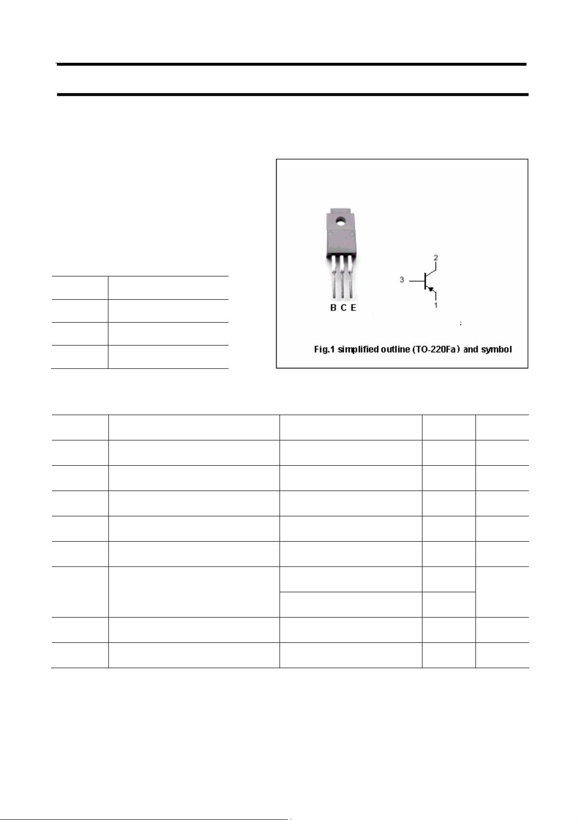
DESCRIPTION ·
·With TO-220Fa package
·Low collector saturation voltage
·High speed switching time
·High DC current gain
APPLICATIONS
·High current switching applications
PINNING
PIN DESCRIPTION
1
2 Collector
3 Base
Emitter
Absolute maximum ratings(Ta=25
SYMBOL PARAMETER CONDITIONS VALUE UNIT
V
CBO
V
CEO
V
EBO
I
C
I
B Base current -1 A
B
P
C
Collector-base voltage Open emitter -60 V
Collector-emitter voltage Open base -50 V
Emitter-base voltage Open collector -7 V
Collector current -5 A
Collector power dissipation
℃)
Ta=25℃ 2
=25℃ 20
T
C
W
T
j
T
stg
Junction temperature 150 ℃
Storage temperature -55~150 ℃
Page 2
Inchange Semiconductor Product Specification
Silicon PNP Power Transistors 2SA1387
CHARACTERISTICS
Tj=25℃ unless otherwise specified
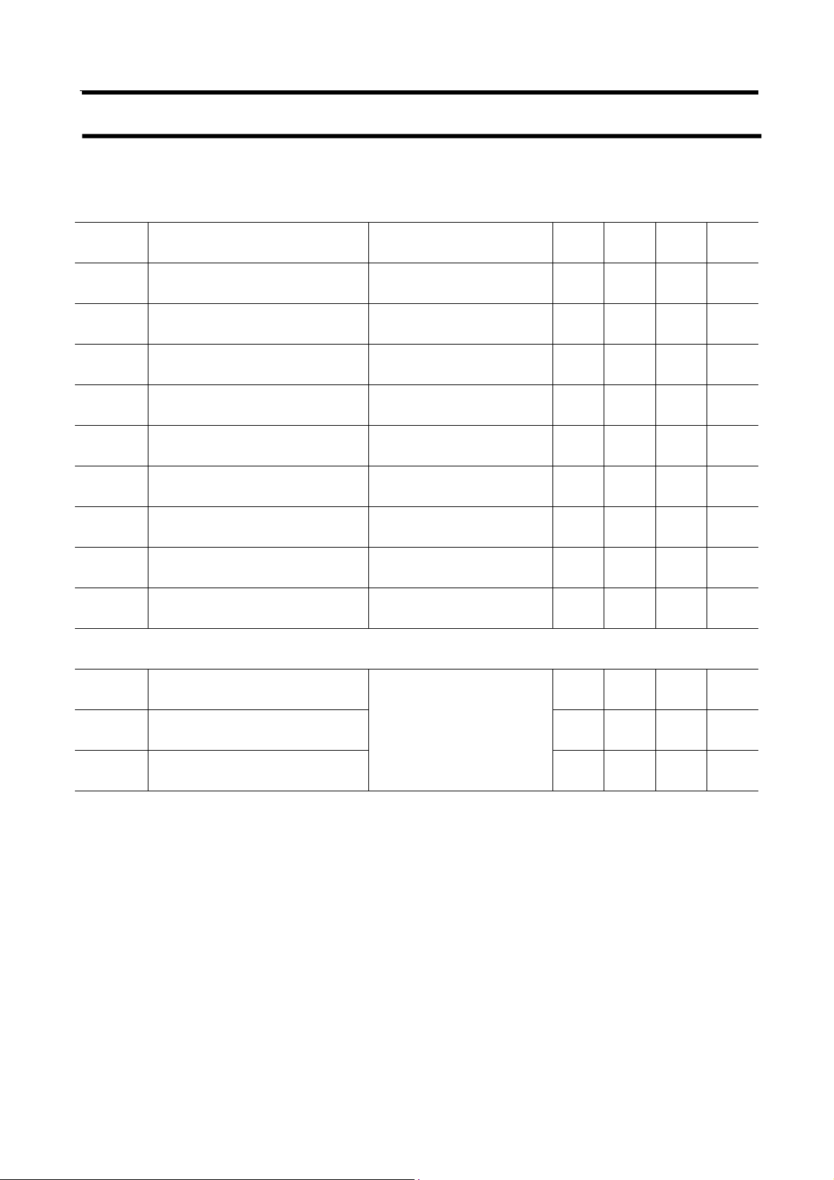
SYMBOL PARAMETER CONDITIONS MIN TYP. MAX UNIT
V
(BR)CEO
V
CEsat
V
BEsat
I
CBO
I
EBO
h
h
C
FE-1
FE-2
f
T
ob
Collector-emitter breakdown voltage IC=-10mA ;IB=0 -50 V
Collector-emitter saturation voltage IC=-3A ;IB=-0.075A B -0.15 -0.4 V
Base-emitter saturation voltage IC=-3A ; IB=-0.075A -0.8 -1.2 V
Collector cut-off current VCB=-50V; IE=0 -1 μA
Emitter cut-off current VEB=-7V; IC=0 -1 μA
DC current gain IC=-1A ; VCE=-1V 150 400
DC current gain IC=-3A ; VCE=-1V 70
Trainsition frequency IC=-1A ; VCE=-4V 80 MHz
Collector output capacitance IE=0; VCE=-10V;f=1MHz 200 pF
Switching times
T
on
t
s
t
f
Turn-on time 0.2 μs
=-IB2=-0.075A
I
Storage time 1.0 μs
Fall time
B1
≈-30V;RL=10Ω
V
CC
0.2 μs
2
Page 3
Inchange Semiconductor Product Specification
Silicon PNP Power Transistors 2SA1387
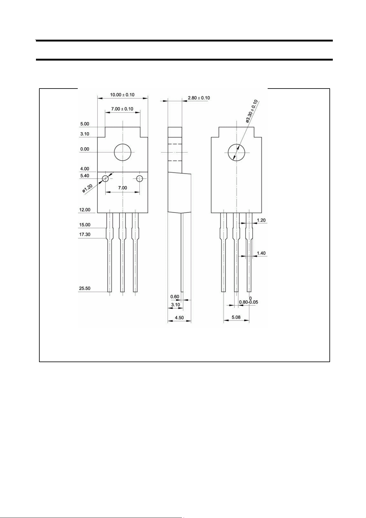
PACKAGE OUTLINE
Fig.2 Outline dimensions (unindicated tolerance:±0.15 mm)
3
Page 4
Inchange Semiconductor Product Specification
Silicon PNP Power Transistors 2SA1387
4
 Loading...