

Page 1
2N6253 - 2N6254 - 2N6371
HIGH POWER SILICON NPN TRANSISTORS
The 2N6253, 2N6254, and 2N6371 are silicon NPN transistors intended for a wide
variety of high-power applications. The construction of these devices renders them
highly resistant to second breakdown over a wide range of operating conditions.
These devices differ in maximum ratings for voltage and power dissipation. All are
supplied in JEDEC TO-3 hermetic stee l packages.
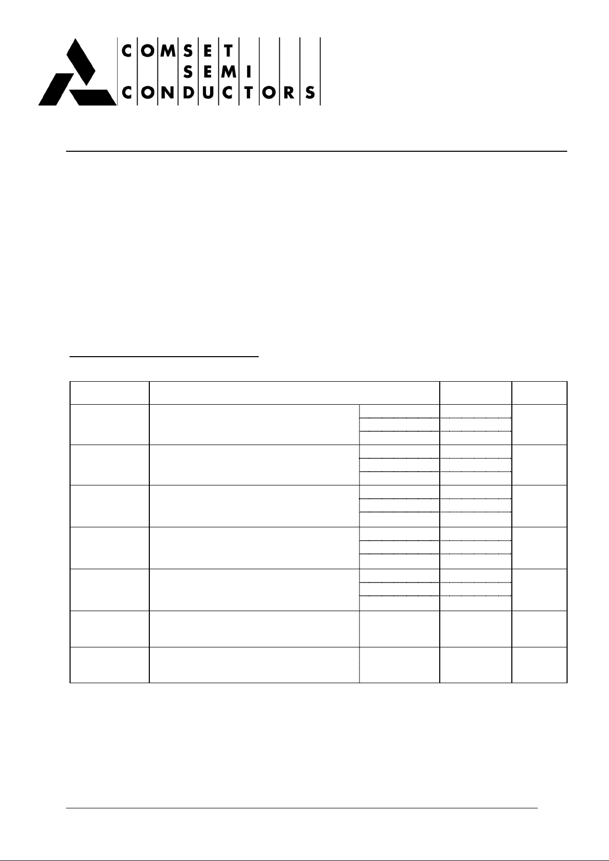
ABSOLUTE MAXIMUM RATINGS
Symbol Ratings Value Unit
V
CEO(SUS)
V
CBO
V
CER(SUS)
V
CEV(SUS)
V
EBO
I
C
I
B
Collector-Emitter Voltage
Collector-Base Voltage (*)
Collector-Emitter Voltage
=100
=-1.5V
Ω
R
BE
Collector-Emitter Voltage
V
BE
Emitter-Base Voltage
Collector Current
Base Current
2N6253
2N6254
2N6371
2N6253
2N6254
2N6371
2N6253
2N6254
2N6371
2N6253
2N6254
2N6371
2N6253
2N6254
2N6371
2N6253
2N6254
2N6371
2N6253
2N6254
2N6371
45
80
40
55
100
50
55
85
45
55
90
50
5
7
5
15
7
V
V
V
V
V
A
A
COMSET SEMICONDUCTORS 1/4
Page 2
2N6253 - 2N6254 - 2N6371
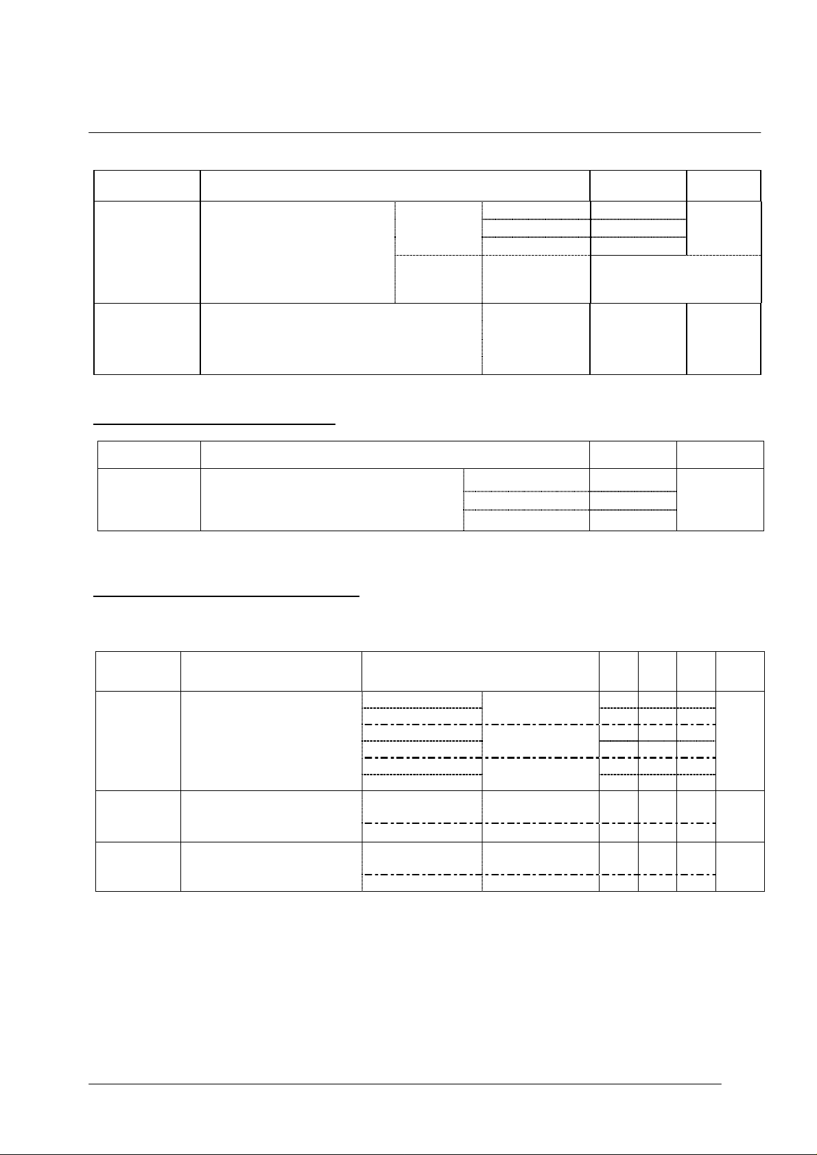
Symbol Ratings Value Unit
2N6253
< 25°C
P
TOT
T
J
T
S
Power Dissipation
> 25°C
Junction Temperature
Storage Temperature
2N6254
2N6371
2N6253
2N6254
2N6371
2N6253
2N6254
2N6371
115
150
117
Derate Linearly to
200°C
-65 to +200 °C
THERMAL CHARACTERISTICS
Symbol Ratings Value Unit
R
thJ-C
Thermal Resistance, Junction to Case
2N6253
2N6254
2N6371
1.5
1.17
1.5
ELECT RICAL CHARACTERISTICS
Watts
°C/W
TC=25°C unless otherwise noted
Symbol Ratings Test Condition(s) Min Typ Mx Unit
V
CE(SAT)
I
CEO
I
EBO
Collector-Emitter Voltage (*)
Collector-Emitter Cutoff
Current
Emitter-Base Cutoff Current
IC=3 A, IB=0.3
IC=15 A, IB=5
IC=5 A, IB=0.5
IC=15 A, IB=3
IC=8 A, IB=0.8
IC=16 A, IB=4
VCE=25 V
VCE=60 V
VEB=-5 V
VEB=-7 V
2N6253
2N6254
2N6371
2N6253
2N6371
2N6254
2N6253
2N6371
2N6254
--1
--4
--0.5
--4
--1.5
--4
--1.5
--1.0
--10
0.5
V
mA
mA
COMSET SEMICONDUCTORS 2/4
Page 3

2N6253 - 2N6254 - 2N6371
Symbol Ratings Test Condition(s) Min Typ Mx Unit
I
CEX
V
CEO(SUS)
V
CER(SUS)
V
CEV(SUS)
V
BE
h
FE
h
fe
Collector Cutoff Current
Collector-Emitter Sustaining
Voltage (*)
Collector-Emitter Sustaining
Voltage (*)
=100
Ω
R
BE
Base-Emitter Voltage (*)
Base-Emitter Voltage (*)
Static Forward Current
transfer ratio (*)
Small Signal Current Gain
VCE=40 V
=-1.5 V
V
BE
VCE=50 V
VBE=-1.5 V
=150°C
C
T
VCE=100 V
=1.5 V
V
BE
VCE=45 V
VBE=-1.5 V
VCE=55 V
=25°C
=-1.5 V
V
BE
C
T
VCE=100 V
=1.5 V
V
BE
IC=0.2 A, IB=0 A
IC=0.2 mA
IC=0.1 A, VBE=-1.5
V
VCE=4 V, IC=3 A
VCE=2 V, IC=5 A
VCE=4 V, IC=16 A
VCE=4 V, IC=3 A
VCE=4 V, IC=15 A
VCE=2 V, IC=5 A
VCE=4 V, IC=15 A
VCE=4 V, IC=8 A
VCE=4 V, IC=16 A
VCE=4 V, IC=1 A,
f=1 kHz
2N6371
2N6253
2N6254
2N6371
2N6253
2N6254
2N6253
2N6254
2N6371
2N6253
2N6254
2N6371
2N6253
2N6254
2N6371
2N6253
2N6254
2N6371
2N6253
2N6254
2N6371
2N6253
2N6254
2N6371
--10
--10
mA
--5.0
--2.0
--2.0
--0.5
45 - 80 - 40 - 55 - -
-
85
45
-
-
55 - 90 - -
50 - -
--1.7
--1.5
--4
20 - 70
3--
20 - 70
5--
15 - 60
4--
10 - - -
V
V
V
V
-
f
T
Transition Frequency
Second Breakdown
I
s/b
Collector Current
tp=1s, non rep.
(*) Pulse Width ≈ 300 µs, Duty Cycle ∠ 2.0%
COMSET SEMICONDUCTORS 3/4
VCE=4 V, IC=1 A
VCE=45 V
VCE=40 V
2N6253
2N6254
2N6371
2N6253
2N6254
2N6371
---
---
800 - -
2.55 - -
1.87 - -
2.9 - -
kHz
A
Page 4

2N6253 - 2N6254 - 2N6371
MECHANICAL DATA C ASE TO- 3
DIMENSIONS
mm inches
A 25,45 1
B 38,8 1,52
C 30,09 1,184
D 17,11 0,67
E 9,78 0,38
G 11,09 0,43
H 8,33 0,32
L 1,62 0,06
M 19,43 0,76
N 1 0,04
P 4,08 0,16
Pin 1 : Base
Pin 2 : Emitter
Case : Collector
Information furnished is believed to be accurate and reliable. However, CS assumes no respons ability
for the consequences of use of such information nor for errors that could appear.
Data are subject to change without notice
COMSET SEMICONDUCTORS 4/4
 Loading...