

Page 1
SILICON PNP SWITCHING TRANSISTORS
■ SGS-THOMS O N PREF ERRE D SA LES TYP E S
■ PNP TRANS IST OR S
APPLICATIONS:
■ LINEAR AND SWITCHING INDUSTRIAL
EQUIPMENT
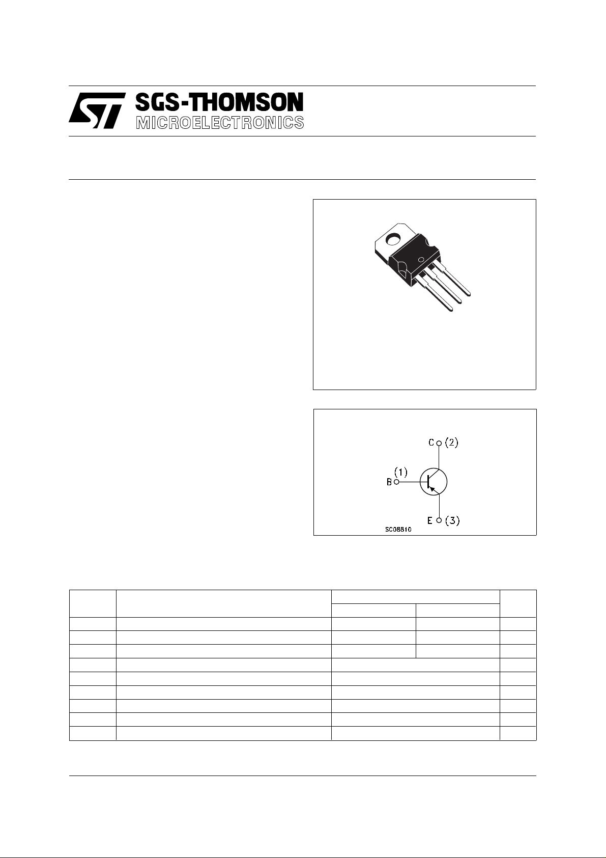
DESCRIPTION
The 2N6107 and 2N6111 are epitaxial-base PNP
silicon transistors in Jedec TO-220 plastic
package. They are intended for a wide variety of
medium power switching and linear applications.
TO-220
2N6107
2N6111
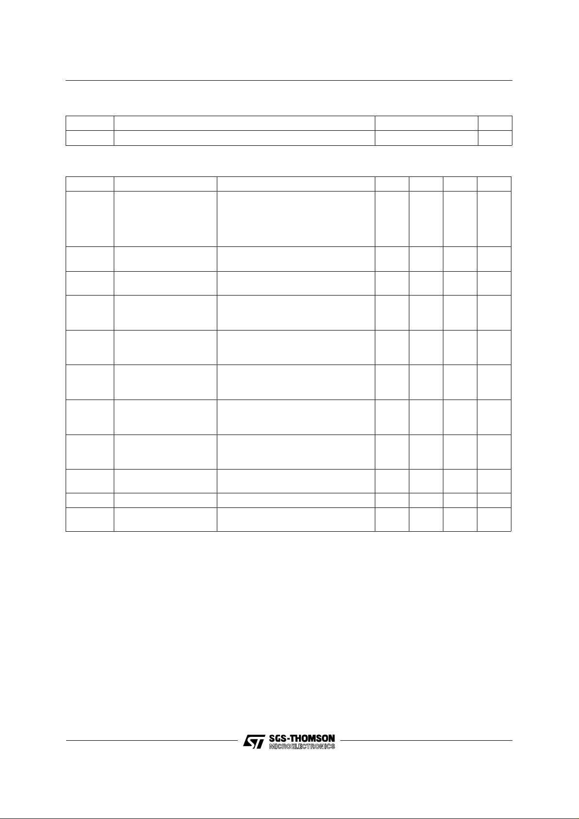
3
2
1
INTERNAL SCHEMATIC DIAGRAM
ABSOL UT E MAXIMU M RATINGS
Symbol Parameter Value Unit
2N6107 2N6111
V
V
V
V
P
T
For PNP devices volt age and current values are negative
Collector-Base Voltage (IE = 0) 80 40 V
CBO
Collector-Emitter Voltage (RBE = 100 Ω)8040V
CEX
Collector-Emitter Voltage (IB = 0) 70 30 V
CEO
Emitter-Base Voltage (IC = 0) 5 V
EBO
Collector Current 7 A
I
C
Base Current 3 A
I
B
Total Dissipation at Tc = 25 oC40W
tot
Storage Temperature -65 to 150
stg
Max. Operating Junction Temperature 150
T
j
o
C
o
C
June 1997
1/4
Page 2
2N6107/2N6111
THERMAL DATA
R
thj-case
R
thj-amb
Thermal Resistance Junction-case Max 3.12
Thermal Resistance Junction-ambient Max 70
o
C/W
o
C/W
ELECTRICAL CHARACTERISTICS (T
= 25 oC unless otherwise specified)
case
Symbol Parameter Test Conditions Min. Typ. Max. Unit
I
CEX
I
CEO
I
EBO
V
CEO(sus)
V
CER(sus)
V
CE(sat)
V
BE(on)
h
h
FE
Collector Cut-off
Current (V
= - 1.5V)
BE
Collector Cut-off
Current (I
= 0)
B
Emitter Cut-off Current
(I
= 0)
C
∗ Collector-emitter
Sustaining Voltage
for 2N6107 V
for 2N6111 V
T
= 150 oC
C
for 2N6107 V
for 2N6111 V
for 2N6107 V
for 2N6111 V
= 5 V 1 mA
V
EB
IC = 0.1 A
for 2N6107
= 80 V
CE
= 40 V
CE
= 70 V
CE
= 30 V
CE
= 60 V
CE
= 20 V
CE
for 2N6111
∗ Collector-emitter
Sustaining Voltage
IC = 0.1 A RBE = 100 Ω
for 2N6107
for 2N6111
∗ Collector-emitter
Saturation Voltage
IC = 3 A IB = 0.3 A for 2N6107
I
= 2 A IB = 0.2 A for 2N6111
C
I
= 7 A IB = 3.0 A
C
∗ Base-emitter Voltage IC = 3 A VCE = 4 V for 2N6107
I
= 2 A VCE = 4 V for 2N6111
C
I
= 7 A VCE = 4 V
C
∗ DC Current Gain IC = 3 A VCE = 4 V for 2N6107
I
= 2 A VCE = 4 V for 2N6111
C
I
= 7 A VCE = 4 V
C
Small Signal Current
fe
IC = 0.5 A VCE = 4 V f = 50 KHz 20
70
30
80
40
30
30
2.3
0.1
0.1
2
2
1
1
1
1
3.5
1.5
1.5
3
150
150
Gain
f
C
Transition-Frequency IC = 0.5 A VCE = 4 V 4 MHz
T
cbo
Collector-base
VCB = 10 V f = 1 MHz 250 pF
Capacitance
∗ Pulsed: Pulse duration = 300 µs, duty cycle 1.5 %.
For PNP types voltage and current values are negative.
For characteristic curves see the bd534 (PNP) series.
mA
mA
mA
mA
mA
mA
V
V
V
V
V
V
V
V
V
V
2/4
Page 3

P011C
TO-220 MECHANICAL DATA
2N6107/2N6111
DIM.
MIN. TYP. MAX. MIN. TYP. MAX.
A 4.40 4.60 0.173 0.181
C 1.23 1.32 0.048 0.051
D 2.40 2.72 0.094 0.107
D1 1.27 0.050
E 0.49 0.70 0.019 0.027
F 0.61 0.88 0.024 0.034
F1 1.14 1.70 0.044 0.067
F2 1.14 1.70 0.044 0.067
G 4.95 5.15 0.194 0.203
G1 2.4 2.7 0.094 0.106
H2 10.0 10.40 0.393 0.409
L2 16.4 0.645
L4 13.0 14.0 0.511 0.551
L5 2.65 2.95 0.104 0.116
L6 15.25 15.75 0.600 0.620
L7 6.2 6.6 0.244 0.260
L9 3.5 3.93 0.137 0.154
DIA. 3.75 3.85 0.147 0.151
mm inch
3/4
Page 4

2N6107/2N6111
Information furnished is believed to be accurate and reliable. However, SGS-THOMSON Microelectronics assumes no responsability for the
consequences of use of such information nor for any infringement of patents or other rights of third parties which may results from its use. No
license is granted by implication or ot h erwise under any patent or patent rights of SGS-THOMSON Microelectronics. Specifi cations mentioned
in this publication are subject to change without notice. This publication sup ersedes and replaces all information previously supplied.
SGS-THOMSON Microelectronics products are not authorized for use as critical components in life support devices or systems without express
written approval of SGS-THOMSON Microelectonics.
© 1997 SGS-THOMSON Microelectronics - Printed in Italy - All Rights Reserved
Australia - Brazil - Canada - China - France - Germany - Hong Kong - Italy - Japan - Korea - Malaysia - Malta - Morocco - The Netherlands -
Singapore - Spain - Sweden - Switzerland - Taiwan - Thailand - United Kingdom - U.S.A
SGS-THOMSON Microelectronics GROUP OF COMPANIES
. . .
4/4
 Loading...