

Page 1
■ SGS-THOMS O N PREF ERRE D SA LES TYP E S
■ NPN TRANSISTOR
APPLICATIONS
■ GENERAL PURPOSE SWITCHING
■ GENER AL PURPOSE AMPLIFIERS
DESCRIPTION
The 2N5681, 2N5682 are high voltage silicon
epitaxial planar NPN transistors in Jedec TO-39
metal case intended for use as drivers for high
power transistors in general purpose, amplifier
and switching applications.
The complementary PNP types are the 2N5679
and 2N5680 respectively.
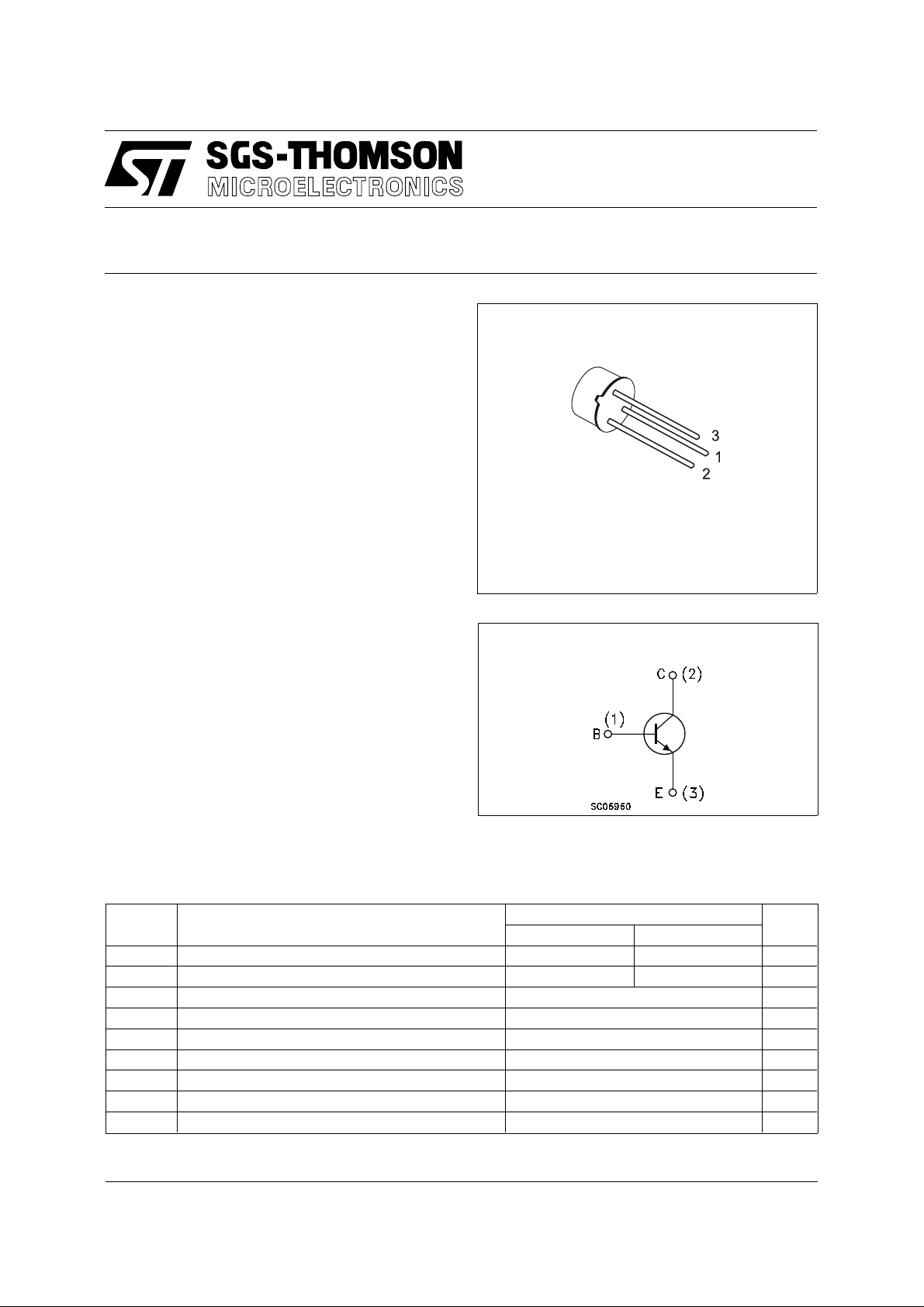
2N5681
2N5682
SILICON NPN TRANSISTORS
TO-39
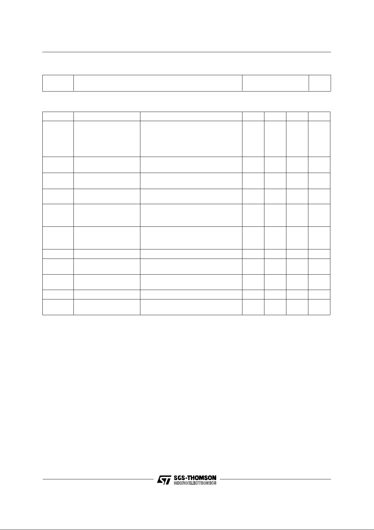
INTERNAL SCHEMATIC DIAGRAM
ABSOL UT E MAXIMU M RATINGS
Symbol Parameter Value Unit
2N5680 2N5682
V
V
V
P
P
T
Collector-Base Voltage (IE = 0) 100 120 V
CBO
Collector-Emitter Voltage (IB = 0) 100 120 V
CEO
Emitter-Base Voltage (IC = 0) 4 V
EBO
Collector Current 1 A
I
C
Base Current 0.5 A
I
B
Total Dissipation at Tc ≤ 25 oC10W
tot
Total Dissipation at T
tot
Storage Temperature -65 to 200
stg
Max. Operating Junction Temperature 200
T
j
≤ 50 oC1W
amb
o
C
o
C
July 1997
1/4
Page 2
2N5681 / 2N5682
THERMAL DATA
R
thj-case
R
thj-amb
Thermal Resistance Junction-case Max
Thermal Resistance Junction-ambient Max
17.5
175
o
C/W
o
C/W
ELECTRICAL CHARACTERISTICS (T
= 25 oC unless otherwise specified)
case
Symbol Parameter Test Conditions Min. Typ. Max. Unit
I
CEV
I
CBO
I
CEO
I
EBO
V
CEO(sus)
V
CE(sat)
V
h
h
BE
FE
Collector Cut-off
Current (V
= -1.5V)
BE
Collector Cut-off
Current (I
= 0)
E
Collector Cut-off
Current (I
= 0)
B
Emitter Cut-off Current
(I
= 0)
C
∗ Collector-Emitter
Sustaining Voltage
∗ Collector-Emitter
Saturation Voltage
for 2N5681 V
for 2N5682 V
T
= 150 oC
c
for 2N5681 V
for 2N5682 V
for 2N5681 V
for 2N5682 V
for 2N5681 V
for 2N5682 V
= 4 V 1 µA
V
EB
IC = 10 mA
for 2N5681
for 2N5682
IC = 250 mA IB = 25 mA
I
= 500 mA IB = 50 mA
C
I
= 1 A IB = 200 mA
C
= 100 V
CE
= 120 V
CE
= 100 V
CE
= 120 V
CE
= 100 V
CB
= 120 V
CB
= 70 V
CB
= 80 V
CB
1
1
1
1
1
1
10
10
100
120
0.6
1
2
∗ Base-Emitter Voltage IC = 250 mA VCE = 2 V 1 V
∗ DC Current Gain IC = 250 mA VCE = 2 V
I
= 1 A VCE = 2 V
C
Small Signal Current
fe
IC = 0.2 A VCE = 1.5 V f = 1KHz 40
40
150
5
Gain
f
C
CBO
Transition frequency IC = 100 mA VCE = 10 V f =10MHz 30 MHz
T
Collector Base
IE = 0 VCB = 20 V f = 1MHz 50 pF
Capacitance
∗ Pulsed: Pulse duration = 300 µs, duty cycle 1.5 %
µA
µA
µA
µA
µA
µA
µA
µA
V
V
V
V
V
2/4
Page 3

TO-39 MECHANICAL DATA
2N5681 / 2N5682
DIM.
MIN. TYP. MAX. MIN. TYP. MAX.
A 12.7 0.500
B0.490.019
D6.60.260
E8.50.334
F9.40.370
G 5.08 0.200
H1.20.047
I0.90.035
L45
mm inch
o
(typ.)
H
G
D A
I
E
F
L
B
P008B
3/4
Page 4

2N5681 / 2N5682
Information furnished is believed to be accurate and reliable. However, SGS-THOMSON Microelectronics assumes no responsability for the
consequences of use of such information nor for any infringement of patents or other rights of third parties which may results from its use. No
license is granted by implication or ot h erwise under any patent or patent rights of SGS-THOMSON Microelectronics. Specifi cations mentioned
in this publication are subject to change without notice. This publication sup ersedes and replaces all information previously supplied.
SGS-THOMSON Microelectronics products are not authorized for use as critical components in life support devices or systems without express
written approval of SGS-THOMSON Microelectonics.
© 1997 SGS-THOMSON Microelectronics - Printed in Italy - All Rights Reserved
Australia - Brazil - Canada - China - France - Germany - Hong Kong - Italy - Japan - Korea - Malaysia - Malta - Morocco - The Netherlands -
Singapore - Spain - Sweden - Switzerland - Taiwan - Thailand - United Kingdom - U.S.A
SGS-THOMSON Microelectronics GROUP OF COMPANIES
. . .
4/4
 Loading...