

Page 1
SMALL SIGNAL NPN TRANSISTORS
■ SILICON EPI TAX IA L PLANAR N PN
TRANSISTORS
■ MEDIUM POWER AMPLIFIER
■ PNP COMPLEMENT S ARE 2N5322 AN D
2N5323
DESCRIPTION
The 2N5320 and 2N5321 are silicon epitaxial
planar NPN transistors in Jedec TO-39 metal
case. They are especially intended for
high-voltage medium power application in
industrial and commercial equipments.
The complementary PNP types are respectively
the 2N5322 and 2N5323
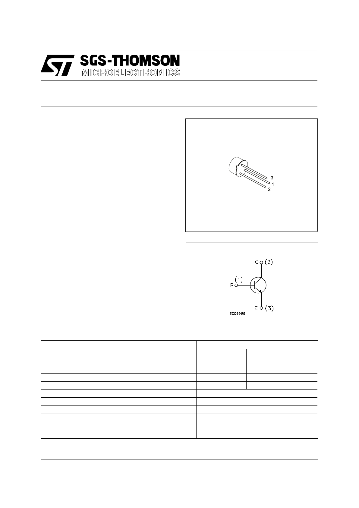
2N5320
2N5321
TO-39
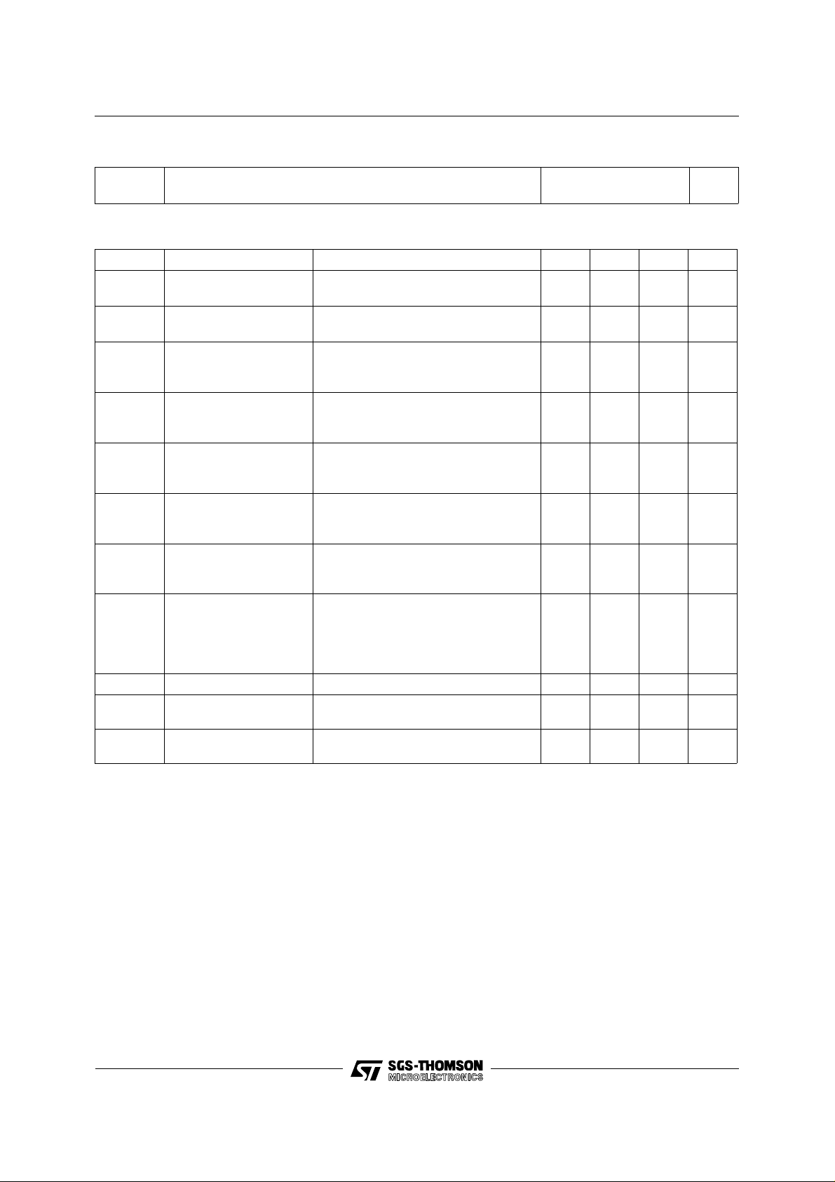
INTERNAL SCHEMATIC DIAGRAM
ABSOL UT E MAXIMU M RATINGS
Symbol Parameter Value Unit
2N5320 2N5321
V
V
V
V
I
P
P
T
stg
Collector-Base Voltage (IE = 0) 100 75 V
CBO
Collector-Emitter Voltage (VBE = 1.5V) 100 75 V
CEV
Collector-Emitter Voltage (IB = 0) 75 50 V
CEO
Emitter-Base Voltage (IC = 0) 6 5 V
EBO
Collector Current 1.2 A
I
C
Collector Peak Current 2 A
CM
Base Current 1 A
I
B
Total Dissipation at T
tot
Total Dissipation at Tc = 25 oC10W
tot
, TjStorage and Junction Temperature -65 to 200
= 25 oC1W
amb
o
C
June 1997
1/4
Page 2
2N5320/2N5321
THERMAL DATA
R
thj-case
R
thj-amb
Thermal Resistance Junction-Case Max
Thermal Resistance Junction-Ambient Max
17.5
175
o
C/W
o
C/W
ELECTRICAL CHARACTERISTICS (T
= 25 oC unless otherwise specified)
case
Symbol Parameter Test Conditions Min. Typ. Max. Unit
I
CBO
I
EBO
V
(BR)CEV
V
(BR)CEO
V
(BR)EBO
V
CE(sat)
V
h
BE
FE
Collector Cut-off
Current (I
= 0)
E
Collector Cut-off
Current (I
= 0)
C
Collector-Emitter
Breakdown Voltage
(V
= 1.5V)
BE
∗ Collector-Emitter
Breakdown Voltage
(I
= 0)
B
Emitter-Base
Breakdown Voltage
(I
= 0)
C
∗ Collector-Emitter
Saturation Voltage
= 80 V for 2N5320
V
CB
V
= 60 V for 2N5321
CB
= 5 V for 2N5320
V
EB
V
= 4 V for 2N5321
EB
= 100 µA
I
C
for 2N5320
for 2N5321
I
= 10 mA
C
for 2N5320
for 2N5321
= 100 µA
I
E
for 2N5320
for 2N5321
IC = 500 mA IB = 50 mA
for 2N5320
for 2N5321
∗ Base-Emitter Voltage IC = 500 mA VCE = 4 V
for 2N5320
for 2N5321
∗ DC Current Gain for 2N5320
I
= 500 mA VCE = 4 V
C
I
= 1 A VCE = 2 V
C
100
75
75
50
6
5
30
10
0.5
5
0.1
0.5
0.5
0.8
1.1
1.4
130
for 2N5321
I
f
t
Transition Frequency IC = 50 mA VCE = 4 V f = 10 MHz 50 MHz
T
Turn-on Time IC = 500 mA VCC = 30 V
on
I
t
Turn-off Time IC = 500 mA VCC = 30 V
off
I
∗ Pulsed: Pulse duration = 300 µs, duty cycle = 1 %
= 500 mA VCE = 4 V
C
= 50 mA
B1
= -IB2 = 50 mA
B1
40
250
80 ns
800 ns
µA
µA
µA
µA
V
V
V
V
V
V
V
V
V
V
2/4
Page 3

TO-39 MECHANICAL DATA
2N5320/2N5321
DIM.
MIN. TYP. MAX. MIN. TYP. MAX.
A 12.7 0.500
B0.490.019
D6.60.260
E8.50.334
F9.40.370
G 5.08 0.200
H1.20.047
I0.90.035
L45
mm inch
o
(typ.)
H
G
D A
I
E
F
L
B
P008B
3/4
Page 4

2N5320/2N5321
Information furnished is believed to be accurate and reliable. However, SGS-THOMSON Microelectronics assumes no responsability for the
consequences of use of such information nor for any infringement of pat e nts or ot her rights o f third partie s which may results from its use. No
license is granted by implication or otherwise under any patent or patent rights of SG S-THOMSON Microelectroni cs. Specifications ment ioned
in this publication are subject to cha nge wi t hout n o tice. This p u bli ca t ion sup e rsed e s and r epla ces al l inf ormat i on pr ev io us ly supplied.
SGS-THOMSON Microelectronics products are not auth orized for use as critical components in life support devices or systems without express
written approval of SGS-THOM SO N M icroele cton ics.
© 1997 SGS-THOMSON Microelectronics - Printed in Ita ly - All Rig hts Rese rved
Australia - Brazil - Canada - China - France - Germany - Hong Kong - Italy - Japan - Korea - Malaysia - Malta - Morocco - The Netherlands -
Singapore - Spain - Sweden - Switzerland - Taiwan - Thailand - United Kingdom - U.S.A
SGS-THOMSON Microelectronics GROUP OF COMPANIES
.
4/4
 Loading...