

Page 1
Discrete POWER & Signal
Technologies
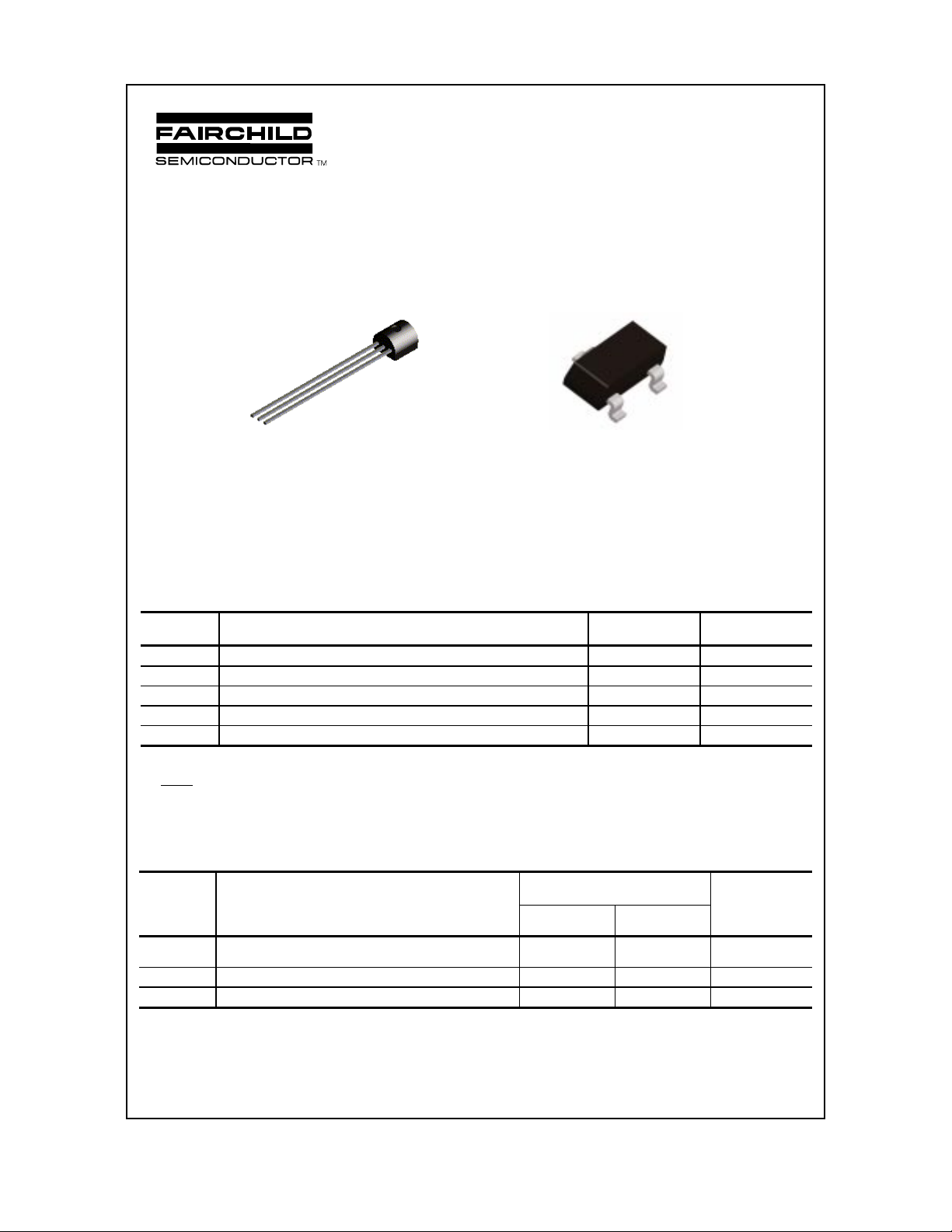
2N5086 / MMBT5086 / 2N5087 / MMBT5087
2N5086
2N5087
C
B
E
TO-92
MMBT5086
MMBT5087
C
SOT-23
Mark: 2P / 2Q
B
E
PNP General Purpose Amplifier
This device is designed for low level, high gain, low noise general
purpose amplifier applications at collector currents to 50 mA.
Sourced from Process 62.
Absolute Maximum Ratings* TA = 25°C unless otherwise noted
Symbol Parameter Value Units
V
CEO
V
CBO
V
EBO
I
C
TJ, T
stg
*These ratings are limiting values above which the serviceability of any semiconductor device may be impaired.
NOTES:
1) These ratings are based on a maximum junction temperature of 150 degrees C.
2) These are steady state limits. The factory should be consulted on applications involving pulsed or low duty cycle operations.
Collector-Emitter Voltage 50 V
Collector-Base Voltage 50 V
Emitter-Base Voltage 5.0 V
Collector Current - Continuous 100 mA
Operating and Storage Junction Temperature Range -55 to +150
°
C
Thermal Characteristics TA= 25°C unless otherwise noted
Symbol Characteristic Max Units
P
D
R
θ
JC
R
θ
JA
Total Device Dissipation
Derate above 25°C
Thermal Resist ance, Junction to Case 83.3
Thermal Resist ance, Junction to Ambient 200 357
*Device mounted on FR-4 PCB 1.6" X 1.6" X 0.06."
ã 1997 Fairchild Semiconductor Corporation
2N5086
2N5086
625
5.0
*MM BT5086
*MM BT5087
350
2.8
mW
mW/°C
C/W
°
C/W
°
Page 2
(BR)
(BR)
PNP General Purpose Amplifier
(continued)
Electrical Characteristics TA= 25°C unless otherwise noted
Symbol Parameter Test Conditions Min Max Units
OFF CHARACTERISTICS
V
CEO
V
CBO
I
CBO
I
EBO
ON CHARACTERISTICS
h
FE
V
sat
CE(
V
BE(on)
Collector-Emitte r Breakdown Voltage* IC = 1.0 mA, IB = 0 50 V
Collector-Base Breakdown Voltag e
I
= 100 µA, IE = 0
C
50 V
Collector Cutoff Current VCB = 10 V, IE = 0
V
= 35 V, IE = 0
CB
Emitter Cutoff Current VEB = 3.0 V, IC = 0 50 nA
DC Current Gain
I
= 100 µA, VCE = 5.0 V
C
2N5086
2N5087
I
= 1.0 mA, VCE = 5.0 V
C
2N5086
2N5087
I
= 10 mA, VCE = 5.0 V
C
2N5086
2N5087
Collector-Emitte r Saturation Voltage IC = 10 mA, IB = 1.0 mA 0.3 V
)
150
250
150
250
150
250
Base-Emitter On Voltage IC = 1.0 mA, VCE = 5.0 V 0.85 V
10
50
500
800
nA
nA
2N5086 / MMBT5086 / 2N5087 / MMBT5087
SMALL SIGNAL CHARACTERISTICS
f
T
C
cb
h
fe
NF Noise Figure
Current Gain - Band width Product
I
= 500 µA,V
C
Collector-Base Capacitance VCB = 5.0 V, I
Small-Si gnal Current Gain IC = 1.0 mA, V
f = 1.0 kHz
I
= 100 µA, VCE = 5.0 V,
C
R
= 3.0 kΩ, f = 1.0 kHz
S
I
= 20 µA, VCE = 5.0 V,
C
R
= 10 kΩ,
S
f = 10 Hz to 15.7 kHz
= 5.0 V,f = 20 MHz
CE
= 0, f = 100 kHz 4.0 pF
E
= 5.0,
2N5086
CE
2N5087
2N5086
2N5087
2N5086
2N5087
40 MHz
150
250
600
900
3.0
2.0
3.0
2.0
*Pulse Test: Pulse Width £ 300 ms, Duty Cycle £ 2.0%
Spice Model
PNP (Is=6.734f Xti=3 Eg=1.11 Vaf=45.7 Bf=254.1 Ne=1.741 Ise=6.734f Ikf=.1962 Xtb=1.5 Br=2.683 Nc=2
Isc=0 Ikr=0 Rc=1.67 Cjc=6.2p Mjc=.301 Vjc=.75 Fc=.5 Cje=7.5p Mje=.2861 Vje=.75 Tr=10.1n Tf=467.8p
Itf=.17 Vtf=5 Xtf=8 Rb=10)
dB
dB
dB
dB
Page 3

Typical Characteristics
2N5086 / MMBT5086 / 2N5087 / MMBT5087
PNP General Purpose Amplifier
(continued)
Typical Pulsed Current Gain
vs Collector Current
350
300
125° C
250
200
25 °C
150
100
- 40 °C
50
0.01 0.03 0.1 0.3 1 3 10 30 100
FE
h - TYPICAL PULSED CURRENT GAIN
I - COLLECTOR C URRENT (mA)
C
V = 5V
CB
Base-Emitter Saturation
Voltage vs Collector Current
1
0.8
0.6
0.4
0.2
0
BESAT
V - BASE EMITTER VOLTAGE (V)
- 40 ºC
25 °C
125 ºC
= 10
β
0.1 1 10 50
I - COLLECTOR CURRENT (mA)
C
Collector-Emitter Saturation
Voltage vs Collector Current
V - COLLECTOR EMITTER VOLTAGE (V)
0.3
0.25
0.2
0.15
0.1
0.05
0
CESAT
= 10
β
25 °C
125 ºC
- 40 ºC
0.1 1 10
I - COLLECTOR CURRENT (mA)
C
Base Emitter ON Voltage vs
Collector Current
1
0.8
- 40 ºC
0.6
0.4
0.2
0
0.1 1 10 25
BEON
V - BASE EMITTER ON VOLTAGE (V)
25 °C
125 ºC
V = 5V
CE
I - COLLECTOR CURRENT (mA)
C
Collector-Cutoff Current
vs. Ambient Temperature
100
V = 40V
CB
10
1
0.1
CBO
0.01
I - COLLECTOR CURRENT (nA)
25 50 75 100 125
T - AMBIENT TEMPER ATURE ( C)
A
º
Input and Output Capacitance
vs Reverse Bias Voltage
20
16
12
8
CAPACITANCE (pF)
4
0
048121620
C
ibo
REVERSE BIAS VOLTAGE (V)
f = 1 MHz
C
obo
Page 4

Typical Characteristics (continued)
0
2N5086 / MMBT5086 / 2N5087 / MMBT5087
PNP General Purpose Amplifier
(continued)
Gain Bandwidth Product
vs Collector Current
350
V = 5V
CE
300
250
200
150
100
50
0
0.1 1 10 100
T
f - GAIN BANDWIDTH PRODUCT (MHz)
I - COLLECTOR CURRENT (mA )
C
Wideband Noise Frequency
vs Source Resistance
8
6
I = 10 µA
C
4
I = 100 µA
C
2
NF - NOISE FIGURE (dB)
0
1,000 2,000 5,000 10,000 20,000 50,000 100,000
R - SOURCE RESISTANCE ( )
S
V = 5V
CE
BANDWIDTH = 15.7 kHz
Ω
Noise Figure vs Frequency
5
4
3
I = - 250 µA, R = 5.0 k
C
2
1
NF - NOISE FIGURE (dB)
0
100 1000 10000 100000
I = - 500 µA, R = 1.0 k
C
I = - 20 µA, R = 10 k
C
S
S
S
f - FREQUENCY (Hz)
Power Dissipation vs
Ambient Temperature
625
TO-92
500
375
SOT-23
250
125
D
P - POWER DISSIPATION (W)
0
0 25 50 75 100 125 150
TEMPERATURE ( C)
o
Ω
Ω
Ω
V = 5V
CE
Equivalent Input Noise Current
√
10
5
2
1
0.5
0.2
0.1
0.001 0.01 0.1 1
2
n
i - EQUIVALENT INPUT NOISE CURRENT (pA/ Hz)
√
vs Collector Current
V = - 5.0V
CE
i , f = 100 Hz
n
i , f = 1.0 kHz
n
i , f = 10 kHz
n
I - COLLECTOR CURRENT (mA)
C
Equivalent Input Noise Voltage
√
0.1
µ
0.05
0.02
0.01
0.005
0.002
0.001
0.001 0.01 0.1 1
2
n
e - EQUIVALENT INPUT NOISE VOLTAGE ( V/ Hz)
√
vs Collector Current
V = - 5.0V
CE
e , f = 100 Hz
n
e , f = 1.0 kHz
n
I - COLLECTOR CURRENT (mA)
C
e , f = 10 kHz
n
Page 5

Typical Characteristics (continued)
2N5086 / MMBT5086 / 2N5087 / MMBT5087
PNP General Purpose Amplifier
(continued)
Contours of Constant
Narrow Band Noise Figure
1,000,000
Ω
100,000
10,000
1,000
V = - 5V
S
R - SOURCE RESISTANCE ( )
f = 10 kHz
BANDWIDTH = 1.5 kHz
100
0.001 0.01 0.1 1
1.0 dB
4.0 dB
6.0 dB
10 dB
CE
I - COLLECTOR CURRENT (mA)
C
Contours of Constant
Narrow Band Noise Figu re
1,000,000
Ω
100,000
10,000
1,000
S
R - SOURCE RESISTANCE ( )
100
0.001 0.01 0.1 1
4.0 dB
6.0 dB
10 dB
I - COLLECTOR CURRENT (mA)
C
10 dB
6.0 dB
4.0 dB
V = - 5V
CE
f = 1.0 kHz
BANDWIDTH = 150 Hz
4.0 dB
2.0 dB
10 dB
6.0 dB
Contours of Constant
Narrow Band Noise Figure
1,000,000
Ω
100,000
10,000
1,000
S
R - SOURCE RESISTANCE ( )
100
0.001 0.01 0.1 1
5.0 dB
8.0 dB
12 dB
I - COLLECTOR CURRENT (mA)
C
5.0 dB
3.0 dB
12 dB
8.0 dB
V = - 5V
CE
f = 100 Hz
BANDWIDTH = 15 Hz
Contours of Constant
Narrow Band Noise Figure
10,000
Ω
5,000
2,000
1,000
500
200
S
R - SOURCE RESISTANCE ( )
100
0.01 0.1 1 10
4.0 dB
6.0 dB
V = - 5V
CE
f = 10 MHz
BANDWIDTH
= - 2 kHz
I - COLLECTOR CURRENT (mA)
C
2.0 dB
4.0 dB
6.0 dB
Page 6

TRADEMARKS
The following are registered and unregistered trademarks Fairchild Semiconductor owns or is authorized to use and is
not intended to be an exhaustive list of all such trademarks.
ACEx™
CoolFET™
CROSSVOLT™
E2CMOS
TM
FACT™
FACT Quiet Series™
®
FAST
FASTr™
GTO™
HiSeC™
ISOPLANAR™
MICROWIRE™
POP™
PowerTrench™
QS™
Quiet Series™
SuperSOT™-3
SuperSOT™-6
SuperSOT™-8
TinyLogic™
DISCLAIMER
FAIRCHILD SEMICONDUCTOR RESERVES THE RIGHT TO MAKE CHANGES WITHOUT FURTHER
NOTICE TO ANY PRODUCTS HEREIN TO IMPROVE RELIABILITY, FUNCTION OR DESIGN. FAIRCHILD
DOES NOT ASSUME ANY LIABILITY ARISING OUT OF THE APPLICATION OR USE OF ANY PRODUCT
OR CIRCUIT DESCRIBED HEREIN; NEITHER DOES IT CONVEY ANY LICENSE UNDER ITS PATENT
RIGHTS, NOR THE RIGHTS OF OTHERS.
LIFE SUPPORT POLICY
FAIRCHILD’S PRODUCTS ARE NOT AUTHORIZED FOR USE AS CRITICAL COMPONENTS IN LIFE SUPPORT
DEVICES OR SYSTEMS WITHOUT THE EXPRESS WRITTEN APPROVAL OF FAIRCHILD SEMICONDUCTOR CORPORATION.
As used herein:
1. Life support devices or systems are devices or
systems which, (a) are intended for surgical implant into
the body, or (b) support or sustain life, or (c) whose
failure to perform when properly used in accordance
with instructions for use provided in the labeling, can be
reasonably expected to result in significant injury to the
user.
2. A critical component is any component of a life
support device or system whose failure to perform can
be reasonably expected to cause the failure of the life
support device or system, or to affect its safety or
effectiveness.
PRODUCT STATUS DEFINITIONS
Definition of Terms
Datasheet Identification Product Status Definition
Advance Information
Preliminary
No Identification Needed
Obsolete
Formative or
In Design
First Production
Full Production
Not In Production
This datasheet contains the design specifications for
product development. Specifications may change in
any manner without notice.
This datasheet contains preliminary data, and
supplementary data will be published at a later date.
Fairchild Semiconductor reserves the right to make
changes at any time without notice in order to improve
design.
This datasheet contains final specifications. Fairchild
Semiconductor reserves the right to make changes at
any time without notice in order to improve design.
This datasheet contains specifications on a product
that has been discontinued by Fairchild semiconductor.
The datasheet is printed for reference information only.
 Loading...