

Page 1
The documentation and process
INCH-POUND
conversion measures necessary to
comply with this revision shall be
completed by 31 November 2000.
MIL-PRF-19500/376E
31 August 2000
SUPERSEDING
MIL-PRF-19500/376D
21 August 1998
PERFORMANCE SPECIFICATION
SEMICONDUCTOR DEVICE, TRANSISTOR, NPN, SILICON, LOW-POWER
TYPES 2N2484, 2N2484UA, 2N2484UB, JAN, JANTX, JANTXV, JANS, JANHC, AND JANKC
This specification is approved for use by all Departments
and Agencies of the Department of Defense.
1. SCOPE
1.1 Scope. This specification covers the performance requirements for NPN, silicon, low-power transistors.
Four levels of product assurance is provided for each device type as specified in MIL-PRF-19500. Two levels of
product assurance are provided for die.
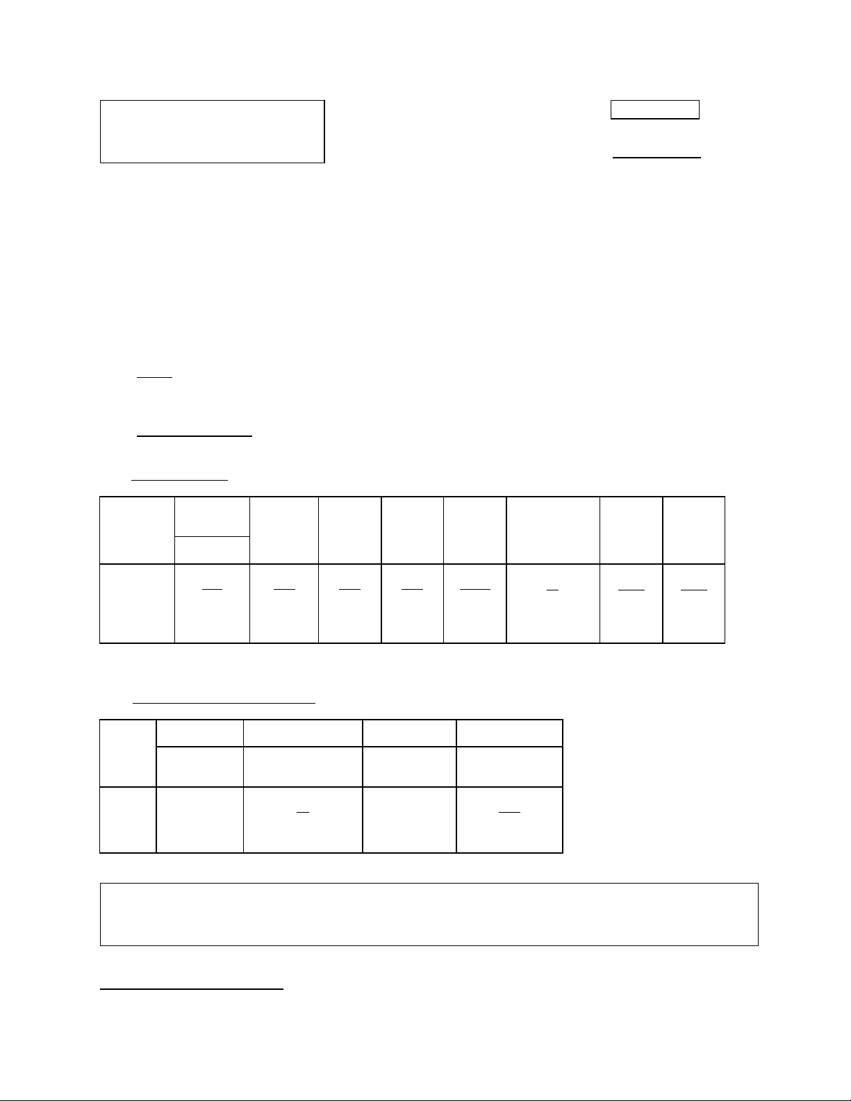
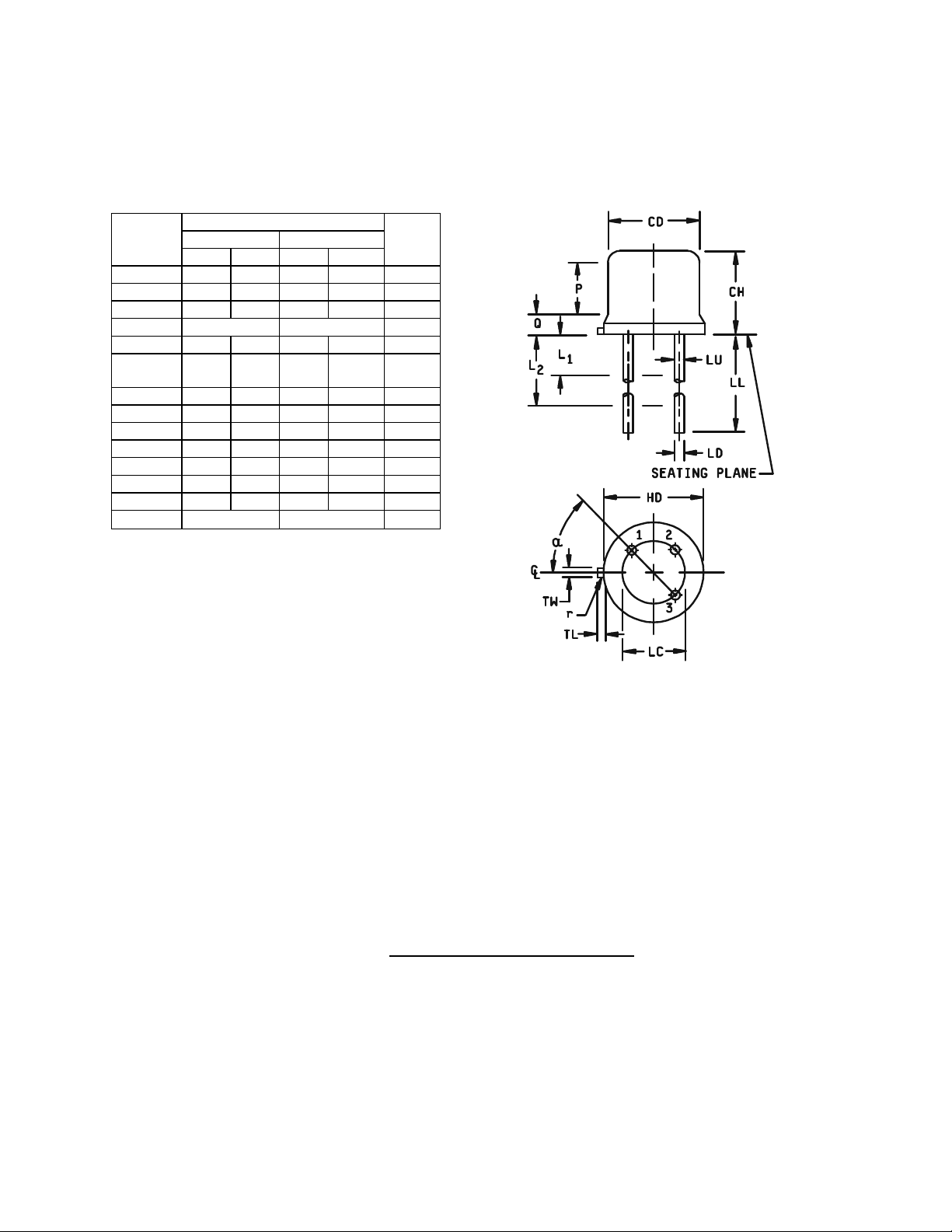
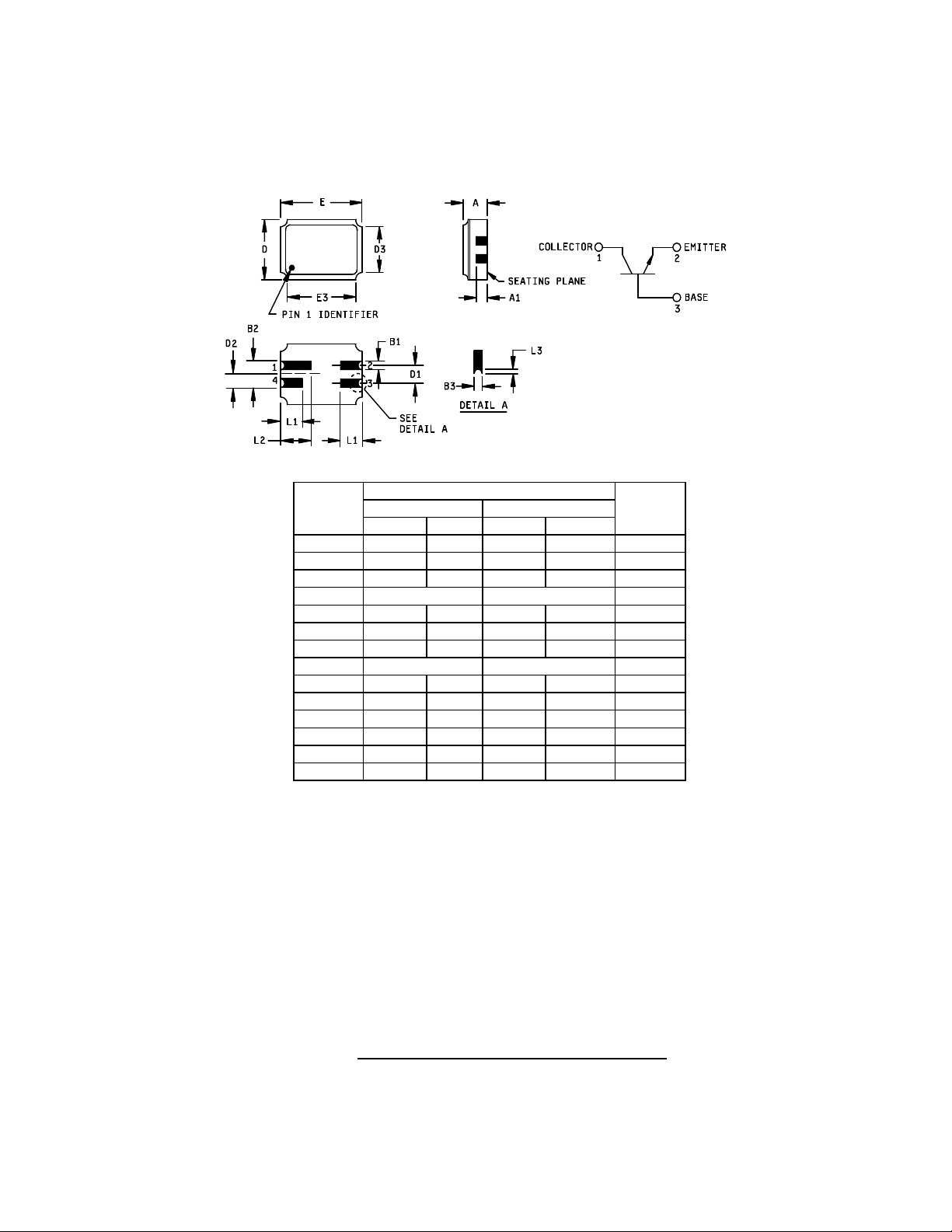
1.2 Physical dimensions. See figure 1 (similar to T0-18), figures 2 and 3 (surface mount case outlines UA and
UB), and figures 4 and 5 (die).
1.3 Maximum ratings.
Types
2N2484 500 (1) 60 6 60 50 -65 to +200 325 146
2N2484UA 650 (2) 60 6 60 50 -65 to +200 210 160
2N2484UB 500 (1) 60 6 60 50 -65 to +200 325 146
P
T
TA = +25°C
mW V dc V dc V dc mA dc
V
CBO
V
EBO
V
CEO
I
C
TJ and T
STG
°C °C/W °C/W
R
θJA
R
θJC
(1) Derate linearly at 3.08 mW/°C above TA = +37.5°C
(2) Derate linearly at 4.76 mW/°C above TA = +63.5°C.
1.4 Primary electrical characteristics.
Limits
Min
Max
h
fe
VCE = 5 V dc
IC = 1 mA dc
f = 1 kHz
250
900
C
obo
IE = 0
VCB = 5 V dc
100 kHz ≤ f ≤ 1 MHz
pF
5.0
|hfe|2 V
IC = 500 µA dc
VCE = 5 V dc
f = 30 MHz
2.0
7.0
(1)
CE(sat)
IC = 1.0 mA dc
IB = 0.1 mA dc
V dc
0.3
(1) Pulsed (see 4.5.1).
Beneficial comments (recommendations, additions, deletions) and any pertinent data which may be of use in
improving this document should be addressed to: Defense Supply Center, Columbus, ATTN: DSCC/VAC,
Post Office Box 3990, Columbus, OH 43216-5000, by using the Standardization Document Improvement Proposal
(DD Form 1426) appearing at the end of this document or by letter.
AMSC N/A FSC 5961
DISTRIBUTION STATEMENT A. Approved for public release; distribution is unlimited.
Page 2
MIL-PRF-19500/376E
Dimensions
Symbol Inches Millimeters Note
Min Max Min Max
CD .178 .195 4.52 4.95
CH .170 .210 4.32 5.33
HD .209 .230 5.31 5.84
LC .100 TP 2.54 TP 6
LD .016 .021 0.41 0.53 7,8
LL .500 .750 12.7019.05 7,8
LU .016 .019 0.41 0.48 7,8
L1 --- .050 --- 1.27 7,8
L2 .250 --- 6.35 --- 7,8
Q --- .040 --- 0.86 5
TL .028 .048 0.71 1.22 3,4
TW .036 .046 0.91 1.17 3
r --- .010 --- 0.25 10
α 45° TP 45° TP
6
NOTES:
1. Dimension are in inches.
2. Metric equivalents are given for general information only.
3. Beyond r (radius) maximum, TW shall be held for a minimum length of .011 (0.28 mm).
4. Dimension TL measured from maximum HD.
5. Body contour optional within zone defined by HD, CD, and Q.
6. Leads at gauge plane .054 +.001 -.000 inch (1.37 +0.03 -0.00 mm) below seating plane shall
be within .007 inch (0.18 mm) radius of true position (TP) at maximum material condition
(MMC) relative to tab at MMC.
7. Dimension LU applies between L1 and L2. Dimension LD applies between L2 and LL
minimum. Diameter is uncontrolled in L1 and beyond LL minimum.
8. All three leads.
9. The collector shall be internally connected to the case.
10. Dimension r (radius) applies to both inside corners of tab.
11. In accordance with ANSI Y14.5M, diameters are equivalent to φx symbology.
12. Lead 1 = emitter, lead 2 = base, lead 3 = collector.
FIGURE 1. Physical dimensions (similar to TO-18).
2
Page 3
MIL-PRF-19500/376E
Dimensions
Symbol Inches Millimeters Note
Min Max Min Max
A .061 .075 1.55 1.90 3
A1 .029 .041 0.74 1.04
B1 .022 .028 0.56 0.71
B2 .075 REF 1.91 REF
B3 .006 .022 0.15 0.56 5
D .145 .155 3.68 3.93
D1 .045 .055 1.14 1.39
D2 .0375 BSC .952 BSC
D3 --- .155 --- 3.93
E .215 .225 5.46 5.71
E3 --- .225 --- 5.71
L1 .032 .048 0.81 1.22
L2 .072 .088 1.83 2.23
L3 .003 .007 0.08 0.18 5
NOTES:
1. Dimensions are in inches.
2. Metric equivalents are given for general information only.
3. Dimension "A" controls the overall package thickness. When a window lid is used, dimension "A" must
increase by a minimum of .010 inch (0.254 mm) and a maximum of .040 inch (1.020 mm).
4. The corner shape (square, notch, radius, etc.) may vary at the manufacturer's option, from that shown on
the drawing.
5. Dimensions "B3" minimum and "L3" minimum and the appropriately castellation length define an
unobstructed three-dimensional space traversing all of the ceramic layers in which a castellation was
designed. (Castellations are required on bottom two layers, optional on top ceramic layer.) Dimension
"B3" maximum and "L3" maximum define the maximum width and depth of the castellation at any point on
its surface. Measurement of these dimensions may be made prior to solder dipping.
6. Lead 4 = no connection.
FIGURE 2. Physical dimensions, surface mount (2N2484UA).
3
Page 4
MIL-PRF-19500/376E
Dimensions
Inches Millimeters
Min. Max. Min. Max.
A .046 .056 0.97 1.42
A1 .017 .035 0.43 0.89
B1 .016 .024 0.41 0.61 3
D .085 .108 2.41 2.74
D1 .071 .079 1.81 2.01
D2 .035 .039 0.89 0.99
D3
E .115 .128 2.82 3.25
E3
L1 .022 .038 0.56 0.96 4
NOTES:
1. Dimensions are in inches.
2. Metric equivalents are given for general information only.
3. Dimensions B2 and B3 are identical to B1
4. Dimension L2 is identical to L1.
FIGURE 3. Physical dimensions, surface mount (2N2484UB).
NotesLtr
4
Page 5
MIL-PRF-19500/376E
A- version
NOTES:
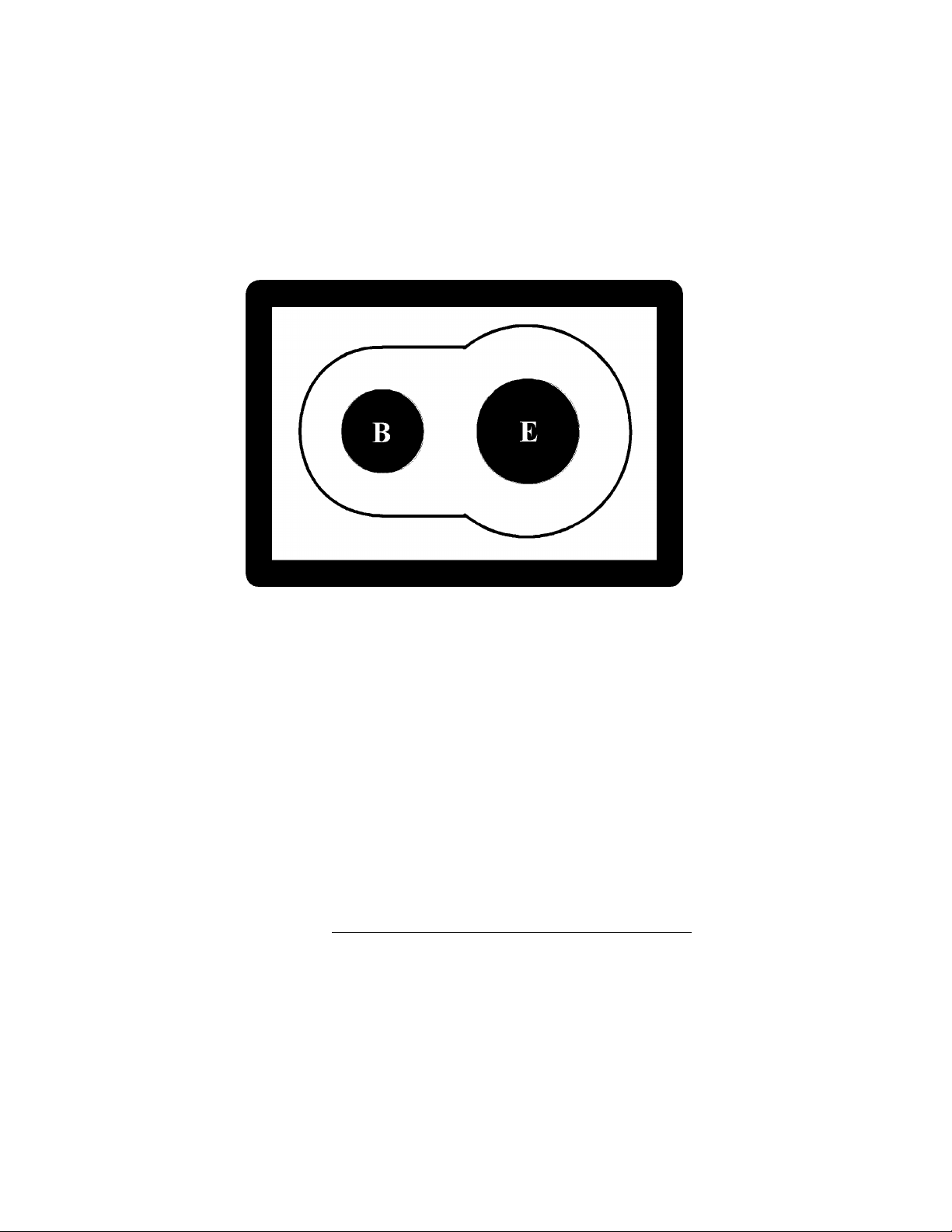
1. Die size...............................................0.015 x 0.019 inches ± 0.001 inch
2. Die thickness.......................................0.010 ± 0.0015 inches
3. Top metal............................................Aluminum 15,000Å minimum, 18,000Å nominal
4. Back metal ..........................................A. Gold 2,500Å minimum, 3,000Å nominal
B. Eutectic Mount – No Gold
5. Backside.............................................Collector
6. Bonding pad........................................ B = 0.003 inches, E = 0.004 inches diameter
7. Passivation.........................................Si3N4 (Silicon Nitride) 2kÅ min, 2.2kÅ nom.
FIGURE 4. Physical dimensions, JANHC and JANKC die, A - version.
5
Page 6
MIL-PRF-19500/376E
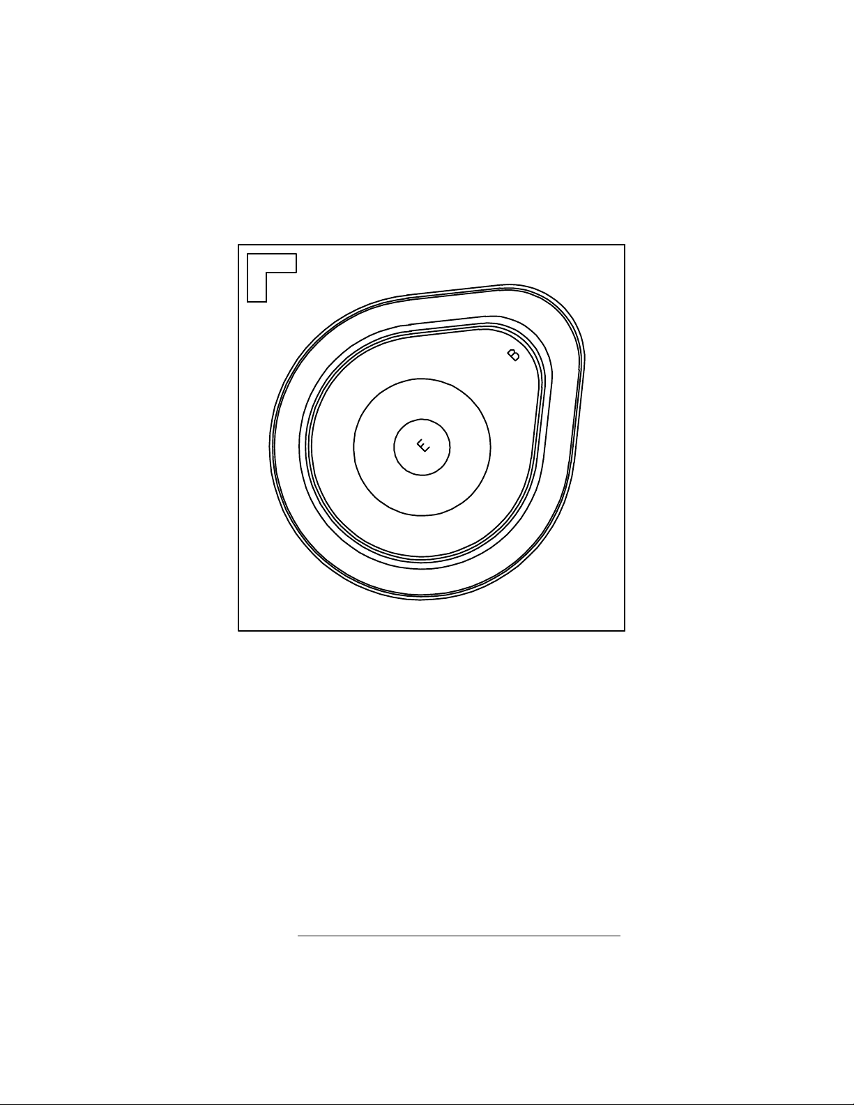
B - version
Die size:.....................................................0.018 x 0.018 inches
Die thickness: ............................................ 0.008 ± 0.0016 inches
Base pad: .................................................. 0.0025 inches diameter
Emitter pad:............................................... 0.003 inches diameter
Back metal:................................................ Gold, 6500 ± 1950 Å
Top metal: ................................................. Aluminum, 19500 ± 2500 Å
Back side:..................................................Collector
Glassivation:..............................................SiO2, 7500 ± 1500 Å
FIGURE 5. Physical dimensions, JANHC and JANKC die, B - version.
6
Page 7

1.4 Primary electrical characteristics.
MIL-PRF-19500/376E
NF
h
FE2
h
FE5
IC = 10 µA dc, VCE = 5 V dc
Rg = 10 kΩ
Min
Max
f = 100 Hz f = 1000 Hz f = 10 kHz VCE = 5 V dc
IC = 10 µA dc
dB
dB
dB
200
7.5
3
2
500
VCE = 5 V dc
IC = 1 mA dc
250
800
2. APPLICABLE DOCUMENTS
2.1 General. The documents listed in this section are specified in sections 3 and 4 of this specification. This
section does not include documents cited in other sections of this specification or recommended for additional
information or as examples. While every effort has been made to ensure the completeness of this list, document
users are cautioned that they must meet all specified requirements documents cited in sections 3 and 4 of this
specification, whether or not they are listed.
2.2 Government documents.
2.2.1 Specifications, standards, and handbooks. The following specifications, standards, and handbooks form a
part of this document to the extent specified herein. Unless otherwise specified, the issues of these documents are
those listed in the issue of the Department of Defense Index of Specifications and Standards (DoDISS) and
supplement thereto, cited in the solicitation (see 6.2).
SPECIFICATION
DEPARTMENT OF DEFENSE
MIL-PRF-19500 - Semiconductor Devices, General Specification for.
STANDARD
DEPARTMENT OF DEFENSE
MIL-STD-750 - Test Methods for Semiconductor Devices.
(Unless otherwise indicated, copies of the above specifications, standards, and handbooks are available from the
Document Automation and Production Services (DAPS), Building 4D (DPM-DODSSP), 700 Robbins Avenue,
Philadelphia, PA 19111-5094.)
2.3 Order of precedence. In the event of a conflict between the text of this document and the references cited
herein, the text of this document takes precedence. Nothing in this document, however, supersedes applicable laws
and regulations unless a specific exemption has been obtained.
7
Page 8

MIL-PRF-19500/376E
3. REQUIREMENTS
3.1 General. The requirements for acquiring the product described herein shall consist of this document and
MIL-PRF-19500.
3.2 Qualification. Devices furnished under this specification shall be products that are manufactured by a
manufacturer authorized by the qualifying activity for listing on the applicable qualified manufacturer’s list (QML)
before contract award (see 4.2 and 6.3).
3.3 Abbreviations, symbols, and definitions. Abbreviations, symbols, and definitions used herein shall be as
specified in MIL-PRF-19500.
3.4 Interface and physical dimensions. The interface and physical dimensions shall be as specified in MIL-PRF19500 and figures 1, 2, 3, 4, and 5 herein.
3.4.1 Lead finish. Unless otherwise specified, lead finish shall be solderable in accordance with MIL-PRF-19500,
and herein.
3.5 Marking. Marking shall be in accordance with MIL-PRF-19500. At the option of the manufacturer, marking
may be omitted from the body, but shall be retained on the initial container.
3.6 Electrical performance characteristics. Unless otherwise specified herein, the electrical performance
characteristics are as specified in 1.3, 1.4, and table I.
3.7 Electrical test requirements. The electrical test requirements shall be the subgroups specified in table I
herein.
3.8 Workmanship. Semiconductor devices shall be processed in such a manner as to be uniform in quality and
shall be free from other defects that will affect life, serviceability, or appearance.
4. VERIFICATION
4.1 Classification of inspections. The inspection requirements specified herein are classified as follows:
a. Qualification inspection (see 4.2).
b. Screening (see 4.3).
c. Conformance inspection (see 4.4).
4.2 Qualification inspection. Qualification inspection shall be in accordance with MIL-PRF-19500 and as
specified herein.
4.2.1. JANHC and JANKC Qualification. JANHC and JANKC qualification inspection shall be in accordance with
MIL-PRF-19500.
8
Page 9

MIL-PRF-19500/376E
4.3 Screening (JANS, JANTX, and JANTXV levels only). Screening shall be in accordance with table IV of
MIL-PRF-19500, and as specified herein. The following measurements shall be made in accordance with table I
herein. Devices that exceed the limits of table I herein shall not be acceptable.
Screen (see table
Measurement
IV
of MIL-PRF-
JANS level JANTX and JANTXV levels
19500)
3c Thermal impedance (see 4.3.2) Thermal impedance (see 4.3.2)
9 I
CBO2
, h
FE4
Not applicable
10 48 hours minimum 48 hours minimum
11 I
; h
CBO2
∆I
CBO2
;
FE4
= 100% of initial value or 2 nA dc,
I
CBO2
,h
FE4
whichever is greater.
∆h
= ±15%
FE4
12 See 4.3.1
240 hours minimum
13 Subgroups 2 and 3 of table I herein;
∆I
= 100% of initial value or 2 nA dc,
CBO2
whichever is greater;
∆h
= ±15%
FE4
See 4.3.1
80 hours minimum
Subgroup 2 of table I herein;
∆I
= 100% of initial value or 2 nA
CBO2
dc, whichever is greater;
∆h
= ±25%
FE4
4.3.1 Power burn-in conditions. Power burn-in conditions are as follows: VCB = 10 to 30 V dc:
Power shall be applied to achieve TJ = 135°C minimum and a minimum power dissipation = 75 percent of
maximum rated PT (see 1.3). TA = room ambient as defined in 4.5 of MIL-STD-750.
NOTE: No heat sink or forced air cooling on the devices shall be permitted.
4.3.2 Thermal impedance (Z
measurements). The Z
θJX
measurements shall be performed in accordance
θJX
with method 3131 of MIL-STD-750.
a. IM measurement current -------------5 mA.
b. IH forward heating current -----------50 mA (min).
c. tH heating time -------------------------25 - 30 ms.
d. tmd measurement delay time ------60 µs max.
e. VCE collector-emitter voltage ------10 V dc minimum.
The maximum limit for Z
under these test conditions are Z
θJX
(max) = 150°C/W for 2N2484, Z
θJX
for 2N2484UA and 2N2484UB.
9
(max) = 67°C/W
θJX
Page 10

MIL-PRF-19500/376E
4.4 Conformance inspection. Conformance inspection shall be in accordance with MIL-PRF-19500, and as
specified herein. If alternate screening is being performed in accordance with MIL-PRF-19500, a sample of
screened devices shall be submitted to and pass the requirements of group A1 and A2 inspection only (table VIb,
group B, subgroup 1 is not required to be performed again if group B has already been satisfied in accordance with
4.4.2).
4.4.1 Group A inspection. Group A inspection shall be conducted in accordance with MIL-PRF-19500 and table I
herein.
4.4.2 Group B inspection. Group B inspection shall be conducted in accordance with the conditions specified for
subgroup testing in table VIa (JANS) of MIL-PRF-19500 and 4.4.2.1. Electrical measurements (end-points) shall be
in accordance with group A, subgroup 2 herein. Delta requirements shall be in accordance with table III herein.
See 4.4.2.2 for JAN, JANTX, and JANTXV group B testing. Electrical measurements (end-points) and delta
requirements for JAN, JANTX, and JANTXV shall be after each step in 4.4.2.2 and shall be in accordance with
group A, subgroup 2 herein. Delta requirements shall be after each step and shall be in accordance with table III
herein.
4.4.2.1 Group B inspection, table VIa (JANS) of MIL-PRF-19500.
Subgroup Method Condition
B4 1037 VCB = 10 V dc
B5 1027 VCB = 10 V dc; TA = +125°C ±25°C for 96 hours with PT adjusted according to the chosen
TA to give TJ = +275°C minimum. Optionally, the test may be conducted for
minimum 216 hours with PT adjusted to achieve TJ = 225°C minimum, sample size (for
option) n = 45, c = 0. In this case, the ambient temperature shall be adjusted such that a
minimum 75 percent of maximum rated PT (see 1.3) is applied to the device under test.
(Note: If a failure occurs, resubmission shall be at the test conditions of the original
sample.)
4.4.2.2 Group B inspection, (JAN, JANTX, and JANTXV). Separate samples may be used for each step. In the
event of a group B failure, the manufacturer may pull a new sample at double size from either the failed assembly
lot or from another assembly lot from the same wafer lot. If the new “assembly lot” option is exercised, the failed
assembly lot shall be scrapped.
Step Method Condition
1 1039 Steady-state life: Test condition B, 340 hours, VCB = 10 -30 V dc, TJ = 150°C min.,
external heating of the device under test to achieve TJ = +150°C minimum is allowed
provided that a minimum of 75% of rated power is dissipated. No heat sink or forced-air
cooling on the devices shall be permitted. n = 45 devices, c = 0
2 1039 The steady state life test of step 1 shall be extended to 1,000 hours for each die design.
Samples shall be selected from a wafer lot every twelve months of wafer production.
Group B, step 2 shall not be required more than once for any single wafer lot. n = 45,
c = 0.
3 1032 High-temperature life (non-operating), t = 340 hours, TA = +200°C. n = 22, c = 0.
10
Page 11

MIL-PRF-19500/376E
4.4.2.3 Group B sample selection. Samples selected from group B inspection shall meet all of the following
requirements:
a. For JAN, JANTX, and JANTXV, samples shall be selected randomly from a minimum of three wafers (or
from each wafer in the lot) from each wafer lot. For JANS, samples shall be selected from each inspection
lot. See MIL-PRF-19500.
b. Must be chosen from an inspection lot that has been submitted to and passed group A, subgroup 2
conformance inspection. When the final lead finish is solder or any plating prone to oxidation at high
temperature, the samples for life test (subgroups B4 and B5 for JANS, and group B for JAN, JANTX, and
JANTXV) may be pulled prior to the application of final lead finish.
4.4.3 Group C inspection, Group C inspection shall be conducted in accordance with the conditions specified for
subgroup testing in table VII of MIL-PRF-19500, and in 4.4.3.1 (JANS).and 4.4.3.2 (JAN, JANTX, and JANTXV)
herein for group C testing. Electrical measurements (end-points) shall be in accordance with group A, subgroup 2
herein. Delta requirements shall be in accordance with table III herein.
4.4.3.1 Group C inspection, table VII (JANS) of MIL-PRF-19500.
Subgroup Method Condition
C2 2036 Test condition E (not applicable to UA and UB suffix devices).
C6 1026 1,000 hours at VCB = 10 -30 V dc; power shall be applied to achieve TJ = 150°C minimum
and a minimum power dissipation PD = 75 percent of maximum rated PT as defined in 1.3
herein.
4.4.3.2 Group C inspection, table VII (JAN, JANTX, and JANTXV) of MIL-PRF-19500.
Subgroup Method Condition
C2 2036 Test condition E (not applicable to UA and UB suffix devices).
C6 Not applicable.
4.4.3.3 Group C sample selection. Samples for subgroups in group C shall be chosen at random from any
inspection lot containing the intended package type and lead finish procured to the same specification which is
submitted to and passes group A tests for conformance inspection. Testing of a subgroup using a single device
type enclosed in the intended package type shall be considered as complying with the requirements for that
subgroup.
4.4.4 Group E inspection. Group E inspection shall be performed for qualification or re-qualification only. The
tests specified in table II herein must be performed to maintain qualification.
4.5 Method of inspection. Methods of inspection shall be as specified in the appropriate tables and as follows.
4.5.1 Pulse measurements. Conditions for pulse measurement shall be as specified in section 4 of MIL-STD-
750.
11
Page 12

MIL-PRF-19500/376E
TABLE I. Group A inspection.
MIL-STD-750 Limit
Inspection 1/
Method Conditions
Subgroup 1 2/
Visual and mechanical
2071 n = 45 devices, c = 0
examination 3/
Solderability 3/ 4/ 2026 n = 15 leads, c = 0
Resistance to solvents 3/ 4/ 5/ 1022 n = 15 devices, c = 0
Temperature cycling 3/ 4/ 1051 Test condition C, 25 cycles.
n = 22 devices, c = 0
Hermetic seal 4/ 1071 n = 22 devices, c = 0
Fine leak
Gross leak
Electrical measurements 4/ Group A, subgroup 2
Bond strength 3/ 4/ 2037
Precondition TA = +250°C at
t = 24 hrs or TA = 300°C at
t = 2 hrs; n = 11 wires, c = 0
Subgroup 2
Collector to emitter breakdown
voltage
3011 Bias condition D; IC = 10 mA dc
pulsed (see 4.5.1)
Collector to base cutoff current 3036 Bias condition D; VCB = 60 V dc I
Symbol
V
(BR)CEO
CBO1
Min Max Unit
60 V dc
10
µA dc
Emitter to base cutoff current 3061 Bias condition D; VEB = 6 V dc I
Collector to base cutoff current 3036 Bias condition D; VCB = 45 V dc I
Collector to emitter cutoff
3041 Bias condition D; VCE = 5 V dc I
current
Emitter to base cutoff current 3061 Bias condition D; VEB = 5 V dc I
Collector to emitter cutoff
3041 Bias condition C; VCE = 45 V dc I
current
Forward-current transfer ratio 3076
VCE = 5 V dc; IC = 1 µA dc
See footnote at end of table.
12
EBO1
CBO2
CEO
EBO2
CES
h
FE1
45
10
µA dc
5 nA dc
2 nA dc
2 nA dc
5 nA dc
Page 13

MIL-PRF-19500/376E
TABLE I. Group A inspection - Continued.
MIL-STD-750 Limit
Symbol
Inspection 1/
Method Conditions
Subgroup 2 - continued.
Forward-current transfer ratio 3076
Forward-current transfer ratio 3076
Forward-current transfer ratio 3076
VCE = 5 V dc; IC = 10 µA dc
VCE = 5 V dc; IC = 100 µA dc
VCE = 5 V dc; IC = 500 µA dc
Forward-current transfer ratio 3076 VCE = 5 V dc; IC = 1 mA dc h
Forward-current transfer ratio 3076 VCE = 5 V dc; IC = 10 mA dc
pulsed (see 4.5.1)
Collector to emitter voltage
3071
IC = 1.0 mA dc; IB = 100 µA dc
V
(saturated)
Base emitter voltage
(nonsaturated)
3066 Test condition B; VCE = 5 V dc;
IC = 100 µA dc
V
Subgroup 3
High-temperature operation
TA = +150°C
Collector to base cutoff current 3036 Bias condition D; VCB = 45 V dc I
Low-temperature operation
TA = -55°C
h
FE2
h
FE3
h
FE4
FE5
h
FE6
CE(sat)
BE(ON)
CBO3
Min Max Unit
200 500
225 675
250 800
250 800
225 800
0.3 V dc
0.5 0.7 V dc
10
µA dc
Forward-current transfer ratio 3076
Subgroup 4
Magnitude of common emitter
small-signal short-circuit
forward-current transfer ratio
Magnitude of common emitter
small-signal short-circuit
forward- current transfer ratio
Small-signal open-circuit
output admittance
Small-signal open- circuit
reverse-voltage transfer ratio
Small-signal short- circuit input
impedance
See footnote at end of table.
VCE = 5 V dc; IC = 10 µA dc
3306
VCE = 5 V dc; IC = 50 µA dc;
f = 5 MHz
3306
VCE = 5 V dc; IC = 500 µA dc;
f = 30 MHz
3216 VCE = 5 V dc; IC = 1.0 mA dc;
f = 1 kHz
3211 VCE = 5 V dc; IC = 1.0 mA dc;
f = 1 kHz
3201 VCE = 5 V dc; IC = 1 mA dc;
f = 1 kHz
13
h
FE7
35
|hfe|1 3.0
|hfe|2 2.0 7.0
h
oe
h
re
40
8.0 x
10
h
ie
3.5 24
µmhos
-4
kΩ
Page 14

MIL-PRF-19500/376E
TABLE I. Group A inspection - Continued.
MIL-STD-750 Limit
Inspection 1/
Subgroup 4 - continued.
Small-signal short- circuit
forward current transfer ratio
Open circuit output
capacitance
Input capacitance (output
open-circuited)
Noise figure 3246 f = 100 Hz; VCE = 5 V dc; IC = 10
Noise figure 3246 f = 1 kHz; VCE = 5 V dc; IC = 10
Noise figure 3246 f = 10 kHz; VCE = 5 V dc; IC = 10
Noise figure (wideband) 3246 Noise bandwidth = 10 Hz to 15.7
Subgroups 5 and 6
Not applicable
Method Conditions
3206 VCE = 5 V dc; IC = 1 mA dc;
f = 1 kHz
3236 VCB = 5 V dc; IE = 0;
100 kHz ≤ f ≤ 1 MHz
3240 VEB = 0.5 V dc; IC = 0;
100 kHz ≤ f ≤ 1 MHz
µA dc; Rg = 10 kΩ;
µA dc; Rg = 10 kΩ;
µA dc; Rg = 10 kΩ;
kHz; VCE = 5 V dc; IC = 10 µA dc;
Rg = 10 kΩ;
Symbol
Min Max Unit
h
fe
C
obo
C
ibo
NF1 7.5 dB
NF2 3 dB
NF3 2 dB
NF4 3 dB
250 900
5.0 pF
6.0 pF
Subgroup 7 4/
Decap internal visual (design
verification)
2075 n = 1 device, c = 0
1/ For sampling plan see MIL-PRF-19500.
2/ For resubmission of failed subgroup A1, double the sample size of the failed test or sequence of tests. A
failure in group A, subgroup 1 shall not require retest of the entire subgroup. Only the failed test shall be rerun
upon submission.
3/ Separate samples may be used.
4/ Not required for JANS devices.
5/ Not required for laser marked devices.
14
Page 15

MIL-PRF-19500/376E
TABLE II. Group E inspection (all quality levels) - For qualification only.
Inspection MIL-STD-750 Qualification
Method Conditions
Subgroup 1
Temperature cycling
(air to air)
Hermetic seal
Fine leak
Gross leak
Electrical measurements
Subgroup 2
Intermittent life
Electrical measurements
Subgroup 3
Not applicable
Subgroup 4
Not applicable
1051
1071
1037
12 devices
c = 0
Test condition C, 500 cycles
See group A, subgroup 2 and table III herein.
45 devices
c = 0
Intermittent operation life: VCB = 10 V dc ,
6,000 cycles.
See group A, subgroup 2 and table III herein.
Subgroup 5
Not applicable
15
Page 16

MIL-PRF-19500/376E
TABLE III. Groups B and C delta measurements. 1/ 2/ 3/
Step Inspection MIL-STD-750 Symbol Limit Unit
Method Conditions
4/
1 Forward-current transfer
ratio
3076 VCE = 5 V dc; IC = 500
µA dc; pulsed see 4.5.1
∆h
FE4
±25 percent change from
initial recorded reading
2. Collector to emitter
voltage (saturated)
3. Collector to emitter
cutoff current
3071 IC = 1.0 mA dc; IB = 100
µA dc
3041 Bias condition C;
VCB = 45 V dc
∆V
4/ 5/
∆I
CES
4/
CE(sat)
±50 mV dc change from
previously measured value.
100 percent of initial value
or 2 nA dc, whichever is
greater.
1/ The delta measurements for group B, table VIa (JANS) of MIL-PRF-19500 are as follows:
a. Subgroup 4, see table III herein, step 2.
b. Subgroup 5, see table III herein, steps 1 and 3.
2/ The delta measurements for 4.4.2.2 herein (group B, JAN, JANTX, and JANTXV) are as follows: Steps 2
and 3 of table III shall be performed after each step in 4.4.2.2 herein.
3/ The delta measurements for group C, table VII of MIL-PRF-19500 are as follows: Subgroup 6, see table III
herein, steps 1 and 3 for JANS, step 1 for JAN, JANTX, and JANTXV.
4/ Devices which exceed the group A limits for this test shall not be accepted.
5/ Applies to JANS level only.
16
Page 17

MIL-PRF-19500/376E
5. PACKAGING
5.1 Packaging. For acquisition purposes, the packaging requirements shall be as specified in the contract or
order (see 6.2). When actual packaging of materiel is to be performed by DoD personnel, these personnel need to
contact the responsible packaging activity to ascertain requisite packaging requirements. Packaging requirements
are maintained by the Inventory Control Points' packaging activity within the Military Department or Defense
Agency, or within the Military Departments' System Command. Packaging data retrieval is available from the
managing Military Departments' or Defense Agency's automated packaging files, CD-ROM products, or by
contacting the responsible packaging activity.
6. NOTES
(This section contains information of a general or explanatory nature that may be helpful, but is not mandatory.)
6.1 Intended use. The notes specified in MIL-PRF-19500 are applicable to this specification.
6.2 Acquisition requirements. Acquisition documents should specify the following:
a. Title, number, and date of this specification.
b. Issue of DoDISS to be cited in the solicitation, and if required, the specific issue of individual documents
referenced (see 2.2.1).
c. Lead formation and finish may be specified (see 3.4.1).
d. Type designation and product assurance level.
e. Packaging requirements (see 5.1).
6.3 Qualification. With respect to products requiring qualification, awards will be made only for products which
are, at the time of award of contract, qualified for inclusion in Qualified Manufacturers List QML-19500 whether or
not such products have actually been so listed by that date. The attention of the contractors is called to these
requirements, and manufacturers are urged to arrange to have the products that they propose to offer to the Federal
Government tested for qualification in order that they may be eligible to be awarded contracts or orders for the
products covered by this specification. Information pertaining to qualification of products may be obtained from
Defense Supply Center, Columbus, ATTN: DSCC-VQE, P.O. Box 3990, Columbus, OH 43216-5000.
6.4 Suppliers of JANHC die. The qualified JANHC suppliers with the applicable letter version (example
JANHCA1N645-1) will be identified on the QML.
JANC ordering information
PIN Manufacturer
43611 34156
2N2484 JANHCA2N2484 JANHCB2N2484
JANKCA2N2484 JANKCB2N2484
6.5 Changes from previous issue. Marginal notations are not used in this revision to identify changes with
respect to the previous issue due to the extensiveness of the changes.
17
Page 18

MIL-PRF-19500/376E
Custodians: Preparing activity:
Army - CR DLA - CC
Navy - EC
Air Force - 11 (Project 5961-2309)
NASA - NA
DLA - CC
Review activities:
Army - AR, MI, SM
Navy - AS, CG, MC, SH
Air Force - 13, 19
18
Page 19

STANDARDIZATION DOCUMENT IMPROVEMENT PROPOSAL
1. The preparing activity must complete blocks 1, 2, 3, and 8. In block 1, both the document number and revision
letter should be given.
2. The submitter of this form must complete blocks 4, 5, 6, and 7.
3. The preparing activity must provide a reply within 30 days from receipt of the form.
NOTE: This form may not be used to request copies of documents, nor to request waivers, or clarification of requirements on
current contracts. Comments submitted on this form do not constitute or imply authorization to waive any portion of the
referenced document(s) or to amend contractual requirements.
I RECOMMEND A CHANGE:
1. DOCUMENT NUMBER
MIL-PRF-19500/376E
2. DOCUMENT DATE
31 August 2000
3. DOCUMENT TITLE
SEMICONDUCTOR DEVICE, TRANSISTOR, NPN, SILICON, LOW-POWER TYPES 2N2484, 2N2484UA, 2N2484UB, JAN,
JANTX, JANTXV, JANS, JANHC, AND JANKC
4. NATURE OF CHANGE (Identify paragraph number and include proposed rewrite, if possible. Attach extra sheets as needed.)
5. REASON FOR RECOMMENDATION
6. SUBMITTER
a. NAME (Last, First, Middle initial) b. ORGANIZATION
c. ADDRESS (Include Zip Code) d. TELEPHONE (Include Area Code)
7. DATE SUBMITTED
COMMERCIAL
DSN
FAX
EMAIL
8. PREPARING ACTIVITY
b. TELEPHONE
a. Point of Contact
Alan Barone
c. ADDRESS
Defense Supply Center, Columbus
ATTN: DSCC-VAC
P.O. Box 3990
Columbus, OH 43216-5000
Commercial DSN FAX EMAIL
614-692-0510 850-0510 614-692-6939 alan_barone@dscc.dla.mil
IF YOU DO NOT RECEIVE A REPLY WITHIN 45 DAYS, CONTACT:
Defense Standardization Program Office (DLSC-LM)
8725 John J. Kingman, Suite 2533
Fort Belvoir, VA 22060-6221
Telephone (703) 767-6888 DSN 427-6888
DD Form 1426, Feb 1999 (EG) Previous editions are obsolete WHS/DIOR, Feb 99
 Loading...