

Page 1
120101
查询2N2323A供应商
TECHNICAL DATA
SILICON CONTROLLED RECTIFIER
Qualified per MIL-PRF-19500/276
Devices Qualified
Level
2N2323
2N2323S
2N2323A
2N2323AS
MAXIMUM RATINGS
Reverse Voltage VRM 50 100 200 300 400 Vdc
Working Peak Reverse Voltage VRM 75 150 300 400 500 Vpk
Forward Blocking Voltage V
Average Forward Current
Forward Current Surge Peak
Cathode-Gate Current V
Operating Temperature Top -65 to +125
Storage Junction Temp T
1) This average forward current is for an ambient temperature of 800C and 180 electrical degrees of
conduction.
2) Surge current is non-recurrent. The rate of rise of peak surge current shall not exceed 40 A during
the first 5 µs after switching from the ‘off’ (blocking) to the ‘on’ (conducting) state. This is measured
from the point where the thyristor voltage has decayed to 90% of its initial blocking value.
3) Gate connected to cathode through 1,000 ohm resistor.
4) Gate connected to cathode through 2,000 ohm resistor.
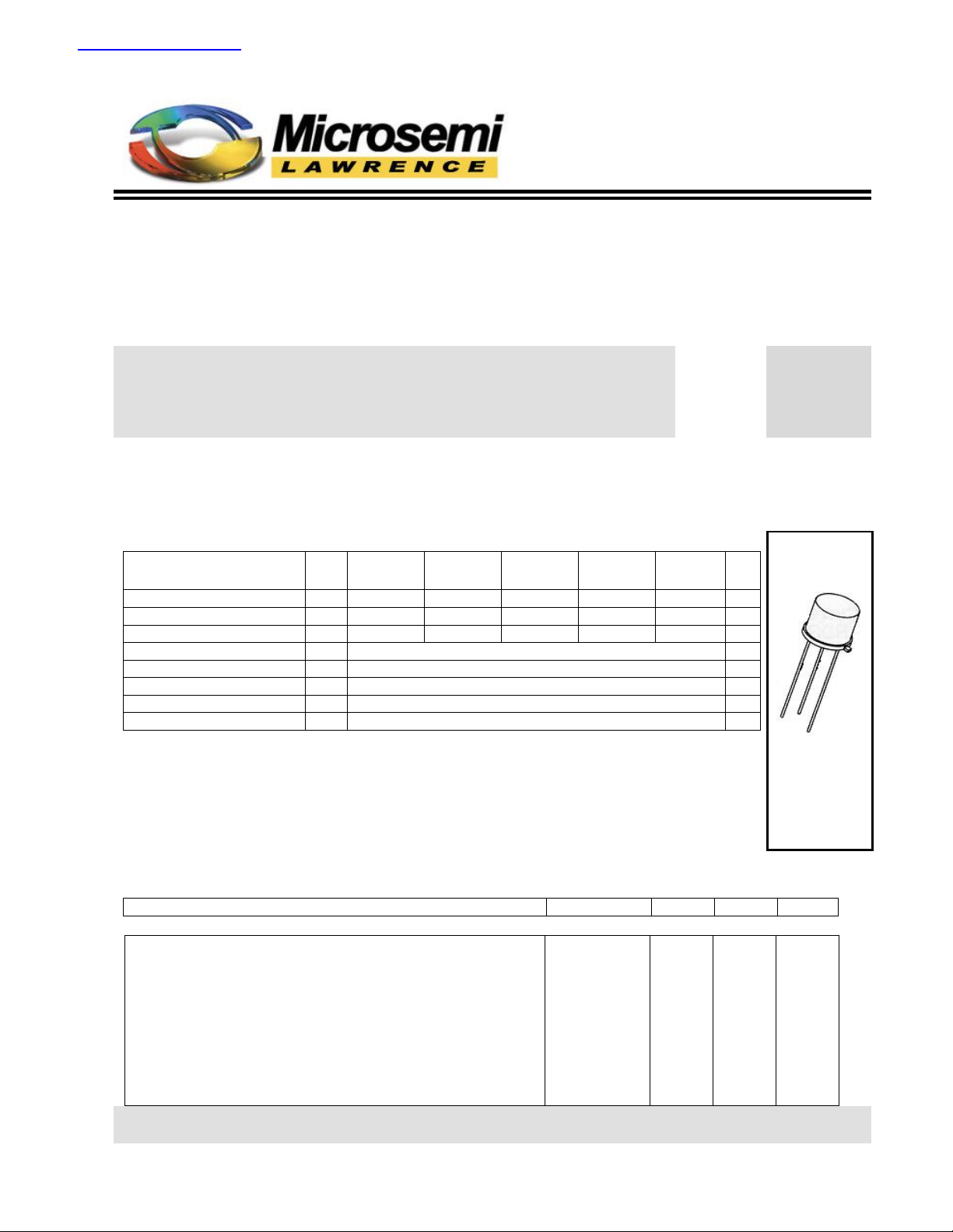
*See appendix A
for package outline
ELECTRICAL CHARACTERISTICS
SUBGROUP 2 TESTING
Reverse Blocking Current
R2 = 1 kµ 2N2323 thru 2N2329
2N2323S thru 2N2329S
R2 = 2 kµ 2N2323A thru 2N2328A
2N2323AS thru 2N2328AS
VR = 50 Vdc 2N2323, S, A, AS
VR = 100 Vdc 2N2324, S, A, AS
VR = 200 Vdc 2N2326, S, A, AS
VR = 300 Vdc 2N2328, S, A, AS
VR = 400 Vdc 2N2329, S,
6 Lake Street, Lawrence, MA 01841
1-800-446-1158 / (978) 794-1666 / Fax: (978) 689-0803
2N2324
2N2324S
2N2324A
2N2324AS
Ratings Sym
FBXM
(1)
IO 0.22 Adc
(2)
I
FSM
KGM
stg
Characteristics Symbol Min. Max. Unit
2N2326
2N2326S
2N2326A
2N2326AS
2N2323,S/
2N2323A,S
(3/4)
50
15 Adc
-65 to +150
2N2328
2N2328S
2N2328A
2N2328AS
2N2324,S/
2N2324A,S
(3/4)
100
2N2329
2N2329S
2N2326,S/
2N2326A,S
200
6 Vpk
2N2328,S/
2N2328A,S
(3/4)
300
0C
0C
I
RBX1
(3/4)
2N2329,S Unit
400
(3)
Vpk
10
JAN
JANTX
JANTXV
TO-5
µAdc
Page 1 of 2
Page 2
120101
2N2323, A, AS, S; 2N2324, A, AS, S; 2N2326, A, AS, S; 2N2328, A, AS, S; 2N232, S JAN SERIES
ELECTRICAL CHARACTERISTICS (con’t)
Forward Blocking Current
R2 = 1 kΩ 2N2323 thru 2N2329
2N2323S thru 2N2329S
R2 = 2 kΩ 2N2323A thru 2N2328A
2N2323AS thru 2N2328AS
VR = 50 Vdc 2N2323, S, A, AS
VR = 100 Vdc 2N2324, S, A, AS
VR = 200 Vdc 2N2326, S, A, AS
VR = 300 Vdc 2N2328, S, A, AS
VR = 400 Vdc 2N2329, S
Reverse Gate Current
VKG = 6 Vdc
Gate Trigger Voltage and Current
V2 = V
Re = 1 kΩ 2N2323 thru 2N2329 and
2N2323S thru 2N2329S
Re = 2 kΩ 2N2323A thru 2N2328A and
2N2323AS thru 2N2328AS
= 6 Vdc; RL = 100 Ω
FBX
Characteristics Symbol Min. Max. Unit
I
FBX1
IKG
V
I
GT1
V
I
GT1
GT1
GT1
0.35
0.35
SUBGROUP 4 TESTING
Exponential Rate of Voltage Rise TA = 1250C
50 Ω ≤ RL ≤ 400 Ω, C = 0.1 to 1.0 µF, repetition rate = 60 pps,
test duration = 15 seconds
dv/dt = 1.8 v/µs, R3 = 1 kΩ 2N2323 thru 2N2329 and
2N2323S thru 2N2329S
dv/dt = 0.7 v/µs, R3 = 2 kΩ 2N2323A thru 2N2328A and
2N2323AS thru 2N2328AS
VAA = 50 Vdc 2N2323, S, A, AS
VAA = 100 Vdc 2N2324, S, A, AS
VAA = 200 Vdc 2N2326, S, A, AS
VAA = 300 Vdc 2N2328, S, A, AS
VAA = 400 Vdc 2N2329, S
Forward “on” Voltage
iFM = 4a (pk) (pulse), pulse width = 8.5 ms, max; duty cycle = 2% max
Holding Current
VAA = 24 Vdc max, IF1 = 100 mAdc, IF2 = 10 mAdc
Gate trigger source voltage = 6 Vdc,
trigger pulse width = 25 µs min., R2 = 330 Ω
R3 = 1 kΩ 2N2323 thru 2N2329 and
2N2323S thru 2N2329S
R3 = 2 kΩ 2N2323A thru 2N2328A and
2N2323AS thru 2N2328AS
V
FBX
VFM
I
HOX
47
95
190
285
380
2.0 mAdc
10
200
0.80
200
0.60
20
µAdc
µAdc
Vdc
µAdc
Vdc
µAdc
Vdc
2.2 V(pk)
6 Lake Street, Lawrence, MA 01841
1-800-446-1158 / (978) 794-1666 / Fax: (978) 689-0803
Page 2 of 2
Page 3

Copyright © Each Manufacturing Company.
All Datasheets cannot be modified without permission.
This datasheet has been download from :
www.AllDataSheet.com
100% Free DataSheet Search Site.
Free Download.
No Register.
Fast Search System.
www.AllDataSheet.com
 Loading...