

Page 1
© 1999 Fairchild Semiconductor Corporation DS009606 www.fairchildsemi.com
April 1988
Revised August 1999
29F52•29F53 8-Bit Registered Transceiver
29F52•29F53
8-Bit Registered Transceiver
General Description
The 29F52 and 29F53 are 8-bit registered transceivers.
Two 8-bit back to back registers store data flowing i n both
directions between two bidirectional buses. Separate clock,
clock enable and 3-STATE output enable signals are provided for each reg ister. The A
0–A7
output pins are guara n-
teed to sink 24 mA while the B
0–B7
output pins are
designed for 64 mA.
The 29F53 is an inverting op tion of the 29F5 2. Both tran s-
ceivers are AMD Am2952/2953 functional equivalents.
Features
■ 8-bit registered transceivers
■ Separate clock, clock enable and 3-STATE output
enable provided for each register
■ AMD Am2952/2953 functional equivalents
■ Both inverting and non-inverting options available
■ 24-Pin slimline package
Ordering Code:
Devices also availab le in Tape and Reel. Specify by appending th e s uffix let t er “X” to the ordering code.
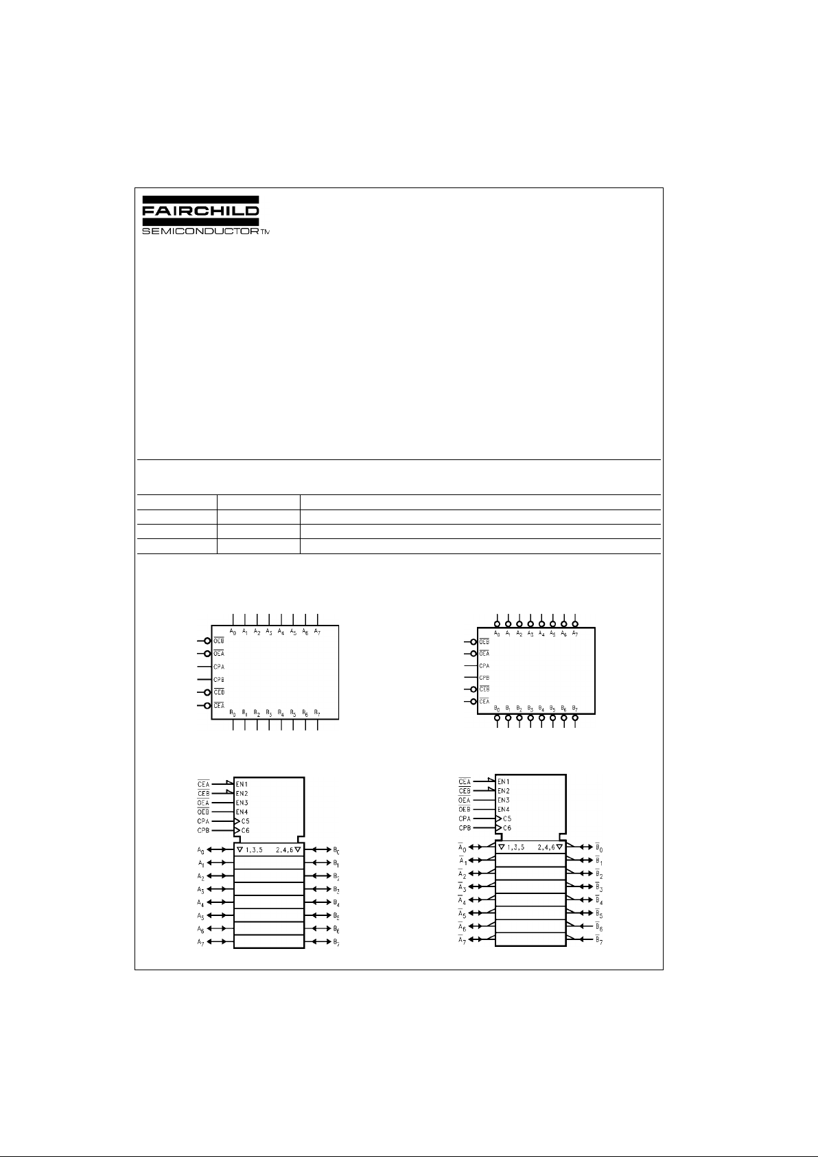
Logic Symbols
29F52
IEEE/IEC
29F52
29F53
IEEE/IEC
29F53
Order Number Package Number Package Description
29F52SC M24B 24-Lead Small Outline Integrated Circuit (SOIC), JEDEC MS-013, 0.300 Wide
29F52SPC N24C 24-Lead Plastic Dual-In-Line Package (PDIP), JEDEC MS-100, 0.300 Wide
29F53SPC N24C 24-Lead Plastic Dual-In-Line Package (PDIP), JEDEC MS-100, 0.300 Wide
Page 2
www.fairchildsemi.com 2
29F52•29F53
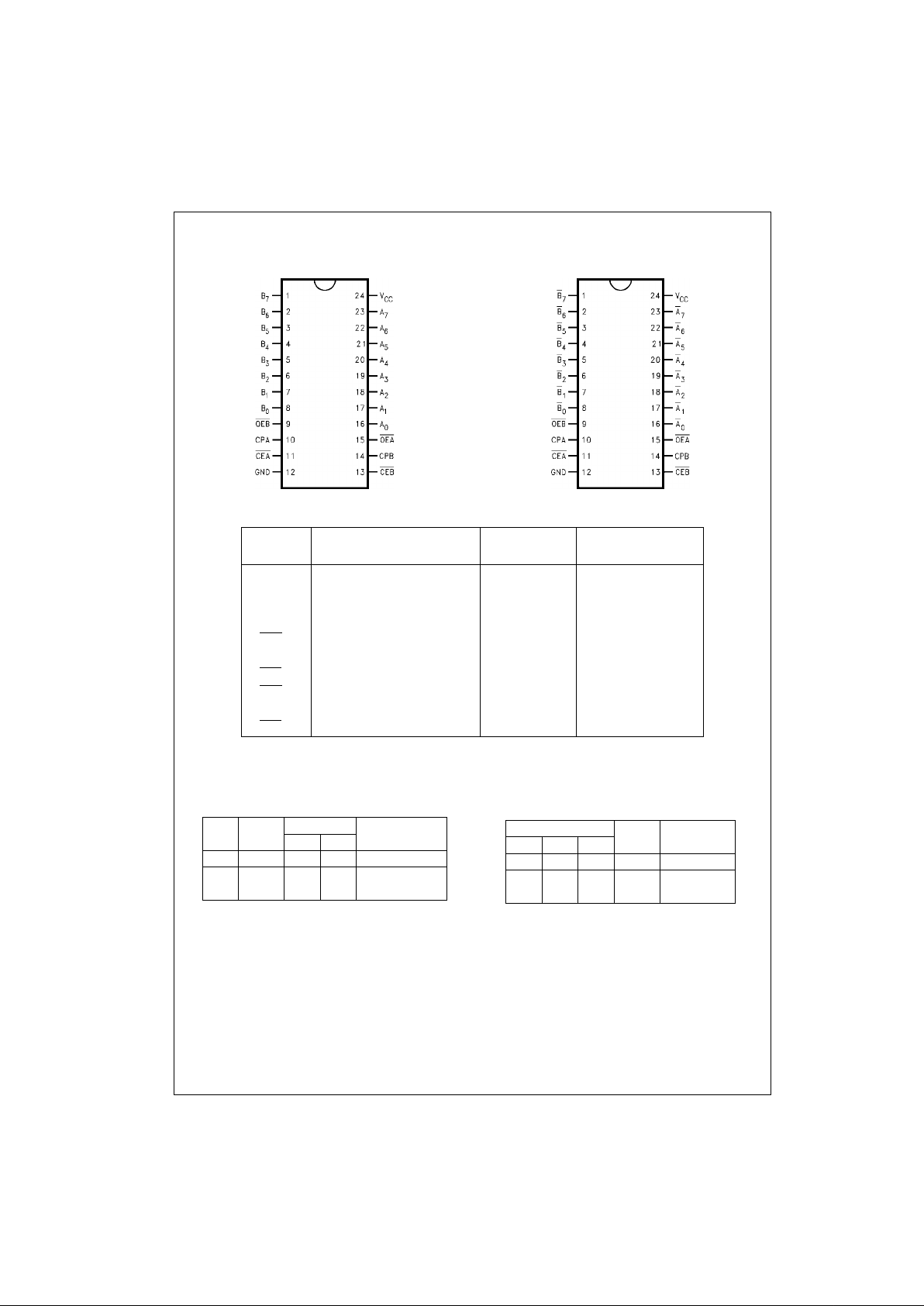
Connection Diagrams
Pin Assignment for DIP and SOIC
29F52
Pin Assignment for DIP
29F53
Unit Loading/Fan Out
Output Control
H = HIGH Voltage Level
L = LOW Voltage Level
X = Immaterial
Z = HIGH Impedance
N = LOW-to-HIGH Transition
NC = No Change
Register Function Table
(Applies to A or B Register)
Pin Names Description
U.L.
Input I
IH/IIL
HIGH/LOW
Output I
OH/IOL
A0–A
7
A-Register Inputs/ 3.5/1.083 70 µA/0.65 mA
B-Register 3-STATE Outputs 150/40 (33.3) −3 mA/24 mA (20 mA)
B
0–B7
B Register Inputs/ 3.5/1.083 70 µA/0.65 mA
A-Register 3-STATE Outputs 600/106.6 (80) −12 mA/64 mA (48 mA)
OEA
Output Enable A-Register 1.0/1.0 20 µA/−0.6 mA
CPA A-Register Clock 1.0/1.0 20 µA/−0.6 mA
CEA
A-Register Clock Enable 1.0/1.0 20 µA/−0.6 mA
OEB
Output Enable B-Register 1.0/1.0 20 µA/−0.6 mA
CPB B-Register Clock 1.0/1.0 20 µA/−0.6 mA
CEB
B-Register Clock Enable 1.0/1.0 20 µA/−0.6 mA
OE
Internal Y-Output
Function
Q 29F52 29F53
H X Z Z Disable Outputs
LLLH
Enable Outputs
LHHL
Inputs Internal
Function
DCPCE Q
X X H NC Hold Data
LNL L
Load Data
HNL H
Page 3
3 www.fairchildsemi.com
29F52•29F53
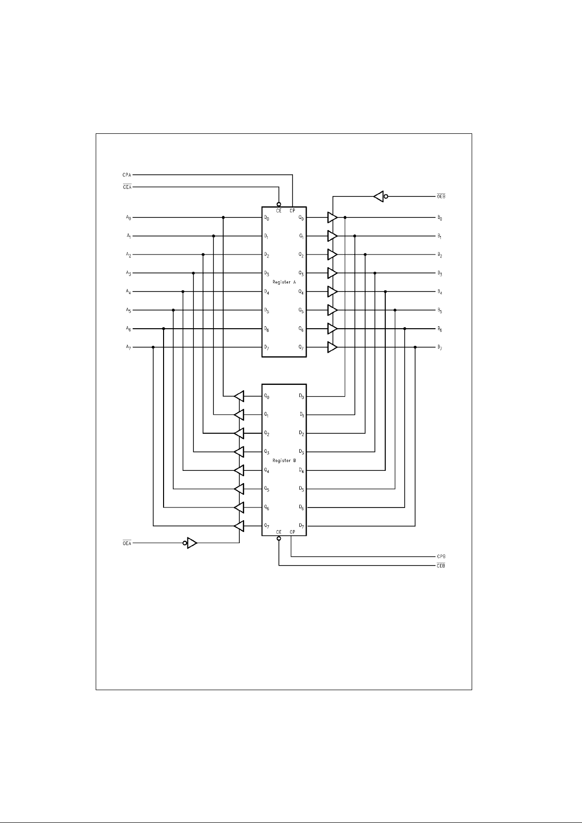
Block Diagrams
29F52
Page 4

www.fairchildsemi.com 4
29F52•29F53
Block Diagrams (continued)
29F53
Page 5

5 www.fairchildsemi.com
29F52•29F53
Absolute Maximum Ratings(Note 1) Recommended Operating
Conditions
Note 1: Absolute maximum ratings are values beyon d which the device
may be damaged or have its useful life impaired . Functional operation
under these condit ions is not implied.
Note 2: Either voltage limit or curren t limit is sufficient to protect in puts.
DC Electrical Characteristics
Storage Temperature −65°C to +150°C
Ambient Temperature under Bias −55°C to +125°C
Junction Temperature under Bias −55°C to +150°C
V
CC
Pin Potential to Ground Pin −0.5V to +7.0V
Input Voltage (Note 2) −0.5V to +7.0V
Input Current (Note 2) −30 mA to +5.0 mA
Voltage Applied to Output
in HIGH State (with V
CC
= 0V)
Standard Output −0.5V to V
CC
3-STATE Output −0.5V to +5.5V
Current Applied to Output
in LOW State (Max) twice the rated I
OL
(mA)
Free Air Ambi ent Temperat ure 0°C to +70°C
Supply Voltage +4.5V to +5.5V
Symbol Parameter Min Typ Max Units
V
CC
Conditions
V
IH
Input HIGH Voltage 2.0 V Recognized as a HIGH Signal
V
IL
Input LOW Voltage 0.8 V Recognized as a LOW Signal
V
CD
Input Clamp Diode Voltage −1.2 V Min IIN = −18 mA (Non I/O Pins)
V
OH
Output HIGH 10% V
CC
2.5
VMin
IOH = −1 mA (An)
Voltage 10% V
CC
2.4 IOH = −3 mA (An, Bn)
10% V
CC
2.0 IOH = −15 mA (Bn)
5% V
CC
2.7 IOH = −1 mA (An)
5% V
CC
2.7 IOH = −3 mA (An, Bn)
V
OL
Output LOW 10% V
CC
0.5
VMin
IOL = 24 mA (An)
Voltage 10% V
CC
0.55 IOL = 64 mA (Bn)
I
IH
Input HIGH Current 20 µAMaxVIN = 2.7V (Non-I/O Pins)
I
BVI
Input HIGH Current
100 µAMaxVIN = 7.0V (Non-I/O Pins)
Breakdown Test
I
BVIT
Input HIGH Current
1.0 mA Max VIN = 5.5V (An, Bn)
Breakdown Test (I/O)
I
IL
Input LOW Current −0.6 mA Max VIN = 0.5V (Non-I/O Pins)
IIH + I
OZH
Output Leakage Current 70 µAMaxV
OUT
= 2.7V (An, Bn)
IIL + I
OZL
Output Leakage Current −650 µAMaxV
OUT
= 0.5V (An, Bn)
I
OS
Output Short-Circuit Current −60 −150 mA Max V
OUT
= 0V (An)
−100 −225 V
OUT
= 0V (Bn)
I
CEX
Output HIGH Leakage Current 250 µAMaxV
OUT
= VCC (An, Bn)
I
ZZ
Bus Drainage Test 500 µA0.0VV
OUT
= 5.25V (An, Bn)
I
CCH
Power Supply Current 130 190 mA Max VO = HIGH
I
CCL
Power Supply Current 190 mA Max VO = LOW
I
CCZ
Power Supply Current 190 mA Max VO = HIGH Z
Page 6

www.fairchildsemi.com 6
29F52•29F53
AC Electrical Characteristics
AC Operating Requirements
Symbol Parameter
TA = +25°CT
A
= −55°C to +125°CTA = 0°C to +70°C
Units
VCC = +5.0V VCC = +5.0V VCC = +5.0V
CL = 50 pF CL = 50 pF CL = 50 pF
Min Typ Max Min Max Min Max
t
PLH
Propagation Delay 3.0 5.5 7.5 2.5 8.5
ns
t
PHL
CPA or CPB to An or B
n
4.0 7.0 9.0 3.5 10.0
t
PZH
Output Enable Time 2.5 5.5 7.5 2.0 8.5
ns
t
PZL
OEA or OEB to An or B
n
3.5 7.0 9.5 3.0 10.5
t
PHZ
Output Disable Time 2.5 6.5 9.0 2.0 10.0
ns
t
PLZ
OEA or OEB to An or B
n
2.5 5.5 7.5 2.0 8.5
Symbol Parameter
TA = +25°CTA = −55°C to +125°CTA = 0°C to +70°C
UnitsVCC = +5.0V VCC = +5.0V VCC = +5.0V
Min Max Min Max Min Max
tS(H) Setup Time, HIGH or LOW 4.0 4.5
ns
tS(L) An or Bn to CPA or CPB 4.0 4.5
tH(H) Hold Time, HIGH or LOW 2.0 2.5
ns
tH(L) An or Bn to CPA or CPB 2.0 2.5
tS(H) Setup Time, HIGH or LOW 1.0 1.5
ns
tS(L)
CEA or CEB to CPA or CPB
4.0 4.5
tH(H) Hold Time, HIGH or LOW 2.0 2.5
ns
tH(L)
CEA or CEB to CPA or CPB
2.0 2.5
tW(H) Pulse Width, HIGH or LOW 3.0 3.5
ns
tW(L) CPA or CPB 3.0 3.5
Page 7

7 www.fairchildsemi.com
29F52•29F53
Physical Dimensions inches (millimeters) unless otherwise noted
24-Lead Small Outline Integrated Circuit (SOIC), JEDEC MS-013, 0.300 Wide
Package Number M24B
Page 8

www.fairchildsemi.com 8
29F52•29F53 8-Bit Registered Transceiver
Physical Dimensions inches (millimeters) unless otherwise noted (Continued)
24-Lead Plastic Dual-In-Line Package (PDIP), JEDEC MS-100, 0.300 Wide
Package Number N24C
Fairchild does not assume any responsibility for use of any circuitry described, no circuit pate nt licenses are implied and
Fairchild reserves the right at any time without notice to change said circuitry and specifications.
LIFE SUPPORT POLICY
FAIRCHILD’S PRODUCTS ARE NOT AUTHORIZED FOR USE AS CRITICAL COMPONENTS IN LIFE SUPPORT
DEVICES OR SYSTEMS WITHOUT THE EXPRESS WRITTEN APPROVAL OF THE PRESIDENT OF FAIRCHILD
SEMICONDUCTOR CORPORATION. As used herein:
1. Life support devices or syste ms are devices or syste ms
which, (a) are intended for surgical implant into the
body, or (b) support or sustain life, and (c) whose failure
to perform when properly used in accordance with
instructions for use provided in the labeling, can be reasonably expected to result in a significant inju ry to the
user.
2. A critical compon ent in any com ponen t of a life su pport
device or system whose failu re to perform can be reasonably expected to ca use the fa i lure of the life su pp ort
device or system, or to affect its safety or effectiveness.
www.fairchildsemi.com
 Loading...