

Page 1

查询S29PL127N70FAI000供应商
S29PL-N MirrorBit™ Flash Family
29PL256N, S29PL127N, S29PL129N,
256/128/128 Mb (16/8/8 M x 16-Bit) CMOS, 3.0 Volt-only
Simultaneous Read/Write, Page-Mode Flash Memory
Data Sheet
Notice to Readers: This document indicates states the current technical
specifications regarding the Spansion product(s ) described herein. The
Preliminary status of this document indicates that a product qualification has
been completed, and that initial production has begun. Due to the phases of
the manufacturing process that require maintaining efficiency and quality , this
document may be revised by subsequent versions or modifications due to
changes in technical specifications.
PRELIMINARY
Publication Number S29PL-N_00 Revision A Amendment 4 Issue Date November 23, 2005
Page 2

Notice On Data Sheet Designations
Spansion LLC issues data sheets with Advance Information or Preliminary designatio ns t o a dvise
readers of product information or intended specif ications throughout the product life cycle, includ
ing development, qualification, initial production, and full production. In all cases, however,
readers are encouraged to verify that they have the latest information before finalizing their de
sign. The following descriptions of Spansion data sheet designations are presented here to
highlight their presence and definitions.
Advance Information
The Advance Information designation indicates that Spansion LLC is developing one or more specific products, but has not committed any design to production. Information presented in a
document with this designation is likely to change, and in some cases, development on the prod
uct may discontinue. Spa nsion LLC therefore places the following conditions upon Advance
Information content:
“This document contains information on one or more products un der development at Spansion LL C. The
information is intended to help you evaluate this product. Do not design in this product without contacting the factory. Spansion LLC reserves the right to change or discontinue work on this proposed
product without notice.”
Preliminary
The Preliminary designation indicates that the product development has progressed such that a
commitment to production has taken place. This designation covers several aspects of the product
life cycle, including product qualification, initial production, and the subsequent phases in the
manufacturing process that occur before full production is achieved. Changes to the technical
specifications presented in a Preliminary document should be expected while keeping these as
pects of production under consideration. Spansion places the following conditions upon
Preliminary content:
“This document states the current technical specifications regarding the Spansion product(s) described
herein. The Preliminary status of this document indicates that product qualification has been completed,
and that initial production has begun. Due to the phases of the manufacturing process that require
maintaining efficiency and quality, this document may be revised by subsequent versions or modifications due to changes in technical specifications.”
Combination
Some data sheets will contain a combination of products with different designations (Advance Information, Preliminary, or Full Production). This type of document will distinguish these products
and their designations wherever necessary, typically on the first page, the ordering information
page, and pages with DC Characteristics table and AC Erase and Program table (in the table
notes). The disclaimer on the first page refers the reader to the notice on this page.
Preliminary
-
-
-
-
Full Production (No Designation on Document)
When a product has been in production for a period of time such that no changes or only nominal
changes are expected, the Preliminary designation is removed from the data sheet. Nominal
changes may include those affecting the number of ordering part numbers available, such as the
addition or deletion of a speed option, temperature range, package type, or V
range. Chang es
IO
may also include those needed to clarify a description or to correct a typographical error or incor
rect specification. Spansion LLC applies the following conditions to documents in this category:
“This document states the current technical specifications regarding the Spansion product(s) described
herein. Spansion LLC deems the products to have been in sufficient production volume such that subsequent versions of this document are not e xpected to chan ge. Howeve r, typographical or specification
corrections, or modifications to the valid combinations offered may occur.”
Questions regarding these document designations may be directed to your local AMD or Fujitsu
sales office.
ii S29PL-N MirrorBit™ Flash Family S29PL-N_00_A4 November 23, 2005
-
Page 3

S29PL-N MirrorBit™ Flash Family
S29PL256N, S29PL127N, S29PL129N,
256/128/128 Mb (16/8/8 M x 16-Bit) CMOS, 3.0 Volt-only
Simultaneous Read/Write, Page-Mode Flash Memory
Data Sheet
PRELIMINARY
General Description
The Spansion S29PL-N is the latest generation 3.0-Volt page mode read family fabricated using the 110 nm Mirrorbit
Flash process technology . These 8-word page-mode Flash devices are capable of performing simultaneous read and write
operations with zero latency on two separate banks. These devices offer fast page access times of 25 to 30 ns, with
corresponding random access times of 65 ns, 70 ns, and 80 ns respectively , allowing high speed microp rocessors to operate without wait states. The S29PL129N device offers the additional feature of dual chip enable inputs (CE1# and
CE2#) that allow each half of the memory space to be controlled separately.
Distinctive Characteristics
Architectural Advantages
32-Word Write Buffer
Dual Chip Enable Inputs (only for S29PL129N)
— Two CE# inputs control selection of each half of the
memory space
Single Power Supply Operation
— Full Voltage r ange of 2.7 – 3.6 V read, erase, and
program operations for ba ttery-powered applications
— Voltage range of 2.7 – 3.1 V valid for PL-N MCP
products
Simultaneous Read/Write Operation
— Data can be continuously read from one bank while
executing erase/program functions in another bank
— Zero latency switching from write to read operations
4-Bank Sector Architecture with Top and Bottom
Boot Blocks
256-Word Secured Silicon Sector Region
— Up to 128 factory-locked words
— Up to 128 customer-lockable words
Manufactured on 0.11 µm Process Technology
Data Retention of 20 years Typical
Cycling Endurance of 100,000 Cycles per Sector
Typical
Hardware Features
WP#/ACC (Write Protect/Acceleration) Input
—At VIL, hardware level protection for the first and last
two 32 Kword sectors.
—At VIH, allows the use of DYB/PPB sector protection
—At VHH, provides accelerated programming in a
factory setting
Dual Boot and No Boot Options
Low V
Write Inhibit
CC
Security Features
Persistent Sector Protection
— A command sector protection method to lock
combinations of individual sectors to prevent
program or erase operations within that sector
— Sectors can be locked and unlocked i n-system at V
level
Password Sector Protection
— A sophisticated sector protection method locks
combinations of individual sectors to p revent program
or erase operations within that sector using a user
defined 64-bit password
TM
CC
Performance Characteristics
Read Access Times (@ 30 pF, Industrial Temp.)
Random Access Time, ns (t
Page Access Time, ns (t
Max CE# Access Time, ns (t
Max OE# Access Time, ns (t
Current Consumption (typ ical values)
8-Word Page Read 6 mA
Simultaneous Read/Write 65 mA
Program/Erase 25 mA
Standby 20 µA
Publication Number S29PL-N_00 Revision A Amendment 4 Issue Date November 23, 2005
)657080
ACC
)253030
PACC
)657080
CE
)253030
OE
Typical Program & Eras e Times (typical values) (See Note)
Typical Word 40 µs
Typical Effective Word (32 words in buffer) 9.4 µs
Accelerated Write Buffer Program 6 µs
Typical Sector Erase Time (32-Kword Sector) 300 ms
Typical Sector Erase Time (128-Kword Sector) 1.6 s
Note: : Typical program and erase times assume the following
conditions: 25°C, 3.0
S29PL-N
256
129
127
V VCC, 10,000 cycles; checkerboard data pattern.
VBH064
8.0 x 11.6 mm,
64-ball
Package Options
VBH084
8.0 x 11.6 mm,
84-ball
11 x 13 mm, 64-ball
LAA064
Fortified BGA
Page 4

Contents
Preliminary
1 Ordering Information. . . . . . . . . . . . . . . . . . . . . . . . . . . . . . . . . . . . . . . . . . . 6
2 Input/Output Descriptions and Logic Symbols . . . . . . . . . . . . . . . . . . . . . . 7
3 Block Diagram . . . . . . . . . . . . . . . . . . . . . . . . . . . . . . . . . . . . . . . . . . . . . . . . 8
4 Connection Diagrams/Physical Dimensions. . . . . . . . . . . . . . . . . . . . . . . . . 9
4.1 Special Handling Instructions for FBGA Package. . . . . . . . . . . . . . . . . . . . . . . . . . . . . . . . . . .9
4.2 VBH084, 8.0 x 11.6 mm . . . . . . . . . . . . . . . . . . . . . . . . . . . . . . . . . . . . . . . . . . . . . . . . . . . . . . .9
4.2.1 Connection Diagram – S29PL256N MCP Compatible Package. . . . . . . . . . . . . . . . . .9
4.2.2 Physical Dimensions – VBH084, 8.0 x 11.6 mm. . . . . . . . . . . . . . . . . . . . . . . . . . . . . . 10
4.3 VBH064, 8 x 11.6 mm. . . . . . . . . . . . . . . . . . . . . . . . . . . . . . . . . . . . . . . . . . . . . . . . . . . . . . . . 11
4.3.1 Connection Diagram – S29PL127N MCP Compatible Package . . . . . . . . . . . . . . . . . 11
4.3.2 Connection Diagram – S29PL129N MCP Compatible Package . . . . . . . . . . . . . . . . . 12
4.3.3 Physical Dimensions – VBH064, 8 x 11.6 mm – S29PL-N . . . . . . . . . . . . . . . . . . . . . . 13
4.3.4 Connection Diagram – S29PL-N Fortified Ball Grid Array Package . . . . . . . . . . . . . 14
4.3.5 Physical Dimensions – LAA064, 11 x 13 mm – S29PL-N . . . . . . . . . . . . . . . . . . . . . . . 15
4.4 MCP Look-Ahead Connection Diagram/Physical Dimensions . . . . . . . . . . . . . . . . . . . . . . . 16
4.4.1 For All Page Mode MCPs Comprised of Code Flash + (p)SRAM + Data Flash . . . . . . 16
5 Additional Resources . . . . . . . . . . . . . . . . . . . . . . . . . . . . . . . . . . . . . . . . . . .18
6 Product Overview. . . . . . . . . . . . . . . . . . . . . . . . . . . . . . . . . . . . . . . . . . . . . .19
6.1 Memory Map . . . . . . . . . . . . . . . . . . . . . . . . . . . . . . . . . . . . . . . . . . . . . . . . . . . . . . . . . . . . . . 19
7 Device Operations . . . . . . . . . . . . . . . . . . . . . . . . . . . . . . . . . . . . . . . . . . . . .21
7.1 Device Operation Table . . . . . . . . . . . . . . . . . . . . . . . . . . . . . . . . . . . . . . . . . . . . . . . . . . . . . 21
7.1.1 Dual Chip Enable Device Description and Operation (PL129N Only) . . . . . . . . . . . 21
7.2 Asynchronous Read. . . . . . . . . . . . . . . . . . . . . . . . . . . . . . . . . . . . . . . . . . . . . . . . . . . . . . . . .22
7.2.1 Non-Page Random Read . . . . . . . . . . . . . . . . . . . . . . . . . . . . . . . . . . . . . . . . . . . . . . .22
7.2.2 Page Mode Read . . . . . . . . . . . . . . . . . . . . . . . . . . . . . . . . . . . . . . . . . . . . . . . . . . . . . .22
7.3 Autoselect . . . . . . . . . . . . . . . . . . . . . . . . . . . . . . . . . . . . . . . . . . . . . . . . . . . . . . . . . . . . . . . .23
7.4 Program/Erase Operations . . . . . . . . . . . . . . . . . . . . . . . . . . . . . . . . . . . . . . . . . . . . . . . . . . .26
7.4.1 Single Word Programming . . . . . . . . . . . . . . . . . . . . . . . . . . . . . . . . . . . . . . . . . . . . . .26
7.4.2 Write Buffer Programming. . . . . . . . . . . . . . . . . . . . . . . . . . . . . . . . . . . . . . . . . . . . . .28
7.4.3 Sector Erase . . . . . . . . . . . . . . . . . . . . . . . . . . . . . . . . . . . . . . . . . . . . . . . . . . . . . . . . .30
7.4.4 Chip Erase Command Sequence . . . . . . . . . . . . . . . . . . . . . . . . . . . . . . . . . . . . . . . . .32
7.4.5 Erase Suspend/Erase Resume Commands. . . . . . . . . . . . . . . . . . . . . . . . . . . . . . . . . . 33
7.4.6 Program Suspend/Program Resume Commands . . . . . . . . . . . . . . . . . . . . . . . . . . . .34
7.4.7 Accelerated Program . . . . . . . . . . . . . . . . . . . . . . . . . . . . . . . . . . . . . . . . . . . . . . . . . . 35
7.4.8 Unlock Bypass . . . . . . . . . . . . . . . . . . . . . . . . . . . . . . . . . . . . . . . . . . . . . . . . . . . . . . . .36
7.4.9 Write Operation Status . . . . . . . . . . . . . . . . . . . . . . . . . . . . . . . . . . . . . . . . . . . . . . . .37
7.5 Simultaneous Read/Write. . . . . . . . . . . . . . . . . . . . . . . . . . . . . . . . . . . . . . . . . . . . . . . . . . . .43
7.6 Writing Commands/Command Sequences . . . . . . . . . . . . . . . . . . . . . . . . . . . . . . . . . . . . . .45
7.7 Hardware Reset. . . . . . . . . . . . . . . . . . . . . . . . . . . . . . . . . . . . . . . . . . . . . . . . . . . . . . . . . . . .46
7.8 Software Reset. . . . . . . . . . . . . . . . . . . . . . . . . . . . . . . . . . . . . . . . . . . . . . . . . . . . . . . . . . . . .46
8 Advanced Sector Protection/Unprotection . . . . . . . . . . . . . . . . . . . . . . . . 48
8.1 Lock Register . . . . . . . . . . . . . . . . . . . . . . . . . . . . . . . . . . . . . . . . . . . . . . . . . . . . . . . . . . . . . .49
8.2 Persistent Protection Bits . . . . . . . . . . . . . . . . . . . . . . . . . . . . . . . . . . . . . . . . . . . . . . . . . . . .49
8.3 Dynamic Protection Bits. . . . . . . . . . . . . . . . . . . . . . . . . . . . . . . . . . . . . . . . . . . . . . . . . . . . .50
8.4 Persistent Protection Bit Lock Bit . . . . . . . . . . . . . . . . . . . . . . . . . . . . . . . . . . . . . . . . . . . . .50
8.5 Password Protection Method. . . . . . . . . . . . . . . . . . . . . . . . . . . . . . . . . . . . . . . . . . . . . . . . . 51
8.6 Advanced Sector Protection Software Examples . . . . . . . . . . . . . . . . . . . . . . . . . . . . . . . . . 53
8.7 Hardware Data Protection Methods . . . . . . . . . . . . . . . . . . . . . . . . . . . . . . . . . . . . . . . . . . .53
8.7.1 WP# Method . . . . . . . . . . . . . . . . . . . . . . . . . . . . . . . . . . . . . . . . . . . . . . . . . . . . . . . .53
8.7.2 Low V
8.7.3 Write Pulse
8.7.4 Power-Up Write Inhibit . . . . . . . . . . . . . . . . . . . . . . . . . . . . . . . . . . . . . . . . . . . . . . . .54
9 Power Conservation Modes. . . . . . . . . . . . . . . . . . . . . . . . . . . . . . . . . . . . . 55
Write Inhibit. . . . . . . . . . . . . . . . . . . . . . . . . . . . . . . . . . . . . . . . . . . . . . . . .53
CC
Glitch Protection . . . . . . . . . . . . . . . . . . . . . . . . . . . . . . . . . . . . . . . . . . . . . 54
2 S29PL-N MirrorBit™ Flash Family S29PL-N_00_A4 November 23, 2005
Page 5

Preliminary
9.1 Standby Mode . . . . . . . . . . . . . . . . . . . . . . . . . . . . . . . . . . . . . . . . . . . . . . . . . . . . . . . . . . . . .55
9.2 Automatic Sleep Mode . . . . . . . . . . . . . . . . . . . . . . . . . . . . . . . . . . . . . . . . . . . . . . . . . . . . . .55
9.3 Hardware RESET# Input Operation . . . . . . . . . . . . . . . . . . . . . . . . . . . . . . . . . . . . . . . . . . . 55
9.4 Output Disable (OE#). . . . . . . . . . . . . . . . . . . . . . . . . . . . . . . . . . . . . . . . . . . . . . . . . . . . . . .55
10 Secured Silicon Sector Flash Memory Region . . . . . . . . . . . . . . . . . . . . . . 56
10.1 Factory Secured Silicon Sector. . . . . . . . . . . . . . . . . . . . . . . . . . . . . . . . . . . . . . . . . . . . . . . .56
10.2 Customer Secured Silicon Sector. . . . . . . . . . . . . . . . . . . . . . . . . . . . . . . . . . . . . . . . . . . . . .57
10.3 Secured Silicon Sector Entry and Exit Command Sequences. . . . . . . . . . . . . . . . . . . . . . . . 57
11 Electrical Specifications . . . . . . . . . . . . . . . . . . . . . . . . . . . . . . . . . . . . . . . . 59
11.1 Absolute Maximum Ratings . . . . . . . . . . . . . . . . . . . . . . . . . . . . . . . . . . . . . . . . . . . . . . . . . .59
11.2 Operating Ranges . . . . . . . . . . . . . . . . . . . . . . . . . . . . . . . . . . . . . . . . . . . . . . . . . . . . . . . . . 60
11.3 Test Conditions . . . . . . . . . . . . . . . . . . . . . . . . . . . . . . . . . . . . . . . . . . . . . . . . . . . . . . . . . . . 60
11.4 Key to Switching Waveforms . . . . . . . . . . . . . . . . . . . . . . . . . . . . . . . . . . . . . . . . . . . . . . . . 60
11.5 Switching Waveforms . . . . . . . . . . . . . . . . . . . . . . . . . . . . . . . . . . . . . . . . . . . . . . . . . . . . . . . 61
11.6 V
Power Up. . . . . . . . . . . . . . . . . . . . . . . . . . . . . . . . . . . . . . . . . . . . . . . . . . . . . . . . . . . . . 61
CC
11.7 DC Characteristics . . . . . . . . . . . . . . . . . . . . . . . . . . . . . . . . . . . . . . . . . . . . . . . . . . . . . . . . .62
11.7.1 DC Characteristics (V
11.7.2 DC Characteristics (V
= 2.7 V to 3.6 V). . . . . . . . . . . . . . . . . . . . . . . . . . . . . . . . .62
CC
= 2.7 V to 3.1 V) . . . . . . . . . . . . . . . . . . . . . . . . . . . . . . . . .63
CC
11.8 AC Characteristics . . . . . . . . . . . . . . . . . . . . . . . . . . . . . . . . . . . . . . . . . . . . . . . . . . . . . . . . .64
11.8.1 Read Operations. . . . . . . . . . . . . . . . . . . . . . . . . . . . . . . . . . . . . . . . . . . . . . . . . . . . . .64
11.8.2 Read Operation Timing Diagrams . . . . . . . . . . . . . . . . . . . . . . . . . . . . . . . . . . . . . . . .64
11.8.3 Hardware Reset (RESET#) . . . . . . . . . . . . . . . . . . . . . . . . . . . . . . . . . . . . . . . . . . . . .65
11.8.4 Erase/Program Timing . . . . . . . . . . . . . . . . . . . . . . . . . . . . . . . . . . . . . . . . . . . . . . . . .66
11.8.5 Erase and Programming Performance . . . . . . . . . . . . . . . . . . . . . . . . . . . . . . . . . . . . .70
11.8.6 BGA Ball Capacitance . . . . . . . . . . . . . . . . . . . . . . . . . . . . . . . . . . . . . . . . . . . . . . . . . . 71
12 Appendix . . . . . . . . . . . . . . . . . . . . . . . . . . . . . . . . . . . . . . . . . . . . . . . . . . . . .73
12.1 Common Flash Memory Interface . . . . . . . . . . . . . . . . . . . . . . . . . . . . . . . . . . . . . . . . . . . . .75
13 Commonly Used Terms. . . . . . . . . . . . . . . . . . . . . . . . . . . . . . . . . . . . . . . . 78
14 Revisions . . . . . . . . . . . . . . . . . . . . . . . . . . . . . . . . . . . . . . . . . . . . . . . . . . . . 82
November 23, 2005 S29PL-N_00_A4 S29PL-N MirrorBit™ Flash Family 3
Page 6

Ta b l e s
Preliminary
Table 2.1 Input/Output Descriptions . . . . . . . . . . . . . . . . . . . . . . . . . . . . . . . . . . . . . . . . . . . . .7
Table 6.1 PL256N Sector and Memory Address Map . . . . . . . . . . . . . . . . . . . . . . . . . . . . . . . . .19
Table 6.2 PL127N Sector and Memory Address Map . . . . . . . . . . . . . . . . . . . . . . . . . . . . . . . . .20
Table 6.3 PL129N Sector and Memory Address Map . . . . . . . . . . . . . . . . . . . . . . . . . . . . . . . . .20
Table 7.1 Device Operation . . . . . . . . . . . . . . . . . . . . . . . . . . . . . . . . . . . . . . . . . . . . . . . . . . 21
Table 7.2 Dual Chip Enable Device Operation . . . . . . . . . . . . . . . . . . . . . . . . . . . . . . . . . . . . . .22
Table 7.3 Word Selection within a P age . . . . . . . . . . . . . . . . . . . . . . . . . . . . . . . . . . . . . . . . . .23
Table 7.4 Autoselect Codes . . . . . . . . . . . . . . . . . . . . . . . . . . . . . . . . . . . . . . . . . . . . . . . . . . 24
Table 7.5 Autoselect Entry . . . . . . . . . . . . . . . . . . . . . . . . . . . . . . . . . . . . . . . . . . . . . . . . . . . 24
Table 7.6 Autoselect Exit . . . . . . . . . . . . . . . . . . . . . . . . . . . . . . . . . . . . . . . . . . . . . . . . . . . .24
Table 7.7 Single Word Program. . . . . . . . . . . . . . . . . . . . . . . . . . . . . . . . . . . . . . . . . . . . . . . . 27
Table 7.8 Write Buffer Program. . . . . . . . . . . . . . . . . . . . . . . . . . . . . . . . . . . . . . . . . . . . . . . . 29
Table 7.9 Sector Erase. . . . . . . . . . . . . . . . . . . . . . . . . . . . . . . . . . . . . . . . . . . . . . . . . . . . . .31
Table 7.10 Chip Erase . . . . . . . . . . . . . . . . . . . . . . . . . . . . . . . . . . . . . . . . . . . . . . . . . . . . . . .33
Table 7.11 Erase Suspend . . . . . . . . . . . . . . . . . . . . . . . . . . . . . . . . . . . . . . . . . . . . . . . . . . . .34
Table 7.12 Erase Resume . . . . . . . . . . . . . . . . . . . . . . . . . . . . . . . . . . . . . . . . . . . . . . . . . . . . 34
Table 7.13 Program Suspend . . . . . . . . . . . . . . . . . . . . . . . . . . . . . . . . . . . . . . . . . . . . . . . . . .35
Table 7.14 Program Resume . . . . . . . . . . . . . . . . . . . . . . . . . . . . . . . . . . . . . . . . . . . . . . . . . . 35
Table 7.15 Unlock Bypass Entry . . . . . . . . . . . . . . . . . . . . . . . . . . . . . . . . . . . . . . . . . . . . . . . .36
Table 7.16 Unlock Bypass Program . . . . . . . . . . . . . . . . . . . . . . . . . . . . . . . . . . . . . . . . . . . . . . 37
Table 7.17 Unlock Bypass Res et . . . . . . . . . . . . . . . . . . . . . . . . . . . . . . . . . . . . . . . . . . . . . . . .37
Table 7.18 Write Operation Status . . . . . . . . . . . . . . . . . . . . . . . . . . . . . . . . . . . . . . . . . . . . . .42
Table 7.19 Reset. . . . . . . . . . . . . . . . . . . . . . . . . . . . . . . . . . . . . . . . . . . . . . . . . . . . . . . . . . . 46
Table 8.1 Lock Register . . . . . . . . . . . . . . . . . . . . . . . . . . . . . . . . . . . . . . . . . . . . . . . . . . . . .49
Table 8.2 Sector Protection Schemes. . . . . . . . . . . . . . . . . . . . . . . . . . . . . . . . . . . . . . . . . . . .53
Table 10.1 Secured Silicon Sector Addresses. . . . . . . . . . . . . . . . . . . . . . . . . . . . . . . . . . . . . . . 56
Table 10.2 Secured Silicon Sec t or Entry . . . . . . . . . . . . . . . . . . . . . . . . . . . . . . . . . . . . . . . . . . 58
Table 10.3 Secured Silicon Sec t or Program . . . . . . . . . . . . . . . . . . . . . . . . . . . . . . . . . . . . . . . .58
Table 10.4 Secured Silicon Sector Exit. . . . . . . . . . . . . . . . . . . . . . . . . . . . . . . . . . . . . . . . . . . . 58
Table 11.1 Test Specifications . . . . . . . . . . . . . . . . . . . . . . . . . . . . . . . . . . . . . . . . . . . . . . . . .60
Table 12.1 Memory Array Commands . . . . . . . . . . . . . . . . . . . . . . . . . . . . . . . . . . . . . . . . . . . . 73
Table 12.2 Sector Protection Commands . . . . . . . . . . . . . . . . . . . . . . . . . . . . . . . . . . . . . . . . . . 74
Table 12.3 CFI Query Identification S tring . . . . . . . . . . . . . . . . . . . . . . . . . . . . . . . . . . . . . . . . .76
Table 12.4 System Interface String. . . . . . . . . . . . . . . . . . . . . . . . . . . . . . . . . . . . . . . . . . . . . . 76
Table 12.5 Device Geometry Definition . . . . . . . . . . . . . . . . . . . . . . . . . . . . . . . . . . . . . . . . . . . 76
Table 12.6 Primary Vendor-Spe cific Extended Query. . . . . . . . . . . . . . . . . . . . . . . . . . . . . . . . . .77
4 S29PL-N MirrorBit™ Flash Family S29PL-N_00_A4 November 23, 2005
Page 7

Figures
Preliminary
Figure 2.1 Logic Symbols – PL256N, PL129N, and PL127N.........................................................7
Figure 4.1 Connection Diagram – 84-ball Fine-Pitch Ball Grid Array (S29PL256N)..........................9
Figure 4.2 Physical Dimensions – 84-ball Fine-Pitch Ball Grid Array (S2 9 P L256N)........................ 10
Figure 4.3 Connection Diagram – 64-Ball Fine-P itch Ball Grid Array (S29PL127N) ....................... 11
Figure 4.4 Connection Diagram – 64-Ball Fine-P itch Ball Grid Array (S29PL129N) ....................... 12
Figure 4.5 Physical Dimensions – 64-Ball Fine-Pitch Ba ll Grid Array (S29PL -N)...........................................13
Figure 4.6 Connection Diagram – 64-Ball Fine-Pitch Ball Grid Array (S29PL127N, S29PL256N) ............14
Figure 4.7 Physical Dimensions – 64-Ball Fortified Ba ll Grid Array (S29P L-N)....................... .......................15
Figure 4.8 MCP Look-Ahead Diagram ....................................................................................16
Figure 7.1 Single Word Program Ope ration............................................................................ 27
Figure 7.2 Write Buffer Programming Operation .....................................................................30
Figure 7.3 Sector Erase Operation........................................................................................ 32
Figure 7.4 Write Operation Status Flowchart.......................................................................... 39
Figure 7.5 Simultaneous Operation Block Diagram for S 29P L256N and S29PL127N .....................43
Figure 7.6 Simultaneous Operation Block Diagram for S29PL129N............................................44
Figure 8.1 Advanced Sector Protection/Unprotection...............................................................48
Figure 8.2 Lock Register Program Algorithm ....... ............................ ........................................52
Figure 11.1 Maximum Negative Ov ers hoot Waveform ...............................................................59
Figure 11.2 Maximum Positive Oversho ot Waveform.................................................................59
Figure 11.3 Test Setup .........................................................................................................6 0
Figure 11.4 Input Waveforms and Measurement Levels.............................................................61
Figure 11.5 V
Figure 11.6 Read Operation Timings....................................................................................... 64
Figure 11.7 Page Read Operation Tim ings ............................................................................... 65
Figure 11.8 Reset Timings.....................................................................................................65
Figure 11.9 Program Operation Timing s.................................................................................. 67
Figure 11.10 Accelerated Program Timing Diagram .................................................................... 67
Figure 11.11 Chip/Sector Erase Operation Timings..................................................................... 68
Figure 11.12 Back-to-back Read/Write Cycle Timings .................................................................68
Figure 11.13 Data# Polling Timings (During Embedded Algorithm s )..............................................69
Figure 11.14 Toggle Bit Timings (During Embedded Algorithms)...................................................69
Figure 11.15 DQ2 vs. DQ6 ......................................................................................................70
Power-Up Diagram........................................................................................61
CC
November 23, 2005 S29PL-N_00_A4 S29PL-N MirrorBit™ Flash Family 5
Page 8

1 Ordering Information
The ordering part number is formed by a valid combination of the following:
S29PL 256 N 65 GA W W0 0
Preliminary
PACKING TYPE
0=Tray
2 = 7-inch Tape and Reel
3 = 13-inch Tape and Reel
MODEL NUMBER
(VCC Range)
W0 = 2.7 – 3.1 V
00 = 2.7 – 3.6 V
TEMPERATURE RANGE
W = Wireless (–25°C to +85°C)
I = Industrial (–40°C to +85°C)
PACKAGE TYPE AND MATERIAL
FA = Fortified BGA, Lead (Pb)-free Compliant package
FF = Fortified BGA, Lead (Pb)-free package
GA = Very Thin Fine-Pitch MCP-compatible BGA,
GF = Very Thin Fine-Pitch MCP-compatible BGA,
SPEED OPTION
65 = 65 ns
70 = 70 ns
80 = 80 ns
PROCESS TECHNOLOGY
N = 110 nm MirrorBit™ Technology
FLASH DENSITY
256 = 256 Mb
129 = 128 Mb (Dual CE#)
127 = 128 Mb (Single CE#)
DEVICE FAMILY
S29PL = 3.0 Volt-only Simultaneous Read/Write, Page Mode Flash Memory
Lead (Pb)-free Compliant Package
Lead (Pb)-free Package
Base Ordering
Part Number
S29PL256N
S29PL127N
S29PL129N
S29PL256N,
S29PL127N
Valid Combinations
Speed
Option
65, 70 GAW, GFW W0
Package Type, Material ,
& Temperature Range
80 FAW, FFW 00
Model
Number
Packing
Ty p e
0, 2, 3
(Note 1)
0, 2, 3
(Note 1)
VIO Range
2.7 – 3.1 V
2.7 – 3.6 V
84-ball MCP-Compatible (FBGA)
64-ball MCP-Compatible (FBGA)
Package Type
(Note 2)
VBH084 8.0 x 11.6 mm
VBH064 8.0 x 11.6 mm
LAA064 11x13 mm
64-Ball (Fortified BGA)
Notes:
1. Type 0 is standard. Specify other options as required.
2. BGA package marking omits leading S29 and packing
type designator from ordering part number.
Valid Combinations list configurations planned to be
supported in volume for this device. Consult your local sales
office to confirm availability of specific valid combinations
and to check on newly released combinations.
Valid Combinations
6 S29PL-N MirrorBit™ Flash Family S29PL-N_00_A4 November 23, 2005
Page 9
Preliminary
2 Input/Output Descriptions and Logic Symbols
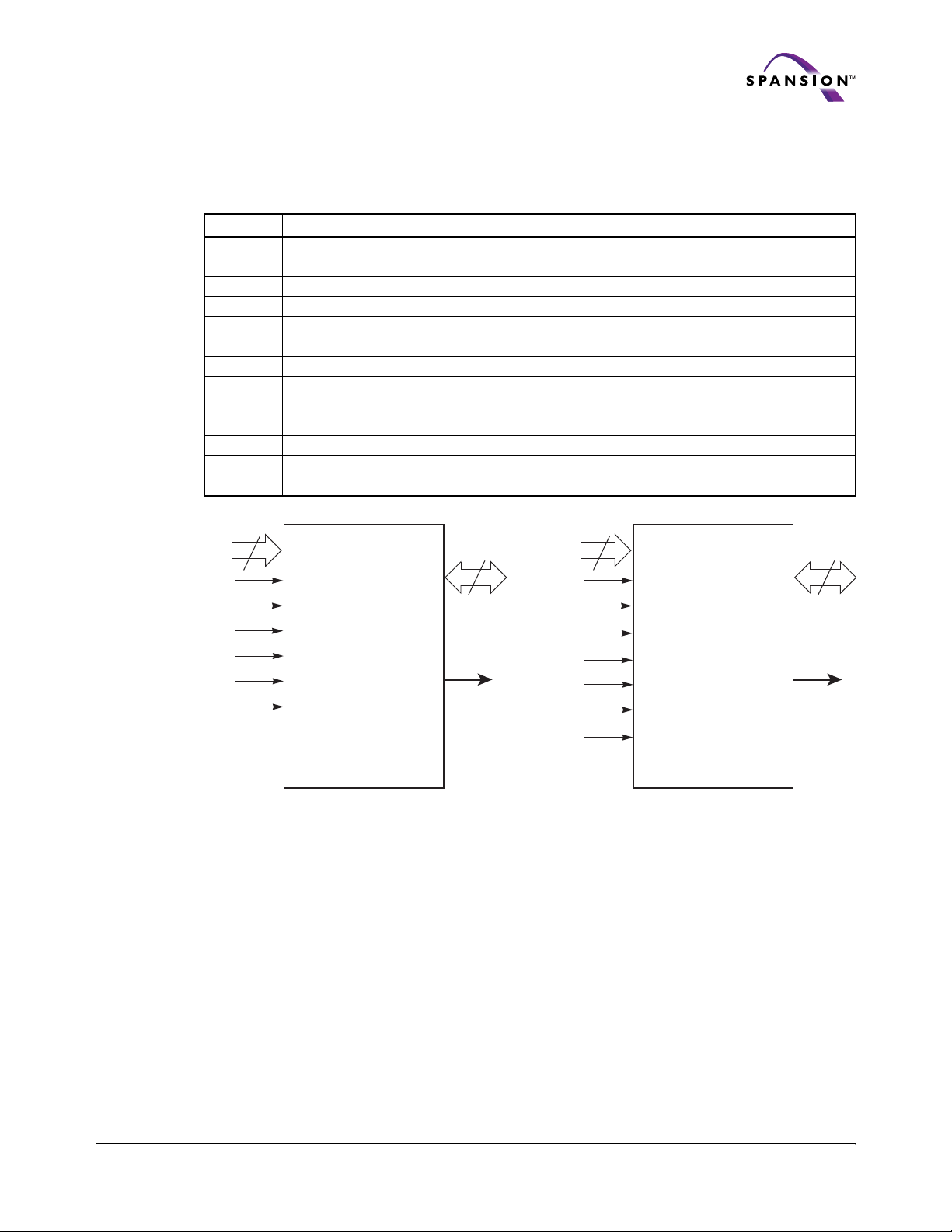
Table 2.1 identifies the input and output package connections provided on the device.
Table 2.1 Input/Output Descriptions
Symbol Ty p e Description
A
– A0 Input Address bus
max
DQ15 – DQ0 I/O 16-bit data inputs/outputs/float
CE# Input Chip Enable input
OE# Input Output Enable input
WE# Input Write Enable
V
SS
NC Not con ne cte d Pin Not Connected Internally
RY/BY# Output
V
CC
RESET# Input Hardware reset pin
CE1#, CE2# Input Chip Enable inputs for S29PL129 device
Supply Device ground
Ready/Busy output and open drain.
When RY/BY#= VIH, the device is ready to accept read operations and commands.
When RY/BY#= VOL, the device is either executing an embedded algorithm or the device
is executing a hardware reset operation.
Supply Device Power Supply
max +1
Amax–A0
CE#
DQ15 – DQ0
16
OE#
WE#
WP#/ACC
RESET#
RY/BY#
VCC
Notes:
1. Amax = 23 for the PL256N and 22 for the PL127N.
Figure 2.1 Logic Symbols – PL256N, PL129N, and PL127N
22
A21 – A0
CE1#
CE2#
OE#
WE#
WP#/ACC
RESET#
VCC
Logic Symbol – PL129NLogic Symbol – PL256N and PL127N
16
DQ15 – DQ0
RY/BY#
November 23, 2005 S29PL-N_00_A4 S29PL-N MirrorBit™ Flash Family 7
Page 10
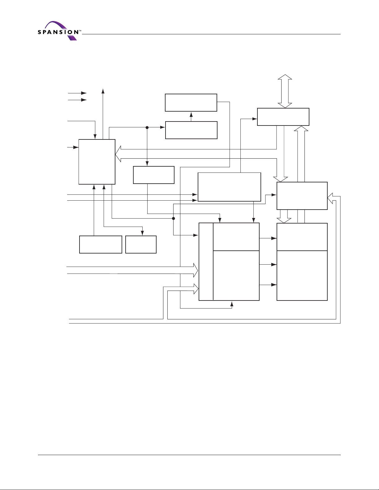
3 Block Diagram
Preliminary
DQ15–DQ0
V
CC
V
SS
RESET#
WE#
CE#
OE#
RY/BY# (See Note)
State
Control
Command
Register
PGM Voltage
Generator
VCC Detector Timer
Sector
Switches
Erase Voltage
Generator
Chip Enable
Output Enable
Logic
Y-Decoder
Input/Output
Buffers
Data Latch
Y-Gating
A
– A3
max
A2–A0
Notes:
1. RY/BY# is an open drain output.
2. A
3. PL129N has two CE# pins CE1# and CE2#.
= A23 (PL256N), A22 (PL127N), A21 (PL129N).
max
X-Decoder
Address Latch
Cell Matrix
8 S29PL-N MirrorBit™ Flash Family S29PL-N_00_A4 November 23, 2005
Page 11
Preliminary
r
4 Connection Diagrams/Physical Dimensions
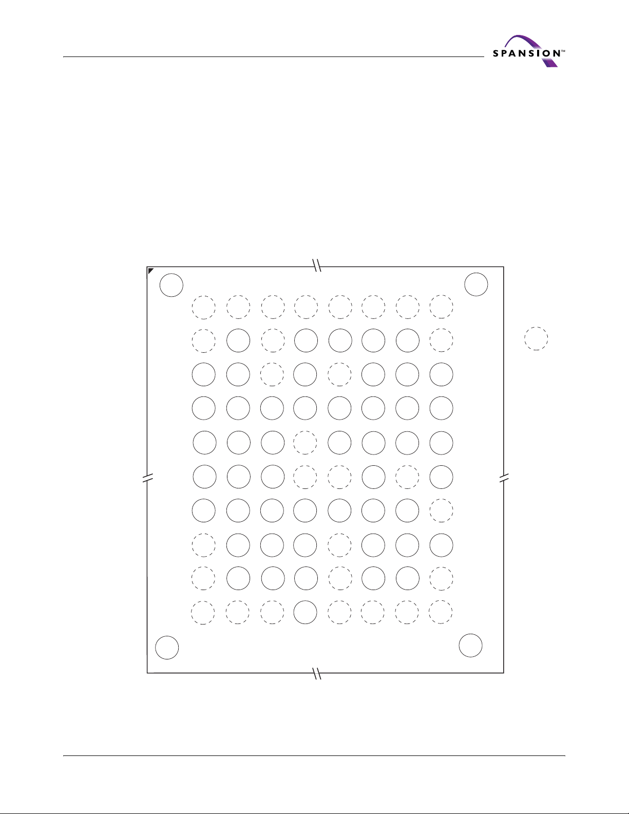
This section contains the I/O designations and package specifications for the S29PL256N.
4.1 Special Handling Instructions for FBGA Package
Special handling is required for Flash Memory products in FBGA packages.
Flash memory devices in FBGA packages may be damaged if exposed to ultrasonic cleaning meth -
ods. The package and/or data integrity may be compromised if the package body is exposed to
temperatures above 150°C for prolonged periods of time.
4.2 VBH084, 8.0 x 11.6 mm
4.2.1 Connection Diagram – S29PL256N MCP Compatible Package
M1
NC
A1
NC
B2 B9
RFU RFU
C2
RFU
D2 D3 D4 D5 D6 D7 D8 D9
A3
E2 E3 E4 E5 E6 E7 E8 E9
A2
F2 F3 F4 F7 F8 F9
A1 A4 A17 A10 A14 A22
H2 H3 H4 H5 H6 H7 H8 H9
CE#
J2 J3 J4 J5 J6 J7 J8
RFU
K2
RFU
RFU
B3 B4 B5 B6 B7 B8
RFU RFU RFU RFU RFU RFU
C3 C4 C5 C6 C7 C8
A7
A6 RFU RST# RFU A19 A12 A15
A5 A18 RY/BY# A20 A9 A13 A21
G3 G4G2 G7 G8 G9
V
OE# DQ9 DQ3 DQ4 DQ13 DQ15 RFU
DQ0
K3
DQ8
L3 L4 L5 L6 L7 L8
RFU RFU V
RFU WP#/ACC WE# A8 A11
F5
RFU A23
G5
DQ1A0 DQ6 RFU A16
SS
DQ10
DQ2
K4
RFU RFU
V
CC
K5
DQ11
F6
G6
RFU
K6
RFU
RFU RFU RFU
CC
DQ12 DQ7 V
K7
DQ5
K8
DQ14
RFU
J9
RFU
L9L2
RFU
A10
NC
Legend
C9
Reserved fo
Future Use
SS
K9
M10
NC
Notes:
1. Top view—balls facing down.
2. Recommended for wireless applications
Figure 4.1 Connection Diagram – 84-ball Fine-Pitch Ball Grid Array (S29PL256N)
November 23, 2005 S29PL-N_00_A4 S29PL-N MirrorBit™ Flash Family 9
Page 12
Preliminary
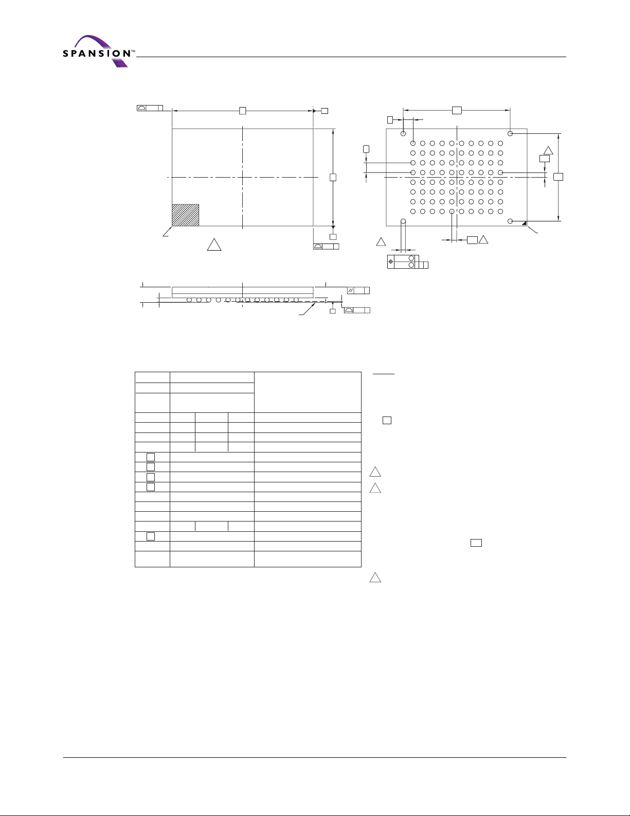
4.2.2 Physical Dimensions – VBH084, 8.0 x 11.6 mm
(2X)
C0.05
A1 CORNER
INDEX MARK
D
10
TOP VIEW
A
A1
SEATING PLANE
SIDE VIEW
PACKAGE VBH 084
JEDEC N/A
11.60 mm x 8.00 mm NOM
PACKAGE
SYMBOL MIN NOM MAX NOTE
A --- --- 1.00 OVERALL THICKNESS
A1 0.18 --- --- BALL HEIGHT
A2 0.62 --- 0.76 BODY THICKNESS
D 11.60 BSC. BODY SIZE
E 8.00 BSC. BODY SIZE
D1 8.80 BSC. BALL FOOTPRINT
E1 7.20 BSC. BALL FOOTPRINT
MD 12 ROW MATRIX SIZE D DIRECTION
ME 10 ROW MATRIX SIZE E DIRECTION
N 84 TOTAL BALL COUNT
φb 0.33 --- 0.43 BALL DIAMETER
e 0.80 BSC. BALL PITCH
SD / SE 0.40 BSC. SOLDER BALL PLACEMENT
(A2-A9, B10-L10, DEPOPULATED SOLDER BALLS
M2-M9, B1-L1)
Note: Recommended for wireless applications
A
D1
e
10
e
E
NXφb
ML JK
6
M
φ 0.08
C
M
φ 0.15
BCA
SD
7
BOTTOM VIEW
B
C0.05
(2X)
A2
0.10 C
C
C0.08
9
7
8
SE
7
6
E1
5
4
3
2
1
BACEDFHG
A1 CORNER
NOTES:
1. DIMENSIONING AND TOLERANCING PER ASME Y14.5M-1994.
2. ALL DIMENSIONS ARE IN MILLIMETERS.
3. BALL POSITION DESIGNATION PER JESD 95-1, SPP-010 (EXCEPT
AS NOTED).
4. e REPRESENTS THE SOLDER BALL GRID PITCH.
5. SYMBOL "MD" IS THE BALL ROW MATRIX SIZE IN THE
"D" DIRECTION.
SYMBOL "ME" IS THE BALL COLUMN MATRIX SIZE IN THE
"E" DIRECTION.
N IS THE TOTAL NUMBER OF SOLDER BALLS.
6 DIMENSION "b" IS MEASURED AT THE MAXIMUM BALL
DIAMETER IN A PLANE PARALLEL TO DATUM C.
7 SD AND SE ARE MEASURED WITH RESPECT TO DATUMS
A AND B AND DEFINE THE POSITION OF THE CENTER
SOLDER BALL IN THE OUTER ROW.
WHEN THERE IS AN ODD NUMBER OF SOLDER BALLS IN
THE OUTER ROW PARALLEL TO THE D OR E DIMENSION,
RESPECTIVELY, SD OR SE = 0.000.
WHEN THERE IS AN EVEN NUMBER OF SOLDER BALLS IN
THE OUTER ROW, SD OR SE = e/2
8. NOT USED.
9. "+" INDICATES THE THEORETICAL CENTER OF DEPOPULATED
BALLS.
10 A1 CORNER TO BE IDENTIFIED BY CHAMFER, LASER OR INK
MARK, METALLIZED MARK INDENTATION OR OTHER MEANS.
3339 \ 16-038.25b
Figure 4.2 Physical Dimensions – 84-ball Fine-Pitch Ball Grid Array (S29PL256N)
10 S29PL-N MirrorBit™ Flash Family S29PL-N_00_A4 November 23, 2005
Page 13

4.3 VBH064, 8 x 11.6 mm
H2
4.3.1 Connection Diagram – S29PL127N MCP Compatible Package
Preliminary
A1
NC
C3
A7
D2 D3
A6A3
E2 E3
A5A2
F2 F3
A4A1
G2 G3
A0
H2
H2
CE1#H3OE#
J2 J3
RFU DQ0
V
SS
B5
C4
D4
E4 E5
F4
A17
G4
DQ1
H4 H5 H6 H7 H8 H2
J4 J6 J7 J8 J9
DQ10
C5
D5
RST#RFU
RY/BY#A18
J5
CC
B7
RFURFU
C6 C7
D6
RFU
E6
A20
DQ12
C8
A8WE#WP/ACCRFU
D7 D8 D9
E7 E8 E9
F7 F8 F9
G7 G8 G9
A11
DQ7RFUV
A10
NC
Legend
Reserved for
Future Use
No Connection
A15A12A19
A21A13A9
A22A14A10
A16RFUDQ6
RFUDQ15DQ13DQ4DQ3DQ9
V
SS
K3
DQ8
M1
NC
K4 K5 K6 K7 K8
DQ14DQ5RFUDQ11DQ2
L5 L6
RFURFU
M10
NC
Notes:
1. Top view—balls facing down.
2. Recommended for wireless applications
Figure 4.3 Connection Diagram – 64-Ball Fine-Pitch Ball Grid Array (S29PL127N)
November 23, 2005 S29PL-N_00_A4 S29PL-N MirrorBit™ Flash Family 11
Page 14

Preliminary
H2
4.3.2 Connection Diagram – S29PL129N MCP Compatible Package
A1
NC
C3
A7
D2 D3
A6A3
E2 E3
A5A2
F2 F3
A4A1
G2 G3
A0
H2
H2
CE1#H3OE#
J2 J3
RFU DQ0
V
SS
B5
C4
D4
E4 E5
F4
A17
G4
DQ1
H4 H5 H6 H7 H8 H2
J4 J6 J7 J8 J9
DQ10
C5
D5
RST#RFU
RY/BY#A18
J5
CC
B7
RFURFU
C6 C7
D6
RFU
E6
A20
DQ12
C8
A8WE#WP/ACCRFU
D7 D8 D9
E7 E8 E9
F7 F8 F9
G7 G8 G9
A11
DQ7RFUV
A10
NC
Legend
Reserved for
Future Use
No Connection
A15A12A19
A21A13A9
CE2#A14A10
A16RFUDQ6
RFUDQ15DQ13DQ4DQ3DQ9
V
SS
K3
DQ8
M1
NC
K4 K5 K6 K7 K8
DQ14DQ5RFUDQ11DQ2
L5 L6
RFURFU
M10
NC
Notes:
1. Top view—balls facing down.
2. Recommended for wireless applications
Figure 4.4 Connection Diagram – 64-Ball Fine-Pitch Ball Grid Array (S29PL129N)
12 S29PL-N MirrorBit™ Flash Family S29PL-N_00_A4 November 23, 2005
Page 15
Preliminary
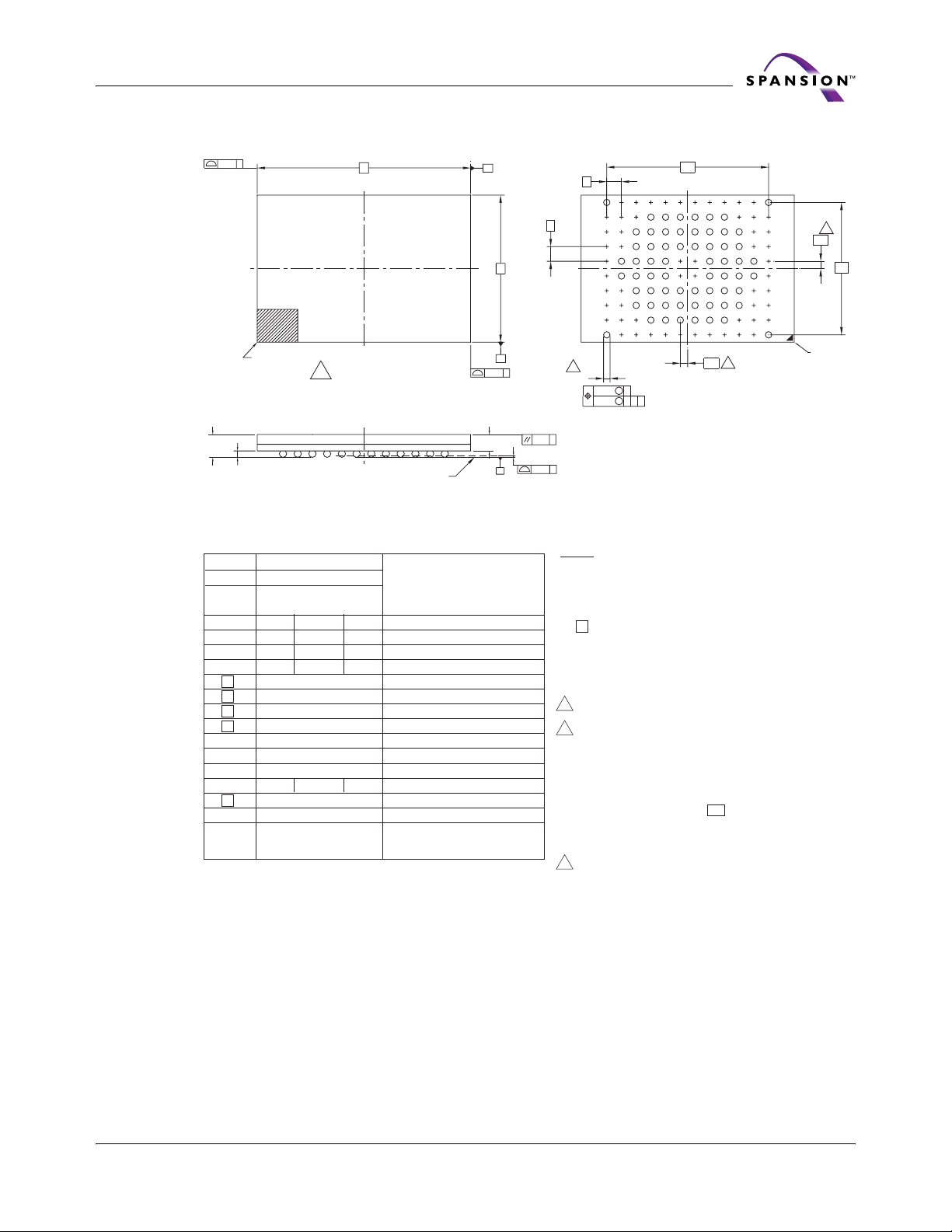
4.3.3 Physical Dimensions – VBH064, 8 x 11.6 mm – S29PL-N
(2X)
C0.05
A1 CORNER
INDEX MARK
D
10
TOP VIEW
A
A1
SEATING PLANE
SIDE VIEW
PACKAGE VBH 064
JEDEC N/A
11.60 mm x 8.00 mm NOM
PACKAGE
SYMBOL MIN NOM MAX NOTE
A --- --- 1.00 OVERALL THICKNESS
A1 0.18 --- --- BALL HEIGHT
A2 0.62 --- 0.76 BODY THICKNESS
D 11.60 BSC. BODY SIZE
E 8.00 BSC. BODY SIZE
D1 8.80 BSC. BALL FOOTPRINT
E1 7.20 BSC. BALL FOOTPRINT
MD 12 ROW MATRIX SIZE D DIRECTION
ME 10 ROW MATRIX SIZE E DIRECTION
N 64 TOTAL BALL COUNT
φb 0.33 --- 0.43 BALL DIAMETER
e 0.80 BSC. BALL PITCH
SD / SE 0.40 BSC. SOLDER BALL PLACEMENT
(A2-9,B1-4,B7-10,C1-K1, DEPOPULATED SOLDER BALLS
M2-9,C10-K10,L1-4,L7-10,
G5-6,F5-6)
Note: Recommended for wireless applications
A
D1
e
10
9
7
8
SE
7
6
E1
5
4
3
2
1
BACEDFHG
A1 CORNER
(2X)
e
E
B
C0.05
6
NXφb
ML JK
φ 0.08
φ 0.15
SD
7
M
C
M
BCA
BOTTOM VIEW
A2
0.10 C
C
C0.08
NOTES:
1. DIMENSIONING AND TOLERANCING PER ASME Y14.5M-1994.
2. ALL DIMENSIONS ARE IN MILLIMETERS.
3. BALL POSITION DESIGNATION PER JESD 95-1, SPP-010 (EXCEPT
AS NOTED).
4. e REPRESENTS THE SOLDER BALL GRID PITCH.
5. SYMBOL "MD" IS THE BALL ROW MATRIX SIZE IN THE
"D" DIRECTION.
SYMBOL "ME" IS THE BALL COLUMN MATRIX SIZE IN THE
"E" DIRECTION.
N IS THE TOTAL NUMBER OF SOLDER BALLS.
6 DIMENSION "b" IS MEASURED AT THE MAXIMUM BALL
DIAMETER IN A PLANE PARALLEL TO DATUM C.
7 SD AND SE ARE MEASURED WITH RESPECT TO DATUMS
A AND B AND DEFINE THE POSITION OF THE CENTER
SOLDER BALL IN THE OUTER ROW.
WHEN THERE IS AN ODD NUMBER OF SOLDER BALLS IN
THE OUTER ROW PARALLEL TO THE D OR E DIMENSION,
RESPECTIVELY, SD OR SE = 0.000.
WHEN THERE IS AN EVEN NUMBER OF SOLDER BALLS IN
THE OUTER ROW, SD OR SE = e/2
8. NOT USED.
9. "+" INDICATES THE THEORETICAL CENTER OF DEPOPULATED
BALLS.
10 A1 CORNER TO BE IDENTIFIED BY CHAMFER, LASER OR INK
MARK, METALLIZED MARK INDENTATION OR OTHER MEANS.
3330 \ 16-038.25b
Figure 4.5 Physical Dimensions – 64-Ball Fine-Pitch Ball Grid Array (S29PL-N)
November 23, 2005 S29PL-N_00_A4 S29PL-N MirrorBit™ Flash Family 13
Page 16
Preliminary
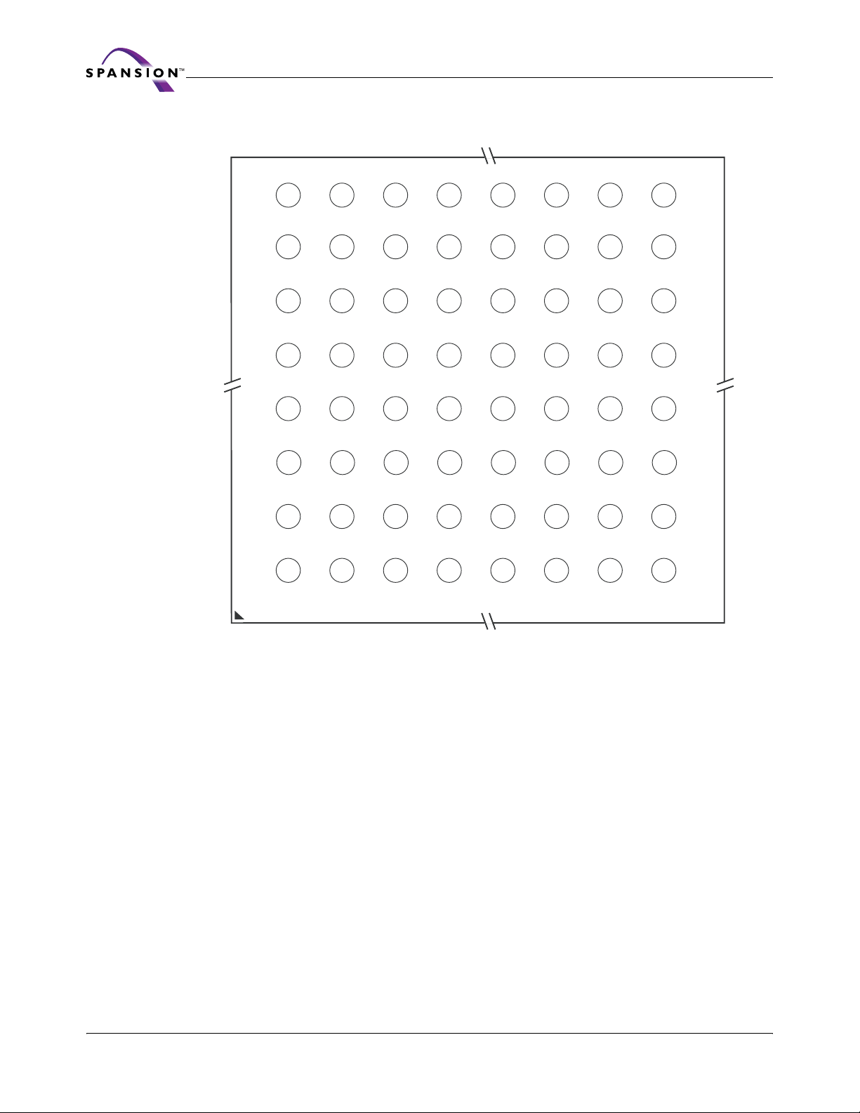
4.3.4 Connection Diagram – S29PL-N Fortified Ball Grid Array Package
A8 C8
A7 C7 D7 E7 F7 G7 H7
A6 C6 D6 E6 F6 G6 H6
A5 C5 D5 E5 F5 G5 H5
A4 C4 D4 E4 F4 G4 H4
A3 C3 D3 E3 F3 G3 H3
A2 C2 D2 E2 F2 G2 H2
A1 C1 D1 E1 F1 G1 H1
B8 D8 E8 F8 G8 H8
NC
V
V
NC
B7
B6
B5
B4
B3
B2
B1
A23A22NC
A18WP#/ACCRY/BY#
V
CC
SS
NCV
RFUA16A15A14A12A13
CE#A0A1A2A4A3
RFUNCNCNCNCNC
NC
DQ15
DQ13 DQ6DQ14DQ7A11A10A8A9
V
CC DQ4DQ12DQ5A19A21RESET#WE#
DQ11 DQ3DQ10DQ2A20
DQ9 DQ1DQ8DQ0A5A6A17A7
OE#
NC
SS
SS
Notes:
1. Top view—balls facing down.
2. A23 is NC on PL127N.
Figure 4.6 Connection Diagram – 64-Ball Fine-Pitch Ball Grid Array (S29PL127N, S29PL256N)
14 S29PL-N MirrorBit™ Flash Family S29PL-N_00_A4 November 23, 2005
Page 17
Preliminary
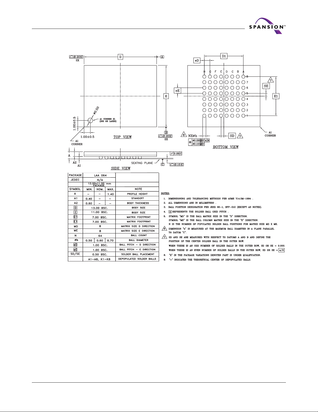
4.3.5 Physical Dimensions – LAA064, 11 x 13 mm – S29PL-N
Note: Recommended for automotive applications
Figure 4.7 Physical Dimensions – 64-Ball Fortified Ball Grid Array (S29PL-N)
November 23, 2005 S29PL-N_00_A4 S29PL-N MirrorBit™ Flash Family 15
Page 18
Preliminary
C6C6
L2
XX
XX
XX
XX
XX
XX
G5G5
H5H5
H6H6
C7C7
C8C8
C9C9
D9D9
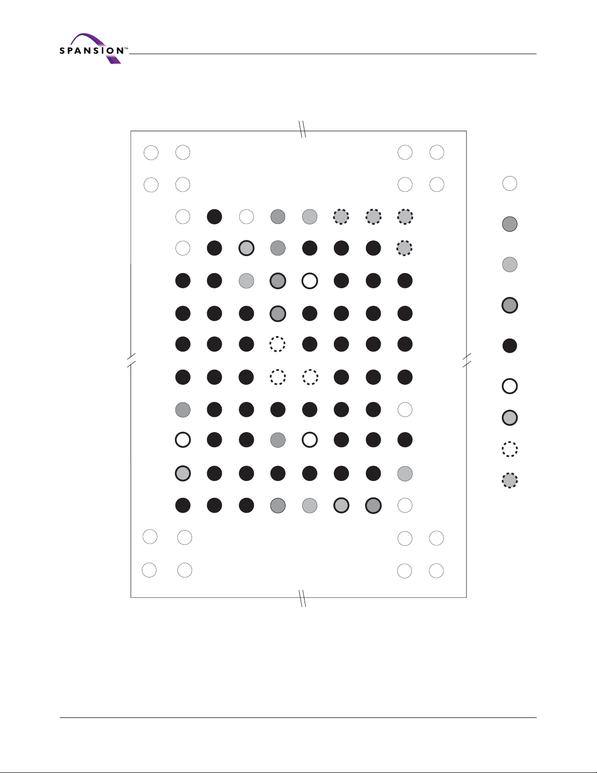
4.4 MCP Look-Ahead Connection Diagram/Physical Dimensions
4.4.1 For All Page Mode MCPs Comprised of Code Flash + (p)SRAM + Data Flash
A1
NC
B1
NC
A2
NC
B2
NC
C2
RFU
D2
RFU
E2
A3
F2F2
A2
G2G2
A1
H2H2
A0
J2J2
F1-CE#
K2
R1-CE1# F-V
L2
L2
R1-V
C3
V
SS
D3
A7
E3
A6
F3F3
A5
G3G3
A4
H3H3
V
SS
J3
OE#
K3K3
DQ0
L3L3
DQ8
CC
M2
A27M3A26
N1
NC
N2
NC
C4
RFU
D4
R-LB#
E4
R-UB#
F4F4
A18
G4G4
A17
H4H4
DQ1
J4
DQ9
K4K4
DQ10
L4L4
DQ2
M4
V
SS
C5C5
F2-CE# N-CLE
D5D5
WP#/ACC
E5E5
F-RST#
F5F5
F-RY/BY#
G5G5
R2-CE1# or
(N-WE#)
H5H5
R2-V
(or N-VCC)
J5
DQ3
F-VCC or
R1-CE2
R2-CE2 or
CC
(N-RE#)
(N-V
D6
WE#
A20
G6G6
A23
DQ4
C6C6
E6
F6F6
H6H6
J6
C7C7
)
CC
D7
A8
E7
A19
F7F7
A9
G7G7
A10
H7
DQ6
J7
DQ13
N-ALE#N-PRE
D8
A11
A12
A13
G8G8
A14
H8
A24
DQ15
C8C8
N1-CE#
E8
F8F8
J8
K5K5
L5L5
DQ11
M5M5 M8M8
F-V
CC
CC
K6
R1-V
L6L6
A25
M6
N2-CE#
K7K7
DQ12
CC
L7L7
DQ5
M7
R-V
CCQ
K8K8
DQ7
L8L8
DQ14
F-V
N-WP#
IO
A9
NC
B9
NC
C9C9
D9D9
E9
A15
F9F9
A21
G9G9
A22
H9
A16
J9
RFU
K9K9
V
SS
L9
M9
RFU
N9
NC
A10
NC
B10
NC
N10
NC
Legend:
X
RFU
(Reserved for
Future Use)
X
Code Flash Only
X
MirrorBit Data
Only
X
Flash/Data
Shared
X
Flash/xRAM
Shared
X
pSRAM Only
X
xRAM Shared
X
NAND or pSRAM
X
NAND
P1
NC
Notes:
1. F1 and F2 denote XIP/Code Flash, while F3 and F4 denote Data/Companion Flash.
2. In addition to being defined as F2-CE#, Ball C5 can also be assigned as F1-CE2# for code flash that has two chip enable
signals.
3. F-VIO is RFU on the PL-N product family.
P2
NC
P9
NC
P10
NC
Figure 4.8 MCP Look-Ahead Diagram
16 S29PL-N MirrorBit™ Flash Family S29PL-N_00_A4 November 23, 2005
Page 19

Preliminary
To provide cu stomers with a migration path to higher densities, as well as the option to stack
more die in a package, Spansion has prepared a standard pinout that supports:
NOR Flash and SRAM densities up to 4 Gb
NOR Flash and PSRAM densities up to 4 Gb
NOR Flash and PSRAM and Data Storage densities up to 4 Gb
The signal locations of the resultant MCP device are shown above. Note that for different densities, the actual package outline can vary . However, any pinout in any MCP is a subset of the pinout
shown above.
In some cases, there may be outrigger balls in locations outside the grid shown above. In such
cases, the user is advised to treat these as RFUs, and not connect them to any other signal.
In case of any further inquiries about the above look-ahead pinout, please see the application
note, Design-in Scalable Wireless Solutions with Spansion Products, or contact a Spansion sales
office.
November 23, 2005 S29PL-N_00_A4 S29PL-N MirrorBit™ Flash Family 17
Page 20

5 Additional Resources
Visit www.amd.com and www.fujitsu.com to obtain the following related documents:
Application Notes
Using the Operation Status Bits in AMD Devices
Simultaneous Read/Write vs. Erase Suspend/Resume
MirrorBit™ Flash Memory Write Buffer Programming and Page Buffer Read
Design-In Scalable Wireless Solutions with Spansion Products
Common Flash Interface Version 1.4 Vendor Specific Extensions
Specification Bulletins
Contact your local sales office for details.
Drivers and Software Support
Spansion Low-Level Drivers
Enhanced Flash Drivers
Flash File System
CAD Modeling Support
VHDL and Verilog
IBIS
ORCAD
Preliminary
Technical Support
Contact your local sales office or contact Spansion LLC directly for additional technical support:
Email
US and Canada: [email protected]
Asia Pacific: [email protected]
Europe, Middle East, and Africa
Japan: http://edevice.fujitsu.com/jp/support/tech/#b7
Frequently Asked Questions (FAQ)
http://ask.amd.com/
http://edevice.fujitsu.com/jp/support/tech/#b7
Phone
US: (408) 749-5703
Japan (03) 5322-3324
Spansion LLC Locations
915 DeGuigne Drive, P.O. Box 3453
Sunnyvale, CA 94088-3453, USA
Telephone: 408-962-2500 or
1-866-SPANSION
Spansion Japan Limited
4-33-4 Nishi Shinjuku, Shinjuku-ku
Tokyo, 160-0023
Telephone: +81-3-5302-2200
Facsimile: +81-3-5302-2674
http://www.spansion.com
18 S29PL-N MirrorBit™ Flash Family S29PL-N_00_A4 November 23, 2005
Page 21
6 Product Overview
The S29PLxxxN family consists of 256 and 128 Mb, 3.0 volts-only, simultaneous read/write
page-mode read Flash devices that are optimized for wireless designs of toda y that demand large
storage array and rich functionality, while requiring low power consumption. These products also
offer 32-word buffer for progr amming with progr am and erase suspend/resume functionality. Ad
ditional features include:
Advanced Sector Protection methods for protecting an individual or group of sectors as re-
quired,
256-word of secured silicon area for storing customer and factory secured information
Simultaneous Read/Write operation
6.1 Memory Map
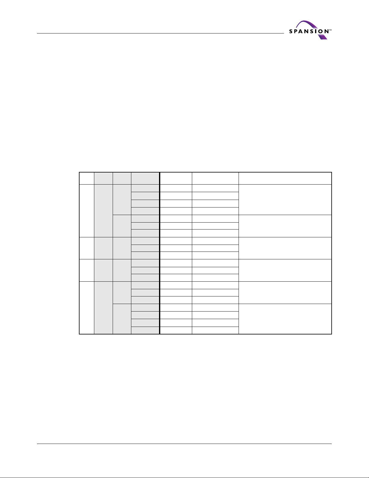
The S29PL -N devices consist of 4 banks organized as shown in Tables 6.1, 6.2, and 6.3.
Bank
Size
4 MB
4 MB
Sector
Count
4
15
15
4
Bank
A
12 MB 48
B
C
12 MB 48
D
Note: Ellipses indicate that o th er addresses in sector range follow the same pa tt ern .
Preliminary
Table 6.1 PL256N Sector and Memory Address Map
Sector Size
(KB)
64 SA00 000000h-007FFFh
64 SA01 008000h-00FFFFh
64 SA02 010000h-017FFFh
64 SA03 018000h-01FFFFh
256 SA04 020000h-03FFFFh
…
256 SA018 1E0000h-1FFFFFh
256 SA19 200000h-21FFFFh
…
256 SA66 7E0000h-7FFFFFh
256 SA67 800000h-81FFFFh
…
256 SA114 DE0000h-DFFFFFh
256 SA115 E00000h-E1FFFFh
…
256 SA129 FC0000h-FDFFFFh
64 SA130 FE0000h-FE7FFFh
64 SA131 FE8000h-FEFFFFh
64 SA132 FF0000h-FF7FFFh
64 SA133 FF8000h-FFFFFFh
Sector/
Sector Range
…
…
…
…
Address Range Notes
Sector Starting Address –
Sector Ending Address
Sector Starting Address -
…
…
…
…
Sector Ending Address
First Sector, Secto r Starting Address -
Last Sector, Sector Ending Address
First Sector, Secto r Starting Address -
Last Sector, Sector Ending Address
Sector Starting Address -
Sector Ending Address
Sector Starting Address -
Sector Ending Address
-
(see note)
(see note)
(see note)
(see note)
November 23, 2005 S29PL-N_00_A4 S29PL-N MirrorBit™ Flash Family 19
Page 22
Preliminary
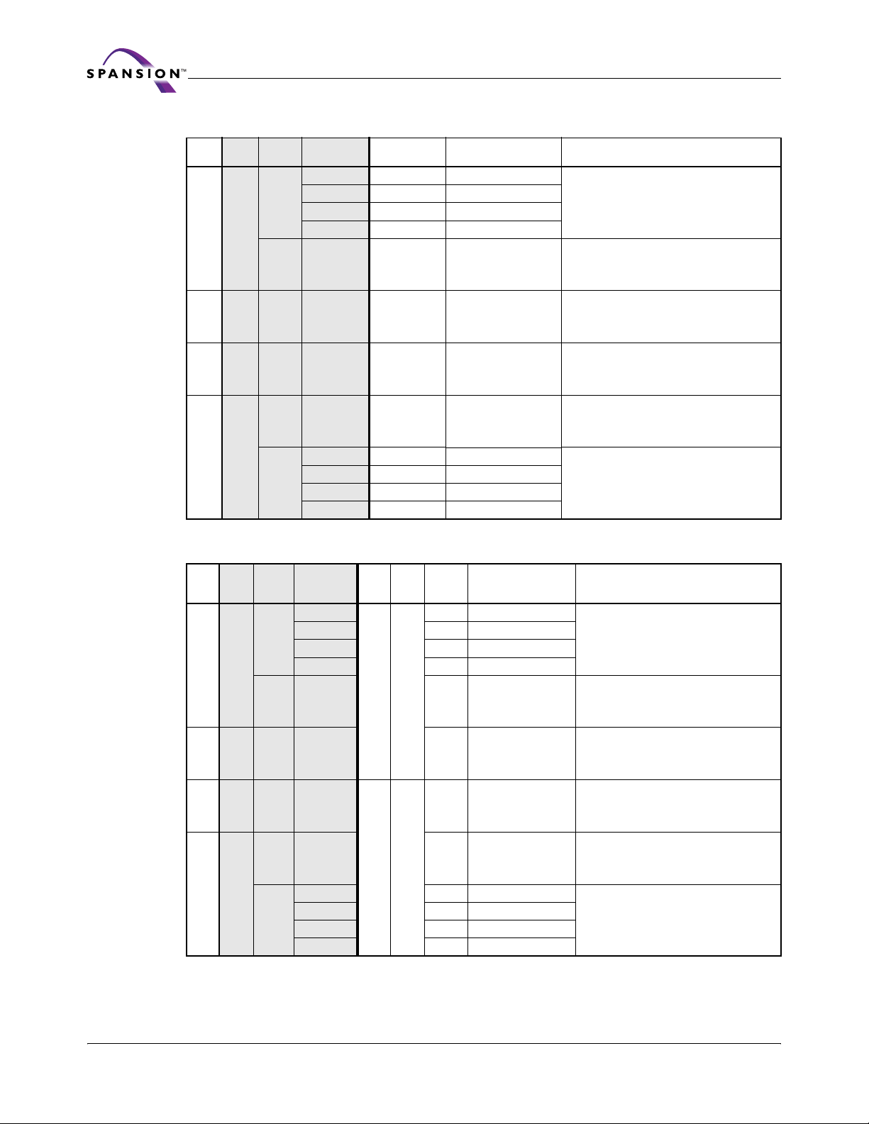
Table 6.2 PL127N Sector and Memory Address Map
Bank
Bank
A
B
C
D
Sector
Size
Count
2 MB
6 MB 24
6 MB 24
2 MB
4
7
7
4
Sector Size
(KB)
64 SA00 000000h-007FFFh
64 SA01 008000h-00FFFFh
64 SA02 010000h-017FFFh
64 SA03 018000h-01FFFFh
256 SA04 020000h-03FFFFh
…
256 SA10 0E0000h-0FFFFFh
256 SA11 100000h-11FFFFh
…
256 SA34 3E0000h-3FFFFFh
256 SA35 400000h-41FFFFh
…
256 SA58 6E0000h-6FFFFFh
256 SA59 700000h-71FFFFh
…
256 SA65 7C0000h-7DFFFFh
64 SA66 7E0000h-7E7FFFh
64 SA67 7E80000h-7EFFFFh
64 SA68 7F0000h-7F7FFFh
64 SA69 7F8000h-7FFFFFh
Sector/
Sector Range
…
…
…
…
Address Range Notes
…
…
…
…
First Sector, Sector Starting Address -
First Sector, Sector Starting Address -
Note: Ellipses indicate that o th er addresses in sector range follow the same pa tt ern .
Table 6.3 PL129N Sector and Memory Address Map
Bank
1A
1B
2A
2B
Bank
Sector
Size
Count
2 MB
6 MB 24
6 MB 24
2 MB
4
7
7
4
Sector Size
(KB)
256 SA04 020000h-03FFFFh
256 SA10 0E0000h-0FFFFFh
256 SA11 100000h-11FFFFh
256 SA34 3E0000h-3FFFFFh
256
256 SA58 2E0000h - 2FFFFFh
256 SA59 300000h-31FFFFh
256 SA65 3C0000h-3DFFFFh
CE1# CE2#
64
64 SA01 008000h-00FFFFh
64 SA02 010000h-017FFFh
64 SA03 018000h-01FFFFh
V
…
…
…
…
64 SA66 3E0000h-3E7FFFH
64 SA67 3E8000h-3EFFFFh
64 SA68 3F0000h-3F7FFFh
64 SA69 3F8000h-3FFFFFh
ILVIH
V
IHVIL
Sector/
Sector
Range
SA00 000000h-007FFFh
SA35 000000h-01FFFFh
Address Range Notes
…
…
…
…
…
…
…
…
Sector Starting Address -
Sector Ending Address
Sector Starting Address –
Sector Ending Address
(see note)
Last Sector, Sector Ending Address
Last Sector, Sector Ending Address
First Sector, Sector Starting Address -
Last Sector, Secto r Ending Address
First Sector, Sector Starting Address -
Last Sector, Secto r Ending Address
(see note)
(see note)
Sector Starting Address -
Sector Ending Address
(see note)
Sector Starting Address -
Sector Ending Address
Sector Starting Address -
Sector Ending Address
Sector Starting Address –
Sector Ending Address
(see note)
(see note)
(see note)
Sector Starting Address -
Sector Ending Address
(see note)
Sector Starting Address -
Sector Ending Address
20 S29PL-N MirrorBit™ Flash Family S29PL-N_00_A4 November 23, 2005
Page 23
Preliminary
7 Device Operations
This section describes the read, program, erase, simultaneous read/write operations, and reset
features of the Flash devices.
Operations are initiated by writing specific commands or a sequence with specific address and
data patterns into the command registers (see
ter itself does not occupy any addressable memory location. Instead, the command register is
composed of latches that store the commands, along with the address and data information
needed to execute the command. The contents of the register serve as input to the inter nal state
machine and the state machine outputs dictate the function of the device. Writing incorrect ad
dress and data values or writing them in an improper sequence can place the device in an
unknown state, in which case the system must write the reset command to return the device to
the reading array data mode.
7.1 Device Operation Table
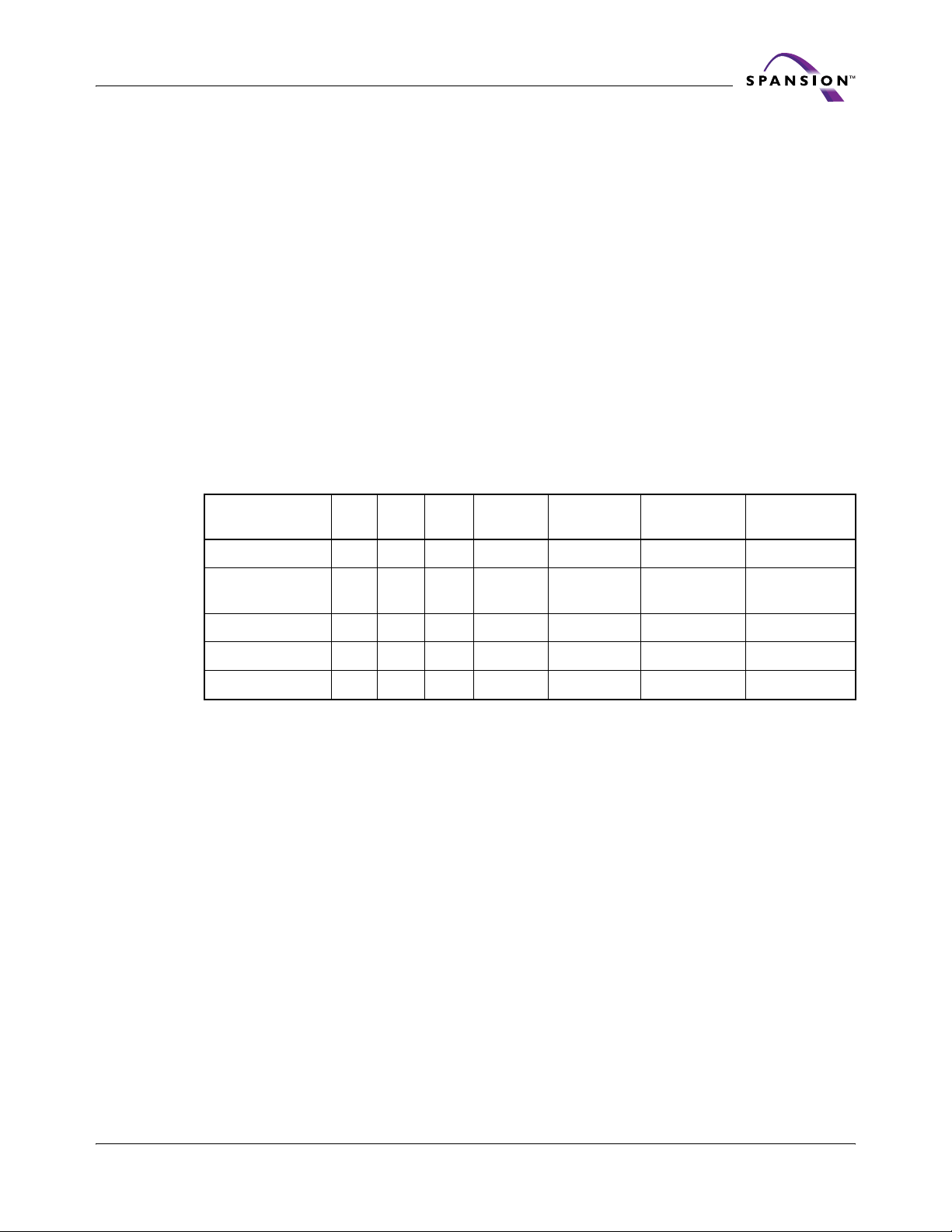
The device must be setup appropriately for each operation. Table 7.1 describes the required state
of each control pin for any particular operation.
Operation CE# OE# WE# RESET# WP#/ACC
Read L L H H X A
Write L H L H
Table 12.1 and Table 12.2). The command regis-
Table 7.1 Device Operation
X
(See Note)
Addresses
(A
– A0) DQ15 – DQ0
max
IN
A
IN
-
D
OUT
D
IN
Standby H X X H X A
Output Disable L H H H X A
Reset X X X L X A
Legend: L = Logic Low = VIL, H = Logic High = VIH, VHH = 8.5 – 9.5 V, X = Don’t Care, SA = Sector Address, AIN = Address
= Data In, D
In, D
IN
Note: WP#/ACC must be high when writing to upper two and lower two sectors (PL256N: 0, 1,132, and 133; PL127/129N:
0, 1, 68, and 69)
= Data Out
OUT
IN
IN
IN
7.1.1 Dual Chip Enable Device Description and Operation (PL129N Only)
The dual CE# product (PL129N) offers a reduced number of address pins to accommodate processors with a limited addressable range. This product operates as two separate devices in a
single package and requires the processor to address half of the memory space with one chip en
able and the remaining memory space with a second chip enable. For more details on the
addressing features of the Dual CE# device refer to
and Memory Address Map.
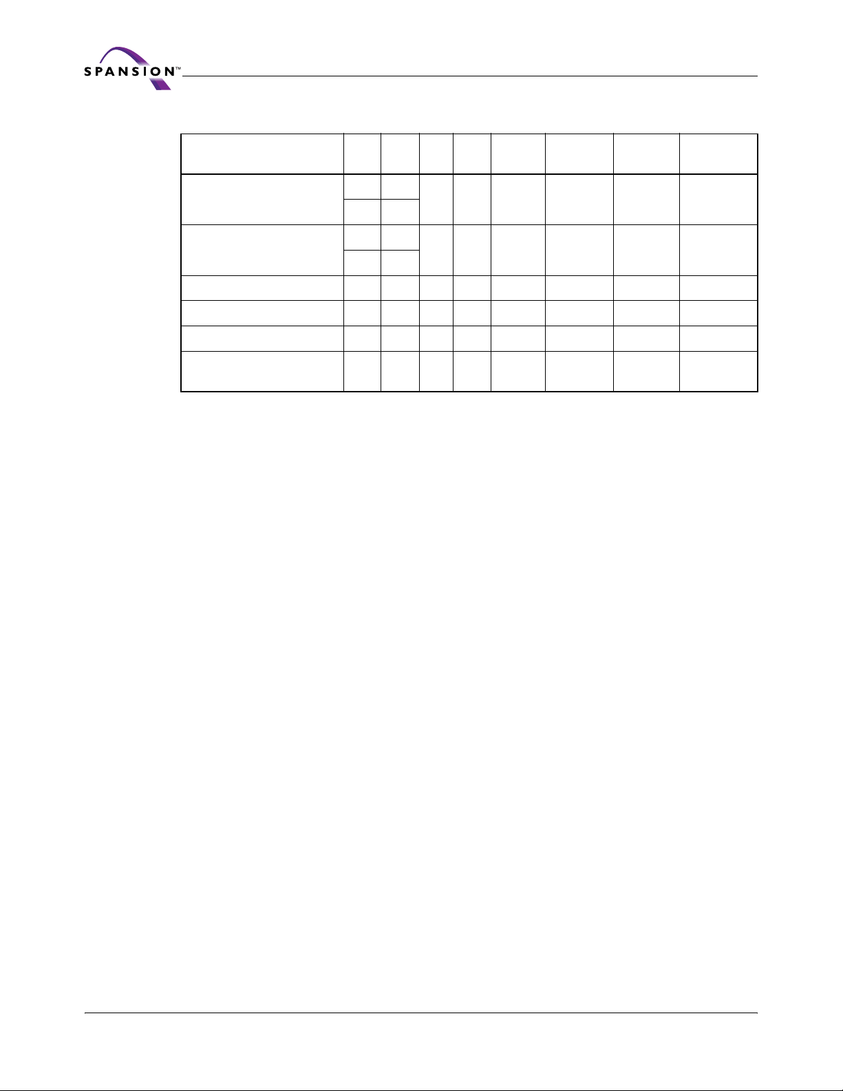
Dual chip enable products must be setup appropriately for each operation. To place the device
into the active state either CE1# or CE2# must be set to V
both CE1# and CE2# must be set to V
. Table 7.2 describes the required state of each control
IH
pin for any particular operation.
Table 6.3 on page 20 for the PL129N Sector
. T o place the device in standby mode,
IL
High-Z
High-Z
High-Z
-
November 23, 2005 S29PL-N_00_A4 S29PL-N MirrorBit™ Flash Family 21
Page 24
Preliminary
Table 7.2 Dual Chip Enable Device Operation
Operation CE1# CE2# OE# WE# RESET# WP#/ACC
Addresses
(A21 – A0) DQ15 – DQ0
Read
Write
Standby H H X X H X X High-Z
Output Disable L L H H H X X High-Z
Reset X X X X L X X High-Z
Temporary Sector Unprotect
(High Voltage)
Legend: L = Logic Low = VIL, H = Logic High = VIH,VID = 11.5–12.5 V, VHH = 8.5 – 9.5 V,
X = Don’t Care, SA = Sector Address, AIN = Address In, DIN = Data In, D
Notes:
1. The sector and sector unprotect functions may also be implemented by programming equipment.
2. WP#/ACC must be high when writing to the upper two and lower two sectors.
7.2 Asynchronous Read
The internal state machine is set for reading array data upon device power-up, or after a hardware
reset. This ensures that no spurious alteration of the memory content occurs during the power
transition. No command is necessary in this mode to obtain array data. Standard microprocessor
read cycles that assert valid addresses on the device address inputs produce valid data on the
device data outputs. Each bank remains enabled for read access until the command register con
tents are altered.
LH
LH H X
HL
LH
HL H
HL
XXXX V
ID
OUT
X
(Note 2)
X
= Data Out
A
IN
A
IN
A
IN
D
OUT
D
IN
D
IN
-
7.2.1 Non-Page Random Read
Address access time (t
chip enable access time (t
at the output inputs. The output enable access time is the delay fr om the falling edge of the OE#
to valid data at the output (assuming the addresses have been stable for at least t
) is equal to the delay from stable addresses to valid output data. The
ACC
) is the delay from the stable addresses and stable CE# to valid data
CE
7.2.2 Page Mode Read
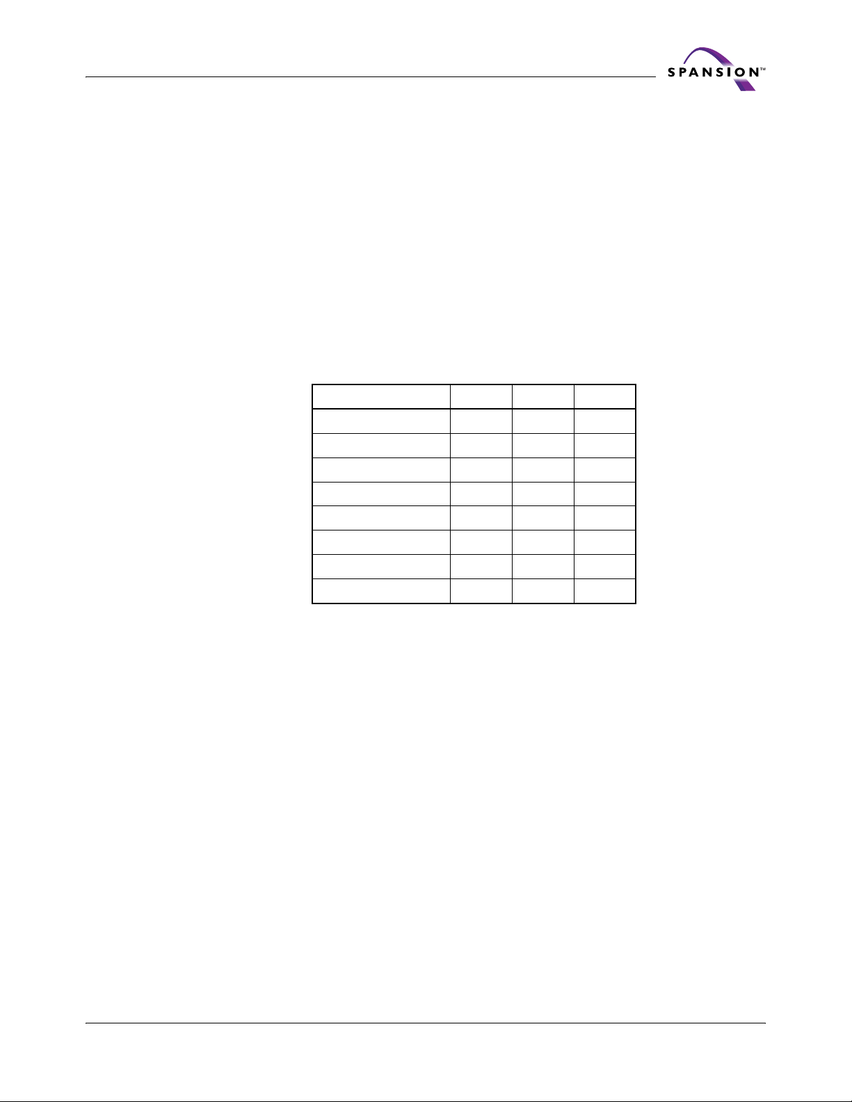
The device is capable of fast page mode read and is compatible with the page mode Mask ROM
read operation. This mode provides faster read access speed for random locations within a page.
The random or initial page access is t
the locations specified by the microprocessor falls within that page) is equivalent to t
CE# is deasserted (=
or tCE. Here again, CE# selects the device and OE# is the output control and should be used to
gate data to the output inputs if the device is selected. F ast page mode accesses are obtained b y
keeping A
– A3 constant and changing A2 – A0 to select the specific word wit hin that page.
max
Address bits A
within that page. This is an asynchronous operation with the microprocessor supplying the specific
word location. See
VIH), the reassertion of CE# for subsequent access has access time of t
– A3 select an 8-word page, and address bits A2 – A0 select a specific word
max
Table 7.3 for details on selecting specific words.
– tOE time).
ACC
or tCE and subsequent page read accesses (as long as
ACC
PACC
. When
ACC
22 S29PL-N MirrorBit™ Flash Family S29PL-N_00_A4 November 23, 2005
Page 25
Preliminary
The device is automatically set to reading array data after device power-up. No commands are
required to retrieve data. Each bank is ready to read array data after completing an Embedded
Program or Embedded Erase algorithm. All addresses are latched on the falling edge of WE# or
CE#, whichever happens later. All data is latched on the rising edge of WE# or CE#, whichever
happens first.
Reads from the memory arra y may be performed in conjunction with the Erase Suspend and Program Suspend features. After the device accepts an Erase Suspend command, the corresponding
bank enters the erase-suspend-read mode, after which the system can read data from any nonerase-suspended sector within the same bank. The system can read array data using the standard
read timing, except that if it reads at an address within erase-suspended sectors, the device out
puts status data. After completing a programming operation in the Erase Suspend mode, the
system may once again read array data with the same ex ception. After the device accepts a Pro
gram Suspend command, the corresponding bank enters the program-suspend-read mode, a fter
which the system can read data from any non-program-suspended sector within the same bank.
Table 7.3 Word Selection within a Page
Word A2 A1 A0
Word 0 0 0 0
Word 1 0 0 1
Word 2 0 1 0
-
-
7.3 Autoselect
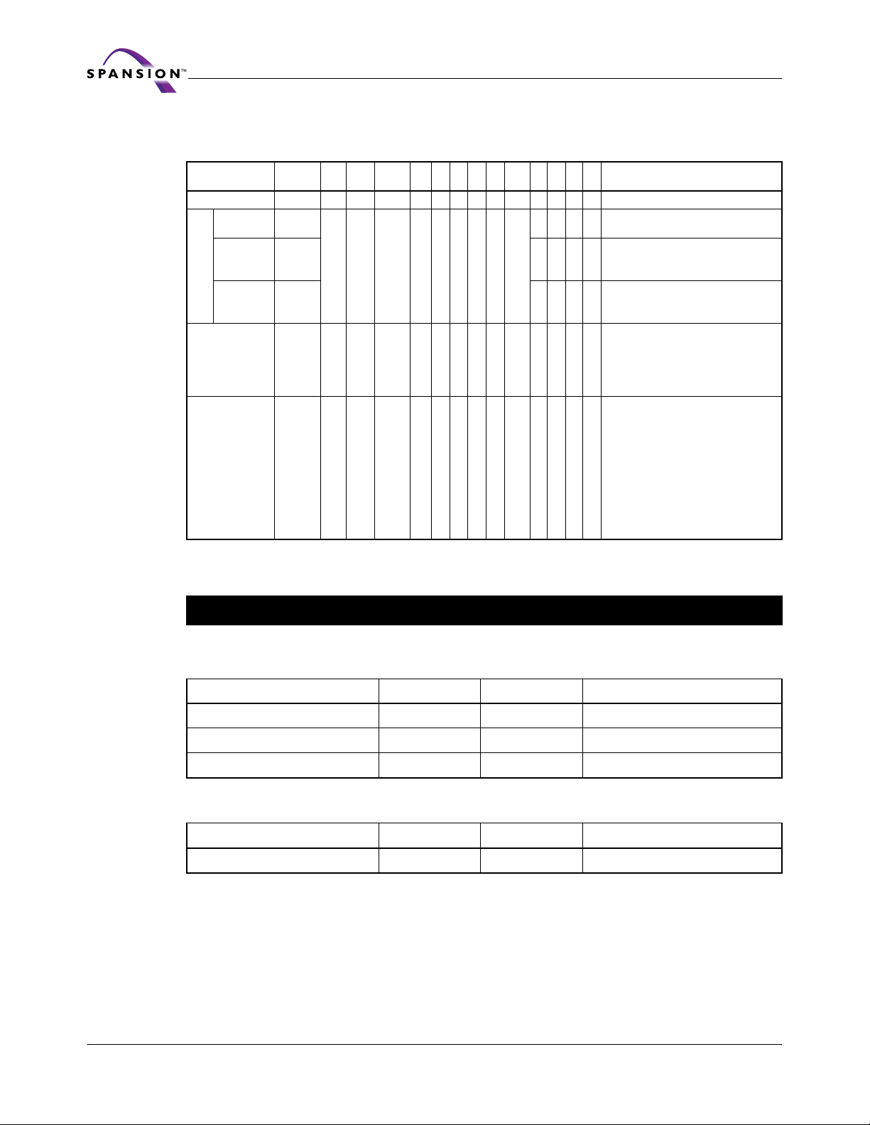
The Autoselect mode allows the host system to access manufacturer and device identification,
and verify sector protection, through identifier codes output from the internal register (separate
from the memory array) on DQ15-DQ0. This mode is primarily intended to allow equipment to
automatically match a device to be programmed with its corresponding programming algorithm.
When verifying sector protection, the sector address must appear on the appropriate highest
order address bits (see
bits have been set as required, the programming equipment can then read the corresponding
identifier code on DQ15-DQ0.
The Autoselect codes can also be accessed in-system through the command register. Note that if
a Bank Address (BA) on the four uppermost address bits is asserted during the third write cycle
of the Autoselect command, the host system can read Autoselect data from that bank and then
immediately read array data fr om the other bank, without exiting the Autoselect mode.
To access the Autoselect codes, the host system must issue the Autoselect command.
The Autoselect command sequence can be written to an address within a bank that is either
in the read or erase-suspend-read mode.
The Autoselect command cannot be written while the device is actively programming or er as-
ing in the other bank.
Autoselect does not support simultaneous operations or page modes.
The system must writ e the reset command to return to the read mode (or erase-suspend-
read mode if the bank was previously in Erase Suspend).
Word 3 0 1 1
Word 4 1 0 0
Word 5 1 0 1
Word 6 1 1 0
Word 7 1 1 1
Table 7.5). The remaining address bits are don't care. When all necessary
November 23, 2005 S29PL-N_00_A4 S29PL-N MirrorBit™ Flash Family 23
Page 26
Preliminary
See Table 12.1 for command sequence details.
Description
Manufacturer ID L L H BA X X X L L X L L L L 0001h
Read
Cycle 1
Read
Cycle 2
Device ID:
Read
Cycle 3
Sector
Protection
Verification
Indicator Bit L L H BA X X X L L L L L H H
CE#
See Note
OE# WE#
L
LHHHL
LHBAXXXLLL
L HHHH
LLHSAXXXLLLLLHL
Table 7.4 Autoselect Codes
A
–
max
A10 A9 A8 A7 A6
A12
A5 –
A3 A2 A1 A0 DQ15 to DQ0
A4
L L L H 227Eh
223Ch (PL256N)
2220h (PL127N)
2221h (PL129N)
2200h (PL256N)
2200h (PL127N)
2200h (PL129N)
0000h
Unprotected
(Neither DYB nor PPB Locked),
0001h
Protected
(Either DYB or PPB Locked)
- DQ15 - DQ8 = 0
- DQ7 - Factory Lock Bit
1 = Locked, 0 = Not Locked
-DQ6 -Customer Lock Bit
1 = Locked, 0 = Not Locked
- DQ5 - Handshake Bit
1 = Reserved,
0 = Standard Handshake
-DQ4 & DQ3 WP# Protection Boot Code
00 = WP# Protects both Top Boot
and Bottom Boot Sectors,
11 = No WP# Protection
-DQ2 - DQ0 = 0
Legend: L = Logic Low = V
, H = Logic High = VIH, BA = Bank Address, SA = Secto r Address, X = Don’t care.
IL
Note: For the PL129N Either CE1# or CE2# must be low to access Au t oselect C odes
Software Functions and Sample Code
Table 7.5 Autoselect Entry
(LLD Function = lld_AutoselectEntryCmd)
Cycle Operation Word Address Data
Unlock Cycle 1 Write BAx555h 0x00AAh
Unlock Cycle 2 Write BAx2AAh 0x0055h
Autoselect Command Write BAx555h 0x0090h
Table 7.6 Autoselect Exit
(LLD Function = lld_AutoselectExitCmd)
Cycle Operation Word Address Data
Unlock Cycle 1 Write base + xxxh 0x00F0h
Notes:
1. Any offset within the device works.
2. BA = Bank Address. The bank address is required.
3. base = base address.
The following is a C source code example of using the autoselect function to read the manufacturer ID. See the Spansion Low Level Driver User’s Guide (available on www.amd.com and
www.fujitsu.com) for general information on Spansion Flash memory software development
guidelines.
24 S29PL-N MirrorBit™ Flash Family S29PL-N_00_A4 November 23, 2005
Page 27

Preliminary
/* Here is an example of Autoselect mode (getting manufacturer ID) */
/* Define UINT16 example: typedef unsigned short UINT16; */
UINT16 manuf_id;
/* Auto Select Entry */
*((UINT16 *)bank_addr + 0x555) = 0x00AA; /* write unlock cycle 1 */
*((UINT16 *)bank_addr + 0x2AA) = 0x0055; /* write unlock cycle 2 */
*((UINT16 *)bank_addr + 0x555) = 0x0090; /* write autoselect command */
/* multiple reads can be performed after entry */
manuf_id = *((UINT16 *)bank_addr + 0x000); /* read manuf. id */
/* Autoselect exit */
*((UINT16 *)base_addr + 0x000) = 0x00F0; /* exit autoselect (write reset command) */
November 23, 2005 S29PL-N_00_A4 S29PL-N MirrorBit™ Flash Family 25
Page 28

7.4 Program/Erase Operations
These devices are capable of single word or write buffer programming operations which are described in the following sections. The write buffer programm ing is recommended over single word
programming as it has clear benefits from greater programming efficiency. See
page 21 for the correct device settings required before initiation of a write command sequence.
Note the following details regarding the program/erase operations:
When the Embedded Program algorithm is complete, the device then returns to the read
mode.
The system can determine the status of the program operation by using DQ7 or DQ6. See
Write Operation Status for information on these status bits.
A 0 cannot be programmed back to a 1. Attempting to do so causes the device to set DQ5 =
1 (halting any further operation and requiring a reset command). A succeeding read shows
that the data is still 0.
Only erase operations can convert a 0 to a 1.
A hardware reset immediately terminates the program operation and the program command
sequence should be reinitiated once the device has returned to the read mode, to ensure data
integrity.
Any commands written to the device during the Embedded Program Algorithm are ignored
except the Program Suspend command.
Secured Silicon Sector, Autoselect, and CFI functions are unavailable when a program oper-
ation is in progress.
Programming is allowed in any sequence and across sector boundaries for single wo rd pro-
gramming operation.
Preliminary
Table 7.1 on
7.4.1 Single Word Programming
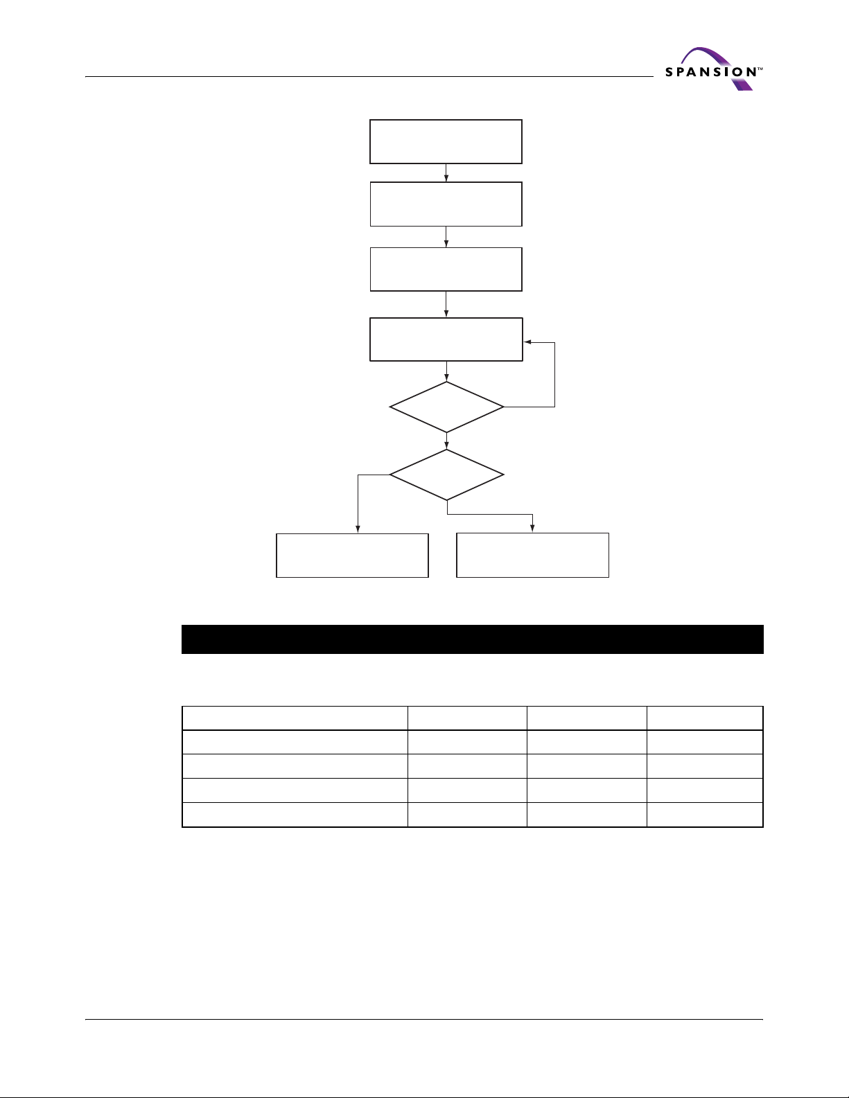
In single word programming mode, four Flash command write cycles are used to program an individual Flash address. While this method is supported by all Spansion devices, in general it is not
recommended for devices that support Write Buffer Programming. See
quired bus cycles and Figure 7.1 for the flowchart.
When the Embedded Program algorithm is complete, the device then returns to the read mode
and addresses are no longer latched. The system can determine the status of the program oper
ation by using DQ7 or DQ6. See Write Operation Status for information on these status bits.
Single word programming is supported for backward compatibility with existing Flash driver software and use of write buffer programming is strongly recommended for general programming.
The effective word programming time using write buffer programming is appro ximately four times
faster than the single word programming time.
Table 12.1 for the re-
-
26 S29PL-N MirrorBit™ Flash Family S29PL-N_00_A4 November 23, 2005
Page 29
Preliminary
Write Unlock Cycles:
Address 555h, Data AAh
Address 2AAh, Data 55h
Write Program Command:
Address 555h, Data A0h
Program Data to Address:
Yes
PA, PD
Perform Polling Algorithm
(see Write Operation Status
flowchart)
Polling Status
= Busy?
No
Polling Status
= Done?
No
Unlock Cycle 1
Unlock Cycle 2
Setup Command
Program Address (PA),
Program Data (PD)
Yes
Error condition
(Exceeded Timing Limits)
PASS. Device is in
read mode.
FAIL. Issue reset command
to return to read array mode.
Figure 7.1 Single Word Program Operation
Software Functions and Sample Code
Ta b l e 7 .7 S i ng le Wo r d P ro g r a m
(LLD Function = lld_ProgramCmd)
Cycle Operation Word Address Data
Unlock Cycle 1 Write Base + 555h 00AAh
Unlock Cycle 2 Write Base + 2AAh 0055h
Program Setup Write Base + 555h 00A0h
Program Write Word Address Data Word
Note: Base = Base Address.
The following is a C source code example of using the single word program function. See the
Spansion Low Level Driver User’s Guide (available on www.amd.com and www.fujitsu.com)
for general information on Spansion Flash memory software development guidelines.
/* Example: Program Command */
*((UINT16 *)base_addr + 0x555) = 0x00AA; /* write unlock cycle 1 */
*((UINT16 *)base_addr + 0x2AA) = 0x0055; /* write unlock cycle 2 */
*((UINT16 *)base_addr + 0x555) = 0x00A0; /* write program setup command */
*((UINT16 *)pa) = data; /* write data to be programmed */
/* Poll for program completion */
November 23, 2005 S29PL-N_00_A4 S29PL-N MirrorBit™ Flash Family 27
Page 30

7.4.2 Write Buffer Programming
Write Buffer Programming allows the system to write a maximum of 32 words in one programming operation. This results in a faster effective word programming time than the standard word
programming algorithms. The Write Buffer Programming command sequence is initiated by first
writing two unlock cycles. This is followed by a third write cycle containing the Write Buffer Load
command written at the Sector Address in which programming occurs. At this point, the system
writes the number of word locations minus 1 that is loaded into the page buffer at the Sector Ad
dress in which programming occurs. This tells the device how many write buffer addresses are
loaded with data and therefore when to expect the Program Buffer to Flash confirm command.
The number of locations to program cannot exceed the size of the write buffer or the operation
aborts. (Number loaded = the number of locations to program minus 1. For example, if the sys
tem programs 6 address locations, then 05h should be written to the device.)
The system then writes the starting address/data combination. This starting address is the first
address/data pair to be programmed, and selects the write-buffer-p age address. All subsequent
address/data pairs must fall within the elected-write-buffer-page.
The write-buffer-page is selected by using the addresses A
The write-buffer-page addresses must be the same for all address/data pairs loaded into the write
buffer. (This means Write Buffer Programming cannot be performed across multiple write-buffer-
page. This also means that Write Buffer Programming cannot be performed across multiple sec
tors. If the system attempts to load progra mming data outside of the selected write-buffer-page,
the operation
After writing the Starting Address/Data pair, the system then writes the remaining address/data
pairs into the write buffer.
Note that if a Write Buffer address location is loaded multiple times, the address/data pair counter
decrements for every data load operation. Also, the last data loaded at a location before the Pro
gram Buffer to Flash confirm command is programmed into the device. The software takes care
of the ramifications of loading a write-buffer location more than once. The counter decrements
for each data load operation,
fied number of write buffer locations have been loaded, the system must then write the Program
Buffer to Flash command at the Sector Address. Any other address/data write combinations abort
the Write Buffer Programming operation. The device then goes busy. The Data Bar polling tech
niques should be used while monitoring the last address location loaded into the write buffer . This
eliminates the need to store an address in memory because the system can load the last address
location, issue the program confirm command at the last loaded address location, and then data
bar poll at that same address.
The write-buffer embedded programming operation can be suspended using the standard suspend/resume commands. Upon successful completion of the Wr ite Buffer Programming operat ion,
the device returns to READ mode.
If the write buffer command sequence is entered incorrectly the device enters write buffer abort .
When an abort occurs the write-to buffer-abort reset command must be issued to return the de
vice to read mode.
The Write Buffer Programming Sequence is ABORTED under any of the following conditions:
Load a value that is greater than the page buffer size during the Number of Locations to Pro-
gram step.
Write to an address in a sector different than the one specified during the Write-Buffer-Load
command.
Write an Address/Data pair to a different write-buffer-page than the one selected by the
Starting Address during the write buffer data loading stage of the operation.
Write data other than the Confirm Command after the specified number of data load cycles.
ABORTS.)
NOT for each unique write-buffer-address location. Once the speci-
Preliminary
max
-
-
– A5.
-
-
-
-
28 S29PL-N MirrorBit™ Flash Family S29PL-N_00_A4 November 23, 2005
Page 31
Preliminary
Use of the write buffer is strongly recommended for programming when multiple words are to be
programmed. Write buffer programming is approximately four times faster than programming
one word at a time. Note that the Secured Silicon, the CFI functions, and the Autoselect Codes
are not available for read when a write buffer programming operation is in progress.
Software Functions and Sample Code
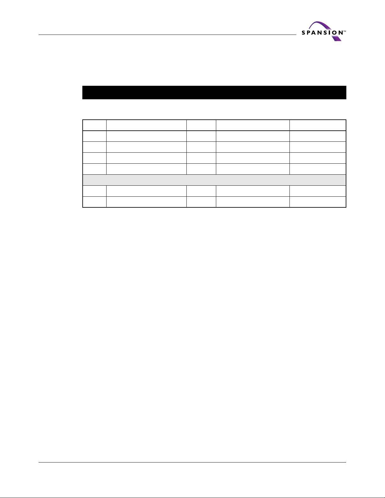
Table 7.8 Write Buffer Program
(LLD Functions Used = lld_WriteToBufferCmd, lld_ProgramBufferToFlashCmd)
Cycle Description Operation Word Address Data
1 Unlock Write Base + 555h 00AAh
2 Unlock Write Base + 2AAh 0055h
3 Write Buffer Load Command Write Program Address 0025h
4 Write Word Count Write Program Address Word Count (N–1)h
Number of words (N) loaded into the write buffer can be from 1 to 32 words.
5 to 36 Load Buffer Word N Write Program Address, Word N Word N
Last Write Buffer to Flash Write Sector Address 0029h
Notes:
1. Base = Base Address.
2. Last = Last cycle of write buffer program operation; depending on number of words written, the total number of cycles
can be from 6 to 37.
3. For maximum efficiency, it is recommended tha t the write buffer be loaded with the highest number of words (N words)
possible.
The following is a C source code example of using the write buffer program function. See the
Spansion Low Level Driver User’s Guide (available on www.amd.com and www.fujitsu.com)
for general information on Spansion Flash memory software development guidelines.
/* Example: Write Buffer Programming Command */
/* NOTES: Write buffer programming limited to 16 words. */
/* All addresses to be written to the flash in */
/* one operation must be within the same flash */
/* page. A flash page begins at addresses */
/* evenly divisible by 0x20. */
UINT16 *src = source_of_data; /* address of source data */
UINT16 *dst = destination_of_data; /* flash destination address */
UINT16 wc = words_to_program -1; /* word count (minus 1) */
*((UINT16 *)base_addr + 0x555) = 0x00AA; /* write unlock cycle 1 */
*((UINT16 *)base_addr + 0x2AA) = 0x0055; /* write unlock cycle 2 */
*((UINT16 *)sector_address) = 0x0025; /* write write buffer load command */
*((UINT16 *)sector_address) = wc; /* write word count (minus 1) */
loop:
*dst = *src; /* ALL dst MUST BE SAME PAGE */ /* write source data to destination */
dst++; /* increment destination pointer */
src++; /* increment source pointer */
if (wc == 0) goto confirm /* done when word count equals zero */
wc--; /* decrement word count */
goto loop; /* do it again */
confirm:
*((UINT16 *)sector_address) = 0x0029; /* write confirm command */
/* poll for completion */
/* Example: Write Buffer Abort Reset */
*((UINT16 *)addr + 0x555) = 0x00AA; /* write unlock cycle 1 */
*((UINT16 *)addr + 0x2AA) = 0x0055; /* write unlock cycle 2 */
*((UINT16 *)addr + 0x555) = 0x00F0; /* write buffer abort reset */
November 23, 2005 S29PL-N_00_A4 S29PL-N MirrorBit™ Flash Family 29
Page 32

Preliminary
Write Next Word,
Decrement wc:
PA data , wc = wc – 1
No
Write Unlock Cycles:
Address 555h, Data AAh
Address 2AAh, Data 55h
Write Buffer Load Command:
Address 555h, Data 25h
Load Word Count to Program
Program Data to Address:
Sector Address to Cause
Issue
SA = wc
wc = 0?
No
Write Buffer
Abort Desired?
Yes
Write to a Different
Write Buffer Abort
Yes
Unlock Cycle 1
Unlock Cycle 2
wc = number of words – 1
Confirm command:
SA 29h
Wait 4 µs
Perform Polling Algorithm
(see Write Operation Status
flowchart)
Polling Status
= Done?
Yes
RESET. Issue Write Buffer
Abort Reset Command
7.4.3 Sector Erase
The sector erase function erases one or more sectors in the memory array. (See Table 12.1, and
Figure 7.3.) The device does not require the system to preprogram prior to erase. The Embedded
Erase algorithm automatically programs and verifies the entire memory for an all zero data pattern prior to electrical erase. The system is not required to pro vide any controls or timings during
these operations.
After the command sequence is written, a sector erase time-out of no less than t
ing the time-out period, additional sector addresses and sector erase commands can be written.
Loading the sector erase buffer can be done in any sequence, and the number of sectors can be
from one sector to all sectors. The time between these additional cycles must be less than t
Any sector erase address and command following the exceeded time-out (t
No
Yes
Write Buffer
Abort?
No
FAIL. Issue reset command
to return to read array mode.
Figure 7.2 Write Buffer Programming Operation
No
Error?
Yes
PASS. Device is in
read mode.
occurs. Dur-
SEA
) may or may not
SEA
SEA
.
30 S29PL-N MirrorBit™ Flash Family S29PL-N_00_A4 November 23, 2005
Page 33
Preliminary
be accepted. Any command other than Sector Er ase or Erase Suspend during the time-out period
resets that bank to the read mode. The system can monito r DQ3 to deter mine if the sector er ase
timer has timed out (
see DQ3: Sector Erase Timeout State Indicator ). The time-out begins from
the rising edge of the final WE# pulse in the command sequence.
When the Embedded Erase algorithm is complete, the bank returns to read ing array data and ad-
dresses are no longer latched. Note that while the Embedded Erase operation is in progress, the
system can read data from the non-erasing banks. The system can determine the status of the
erase operation by reading DQ7 or DQ6/DQ2 in the er asing bank.
See Write Operation Status for
information on these status bits.
Once the sector erase operation has begun, only the Erase Suspend command is valid. All other
commands are ignored. However, note that a hardware reset immediately terminates the erase
operation. If that occurs, the sector erase command sequence should be reinitiated once that
bank has returned to reading array data, to ensure data integrity.
Figure 7.3 illustrates the algorithm for the erase operation. See AC Characteristics for the Erase/
Program Operations para met ers and timing diag rams.
Software Functions and Sample Code
Ta b l e 7 .9 Se ct o r E ra se
(LLD Function = lld_SectorEraseCmd)
Cycle Description Operation Word Address Data
1 Unlock Write Base + 555h 00AAh
2 Unlock Write Base + 2AAh 0055h
3 Setup Command Write Base + 555h 0080h
4 Unlock Write Base + 555h 00AAh
5 Unlock Write Base + 2AAh 0055h
6 Sector Erase Command Write Sector Address 0030h
Unlimited additional sectors can be selected for erase; command(s) must be written within t
SEA
The following is a C source code example of using the sector erase function. Refer to the
Spansion Low Level Driver User’s Guide (available on www.amd.com and www.fujitsu.com)
for general information on Spansion Flash memory software development guidelines.
/* Example: Sector Erase Command */
*((UINT16 *)base_addr + 0x555) = 0x00AA; /* write unlock cycle 1 */
*((UINT16 *)base_addr + 0x2AA) = 0x0055; /* write unlock cycle 2 */
*((UINT16 *)base_addr + 0x555) = 0x0080; /* write setup command */
*((UINT16 *)base_addr + 0x555) = 0x00AA; /* write additional unlock cycle 1 */
*((UINT16 *)base_addr + 0x2AA) = 0x0055; /* write additional unlock cycle 2 */
*((UINT16 *)sector_address) = 0x0030; /* write sector erase command */
.
November 23, 2005 S29PL-N_00_A4 S29PL-N MirrorBit™ Flash Family 31
Page 34
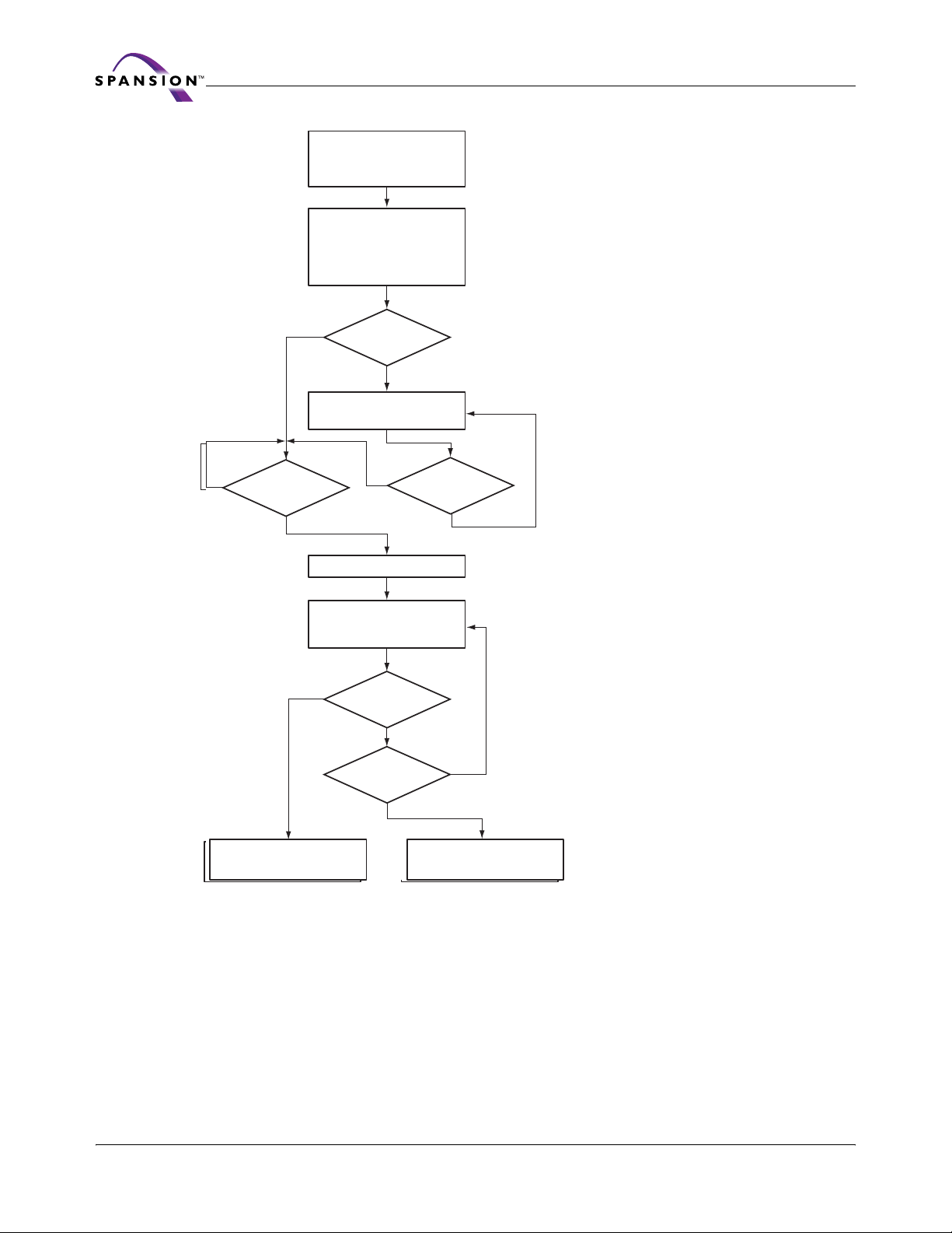
No
No
Poll DQ3.
Poll DQ3.
DQ3 = 1?
DQ3 = 1?
Yes
Yes
Write Unlock Cycles:
Write Unlock Cycles:
Address 555h, Data AAh
Address 555h, Data AAh
Address 2AAh, Data 55h
Address 2AAh, Data 55h
Write Sector Erase Cycles:
Write Sector Erase Cycles:
Address 555h, Data 80h
Address 555h, Data 80h
Address 555h, Data AAh
Address 555h, Data AAh
Address 2AAh, Data 55h
Address 2AAh, Data 55h
Sector Address, Data 30h
Sector Address, Data 30h
Select
No
No
Select
Additional
Additional
Sectors?
Sectors?
Yes
Yes
Write Additional
Write Additional
Sector Addresses
Sector Addresses
Yes
Yes
Preliminary
Last Sector
Last Sector
Selected?
Selected?
No
No
Unlock Cycle 1
Unlock Cycle 1
Unlock Cycle 2
Unlock Cycle 2
Command Cycle 1
Command Cycle 1
Command Cycle 2
Command Cycle 2
Command Cycle 3
Command Cycle 3
Specify first sector for erasure
Specify first sector for erasure
• Each additional cycle must be written within t
• Each additional cycle must be written within t
• Timeout resets after each additional cycle is written
• Timeout resets after each additional cycle is written
• The host system may monitor DQ3 or wait t
• The host system may monitor DQ3 or wait t
acceptance of erase commands
acceptance of erase commands
• No limit on number of sectors
• No limit on number of sectors
• Commands other than Erase Suspend or selecting
• Commands other than Erase Suspend or selecting
additional sectors for erasure during timeout reset device
additional sectors for erasure during timeout reset device
to reading array data
to reading array data
timeout
SEA
SEA
to ensure
to ensure
SEA
SEA
timeout
Wait 4 µs
Wait 4 µs
Perform Write Operation
Perform Write Operation
Status Algorithm
Status Algorithm
Yes
Yes
PASS. Device returns
PASS. Device returns
to reading array.
to reading array.
Done?
Done?
No
No
DQ5 = 1?
DQ5 = 1?
Yes
Yes
No
No
FAIL. Write reset command
FAIL. Write reset command
to return to reading array.
to return to reading array.
Notes:
1. See Table 12.1 for erase command sequence.
2. See the section on DQ3 for information on the sector erase timeout.
Figure 7.3 Sector Erase Operation
7.4.4 Chip Erase Command Sequence
Chip erase is a six-bus cycle operation as indicated by Table 12.1. These commands invoke the
Embedded Erase algorithm, which does not require the system to preprogr am prior to er ase. The
Embedded Erase algorithm automatically preprograms and verifies the entire memory for an all
zero data pattern prior to electrical erase. The system is not required to provide any controls or
timings during these operations. The Command Definition tables (
show the address and data requirements for the chip erase command sequence.
Status may be obtained by reading DQ7, DQ6 and/or DQ2.
Status may be obtained by reading DQ7, DQ6 and/or DQ2.
Error condition (Exceeded Timing Limits)
Error condition (Exceeded Timing Limits)
Table 12.1 and Table 12.2)
32 S29PL-N MirrorBit™ Flash Family S29PL-N_00_A4 November 23, 2005
Page 35
Preliminary
When the Embedded Erase algorithm is complete, that bank returns to the read mode and addresses are no longer latched. The system can determine the status of the erase operation by
using DQ7 or DQ6/DQ2. See
Write Operation Status for information on these status bits.
Any commands written during the chip erase operation are ignored. However, note that a hardware reset immediately terminates the erase operation. If that occurs, the chip erase command
sequence should be reinitiated once that bank has returned to reading array data, to ensure data
integrity.
Software Functions and Sample Code
Table 7.10 Chip Erase
(LLD Function = lld_ChipEraseCmd)
Cycle Description Operation Word Address Data
1 Unlock Write Base + 555h 00AAh
2 Unlock Write Base + 2AAh 0055h
3
Setup
Command
Write Base + 555h 0080h
4 Unlock Write Base + 555h 00AAh
5 Unlock Write Base + 2AAh 0055h
6
Chip Erase
Command
Write Base + 555h 0010h
The following is a C source code example of using the chip erase function. Refer to the Span-
sion Low Level Driver User’s Guide (available on www.amd.com and www.fujitsu.com) for
general information on Spansion Flash memory software development guidelines.
/* Example: Chip Erase Command */
/* Note: Cannot be suspended */
*((UINT16 *)base_addr + 0x555) = 0x00AA; /* write unlock cycle 1 */
*((UINT16 *)base_addr + 0x2AA) = 0x0055; /* write unlock cycle 2 */
*((UINT16 *)base_addr + 0x555) = 0x0080; /* write setup command */
*((UINT16 *)base_addr + 0x555) = 0x00AA; /* write additional unlock cycle 1 */
*((UINT16 *)base_addr + 0x2AA) = 0x0055; /* write additional unlock cycle 2 */
*((UINT16 *)base_addr + 0x000) = 0x0010; /* write chip erase command */
7.4.5 Erase Suspend/Erase Resume Commands
The Erase Suspend command allows the system to interrupt a sector erase operation and then
read data from, or program data to, any sector not select ed for er asure. The bank address is re
quired when writing this command. This command is valid only during the sector erase operation,
including the minimum t
Erase Suspend command is ignored if written during the chip erase operation.
When the Erase Suspend command is written during the sector erase operation, the device requires a maximum of t
when the Erase Suspend command is written during the sector erase time-out, the device imme
diately terminates the time-out period and suspends the erase operation.
After the erase operation has been suspended, the bank enters the erase-suspend-read mode.
The system can read data from or program data to any sector not selected for er asure . (The d e
vice erase s uspends all sectors selected for erasure.) Reading at any address within erasesuspended sectors produces status information on DQ7-DQ0. The system can use DQ7, or DQ6,
and DQ2 together, to determine if a sector is actively erasing or is erase-suspended. Refer to
Table 7.18 for information on these status bits.
time-out period during the sector erase command sequence. The
SEA
(erase suspend latency) to suspend the erase operation. However,
ESL
-
-
-
November 23, 2005 S29PL-N_00_A4 S29PL-N MirrorBit™ Flash Family 33
Page 36
Preliminary
After an erase-suspended program operation is complete, t he bank returns to the erase-suspendread mode. The system can determine the status of the program operation using the DQ7 or DQ6
status bits, just as in the standard program operation.
In the erase-suspend-read mode, the system can also issue the Autoselect command sequence.
See Write Buffer Programming and Autoselect for details.
To resume the sector erase operation, the system must write the Erase Resume command. The
bank address of the erase-suspended bank is required when writing this command. Further writes
of the Resume command are ignored. Another Erase Suspend command can be written after the
chip has resumed erasing.
Software Functions and Sample Code
Table 7.11 Erase Suspend
(LLD Function = lld_EraseSuspendCmd)
Cycle Operation Word Address Data
1 Write Bank Address 00B0h
The following is a C source code example of using the erase suspend function. Refer to the
Spansion Low Level Driver User’s Guide (available on www.amd.com and www.fujitsu.com)
for general information on Spansion Flash memory software development guidelines.
/* Example: Erase suspend command */
*((UINT16 *)bank_addr + 0x000) = 0x00B0; /* write suspend command */
Ta b l e 7 .1 2 E ra s e R es um e
(LLD Function = lld_EraseResumeCmd)
Cycle Operation Word Address Data
1 Write Bank Address 0030h
The following is a C source code example of using the erase resume function. Refer to the
Spansion Low Level Driver User’s Guide (available on www.amd.com and www.fujitsu.com)
for general information on Spansion Flash memory software development guidelines.
/* Example: Erase resume command */
*((UINT16 *)bank_addr + 0x000) = 0x0030; /* write resume command */
/* The flash needs adequate time in the resume state */
7.4.6 Program Suspend/Program Resume Commands
The Program Suspend command allows the system to interrupt an embedded programming operation or a Write to Buffer programming operation so that data can read from any non-
suspended sector. When the Program Suspend command is written during a programmin g pro
cess, the device halts the programming operation within t
updates the status bits.
After the programming operation has been suspende d, the syste m can read arr ay data from an y
non-suspended sector. The Program Suspend command can also be issued during a programming
operation while an erase is suspended. In this case, data can be read from any addresses not in
Erase Suspend or Program Suspend. If a read is needed from the Secured Silicon Sector area,
then user must use the proper command sequences to enter and exit this region.
(program suspend latency) and
PSL
-
34 S29PL-N MirrorBit™ Flash Family S29PL-N_00_A4 November 23, 2005
Page 37
Preliminary
The system can also write the Autoselect command sequence when the device is in Program Suspend mode. The device allows reading Autoselect codes in the suspended sectors, since the codes
are not stored in the memory array. When the device exits the Autoselect mode, the device re
verts to Program Suspend mode, and is ready for another valid operation. See Autoselect for
more information.
After the Program Resume command is written, the device reverts to programming. The system
can determine the status of the program operation using the DQ7 or DQ6 status bits, just as in
the standard program operation. See
Write Operation Status for more info r mat i on .
The system must write the Program Resume command (address bits are don't cares) to exit the
Program Suspend mode and continue the programming opera tion. Further w rites of the Progr am
Resume command are ignored. Another Progr am Suspend command can be written after the de
vice has resumed programming.
Software Functions and Sample Code
Table 7.13 Program Suspend
(LLD Function = lld_ProgramSuspendCmd)
Cycle Operation Word Address Data
1 Write Bank Address 00B0h
-
-
The following is a C source code example of using the program suspend function. Refer to the
Spansion Low Level Driver User’s Guide (available on www.amd.com and www.fujitsu.com)
for general information on Spansion Flash memory software development guidelines.
/* Example: Program suspend command */
*((UINT16 *)base_addr + 0x000) = 0x00B0; /* write suspend command */
Cycle Operation Word Address Data
1 Write Bank Address 0030h
The following is a C source code example of using the program resume function. Refer to the
Spansion Low Level Driver User’s Guide (available on www.amd.com and www.fujitsu.com)
for general information on Spansion Flash memory software development guidelines.
/* Example: Program resume command */
*((UINT16 *)base_addr + 0x000) = 0x0030; /* write resume command */
7.4.7 Accelerated Program
Accelerated single word programming, write buffer programming, sector erase, and chip erase
operations are enabled through the ACC function. This method is faster than the standard chip
program and erase command sequences.
The accelerated chip program and erase functions must not be used more than 10
times per sector. In addition, accelerated chip program and era se should be performed at room
temperature (25
This function is primarily intended to allow faster manufacturing throughput at the factory . If the
system asserts V
pass mode and uses the higher voltage on the input to reduce the time required for progr am and
erase operations. The system can then use the Write Buffer Load command sequence provided
by the Unlock Bypass mode. Note that if a Write-to-Buffer-Abort Reset is required while in Unlock
°C ±10°C).
on this input, the device automatically enters the aforementioned Unlock By-
HH
Ta b l e 7 .1 4 P ro gr a m R es um e
(LLD Function = lld_ProgramResumeCmd)
November 23, 2005 S29PL-N_00_A4 S29PL-N MirrorBit™ Flash Family 35
Page 38
Bypass mode, the full 3-cycle RESET command sequence must be used to reset the device. Removing VHH from the ACC input, upon completion of the embedded program or erase operation,
returns the device to normal operation.
Sectors must be unlocked prior to raising WP#/ACC to VHH.
The WP#/ACC must not be at V
accelerated chip erase, or device damage can result.
Set the ACC pin at V
7.4.8 Unlock Bypass
The device features an Unlock Bypass mode to facilitate faster word programming. Once the device enters the Unlock Bypass mode, only two write cycles are required to program data, instead
of the normal four cycles.
This mode dispenses with the initial two unlock cycles required in the standard program command
sequence, resulting in faster total programming time.
shows the requirements for the unlock bypass command sequences.
During the unlock bypass mode, only the Read, Unlock Bypass Program and Unlock Bypass Reset
commands are valid. T o exit the unlock bypass mode, the system must issue the two-cycle unlock
bypass reset command sequence. The first cycle must contain the bank address and the data 90h.
The second cycle need only contain the data 00h. The bank then returns to the read mode.
Preliminary
for operations other than accelerated programming and
HH
when accelerated programming not in use.
CC
Table 12.1, Memory Array Commands
Software Functions and Sample Code
The following are C source code examples of using the unlock bypass entry, program, and exit
functions. Refer to the Spansion Low Level Driver User’s Guide (availabl e soon on www.amd.com
and www.fujitsu.com) for general information on Spansion Flash memory software development
guidelines.
Table 7.15 Unlock Bypass Entry
(LLD Function = lld_UnlockBypassEntryCmd)
Cycle Description Operation Word Address Data
1 Unlock Write Base + 555h 00AAh
2 Unlock Write Base + 2AAh 0055h
3 Entry Command Write Base + 555h 0020h
/* Example: Unlock Bypass Entry Command */
*((UINT16 *)bank_addr + 0x555) = 0x00AA; /* write unlock cycle 1 */
*((UINT16 *)bank_addr + 0x2AA) = 0x0055; /* write unlock cycle 2 */
*((UINT16 *)bank_addr + 0x555) = 0x0020; /* write unlock bypass command */
/* At this point, programming only takes two write cycles. */
/* Once you enter Unlock Bypass Mode, do a series of like */
/* operations (programming or sector erase) and then exit */
/* Unlock Bypass Mode before beginning a different type of */
/* operations. */
36 S29PL-N MirrorBit™ Flash Family S29PL-N_00_A4 November 23, 2005
Page 39
Preliminary
Cycle Description Operation Word Address Data
1 Program Setup Command Write Base +xxxh 00A0h
2 Program Command Write Program Address Program Data
/* Example: Unlock Bypass Program Command */
/* Do while in Unlock Bypass Entry Mode! */
*((UINT16 *)bank_addr + 0x555) = 0x00A0; /* write program setup command */
*((UINT16 *)pa) = data; /* write data to be programmed */
/* Poll until done or error. */
/* If done and more to program, */
/* do above two cycles again. */
Cycle Description Operation Word Address Data
1 Reset Cycle 1 Write Base +xxxh 0090h
2 Reset Cycle 2 Write Base +xxxh 0000h
/* Example: Unlock Bypass Exit Command */
*( (UINT16 *)base_addr + 0x000 ) = 0x0090;
*( (UINT16 *)base_addr + 0x000 ) = 0x0000;
7.4.9 Write Operation Status
The device provides several bits to determine the status of a program or erase operation. The
following subsections describe the function of DQ1, DQ2, DQ3, DQ5, DQ6, and DQ7.
DQ7: Data# Polling. The Data# Polling bit, DQ7, indicates to the host system whether an Em-
bedded Program or Erase algorithm is in progress or completed, or whether a bank is in Erase
Suspend. Data# Polling is valid after the rising edge of the final WE# pulse in the command se
quence. Note that the Data# Polling is v alid only for the last word being programmed in the writebuffer-page during Write Buffer Programming. Reading Data# Polling status on any word other
than the last word to be programmed in the write-buffer-page returns false status information.
During the Embedded Program algorithm, the device outputs on DQ7 the complement of the
datum programmed to DQ7. This DQ7 status also applies to programming during Erase Suspend.
When the Embedded Program algorithm is complete, the device outputs the datum progr ammed
to DQ7. The system must provide the program address to read valid status information on DQ7.
If a program address falls within a protected sector, Data# polling on DQ7 is active for approxi
mately t
During the Embedded Erase Algorithm, Data# polling produces a 0 on DQ7. When the Embedded
Erase algorithm is complete, or if the bank enters the Erase Suspend mode, Data# Polling pro
duces a 1 on DQ7. The system must provide an address within any of the sectors selected for
erasure to read valid status information on DQ7.
After an erase command sequence is written, if all sectors selected for erasing are protected,
Data# Polling on DQ7 is active for approximately t
If not all selected sectors are protected, the Embedded Erase algorithm erases the unprotected
sectors, and ignores the selected sectors that are protected. However, if the system reads DQ7
at an address within a protected sector, the status may not be valid.
Just prior to the completion of an Embedded Program or Erase operation, DQ7 can change asynchronously with DQ6 – DQ0 while Output Enable (OE#) is asserted low. That is, the device may
change from providing status information to valid data on DQ7. Depending on when the system
, then that bank returns to the read mode.
PSP
Table 7.16 Unlock Bypass Program
(LLD Function = lld_UnlockBypassProgramCmd)
Table 7.17 Unlock Bypass Reset
(LLD Function = lld_UnlockBypassResetCmd)
, then the bank returns to the read mode.
ASP
-
-
-
November 23, 2005 S29PL-N_00_A4 S29PL-N MirrorBit™ Flash Family 37
Page 40

Preliminary
samples the DQ7 output, it may read the status or valid data. Even if the device has completed
the program or erase operation and DQ7 ha s v alid data, the data out puts on DQ6
still invalid. Valid data on DQ7
See the following for more information: Table 7.18, Write Operation Status, shows the outputs
for Data# Polling on DQ7. Figure 7.4, Write Oper ation Stat us Flowchart , shows the Data# Polling
algorithm. Figure 11.13, Data# P olling Timings (During Embedded Algorithms) shows the Data#
Polling timing diagram.
– DQ0 appears on successive read cycles.
– DQ0 may be
38 S29PL-N MirrorBit™ Flash Family S29PL-N_00_A4 November 23, 2005
Page 41
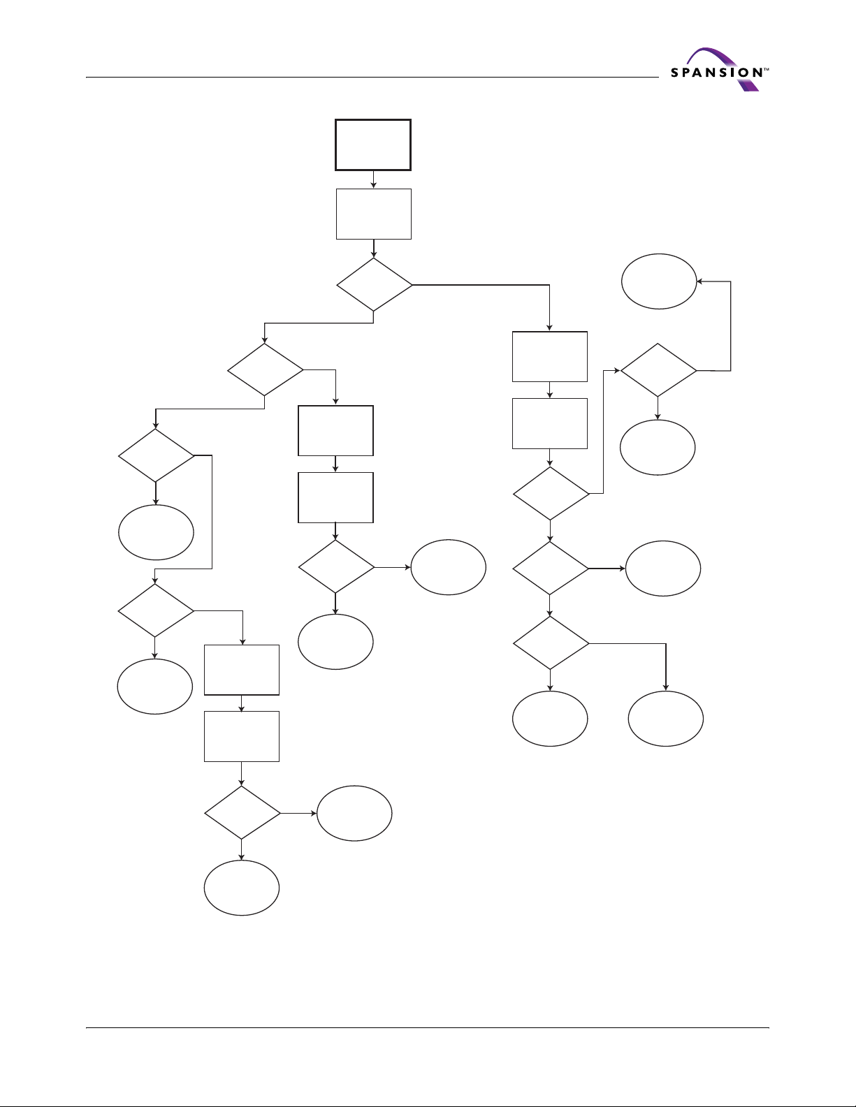
Preliminary
START
Read 1
(Note 4)
Write Buffer
Programming?
NO
Device BUSY,
Re-Poll
Read3
DQ1=1?
NO
Device BUSY,
Re-Poll
YES
YES
DQ5=1?
Read 2
Read 3
Read 1
YES
NO
(Note 1)
(Note 6)
DQ7=valid
Read 2
Read 3
DQ6
toggling?
NO
Device BUSY,
Re-Poll
data?
YES
YES
NO
(Note 3)
TIMEOUT
(Note 1)
(Note 2)
Read 2
Read 3
Programming
Operation?
NO
DQ6
toggling?
NO
DQ2
toggling?
NO
Erase
Operation
Complete
YES
YES
YES
Erase
Operation
Complete
YES
Read3=
valid data?
NO
Program
Operation
Failed
DEVICE
ERROR
Device in
Erase/Suspend
Mode
(Note 5)
Notes:
Read3
DQ1=1
AND DQ7 ≠
Valid Data?
NO
Device BUSY,
Re-Poll
YES
Write Buffer
Operation
Failed
1. DQ6 is toggling if Read2 DQ6 does not equal Read3 DQ6.
2. DQ2 is toggling if Read2 DQ2 does not equal Read3 DQ2.
3. May be due to an attempt to program a 0 to 1. Use the RESET
command to exit operation.
4. Write buffer error if DQ1 of last read =1.
5. Invalid state, use RESET command to exit operation.
6. Valid data is the data that is intended to be programmed or all 1's for
an erase operation.
7. Data polling algorithm valid for all operations except advanced sector
protection.
Figure 7.4 Write Operation Status Flowchart
November 23, 2005 S29PL-N_00_A4 S29PL-N MirrorBit™ Flash Family 39
Page 42

Preliminary
DQ6: Toggle Bit I . Toggle Bit I on DQ6 indicates whether an Embedded Program or Erase algo-
rithm is in progress or complete, or whether the device has entered the Erase Suspend mode.
Toggle Bit I can be read at any address in the same bank, and is valid after the rising edge of the
final WE# pulse in the command sequence (prior to the program or erase operation), and during
the sector erase time-out.
During an Embedded Program or Erase algorithm operation, successive read cycles to any address cause DQ6 to toggle. When the operation is complete, DQ6 stops toggling.
After an erase command sequence is written, if all sectors selected for erasing are protected, DQ6
toggles for approximately t
data. If not all selected sectors are protected, the Embedded Erase algorithm erases the unpro
tected sectors, and ignores the selected sectors that are protected.
The system can use DQ6 and DQ2 together to determine whether a sector is actively erasing or
is erase-suspended. When the device is actively erasing (that is, the Embedded Erase algorithm
is in progress), DQ6 toggles. When the device enters the Erase Suspend mode, DQ6 stops tog
gling. However, the system must also use DQ2 to determine which sectors are erasing or erasesuspended. Alternatively, the system can use DQ7,
If a program address falls within a protected sector, DQ6 toggles for approximately t
program command sequence is written, then returns to reading array data.
DQ6 also toggles during the erase-suspend-program mode, and stops t oggling once the Embedded Program Algorithm is complete.
See the following for additional information: Figure 7.4, Write Operation Status Flowchart,
Figure 11.14, Toggle Bit Timings (During Embed ded Algorithms), Table 7.18, Write Operation
Status, and Figure 11.15, DQ2 vs. DQ6.
Toggl e Bit I on DQ6 requires eithe r OE# or CE# to be de-assert ed and reasserted to show th e
change in state.
DQ2: Toggle Bit II . The Toggle Bit II on DQ2, when used with DQ6, indicates whether a partic-
ular sector is actively erasing (that is, the Embedded Erase algorithm is in progress), or whether
that sector is erase-suspended. Toggle Bit II is valid after the rising edge of the final WE# pulse
in the command sequence. DQ2 toggles when the system reads at addresses within those sectors
that have been selected for erasure. But DQ2 cannot distinguish whether the sector is actively
erasing or is erase-suspended. DQ6, by comparison, indicates whether the device is actively eras
ing, or is in Erase Suspend, but cannot distinguish which sectors are selected for erasure. Thus,
both status bits are required for sector and mode information. Refer to
tion Status to compare outputs for DQ2 and DQ6. See the following for additional information:
Figure 7.4, Write Operation Status Flowchart and Figure 11.14, Toggle Bit Timings (During Em-
bedded Algorithms).
Reading Toggle Bits DQ6/DQ2. Whenever the system initially begins reading toggle bit status,
it must read DQ7
– DQ0 at least twice in a row to determine whether a toggle bit is toggling. Typically, the system would note and store the value of the toggle bit after the first read. After the
second read, the system would compare the new value of the toggle bit wit h the first. If the toggle
bit is not toggling, the device has completed the program or erases operation. The system can
read array data on DQ7
cycles, the system determines that the toggle bit is still toggling, the system also should note
whether the value of DQ5 is high (see the section on DQ5). If it is, the system should then deter
mine again whether the toggle bit is toggling, since the toggle bit might have stopped toggling
just as DQ5 went high. If the toggle bit is no longer toggling, the device has successfully com
pleted the program or erases operation. If it is still toggling, the device did not complete the
operation successfully, and the system must write the reset command to return to reading array
data. The remaining scenario is that the system initially determines that the toggle bit is toggling
and DQ5 has not gone high. The system may continue to monitor the toggle bit and DQ5 through
(all sectors protected toggle time), then returns to reading array
ASP
see DQ7: Data# Polling.
after the
PAP
Table 7.18, Write Opera-
– DQ0 on the following read cycle. However, if after the initial two read
-
-
-
-
-
40 S29PL-N MirrorBit™ Flash Family S29PL-N_00_A4 November 23, 2005
Page 43

Preliminary
successive read cycles, determining the status as described in the previous paragraph. Alternatively, it can choose to perform oth er system tasks. In this case, the system must start at the
beginning of the algorithm when it returns to determine the sta tus of the operation. Refer to
Figure 7.4, Write Operation Status Flowchart for more details.
DQ5: Exceeded Timing Limits. DQ5 indicates whether the program or erase time has exceeded
a specified internal pulse count limit. Under these conditions DQ5 produces a 1, indicating that
the program or erase cycle was not successfully completed. The device may output a 1 on DQ5 if
the system tries to program a 1 to a location that was previously programmed to 0. Only an erase
operation can change a 0 back to a 1, Under this condition, the device halts the operation, and
when the timing limit has been exceeded, DQ5 produces a 1. Under both these conditions, the
system must write the reset command to return to the read mode (or to the erase-suspend-read
mode if a bank was previously in the erase-suspend-program mode).
DQ3: Sector Erase Timeout State Indicator. After writing a sector erase command sequence,
the system may read DQ3 to determine whether or not erasure has begun. (The sector erase
timer does not apply to the chip erase command.) If additional sectors are selected for erasure,
the entire time-out also applies after each additional sector erase command. When the time-out
period is complete, DQ3 switches from a 0 to a 1. If the time between additional sector erase
commands from the system can be assumed to be less than t
DQ3. See Sector Erase Command Sequence for more details.
After the sector erase command is written, the system should read the status of DQ7 (Data# Polling) or DQ6 (Toggle Bit I) to ensure that the device has accepted the command sequence, and
then read DQ3. If DQ3 is 1, the Embedded Erase algorithm has begun; all further commands (ex
cept Erase Suspend) are ignored until the erase operation is complete. If DQ3 is 0, the device
accepts additional sector erase commands. To ensure the command has been accepted, the sys
tem software should check the status of DQ3 prior to and following each sub-sequent sector erase
command. If DQ3 is high on the second status check, the last command might not have been
accepted.
DQ1: Write to Buffer Abort. DQ1 indicates whether a Write to Buffer operation was aborted.
Table 7.18 shows the status of DQ3 relative to the other status bits.
Under these conditions DQ1 produces a 1. The system must issue the Write to Buffer Abort Reset
command sequence to return the device to reading array data. See Write Buffer Programming
Operation for more details.
, the system need not monitor
SEA
-
-
November 23, 2005 S29PL-N_00_A4 S29PL-N MirrorBit™ Flash Family 41
Page 44
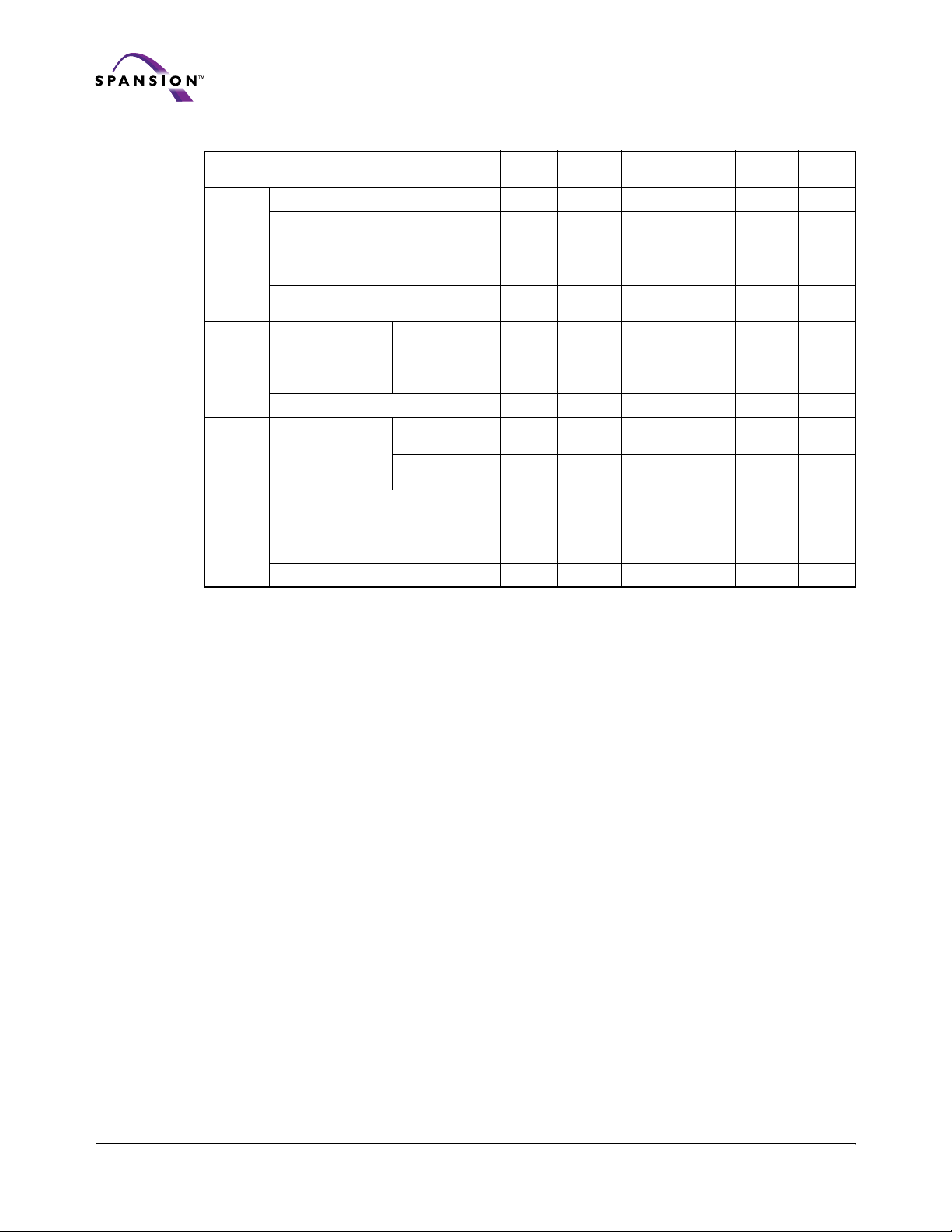
Preliminary
Table 7.18 Write Operation Status
Standard
Mode
Program
Suspend
Mode
(Note 3)
Erase
Suspend
Mode
Erase
Suspend
Mode
Write to
Buffer
(Note 5)
Status
Embedded Program Algorithm DQ7# Toggle 0 N/A No toggle 0
Embedded Erase Algorithm 0 Toggle 0 1 Toggle N/A
Reading within Program
Suspended Sector
Reading within Non-Program
Suspended Sector
Erase Suspended
Erase-Suspend-Read
Erase-Suspend-Program DQ7# Toggle 0 N/A N/A N/A
Erase-SuspendRead
Erase-Suspend-Program DQ7# Toggle 0 N/A N/A N/A
BUSY State DQ7# Toggle 0 N/A N/A 0
Exceeded Timing Limits DQ7# Toggle 1 N/A N/A 0
ABORT State DQ7# Toggle 0 N/A N/A 1
Sector
Non-Erase
Suspended Sector
Erase
Suspended Sector
Non-Erase
Suspended Sector
DQ7
(Note 2)
INVALID
(Not
Allowed)
Data Data Data Data Data Data
1 No Toggle 0 N/A Toggle N/A
Data Data Data Data Data Data
1 No toggle 0 N/A Toggle N/A
Data Data Data Data Data Data
DQ6
INVALID
(Not
Allowed)
DQ5
(Note 1)
INVALID
(Not
Allowed)
DQ3
INVALID
(Not
Allowed)
DQ2
(Note 2)
INVALID
(Not
Allowed)
DQ1
(Note 4)
INVALID
(Not
Allowed)
Notes:
1. DQ5 switches to ‘1’ when an Embedded Program or Embedded Erase operation has exceeded the maximum timing limits.
Refer to the section on DQ5 for more information.
2. DQ7 a valid address when reading status information. Refer to the appropriate subsection for further details.
3. Data are invalid for addresses in a Program Suspended sector.
4. DQ1 indicates the Write to Buffer ABORT status during Write Buffer Programming operations.
5. The data-bar polling algorithm should be used for Write Buffer Programming operations. Note that DQ7# during Write
Buffer Programming indicates the data-bar for DQ7 data for the LAST LOADED WRITE-BUFFER ADDRESS location.
42 S29PL-N MirrorBit™ Flash Family S29PL-N_00_A4 November 23, 2005
Page 45
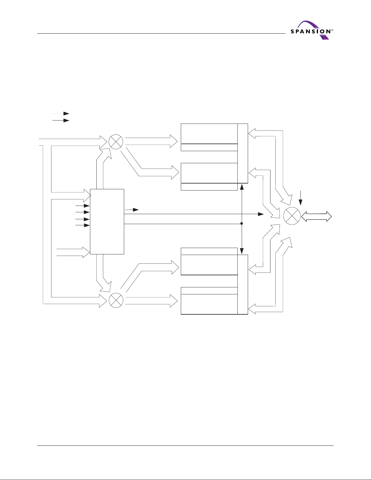
Preliminary
7.5 Simultaneous Read/Write
The simultaneous read/write feature allows the host system to read data from one bank of memory while programming or erasing another bank of memory. An erase operation may also be
suspended to read from or program another location within the same bank (except the sector
being erased).
cycles may be initiated for simultaneous operation with zero latency. See the table, DC Charac-
teristics for read-while-program and read-while-erase current specifications.
V
CC
V
SS
Figure 11.12, Back-to-back Read/Write Cycle Timings shows how read and write
Note: A
A
– A0
max
– A0A
max
A
A
–A0
max
RESET#
WE#
CE#
WP#/ACC
State
Control
and
Command
Register
DQ0 – DQ15
–A0
max
– A0
A
max
= A23 (PL256N), A22 (PL127N)
max
Mux
Mux
Bank A Address
Bank B Address
RY/BY#
Bank C Address
Bank D Address
Status
Control
Bank A
X-Decoder
Bank B
X-Decoder
X-Decoder
Bank C
X-Decoder
Bank D
Y-gate
Y-gate
DQ15–DQ0
OE#
DQ15–DQ0
DQ15 – DQ0
Mux
DQ15–DQ0
DQ15–DQ0
Figure 7.5 Simultaneous Operation Block Diagram for S29PL256N and S29PL127N
November 23, 2005 S29PL-N_00_A4 S29PL-N MirrorBit™ Flash Family 43
Page 46
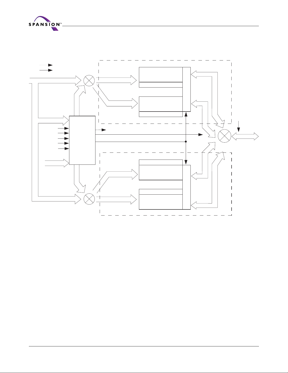
Preliminary
V
V
CC
SS
A21 – A0
A21 – A0
RESET#
WE#
CE1#
CE2#
WP#/ACC
DQ0 – DQ15
A21 – A0
Mux
A21 – A0A21 – A0
State
Control
and
Command
Register
Mux
CE1# = L
CE2# = H
Bank 1A Address
Bank 1B Address
RY/BY#
CE1# = H
CE2# = L
Bank 2A Address
Bank 2B Address
Status
Control
Bank 1A
X-Decoder
Bank 1B
X-Decoder
X-Decoder
Bank 2A
X-Decoder
Bank 2B
Y-gate
Y-gate
DQ15 – DQ0
OE#
DQ15 – DQ0
DQ15 – DQ0
Mux
DQ15 – DQ0
DQ15 – DQ0
Figure 7.6 Simultaneous Operation Block Diagram for S29PL129N
44 S29PL-N MirrorBit™ Flash Family S29PL-N_00_A4 November 23, 2005
Page 47

Preliminary
7.6 Writing Commands/Command Sequences
During a write operation, the system must drive CE# and WE# to VIL and OE# to VIH when providing an address, command, and data. Addresses are latched on the last falling edge of WE# or
CE#, while data is latched on the 1st rising edge of WE# or CE#. An erase operation can erase
one sector, multiple sectors, or the entire device.
space that each sector occupies. The device address space is divided into four banks: Banks B
and C contain only 128 Kword sectors, while Banks A and D contain both 32 Kword boot sectors
in addition to 128 Kword sectors. A bank address is the set of address bits required to uniquely
select a bank. Similarly, a sector address is the add ress bits required to uniquely select a sector.
I
in DC Characteristics represents the active current specification for the write mode. see AC
CC2
Characteristics contains timing specification tables and timing diagrams for write operations.
Table 6.1 and Table 6.2 indicate the address
November 23, 2005 S29PL-N_00_A4 S29PL-N MirrorBit™ Flash Family 45
Page 48
7.7 Hardware Reset
The RESET# input provides a hardware method of resetting the device to reading array data.
When RESET# is driven low for at least a period of t
operation in progress, tristates all outputs, and ignores all read/write comma nds for the dur atio n
of the RESET# pulse. The device also resets the internal state machine to reading array data.
To ensure data integrity the operation that was interrupted should be reinitiated once the device
is ready to accept another command sequence.
When RESET# is held at VSS, the device draws CMOS standby current (I
at V
, but not at VSS, the standby current is greater.
IL
RESET# may be tied to the system reset circuitry which enables the system to read the boot-up
firmware from the Flash memory upon a system reset.
See Figure 11.5 and Figure 11.8 for timing diagrams.
7.8 Software Reset
Software reset is part of the command set (see Table 12.1) that also returns the device to array
read mode and must be used for the following conditions:
1. To exit Autoselect mode
2. To reset software when DQ5 goes high during write status operation that indicates program
or erase cycle was not successfully completed
3. To exit sector lock/unlock operation.
4. To return to erase-suspend-read mode if the device was previously in Erase Suspend mode.
5. To reset software after any aborted operations
Preliminary
, the device immediately terminates any
RP
). If RESET# is held
CC4
Software Functions and Sample Code
Ta b l e 7 .1 9 R es e t
(LLD Function = lld_ResetCmd)
Cycle Operation Word Address Data
Reset Comman d Write Base + xxxh 00F0h
Note: Base = Base Address.
The following is a C source code example of using the reset function. Refer to the Spansion
Low Level Driver User’s Guide (available on www.amd.com and www.fujitsu.com) for general
information on Spansion Flash memory software development guidelines.
/* Example: Reset (software reset of Flash state machine) */
*( (UINT16 *)base_addr + 0x000 ) = 0x00F0;
The following are additional points to consider when using the reset command:
This command resets the banks to the read and address bits are ignored.
Reset commands are ignored once erasure has begun until the operation is complete.
Once programming begins, the device ignores reset commands until the operation is com-
plete
The reset command may be written between the cycles in a progr am command sequence be -
fore programming begins (prior to the third cycle). This resets the bank to which the system
was writing to the read mode.
If the program command sequence is written to a bank that is in the Erase Suspend mode,
writing the reset command returns that bank to the erase-suspend-read mode.
The reset command may be also written during an Autoselect command sequence.
46 S29PL-N MirrorBit™ Flash Family S29PL-N_00_A4 November 23, 2005
Page 49

Preliminary
If a bank has entered the Autoselect mode while in the Erase Suspend mode, writing the reset
command returns that bank to the erase-suspend-read mode.
If DQ1 goes high during a Write Buffer Programming operation, the system must write the
Write to Buffer Abort Reset command sequence to RESET the device to reading ar ray data.
The standard RESET command does not work during this condition.
T o exit the unlock bypass mode, the system must issue a two-cycle unlock bypass reset com -
mand sequence (see command tables for detail).
November 23, 2005 S29PL-N_00_A4 S29PL-N MirrorBit™ Flash Family 47
Page 50
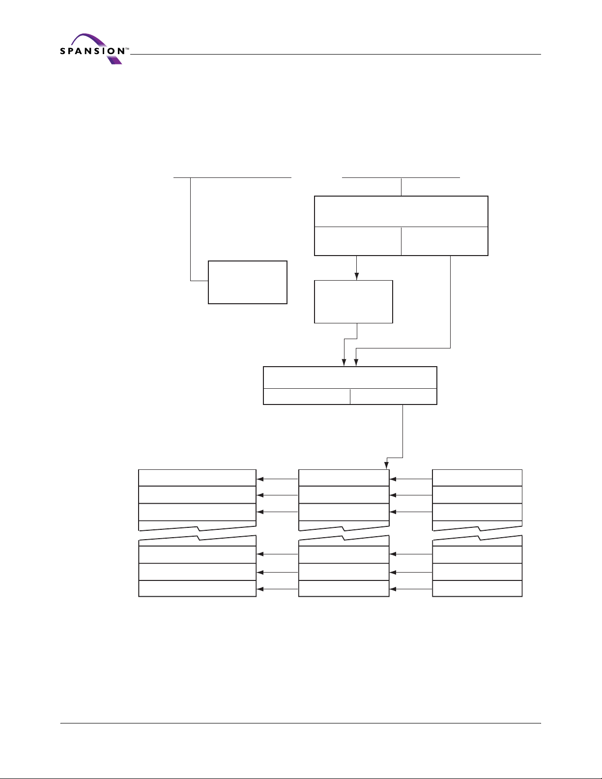
Preliminary
8 Advanced Sector Protection/Unprotection
The Advanced Sector Protection/Unprotection feature disables or enables programming or erase
operations in any or all sectors and can be implemented through software and/or hardware meth
ods, which are independent of each other. This section describes the various methods of
protecting data stored in the memory array . An overview of these met hods in shown in
Hardware Methods Software Methods
Lock Register
(One Time Programmable)
-
Figure 8.1.
WP# = V
(All boot
sectors locked)
Memory Array
Sector 0
Sector 1
Sector 2
Password Method
(DQ2)
IL
64-bit Password
(One Time Protect)
PPB Lock Bit
0 = PPBs Locked
Persistent
Protection Bit (PPD)
(Notes 5, 6)
PPB 0
PPB 1
PPB 2
Persistent Method
(DQ1)
(Notes 1, 2, 3)
1 = PPBs Unlocked
Dynamic
Protection Bit (DYB)
(Notes 7, 8, 9)
DYB 0
DYB 1
DYB 2
Sector N-2
Sector N-1
Sector N
Notes:
1. Bit is volatile, and defaults to 1 on reset.
2. Programming to 0 locks all PPBs to their current state.
3. Once programmed to 0, requires hardware reset to unlock.
4. N = Highest Address Sector.
5. 0 = Sector Protected,
1 = Sector Unprotected.
(Note 4)
PPB N-2
PPB N-1
PPB N
6. PPBs programmed individually, but cleared collectively.
7. 0 = Sector Protected,
1 = Sector Unprotected.
8. Protect effective only if PPB Lock Bit is unlocked and
corresponding PPB is 1 (unprotected).
9. Volatile Bits: defaults to user choice upon power-up
(see ordering options).
DYB N-2
DYB N-1
DYB N
Figure 8.1 Advanced Sector Protection/Unprotection
48 S29PL-N MirrorBit™ Flash Family S29PL-N_00_A4 November 23, 2005
Page 51

8.1 Lock Register
As shipped from the factory , all devices default to the persistent mode when power is applied, and
all sectors are unprotected, unless otherwise chosen through the DYB ordering option (see Or
dering Information). The device programmer or host system must then choose which sector
protection method to use. Programming (setting to 0) any one of t he following t wo one-time p ro
grammable, non-volatile bits locks the part permanently in that mod e:
Lock Register Persistent Protection Mode Lock Bit (DQ1)
Lock Register Password Protection Mode Lock Bit (DQ2)
Device DQ15 – 05 DQ4 DQ3 DQ2 DQ1 DQ0
S29PL256N Undefined
For programming lock register bits see Table 12.2.
Notes
1. If the password mode is chosen, the password must be programmed before setting the cor-
responding lock register bit.
2. After the Lock Register Bits Command Set Entry command sequence is written, reads and
writes for Bank A are disabled, while reads from other banks are allowed until exiting this
mode.
3. If both lock bits are selected to be programmed (to zeros) at the same time, the operation
aborts.
4. Once the Password Mode Lock Bit is programmed, the Persistent Mode Lock Bit is perma-
nently disabled, and no changes to the protection scheme are allowed. Similarly, if the
Persistent Mode Lock Bit is programmed, the Password Mode is permanently disabled.
After selecting a sector protection method, each sector can operate in any of the following three
states:
1. Constantly locked. The selected sec tors are protect ed and cannot b e reprogrammed unless
PPB lock bit is cleared via a password, hardware reset, or power cycle.
2. Dynamically locked. The selected sectors are protected and can be altered via software
commands.
3. Unlocked. The sectors are unprotected and can be erased and/or programmed.
These states are controlled by the bit types described in Sections 8.2 – 8.6.
Preliminary
Table 8.1 Lock Register
DYB Lock Boot Bit
0 = sectors
power up
protected
1 = sectors
power up
unprotected
PPB One-Time
Programmable Bit
0 = All PPB erase
command disabled
1 = All PPB Erase
command enabled
Password
Protection
Mode Lock Bit
Persistent
Protection
Mode Lock Bit
Secured
Silicon Sector
Protection Bit
-
-
8.2 Persistent Protection Bits
The Persistent Protection Bits are unique and nonvolatile for each sector and have the same endurances as the Flash memory. Preprogramming and verification prior to erasure are handled by
the device, and therefore do not require system monitoring.
November 23, 2005 S29PL-N_00_A4 S29PL-N MirrorBit™ Flash Family 49
Page 52

Notes
1. Each PPB is individually programmed and all are erased in parallel.
2. Entry command disables reads and writes for the bank selected.
3. Reads within that bank return the PPB status for that sector.
4. Reads from other banks are allowed while writes are not allowed.
5. All Reads must be performed using the Asynchronous mode.
6. The specific sector addresses (A23 – A14 PL256N and A22 – A14 PL127N/PL129N) are writ-
ten at the same time as the program command.
7. If the PPB Lock Bit is set, the PPB Program or erase command does not execute and times-
out without programming or erasing the PPB.
8. There are no means for individually erasing a specific PPB and no spe cific s ector addre ss is
required for this operation.
9. Exit command must be issued after the execution which resets the device to read mode and
re-enables reads and writes for Bank A.
10. The programming state of the PPB for a given sector can be v erified by writing a P PB Status
Read Command to the device as described by the flow chart below.
8.3 Dynamic Protection Bits
Dynamic Protection Bits are volatile and unique for each sector and can be individually modified.
DYBs only control the protection scheme for unprotected sectors that have their PPBs cleared
(erased to 1). By issuing the DYB Set or Clear command sequences, the DYBs are set (pro
grammed to 0) or cleared (erased to 1), thus placing each sector in the protected or unprotected
state respectively. This feature allows software to easily protect sectors against inadvertent
changes yet does not prevent the easy removal of protection when changes are needed.
Notes
1. The DYBs can be set (programmed to 0) or cleared (erased to 1) as often as needed. When
the parts are first shipped, the PPBs are cleared (erased to 1) and upon power up or reset, the DYBs can be set or cleared depending upon the ordering option chosen.
2. If the option to clear the DY Bs after power up i s chosen, (er ased to 1), then the sectorsmay
be modified depending upon the PPB state of that sector.
3. The sectors would be in the protected state If t he op tion t o set the DYBs afte r p ower up is
chosen (programmed to 0).
4. It is possible to have sectors that are persistently locked with sectors that are left in the
dynamic state.
5. The DYB Set or Clear commands for the dynamic sectors signify protected or unprotected
state of the sectors respectively . Howev er, if there is a need to change the status of the pe rsistently locked sectors, a few more steps are required. First, the PPB Lock Bit must be
cleared by either putting the device through a power-cycle, or hardware reset. The PPBs can
then be changed to reflect the desired settings. Setting the PPB Lock Bit once again locks
the PPBs, and the device operates normally again.
6. T o achiev e the best protection, it is recommended to execute the PPB Lock Bit Set command
early in the boot code and protect the boot code by holding WP# = V
and DYB bits have the same function when WP#/ACC = V
ACC = V
IH
.
Preliminary
. Note that the PPB
IL
as they do when WP#/
HH
-
8.4 Persistent Protection Bit Lock Bit
The Persistent Protection Bit Lock Bit is a global volatile bit for all sectors. When set (programmed
to 0), this bit locks all PPB and when cleared (programmed to 1), unlocks each sector. There is
only one PPB Lock Bit per device.
50 S29PL-N MirrorBit™ Flash Family S29PL-N_00_A4 November 23, 2005
Page 53

Preliminary
Notes
1. No software command sequence unlocks this bit unless the device is in the password pro-
tection mode; only a hardware reset or a power-up clears this bit.
2. The PPB Lock Bit must be set (programmed to 0) only after all PPBs are configured to the
desired settings.
8.5 Password Protection Method
The Password Protection Method allows an even higher level of security than the P ersistent Sector
Protection Mode by requiring a 64-bit password for unlocking the device PPB Lock Bit. In addition
to this password requirement, after power up and reset, the PPB Lock Bit is set 0 to maintain the
password mode of operation. Successful execution of the Password Unlock comma nd by enter ing
the entire password clears the PPB Lock Bit, allowing for sector PPBs modifications.
Notes
1. There is no special addressing order required for programming the password. Once the
Password is written and verified, the Password Mode Locking Bit must be set to prevent access.
2. The Password Program Command is only capable of programming 0s. Programming a 1
after a cell is programmed as a 0 results in a time-out with the cell as a 0.
3. The password is all 1s when shipped from the factory.
4. All 64-bit password combinations are valid as a password.
5. There is no means to verify what the password is after it is set.
6. The Password Mode Lock Bit, once set, prevents reading the 64-bit password on the data
bus and further password programming.
7. The Password Mode Lock Bit is not erasable.
8. The lower two address bits (A1 – A0) are valid during the Password Read, Password Pro-
gram, and Password Unlock.
9. The exact password must be entered in order for the unlocking function to occur.
10. The Password Unlock command cannot be issued any faster than 1 µs at a time to prevent
a hacker from running through all the 64-bit combinations in an attempt to correctly match
a password.
11. Approximately 1 µs is required for unlocking the device after the valid 64-bit password is
given to the device.
12. Password verification is only allowed during the password programming operation.
13. All further commands to the password region are disabled and all operations are ignored.
14. If the password is lost after setting the Password Mode Lock Bit, there is no way to clear the
PPB Lock Bit.
15. Entry command sequence must be issued prior to any of any oper ation and it disables reads
and writes for Bank A. Reads and writes for other banks excluding Bank A are allowed.
16. If the user attempts to program or erase a protected sector, the device ignores the com-
mand and returns to read mode.
17. A program or erase command to a protected sector enables status po lling and returns to
read mode without having modified the contents of the protected sector.
18. The programming of the DYB, PPB, and PPB Lock for a given sector can be verified by writing
individual status read commands DYB Status, PPB Status, and PPB Lock Status to the
device.
November 23, 2005 S29PL-N_00_A4 S29PL-N MirrorBit™ Flash Family 51
Page 54

Preliminary
Write Unlock Cycles:
Address 555h, Data AAh
Address 2AAh, Data 55h
Enter Lock Register Command:
Address 555h, Data 40h
Program Lock Register Data
Address XXXh, Data A0h
Address 77h*, Data PD
Perform Polling Algorithm
(see Write Operation Status
Yes
Write
Wait 4 µs
flowchart)
Done?
No
Unlock Cycle 1
Unlock Cycle 2
XXXh = Address don’t care
* Not on future devices
Program Data (PD): See text for Lock Register
definitions
Caution: Lock data may only be progammed once.
PASS. Write Lock Register
Exit Command:
Address XXXh, Data 90h
Address XXXh, Data 00h
Device returns to reading array.
Figure 8.2 Lock Register Program Algorithm
DQ5 = 1?
Yes
No
FAIL. Write rest command
to return to reading array.
Error condition (Exceeded Timing Limits)
52 S29PL-N MirrorBit™ Flash Family S29PL-N_00_A4 November 23, 2005
Page 55
Preliminary
8.6 Advanced Sector Protection Software Examples
Table 8.2 Sector Protection Schemes
Sector PPB
Unique Device PPB Lock Bit
0 = locked, 1 = unlocked
Any Sector 0 0 x Protected through PPB
Any Sector 0 0 x Protected through PPB
Any Sector 0 1 1 Unprotected
Any Sector 0 1 0 Protected through DYB
Any Sector 1 0 x Protected through PPB
Any Sector 1 0 x Protected through PPB
Any Sector 1 1 0 Protected through DYB
Any Sector 1 1 1 Unprotected
0 = protected
1 = unprotected
Table 8.2 contains all possible combinations of the DYB, PPB, and PPB Lock Bit relating to the sta-
tus of the sector. In summary, if the PPB Lock Bit is locked (set to 0), no changes to the PPBs are
allowed. The PPB Lock Bit can only be unlocked (reset to 1) through a hardware reset or power
cycle. See also
Figure 8.1 for an overview of the Advanced Sector Protection feature.
8.7 Hardware Data Protection Methods
The device offers data protection at the sector level via hardware control:
When WP#/ACC is at VIL, the four outermost sectors are locked (device specific).
There are additional methods by which intended or accidental erasure of any sectors can be prevented via hardware means. The following subsections describes these methods:
Sector DYB
0 = protected
1 = unprotected Sector Protection Status
8.7.1 WP# Method
The Write Protect feature provides a hardware method of protecting the four outermost sectors.
This function is provided by the WP#/ACC pin and overrides the previously discussed Sector Pro
tection/Unprotection method.
If the system asserts VIL on the WP#/ACC pin, the de vice disables program and erase functions
in the outermost boot sectors. The outermost boot sectors are the sectors containing both the
lower and upper set of sectors in a dual-boot-configured device.
If the system asserts VIH on the WP#/ACC pin, the device reverts to whether the boot sectors
were last set to be protected or unprotected. That is, sector protection or unprotection for these
sectors depends on whether they were last protected or unprotected.
Note that the WP#/ACC pin must not be left floating or unconnected as inconsistent behavior of
the device may result.
The WP#/ACC pin must be held stable during a command sequence execution
8.7.2 Low VCC Write Inhibit
When VCC is less than V
V
power-up and power-down.
CC
The command register and all internal program/erase circuits are disabled, and t he device resets
to reading array data. Subsequent writes are ignored until V
must provide the proper signals to the control inputs to prevent unintention al wri tes when V
greater than V
LKO
LKO
.
, the device does not accept any write cycles. This protects data during
is greater than V
CC
. The system
LKO
CC
is
-
November 23, 2005 S29PL-N_00_A4 S29PL-N MirrorBit™ Flash Family 53
Page 56

8.7.3 Write Pulse Glitch Protection
Noise pulses of less than 3 ns (typical) on OE#, CE# or WE# do not initiate a write cycle.
8.7.4 Power-Up Write Inhibit
If WE# = CE# = RESET# = VIL and OE# = VIH during power up, the device does not accept commands on the rising edge of WE#. The internal state machine is automatically reset to the read
mode on powerup.
Preliminary
54 S29PL-N MirrorBit™ Flash Family S29PL-N_00_A4 November 23, 2005
Page 57

Preliminary
9 Power Conservation Modes
9.1 Standby Mode
When the system is not reading or writing to the device, it can place the device in the standby
mode. In this mode, current consumption is greatly reduced, and the outputs are placed in the
high impedance state, independent of the OE# input. The device enters the C MOS standby mode
when the CE# and RESET# inputs are both held at V
cess time (tCE) for read access, before it is ready to read data. If the device is deselected during
erasure or programming, the device draws active current until the operation is completed. I
in DC Characteristics represents the standby current specification
9.2 Automatic Sleep Mode
The automatic sleep mode minimizes Flash device energy consumption while in asynchronous
mode. the device automatically enables this mode when addresses remain stable for t
The automatic sleep mode is independent of the CE#, WE#, and OE# control signals. Standard
address access timings provide new data when addresses are changed. While in sleep mode, out
put data is latched and always available to the system. I
automatic sleep mode current specification.
9.3 Hardware RESET# Input Operation
±0.2 V. The device requires standard ac-
CC
+ 20 ns.
ACC
in DC Characteristics represents the
CC6
CC3
-
The RESET# input provides a hardware method of resetting the device to reading array data.
When RESET# is driven low for at least a period of t
operation in progress, tristates all outputs, resets the configuration register, and ignores all read/
write commands for the duration of the RESET# pulse. The device also resets the internal state
machine to reading array data. The operation that was interrupted should be reinitiated once the
device is ready to accept another command sequence to ensure data integrity.
When RESET# is held at VSS ±0.2 V, the device draws CMOS standby current (I
is held at V
RESET# may be tied to the system reset circuitry and thus, a system reset would also reset the
Flash memory, enabling the system to read the boot-up firmware from the Flash memory.
but not within VSS ±0.2 V, the standby current is greater.
IL
9.4 Output Disable (OE#)
When the OE# input is at VIH, output from the device is disabled. The outputs are placed in the
high impedance state.
, the device immediately terminates any
RP
). If RESET#
CC4
November 23, 2005 S29PL-N_00_A4 S29PL-N MirrorBit™ Flash Family 55
Page 58
Preliminary
10 Secured Silicon Sector Flash Memory Region
The Secured Silicon Sector provides an extra Flash memory region that enables permanent part
identification through an Electronic Serial Number (ESN). The Secured Silicon Sector is 256 words
in length that consists of 128 words for factory data and 128 words f or customer -secured a reas.
All Secured Silicon reads outside of the 256-word address range returns invalid data. The Factory
Indicator Bit, DQ7, (at Autoselect address 03h) is used to indicate whether or not the F actor y Se
cured Silicon Sector is locked when shipped from the factory. The Customer Indicator Bit (DQ6)
is used to indicate whether or not the Customer Secured Silicon Sector is locked when shipped
from the factory.
Note the following general conditions:
While the Secured Silicon Sector access is enabled, simultaneous operations are allowed ex-
cept for Bank A.
On power up, or following a hardware reset, the device reverts to sending commands to the
normal address space.
Reads outside of sector 0 return memory array data.
Sector 0 is remapped from the memory array to the Secured Silicon Sector array.
Once the Secured Silicon Sector Entry Command is issued, the Secured Silicon Sector Exit
command must be issued to exit Secured Silicon Sector Mode.
The Secured Silicon Sector is not accessible when the device is executing an Embedded Pro-
gram or Embedded Erase algorithm.
-
Table 10.1 Secured Silicon Sector Addresses
Sector Sector Size Address Range
Customer 128 words 000080h-0000FFh
Factory 128 words 000000h-00007Fh
10.1 Factory Secured Silicon Sector
The Factory Secured Silicon Sector is always protected when shipped from the factory and has
the Factory Indicator Bit (DQ7) permanently set to a 1. This prevents cloning of a factory locked
part and ensures the security of the ESN and customer code once the product is shipped to the
field.
These devices are available pre programmed with one of the following:
A random, 8-word secure ESN only within the Factory Secured Silicon Sector
Customer code within the Customer Secured Silicon Sector through the Spansion
ming service.
Both a random, secure ESN and customer code through the Spansion programming service.
Customers may opt to have their code programmed through the Spansion progr amming services.
Spansion programs the customer's code, with or without the random ESN. The devices are then
shipped from the Spansion factory with the Factory Secured Silicon Sector and Customer Secured
Silicon Sector permanently locked. Contact your local representative for details on using Spansion
programming services.
TM
program-
56 S29PL-N MirrorBit™ Flash Family S29PL-N_00_A4 November 23, 2005
Page 59

Preliminary
10.2 Customer Secured Silicon Sector
The Customer Secured Silicon Sector is typically shipped unprotected (DQ6 set to 0), allowing
customers to utilize that sector in any manner they choose. If the security feature is not required,
the Customer Secured Silicon Sector can be treated as an additional Flash memory space.
Please note the following:
Once the Customer Secured Silicon Sector area is protected, the Customer Indicator Bit is
permanently set to 1.
The Customer Secured Silicon Sector can be read any number of times, but can be pro-
grammed and locked only once. The Customer Secured Sili con Sector lock must be used with
caution as once locked, there is no procedure available for unlocking the Customer Secured
Silicon Sector area and none of the bits in the Customer Secured Silicon Sector memory space
can be modified in any way.
The accelerated programming (ACC) and unlock bypass functions are not available when pro-
gramming the Customer Secured Silicon Sector, but are available when reading in Banks B
through D.
Once the Customer Secured Silicon Sector is locked and verified, the system must write the
Exit Secured Silicon Sector Region command sequence which return the device to the mem-
ory array at sector 0.
10.3 Secured Silicon Sector Entry and Exit Command Sequences
The system can access the Secured Silicon Sector region by issuing the three-cycle Enter Secured
Silicon Sector command sequence. The device continues to access the Secured Silicon Sector re
gion until the system issues the four-cycle Exit Secured Silicon Sector command sequence.
See the Command Definition Tables
Table 12.1, Memory Array Commands.
Table 12.2, Sector Protection Commands for address and data requirements for both command
sequences.
The Secured Silicon Sector Entry Command allows the following commands to be executed
Read customer and factory Secured Silicon areas
Program the customer Secured Silicon Sector
After the system has written the Enter Secured Silicon Sector command sequence, it may read
the Secured Silicon Sector by using the addresses normally occupied by sector SA0 within the
memory array. This mode of operation continues until the system issues the Exit Secured Silicon
Sector command sequence, or until power is removed from the device.
Software Functions and Sample Code
The following are C functions and source code examples of using the Secured Silicon Sector
Entry, Program, and exit commands. Refer to the Spansion Low Level Driver User Guide
(available soon on www .amd.com and www.fujitsu.com) for general information on Spansion
Flash memory software development guidelines.
-
November 23, 2005 S29PL-N_00_A4 S29PL-N MirrorBit™ Flash Family 57
Page 60
Preliminary
Table 10.2 Secured Silicon Sector Entry
(LLD Function = lld_SecSiSectorEntryCmd)
Cycle Operation Word Address Data
Unlock Cycle 1 Write Base + 555h 00AAh
Unlock Cycle 2 Write Base + 2AAh 0055h
Entry Cycle Write Base + 555h 0088h
Note: Base = Base Address.
/* Example: SecSi Sector Entry Command */
*((UINT16 *)base_addr + 0x555) = 0x00AA; /* write unlock cycle 1 */
*((UINT16 *)base_addr + 0x2AA) = 0x0055; /* write unlock cycle 2 */
*((UINT16 *)base_addr + 0x555) = 0x0088; /* write Secsi Sector Entry Cmd */
Table 10.3 Secured Silicon Sector Program
(LLD Function = lld_ProgramCmd)
Cycle Operation Word Address Data
Unlock Cycle 1 Write Base + 555h 00AAh
Unlock Cycle 2 Write Base + 2AAh 0055h
Program Setup Write Base + 555h 00A0h
Program Write Word Address Data Word
Note: Base = Base Address.
/* Once in the SecSi Sector mode, you program */
/* words using the programming algorithm. */
Table 10.4 Secured Silicon Sector Exit
(LLD Function = lld_SecSiSectorExitCmd)
Cycle Operation Word Address Data
Unlock Cycle 1 Write Base + 555h 00AAh
Unlock Cycle 2 Write Base + 2AAh 0055h
Exit Cycle Write Base + 555h 0090h
Note: Base = Base Address.
/* Example: SecSi Sector Exit Command */
*((UINT16 *)base_addr + 0x555) = 0x00AA; /* write unlock cycle 1 */
*((UINT16 *)base_addr + 0x2AA) = 0x0055; /* write unlock cycle 2 */
*((UINT16 *)base_addr + 0x555) = 0x0090; /* write SecSi Sector Exit cycle 3 */
*((UINT16 *)base_addr + 0x000) = 0x0000; /* write SecSi Sector Exit cycle 4 */
58 S29PL-N MirrorBit™ Flash Family S29PL-N_00_A4 November 23, 2005
Page 61
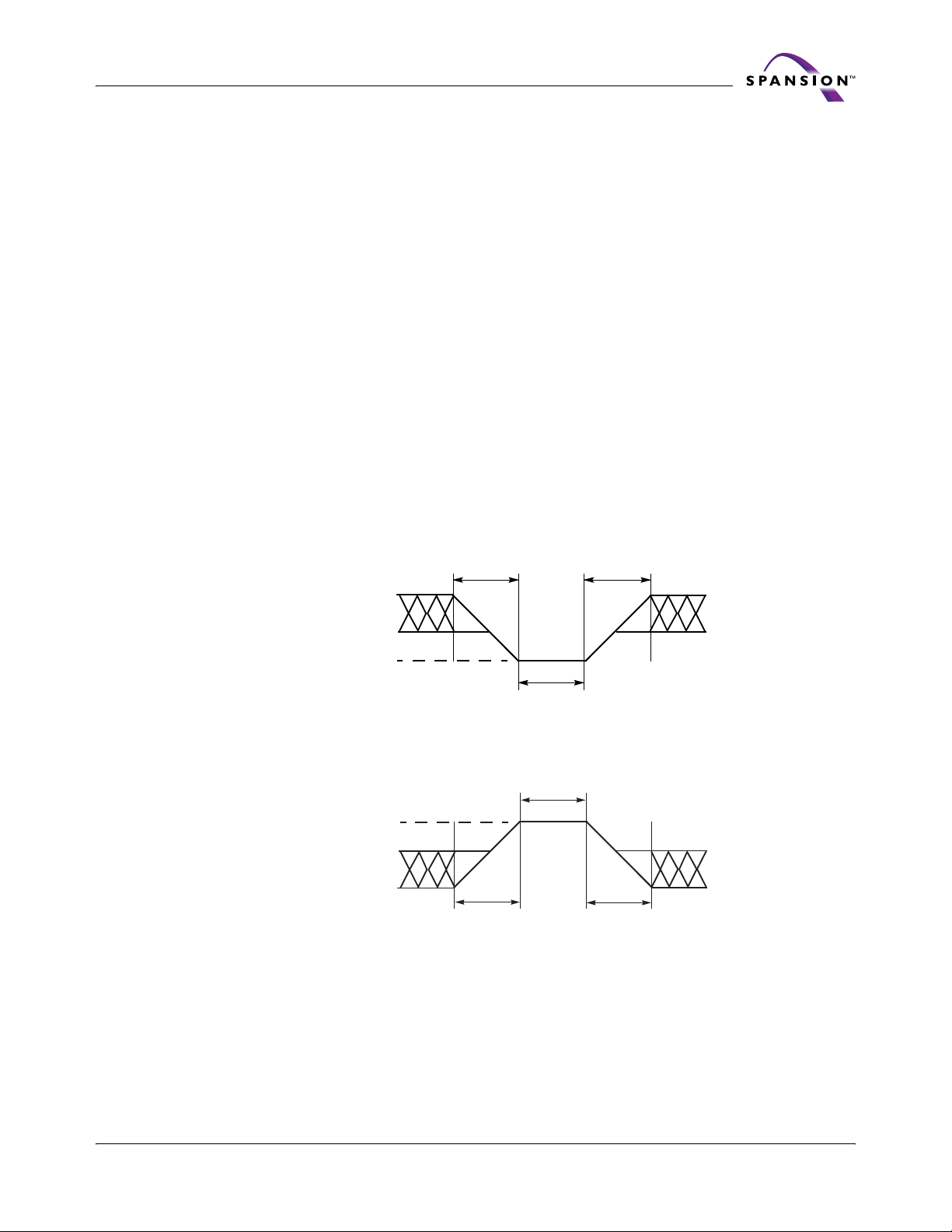
Preliminary
11 Electrical Specifications
11.1 Absolute Maximum Ratings
Storage Temperature
Plastic Packages . . . . . . . . . . . . . . . . . . . . . . . . . . . . . . . . . . . . . . . . . . . . . . . . . . . –65°C to +150°C
Ambient Temperature
with Power Applied . . . . . . . . . . . . . . . . . . . . . . . . . . . . . . . . . . . . . . . . . . . . . . . . . –65°C to +125°C
Voltage with Respect to Ground:
All Inputs and I/Os except as noted below (Note 1). . . . . . . . . . . . . . . . . . . . . . . . –0.5 V to VIO + 0.5 V
VCC (Note 1). . . . . . . . . . . . . . . . . . . . . . . . . . . . . . . . . . . . . . . . . . . . . . . . . . . . . . .–0.5 V to +4.0 V
VIO (Note 1) . . . . . . . . . . . . . . . . . . . . . . . . . . . . . . . . . . . . . . . . . . . . . . . . . . . . . . . –0.5 V to +4.0V
ACC (Note 2) . . . . . . . . . . . . . . . . . . . . . . . . . . . . . . . . . . . . . . . . . . . . . . . . . . . . .–0.5 V to +10.5 V
Output Short Circuit Current (Note 3) . . . . . . . . . . . . . . . . . . . . . . . . . . . . . . . . . . . . . . . . . . . 200 mA
Notes:
1. Minimum DC voltage on input or I/Os is –0.5 V. Duri ng voltage transitions, inputs or I/Os may undershoot VSS to –2.0 V
for periods of up to 20 ns. See Figure 11.1. Maximum DC voltage on input or I/Os is V
transitions outputs may overshoot to V
2. Minimum DC input voltage on pin WP#
for periods of up to 20 ns. See Figure 11.1. Maximum DC voltage on pin WP#
10.5 V for periods up to 20 ns.
3. No more than one output may be shorted to ground at a time. Durat i on of the short circuit should not be gr eater than
one second.
4. Stresses above those listed under Absolute Maximum Ratings may cause permanent damage to the device. This is a
stress rating only; functional operation of the device at these or any other conditions above those indicated in the
operational sections of this data sheet is not implied. Exposure of th e devic e to abso lu te m aximu m ra tin g co n ditio ns for
extended periods may affect device reliability.
+ 0.5 V. During voltage
+ 2.0 V for periods up to 20 ns. See Figure 11.2.
CC
⁄
ACC is –0.5 V. During voltage transitions, WP#⁄ACC may overshoot VSS to 2.0 V
CC
⁄
ACC is +9.5 V, which may overshoot to
20 ns
20 ns
+0.8 V
–0.5 V
–2.0 V
20 ns
Figure 11.1 Maximum Negative Overshoot Waveform
20 ns
V
CC
+2.0 V
V
CC
+0.5 V
2.0 V
20 ns
20 ns
Figure 11.2 Maximum Positive Overshoot Waveform
November 23, 2005 S29PL-N_00_A4 S29PL-N MirrorBit™ Flash Family 59
Page 62

11.2 Operating Ranges
L
Wireless (W) Devices
Ambient Temperature (TA) . . . . . . . . . . . . . . . . . . . . . . . . . . . . . . . . . . . . . . . . . . . . . –25°C to +85°C
Industrial (I) Devices
Ambient Temperature (TA) . . . . . . . . . . . . . . . . . . . . . . . . . . . . . . . . . . . . . . . . . . . . . –40°C to +85°C
Supply Voltages
VCC Supply Voltages . . . . . . . . . . . . . . . . . . . . . . . . . . . . . . . . . . . . . . . . . . . . . . . .+2.7 V to 3.1 V or
. . . . . . . . . . . . . . . . . . . . . . . . . . . . . . . . . . . . . . . . . . . . . . . . . . . . . . . . . . . . . . +2.7 V to +3.6 V
Notes:
1. Operating ranges define those limits between which the functionality of the device is guaranteed.
2. For all AC and DC specifications, V
3. Voltage range of 2.7 – 3.1 V valid for PL-N MCP products.
11.3 Test Conditions
Preliminary
= VCC.
IO
Device
Under
Test
(Note 3)
C
Output Load Capacitance, CL (including jig capacitance) 30 pF
Input Rise and Fall Times V
Input Pulse Lev els V
Input timing measurement reference levels V
Output timing measurement reference levels V
11.4 Key to Switching Waveforms
WAVEFORM INPUTS OUTPUTS
Don’t Care, Any Change Permitted Changing, State Unknown
Figure 11.3 Te st S e t u p
Table 11.1 Test Specifications
Test Condition All Speeds Unit
= 3.0 V 5 ns
CC
= 3.0 V 0.0 – 3.0 V
CC
/2 V
CC
/2 V
CC
Steady
Changing from H to L
Changing from L to H
Does Not Apply
Center Line is High Impedance State
(High Z)
60 S29PL-N MirrorBit™ Flash Family S29PL-N_00_A4 November 23, 2005
Page 63
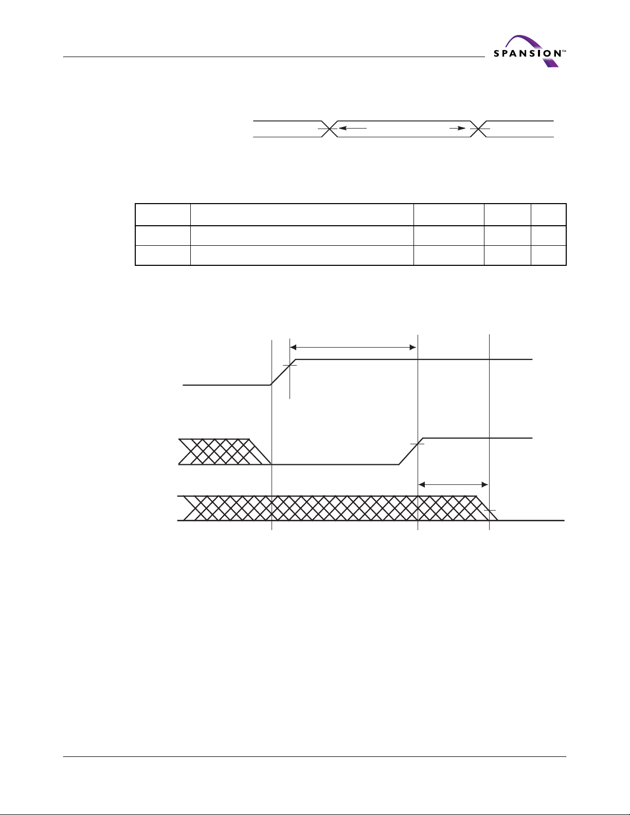
Preliminary
11.5 Switching Waveforms
Figure 11.4 Input Waveforms and Measurement Levels
11.6 VCC Power U p
Parameter Description Test Setup Speed Unit
V
0.0 V
IO
VCC/2 VCC/2All Inputs and Outputs
OutputMeasurement LevelInput
t
VCS
t
READ
Notes:
1. VCC ramp rate must exceed 1 V/400 µs.
2. V
is internally connected to VCC.
IO
V
CC
Time between RESET# high and CE# low Min 200 ns
VCC Setup Time Min 250 µs
RESET#
CE#
t
VCS
V
CC
min
V
IH
t
Read
Figure 11.5 VCC Power-Up Diagram
November 23, 2005 S29PL-N_00_A4 S29PL-N MirrorBit™ Flash Family 61
Page 64
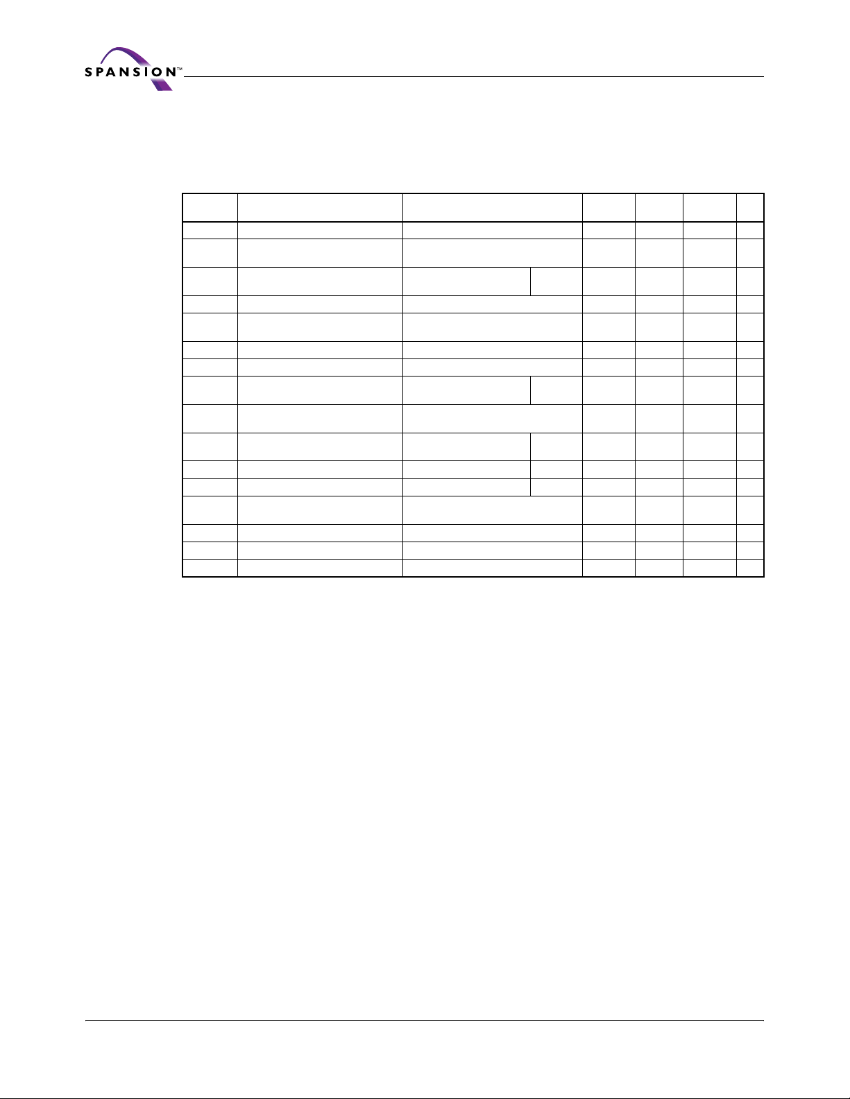
11.7 DC Characteristics
11.7.1 DC Characteristics (VCC = 2.7 V to 3.6 V)
(CMOS Compatible)
Preliminary
Parameter
Symbol
I
LI
I
LO
I
CC1
I
CC2
I
CC3
I
CC4
I
CC5
I
CC6
I
CC7
I
CC8
V
IL
V
IH
V
HH
V
OL
V
OH
V
LKO
Parameter Description
(Notes)
Test Conditions
Input Load Current VIN = VSS to VCC, VCC = VCC
V
= VSS to VCC, OE# = V
Output Leakage Current
VCC Active Read Current (1, 3)
VCC Active Write Current (3)OE# = VIH, WE# = V
VCC Standby Current
VCC Reset Current RESET# = V
Automatic Sleep Mode (4)V
VCC Active Read-While-Write
Current (1)
VCC Active Program-While-Erase-
Suspended Current (5)
VCC Active Page Read Current
OUT
VCC = V
OE# = V
= V
V
CC
CE# (7), RESET#,
WP#/ACC = V
= V
IH
OE# = V
OE# = V
OE# = V
Page Read
(6)
CC max
,
IH
(1, 6)
CC max
± 0.3 V
CC
± 0.3 V 300 500 µA
SS
±0.3 V; VIL = V
CC
IH
IH
, 8 word
IH
IL
SS
max
IH
5 MHz 30 45 mA
± 0.3 V 20 40 µA
5 MHz 35 50 mA
40 MHz
Min
(Note 2)
(6)±2.0µA
Input Low Voltage VCC = 2.7 to 3.6 V –0.5 0.8 V
Input High Voltage VCC = 2.7 to 3.6 V 2.0 VCC + 0.3 V
Voltage for ACC Program
Acceleration
Output Low Voltage IOL = 100 µA, VCC = V
Output High Voltage IOH = –100 µA (6)V
= 3.0 V ±10% (6)8.59.5V
V
CC
(6)0.1V
CC min
CC
Low VCC Lock-Out Voltage (5)2.32.5V
Notes:
1. The ICC current listed is typically less than 5 mA/MHz, with OE# at VIH.
2. Maximum I
=3.0 V, TA = +25°C.
V
CC
3. I
is active while Embedded Erase or Embedded Program is in progress.
CC
4. Automatic sleep mode enables the low power mode when addresses remain stable for t
current is 1 µA.
5. Not 100% tested.
6. The data in the table is for V
7. CE1# and CE2# for the PL129N.
specifications are tested with VCC = V
CC
range 2.7 V to 3.6 V (recommended for standalone applications).
CC
max, TA = TAmax. Typical I
CC
CC
Ty p
(Note 2)
Max Unit
±1.0 µA
25 50 mA
20 40 µA
27 55 mA
610mA
– 0.2 V
specifications are with typical
+30 ns. Typical sleep mode
ACC
62 S29PL-N MirrorBit™ Flash Family S29PL-N_00_A4 November 23, 2005
Page 65
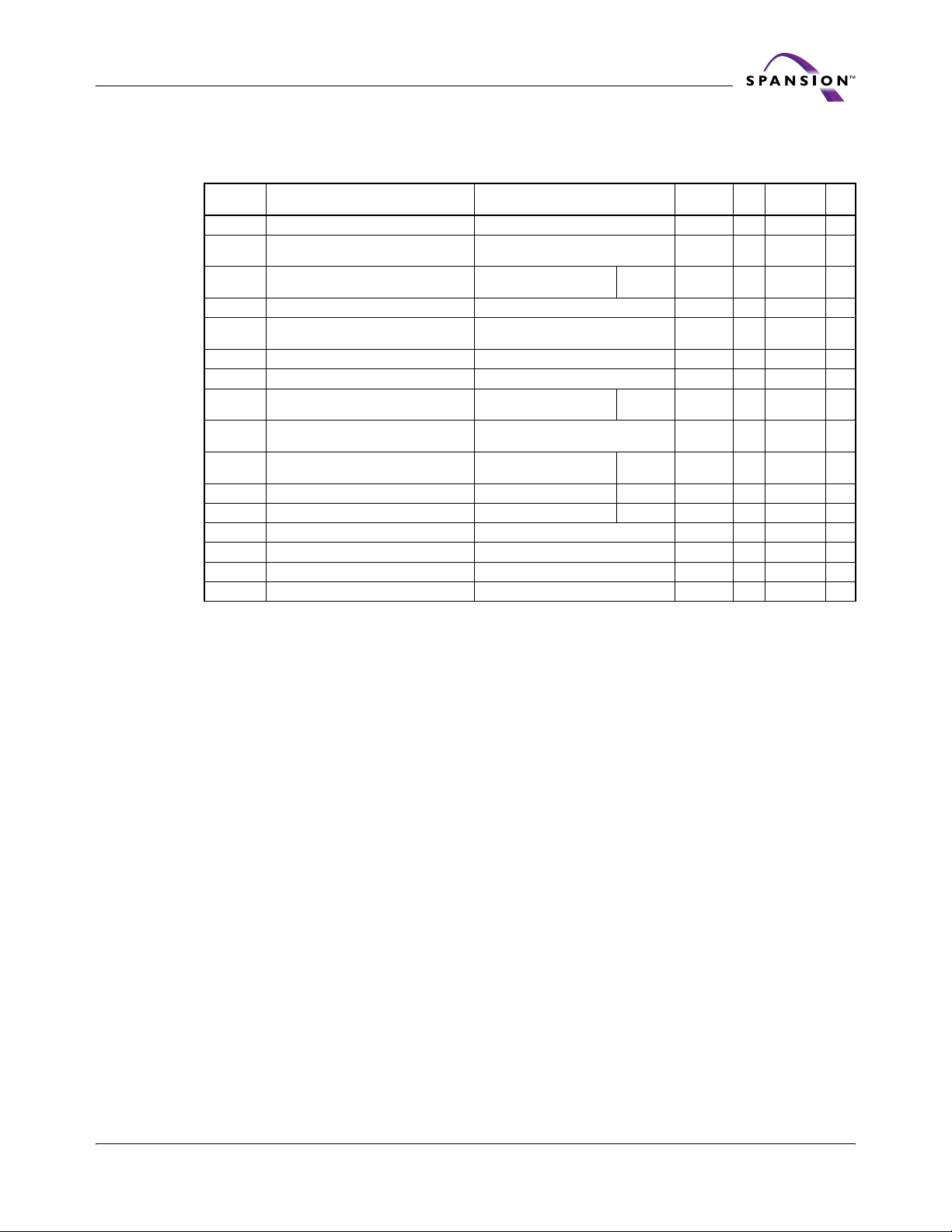
Preliminary
11.7.2 DC Characteristics (VCC = 2.7 V to 3.1 V)
(CMOS Compatible)
Paramet er
Symbol
I
LI
I
LO
I
CC1
I
CC2
I
CC3
I
CC4
I
CC5
I
CC6
I
CC7
I
CC8
V
IL
V
IH
V
HH
V
OL
V
OH
V
LKO
Parameter Description
(Notes)
Input Load Current VIN = VSS to VCC, VCC = VCC
V
Output Leakage Current
VCC Active Read Current (1, 2)
OUT
VCC = V
OE# = V
V
CC
VCC Active Write Current (2, 3)OE# = V
VCC Standby Current (2)
CE# (7), RESET#, WP#/ACC
= V
VCC Reset Current (2) RESET# = V
Automatic Sleep Mode (2, 4)V
VCC Active Read-While-Write
Current (1, 2)
VCC Active Program-While-Erase-
Suspended Current (2, 5)
VCC Active Page Read Current (2)
IH
OE# = V
OE# = V
OE# = V
8 word Page Read
Test Conditions Min Typ Max Unit
(6)±2µA
max
= VSS to VCC, OE# = V
= V
CC
= V
(6)
CC max
,
IH
(1, 6)
CC max
, WE# = V
IH
± 0.3 V
SS
±0.3 V; VIL = V
CC
IH
IH
,
IH
± 0.3 V 300 500 µA
IH
5 MHz 28 40 mA
IL
± 0.1 V 20 40 µA
SS
5 MHz 33 45 mA
40 MHz 6 9 mA
Input Low Voltage VCC = 2.7 to 3.6 V –0.5 0.8 V
Input High Voltage VCC = 2.7 to 3.6 V 2.0 VCC + 0.3 V
Voltage for ACC Program Acceleration VCC = 3.0 V ±10% (6)8.59.5V
Output Low Voltage IOL = 100 µA, VCC = V
(6)0.1V
CC min
Output High Voltage IOH = –100 µA (6)V
Low VCC Lock-Out Voltage (5)2.32.5V
Notes:
1. The ICC current listed is typically less than 5 mA/MHz, with OE# at VIH.
2. Maximum I
=2.9 V, TA = +25°C.
V
CC
3. I
active while Embedded Erase or Embedded Program is in progress.
CC
4. Automatic sleep mode enables the low power mode when addresses remain stable for t
current is 1 µA.
5. Not 100% tested.
6. Data in table is for V
7. CE1# and CE2# for the PL129N.
specifications are tested with VCC = V
CC
range 2.7 V to 3.1 V (recommended for MCP applications)
CC
max, TA = TAmax. Typical I
CC
CC
±1 µA
22 40 mA
20 40 µA
24 45 mA
– 0.2 V
CC
specifications are with typical
+ 30 ns. Typical sleep mode
ACC
November 23, 2005 S29PL-N_00_A4 S29PL-N MirrorBit™ Flash Family 63
Page 66
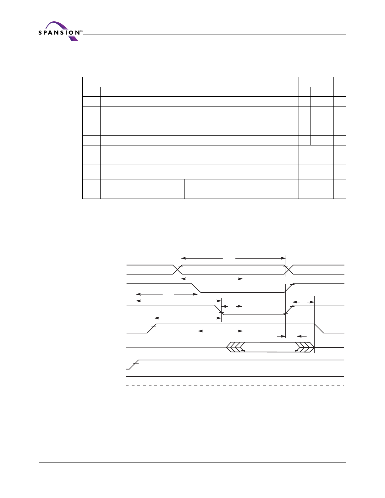
11.8 AC Characteristics
11.8.1 Read Operations
Preliminary
Parameter
JEDEC Std. 65 70 80 Unit
t
AVAVtRC
t
AVQVtACC
t
ELQVtCE
t
GLQVtOE
t
EHQZtDF
t
GHQZtDF
t
AXQXtOH
Read Cycle Time (1) Min 65 70 80 ns
Address to Output Delay CE#, OE# = VILMax 65 70 80 ns
Chip Enable to Output Delay (5) OE # = V
t
Page Access Time Max 25 30 30 ns
PACC
Output Enable to Output Delay Max 25 30 30 ns
Chip Enable to Output High Z (3)Max16ns
Output Enable to Output High Z (1, 3)Max16ns
Output Hold Time From Addresses, CE# or OE#,
Whichever Occurs First (3)
t
Output Enable Hold Time (1)
OEH
Description
(Notes)
Read Min 0 ns
T o ggle and Data# Polling Min 10 ns
Notes:
1. Not 100% tested.
2. See Figure 11.3 and Table 11.1 for test specifications
3. Measurements performed by placing a 50 ohm termination on the data pin with a bias of V
high to the data bus driven to V
4. For 70pf Output Load Capacitance, 2 ns is added to the above t
5. CE1# and CE2# for the PL129N.
/2 is taken as tDF.
CC
11.8.2 Read Operation Timing Diagrams
Addresses
CE#
OE#
WE#
Data
t
RH
t
RH
t
OEH
HIGH Z
ACC
t
RC
Addresses Stable
t
ACC
t
OE
t
CE
,tCE ,t
Te s t S e tu p
,t
PACC
IL
OE
Max 65 70 80 ns
Min 5 ns
/2. The time from OE#
CC
values for all speed grades
t
t
OH
Valid Data
Speed Options
DF
HIGH Z
RESET#
RY/BY#
0 V
Figure 11.6 Read Operation Timings
64 S29PL-N MirrorBit™ Flash Family S29PL-N_00_A4 November 23, 2005
Page 67
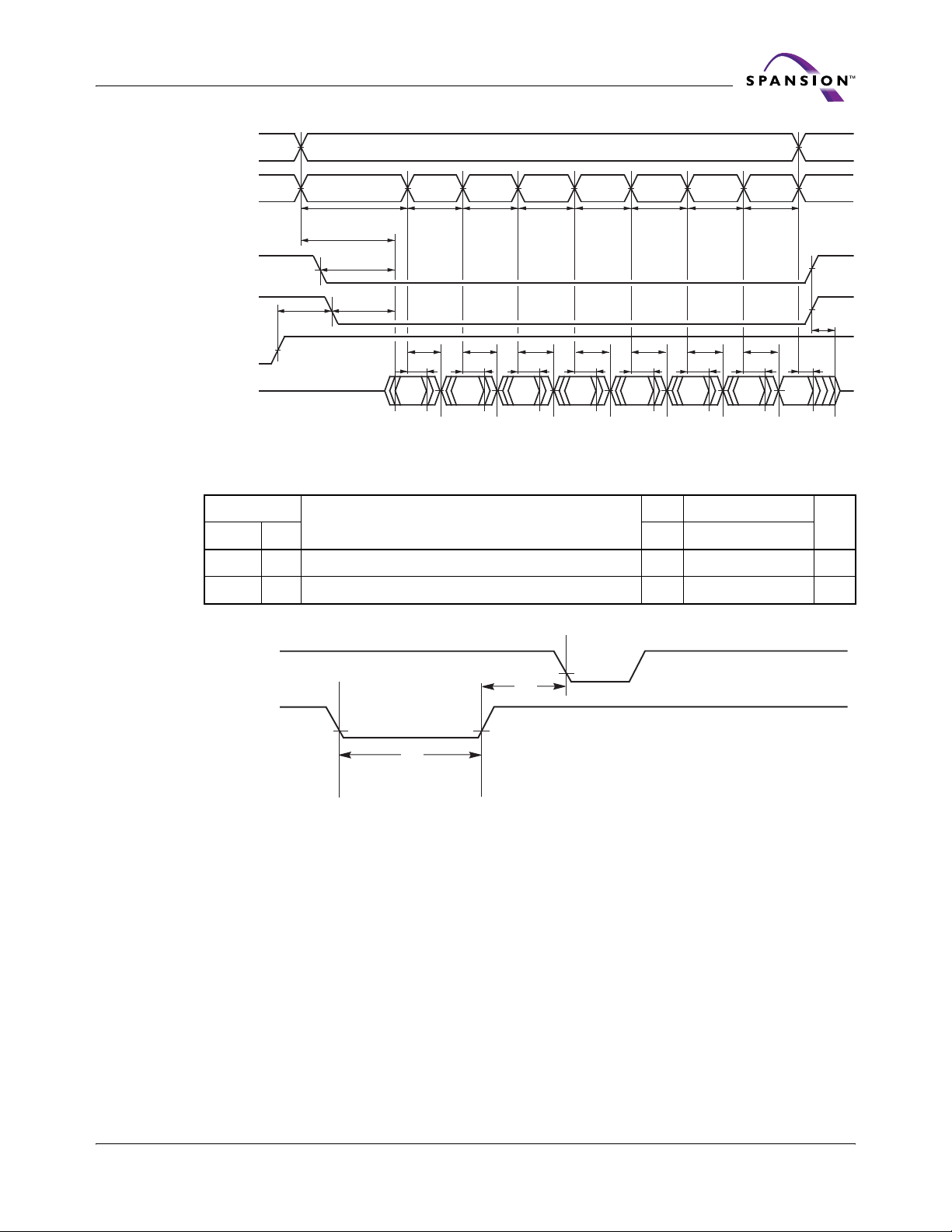
A22 to A
A2 to A
CE#
Preliminary
3
0
Aa Aa+1 Aa+2 Aa+3 Aa+4 Aa+5 Aa+6 Aa+7
t
ACC
t
CE
Same page Addresses
OE#
WE#
Output
t
OEH
High-Z
t
OE
t
PACC
t
OH
Da Da+1 Da+2 Da+7
Figure 11.7 Page Read Operation Timings
11.8.3 Hardware Reset (RESET#)
Parameter
JEDEC Std.
tRPRESET# Pulse Width Min 30 µs
Reset High Time Before Read (See Note)Min200ns
t
RH
Note: Not 100% tested.
CE#, OE#
RESET#
t
PACC
t
OH
Description
t
DF
t
PACC
t
OH
t
PACC
t
OH
Da+3 Da+4 Da+5 Da+6
t
PACC
t
OH
t
PACC
t
OH
t
PACC
t
OH
t
OH
All Speed Options
Unit
t
RH
t
RP
Figure 11.8 Reset Timings
November 23, 2005 S29PL-N_00_A4 S29PL-N MirrorBit™ Flash Family 65
Page 68
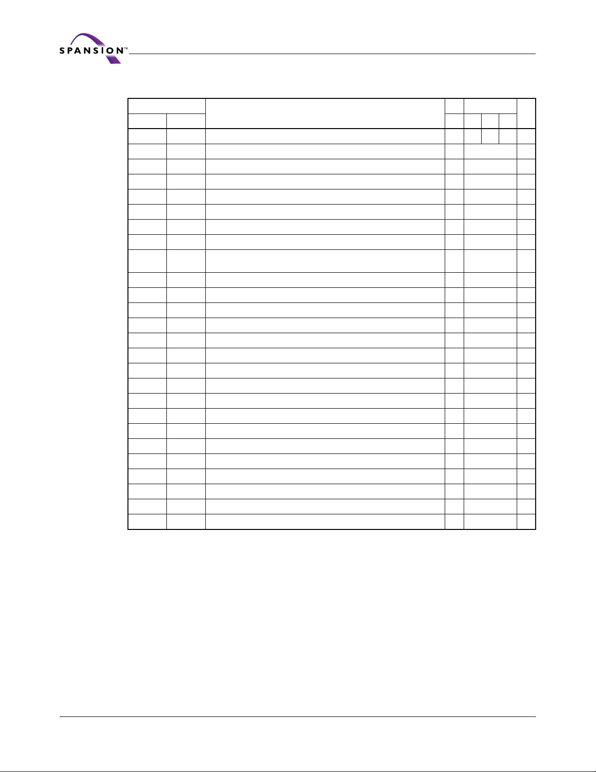
11.8.4 Erase/Program Timing
Preliminary
Parameter
JEDEC Std 65 70 80
t
AVAV
t
AVWL
t
WLAX
t
DVWH
t
WHDX
t
GHWL
t
ELWL
t
WHEH
t
WLWH
t
WHDL
t
WHWH1tWHWH1
t
WHWH1tWHWH1
t
WHWH2tWHWH2
t
WC
t
AS
t
ASO
t
AH
t
AHT
t
DS
t
DH
t
OEPH
t
GHWL
t
CS
t
CH
t
WP
t
WPH
t
SR/W
t
VHHVHH
t
RB
t
BUSY
t
WEP
t
SEA
t
ESL
t
PSL
t
ASP
t
PSP
Write Cycle Time (1) Min 65 70 80 ns
Address Setup Time Min 0 ns
Address Setup Time to OE# low during toggle bit polling Min 15 ns
Address Hold Time Min 35 ns
Address Hold Time From CE# or OE# high during toggle bit polling Min 0 ns
Data Setup Time Min 30 ns
Data Hold Time Min 0 ns
Output Enable High during toggle bit polling Min 10 ns
Read Recovery Time Before Write
(OE# High to WE# Low)
CE# Setup Time Min 0 ns
CE# Hold Time Min 0 ns
Write Pulse Width Min 40 ns
Write Pulse Width High Min 25 ns
Latency Between Read and Write Operations Min 0 ns
Programming Operation Typ 40 µs
Accelerated Programming Operation Typ 24 µs
Sector Erase Operation Typ 1.6 sec
Rise and Fall Times Min 250 ns
Write Recovery Time from RY/BY# Min 0 ns
Program/Erase Valid to RY/BY# Delay Max 90 ns
Noise Pulse Margin on WE# Max 3 ns
Sector Erase Accept Time-out Max 50 µs
Erase Suspend Latency Max 20 µs
Program Suspend Latency M ax 20 µs
Toggle Time During Sector Protection Typ 100 µs
Toggle Time During Programming Within a Protected Sector Typ 1 µs
Description (Notes)
Speed Options
Min 0 ns
Notes:
1. Not 100% tested.
2. In program operation timing, addresses are latched on the falling edge of WE#.
3. See Program/Erase Operations for more information.
4. Does not include the preprogramming time.
Unit
66 S29PL-N MirrorBit™ Flash Family S29PL-N_00_A4 November 23, 2005
Page 69

Preliminary
Program Command Sequence (last two cycles)
t
WC
Addresses
CE#
555h
t
CH
OE#
t
WP
WE#
t
WPH
t
DH
Data
t
CS
t
DS
A0h
RY/BY#
V
CC
t
VCS
Note: PA = program address, PD = program data, D
Read Status Data (last two cycles)
t
AS
PA PA
t
AH
PD
t
BUSY
is the true data at the program address
OUT
t
WHWH1
PA
Status
D
OUT
t
RB
WP#/ACC
Figure 11.9 Program Operation Timings
V
HH
V
or V
IL
IH
t
VHH
t
VHH
VIL or V
IH
Figure 11.10 Accelerated Program Timing Diagram
November 23, 2005 S29PL-N_00_A4 S29PL-N MirrorBit™ Flash Family 67
Page 70
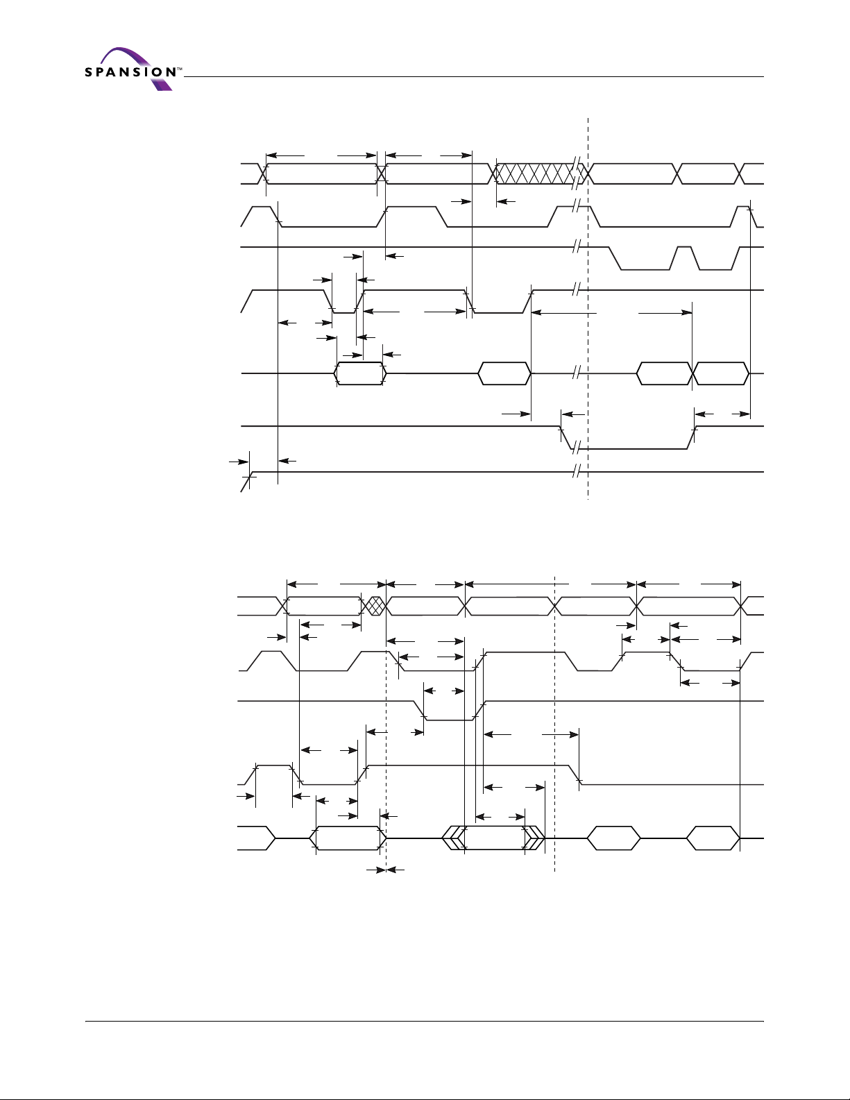
Preliminary
Erase Command Sequence (last two cycles) Read Status Data
t
AS
555h for chip erase
VA
t
AH
VA
Addresses
t
WC
2AAh SA
CE#
t
OE#
WE#
Data
t
CS
CH
t
WP
t
WPH
t
DS
t
DH
55h
30h
10 for Chip Erase
t
BUSY
t
WHWH2
Status D
t
OUT
RB
RY/BY#
t
VCS
V
CC
Note: SA = sector address (for Sector Erase), VA = Valid Address for reading stat us dat a (see Write Operation Status)
Figure 11.11 Chip/Sector Erase Operation Timings
Addresses
CE#
OE#
WE#
Data
t
WC
Valid PA
t
t
AS
t
WPH
AH
t
WP
t
DS
t
DH
Valid
In
t
OEH
t
RC
Valid RA
t
ACC
t
CE
t
SR/W
t
OE
t
OH
Valid
Out
Read Cycle
t
DF
t
GHWL
t
WC
Valid PA
Valid
In
CE# Controlled Write CyclesWE# Controlled Write Cycle
t
CPH
t
WC
Valid PA
t
AS
t
AH
t
CP
Valid
In
Figure 11.12 Back-to-back Read/Write Cycle Timings
68 S29PL-N MirrorBit™ Flash Family S29PL-N_00_A4 November 23, 2005
Page 71
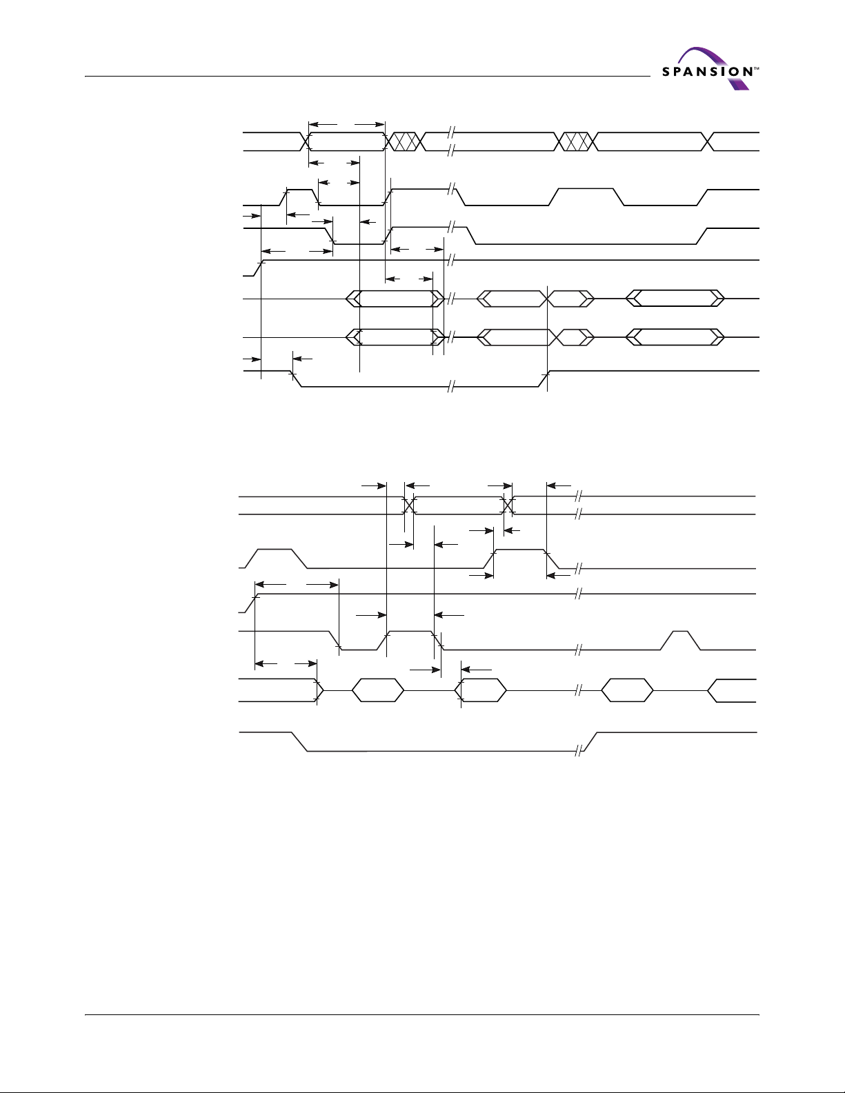
Addresses
CE#
OE#
WE#
DQ7
Preliminary
t
RC
VA
t
ACC
t
CE
t
CH
t
OEH
t
OE
t
OH
Complement
VA VA
t
DF
Complement
Tr ue
Valid Data
High Z
DQ6–DQ0
t
BUSY
Status Data
Status Data
Tr ue
Valid Data
High Z
RY/BY#
Note: VA = Valid address. Illustration shows first sta tus c ycle after command sequence, last status read cycle, and array
data read cycle
Figure 11.13 Data# Polling Timings (During Embedded Algorithms)
t
AHT
Addresses
t
ASO
CE#
t
OEH
WE#
t
OEPH
OE#
t
DH
DQ6/DQ2 Valid Data
Valid Data
Valid
Status
t
OE
Valid
Status
(first read) (second read) (stops toggling)
t
CEPH
t
t
AS
AHT
Valid
Status
RY/BY#
Note: VA = Valid address; not required for DQ6. Illustration shows first two status cycle after comma nd sequence, last
status read cycle, and array data read cycle
Figure 11.14 Toggle Bit Timings (During Embedded Algorithms)
November 23, 2005 S29PL-N_00_A4 S29PL-N MirrorBit™ Flash Family 69
Page 72
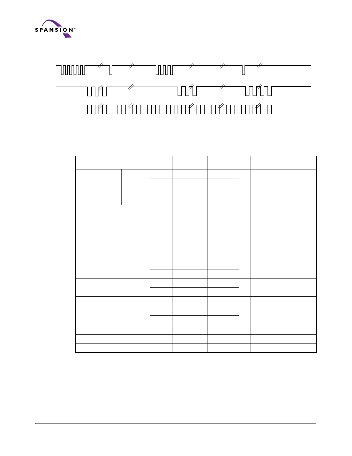
Preliminary
Enter
Embedded
Erasing
WE#
Erase
Erase
Suspend
Erase Suspend
Enter Erase
Suspend Program
Read
DQ6
DQ2
Note: DQ2 toggles only when read at an address wi th in an erase-suspended sector. The system may use OE# or CE# to
toggle DQ2 and DQ6.
Figure 11.15 DQ2 vs. DQ6
11.8.5 Erase and Programming Performance
Parameter
(Notes)
128 Kword
Sector Erase Time
32 Kword
Chip Erase Time
Word Programming Time
Effective Word Programming Time
utilizing Program Write Buffer
Total 32-Word Buffer
Programming Time
Chip Programming Time
using 32-Word Bu ffe r ( 3)
Erase Suspend/Erase Resume <20 µs
Program Suspend/Program Resume <20 µs
Device
Condition
V
CC
ACC 1.6 7
V
CC
ACC 0.3 4
V
CC
ACC
V
CC
ACC 24 240
V
CC
ACC 6 60
V
CC
ACC 192 1920
V
CC
ACC
Erase
Suspend
Program
Ty p
(Note 1)
1.6 7
0.3 4
202 (PL256N)
100 (PL127N)
100(PL129N)
130 (PL256N)
65 (PL127N)
65 (PL129N)
9.4 94
300 3000
157.3 (PL256N)
78.6 (PL127N)
78.6 (PL129N)
100 (PL256N)
50 (PL127N)
50 (PL129N)
Erase Suspend
Read
Max
(Note 2)
900 (PL256N)
450 (PL127N)
450 (PL129N)
512 (PL256N)
256 (PL127N)
256 (PL129N)
40 400
315 (PL256N)
158 (PL127N)
158 (PL129N)
200 (PL256N)
100 (PL127N)
100 (PL129N)
Erase
Resume
Unit
s
s
µs
µs
µs
s
Erase
Comments
Excludes 00h programming
prior to erasure (4)
Excludes system level overhead
(5)
Excludes system level overhead
(5)
Erase
Complete
(Notes)
Notes:
1. Typical program and erase times assume the following conditions: 25°C, 3.0 V VCC, 10,000 cycles. Additionally,
programming typicals assume checkerboard pattern. All values are subject to change.
2. Under worst case conditions of 90°C, V
3. The typical chip programming time is considerably less than the maximum chip programming time listed, since most
bytes program faster than the maximum program times listed.
4. In the pre-programming step of the Embedded Erase algorithm, all bytes are programmed to 00h before erasure.
5. System-level overhead is the time re quired to execute the two- or four-bus-cycle sequence for the program command.
See Table 12.1 and Table 12.2 for further information on command definitions.
6. Contact the local sales office for minimum cycling endurance values in specific applications and operating conditions.
7. See Application Note Erase Suspend/Resume Timing for more details.
8. Word programming specification is based upon a single word programming operation not utilizing the write buffer.
= 2.7 V, 100,000 cycles. All values are subject to change.
CC
70 S29PL-N MirrorBit™ Flash Family S29PL-N_00_A4 November 23, 2005
Page 73

Preliminary
11.8.6 BGA Ball Capacitance
Parameter
Symbol
C
IN
C
OUT
C
IN2
Notes:
1. Sampled, not 100% tested.
2. Test conditions T
= 25°C, f = 1.0 MHz.
A
Parameter Description Test Setup Typ Max Unit
Input Capacitance VIN = 0 7 10 pF
Output Capacitance V
Control Pin Capacitance VIN = 0 8 11 pF
= 0 8 12 pF
OUT
November 23, 2005 S29PL-N_00_A4 S29PL-N MirrorBit™ Flash Family 71
Page 74

Preliminary
72 S29PL-N MirrorBit™ Flash Family S29PL-N_00_A4 November 23, 2005
Page 75

Preliminary
12 Appendix
This section contains information relating to software control or interfacing with the Flash device.
For additional information and assistance regarding software, see
plore the Web at www.amd.com and www.fujitsu.com.
Table 12.1 Memory Array Commands
Command Sequence
(Notes)
Read (7)1RARD
Reset (8)1XXXF0
Program 4 555 AA 2AA 55 555 A0 PA Data
Write to Buffer (17) 6 555 AA 2AA 55 SA 25 SA WC PA PD WBL PD
Program Buffer to Flash 1 SA 29
Write to Buffer Abort Reset (17) 3 555 AA 2AA 55 555 F0
Chip Erase 6 555 AA 2AA 55 555 80 555 AA 2AA 55 555 10
Sector Erase 6 555 AA 2AA 55 555 80 555 AA 2AA 55 SA 30
Program/Erase Suspend (14) 1 BA B0
Program/Erase Resume (15)1BA30
CFI Query (16) 1 [BA]555 98
Unlock
Bypass
Secured Silicon Sector Command Definitions
Secured
Manufacturer ID 4 555 AA 2AA 55 [BA]555 90 [BA]X00 0001
Auto-
Device ID (10) 6 555 AA 2AA 55 [BA]555 90 [BA]X01 227E [BA]X0E
select
(9)
Indicator Bits 4 555 AA 2AA 55 [BA]555 90 [BA]X03
Unlock Bypass Entry 3 555 AA 2AA 55 555 20
Unlock Bypass Program (12, 13)2XXA0PAPD
Unlock Bypass Sector Erase (12, 13)2 XX 80 SA 30
Unlock Bypass Erase (12, 13) 2 XX 80 XXX 10
Mode
Unlock Bypass CFI (12, 13)1BA98
Unlock Bypass Reset 2 XX 90 XXX 00
Secured Silicon Sector Entry (18) 3 555 AA 2AA 55 555 88
Secured Silicon Sector Program 2 XX A0 PA data
Silicon
Secured Silicon Sector Read 1 RA data
Sector
Secured Silicon Sector Exit (19) 4 555 AA 2AA 55 555 90 XX 00
First Second Third Fourth Fifth Sixth
Cycles
Addr Data Addr Data Addr Data Addr Data Addr Data Addr Data
Bus Cycles (Notes 1 – 6)
Additional Resources, or ex-
(Note
[BA]X0F 2200
(Note
11)
10)
Legend:
X = Don’t care.
RA = Read Address.
RD = Read Data.
PA = Address of the memory location to be programmed. Addresses
latch on the falling edge of the WE# or CE# pulse whichever
happens later.
PD = Program Data. Data latches on the rising edge of WE# or CE#
pulse, whichever occurs first.
Notes:
1. See (Table 7.1) for description of bus operations.
2. All values are in hexadecimal.
3. Except for the following, all bus cycles are write cycle: read
cycle, fourth through sixth cycles of the Autoselect commands,
fourth cycle of the password verify command, and any cycle
reading at RD(0) and RD(1).
4. Data bits DQ15 – DQ8 are don’t care in command sequences,
except for RD, PD, WD, PWD, and PWD3 – PWD0.
5. Unless otherwise noted, these address bits are don’t cares:
PL127: A22 – A15; 129N: A21 – A15; PL256N: A23 – A14.
6. Writing incorrect address and data values or writing them in the
improper sequence may place the device in an unknow n state.
The system must write the reset command to return the device
to reading array data.
7. No unlock or command cycles required when bank is reading
array data.
8. The Reset command is required to return to reading array data
(or to the erase-suspend-read mode if previously in Erase
Suspend) when a bank is in the autoselect mode, or if DQ5 goes
high (while the bank is providing status information) or
performing sector lock/unlock.
SA = Sector Address. PL127/129N = A22 – A15;
PL256N = A23 – A15.
BA = Bank Address. PL256N = A23 – A21; PL127N = A22 – A20;
PL127N = A21 – A20.
WBL = Write Buffer Location. Address must be within the same write
buffer page as PA.
WC = Word Count. Number of write buffer locations to load minus 1.
9. The fourth cycle of the autoselect command sequence is a read
cycle. The system must provide the bank address. See
Autoselect.
10. Device IDs: PL256N = 223Ch; PL127N = 2220h;
PL129N = 2221h.
11. See Autoselect.
12. The Unlock Bypass command sequence is required prior to this
command sequence.
13. The Unlock Bypass Reset command is required to return to
reading array data when the bank is in the unlock bypass mode.
14. The system may read and program in non-erasing sectors, or
enter the autoselect mode, when in the Erase Suspend mode.
The Erase Suspend command is valid only during a sector erase
operation, and requires the bank address.
15. The Erase Resume command is valid only during the Erase
Suspend mode, and requires the bank address.
16. The total number of cycles in the command sequence is
determined by the number of words written to the write buffer.
The maximum number of cycles in the command sequence is 37.
November 23, 2005 S29PL-N_00_A4 S29PL-N MirrorBit™ Flash Family 73
Page 76
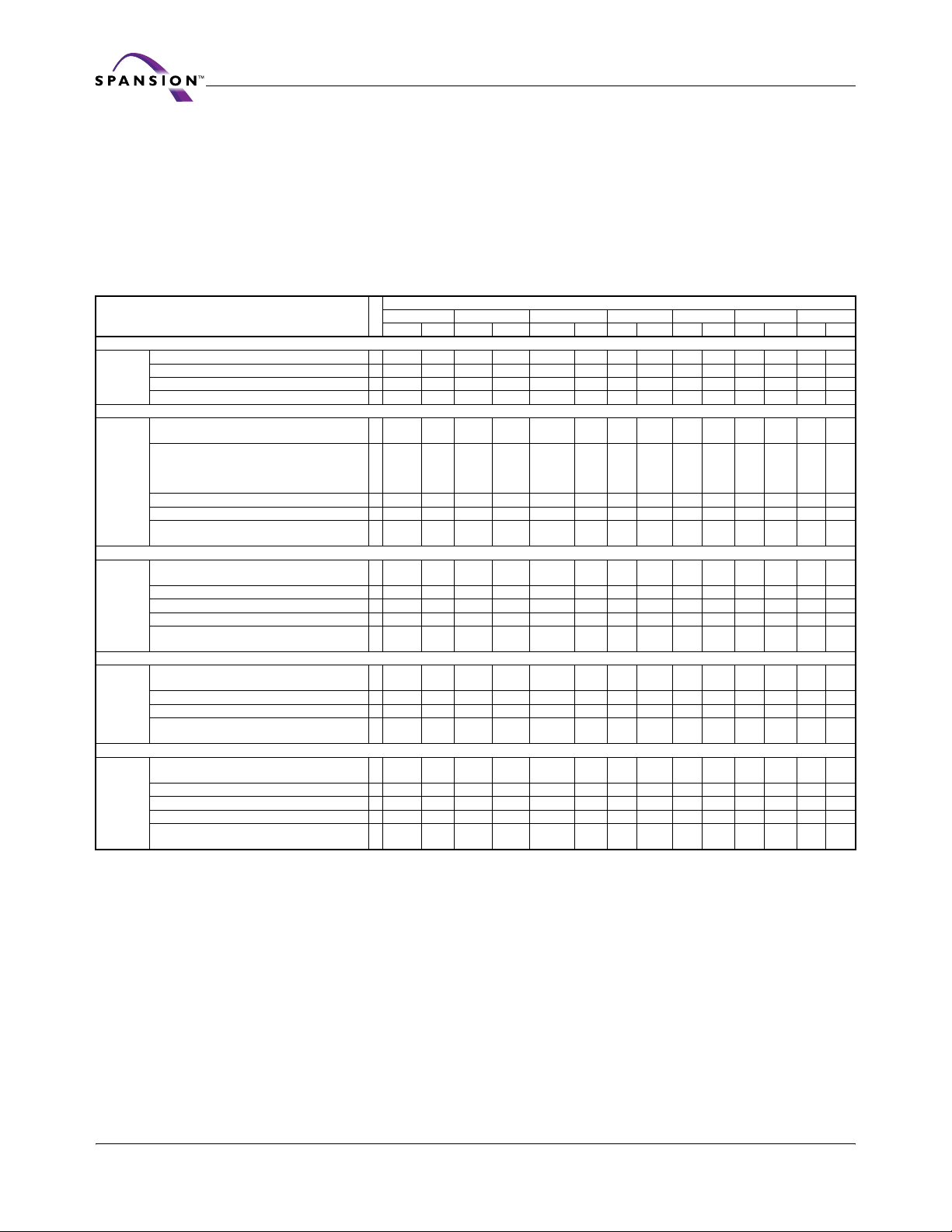
Preliminary
17. Command sequence resets device for next command after writeto-buffer operation.
18. Entry commands are needed to enter a specific mode to enable
instructions only available within that mode.
19. The Exit command must be issued to reset the device into read
mode. Otherwise the device hangs.
20. The following mode cannot be performed at the same time.
Autoselect/CFI/Unlock Bypass/Secured Silicon. Command
sequence resets device for next command after write-to-buffer
operation.
Table 12.2 Sector Protection Commands
Command Sequence
(Notes)
Lock Register Command Set Definitions
Register
Password Protection Command Set Definitions
Password
Non-Volatile Sector Protection Command Set Definitions
Global Non-Volatile Sector Protection Freeze Command Set Definitions
PPB Lock
Volatile Sector Protection Command Set Definitions
Lock Register Command Set Entry (25)
Lock Register Bits Program (26)
Lock
Lock Register Bits Read
Lock Register Command Set Exit (27)
Password Protection
Command Set Entry (25)
Password Program
Passwo rd Read
Password Unlock
Password Protection
Command Set Exit (27)
Non-Volatile Sector Protection
Command Set Entry (25)
PPB Program
All PPB Erase (22)
PPB
PPB Status Read
Non-Volatile Sector Protection
Command Set Exit (27)
Global Volatile Sector Protection Freeze
Command Set Entry (25)
PPB Lock Bit Set
Bit
PPB Lock Bit Status Read
Global Volatile Sector Protection Freeze
Command Set Exit (27)
Volatile Sector Protection
Command Set Entry (25)
DYB Set
DYB Clear
DYB
DYB Status Read
Volatile Sector Protection
Command Set Exit (27)
First Second Third Fourth Fifth Sixth Seventh
Cycles
Addr Data Addr Data Addr Data Addr Data Addr Data Addr Data Addr Data
3 555 AA 2AA 55 555 40
2XX A0 00 data
100 data
2XX 90 XX 00
3 555 AA 2AA 55 555 60
2XX A0
4 00 PWD0 01 PWD1 02 PWD2 03 PWD3
7 00 25 00 03 00 PWD001PWD102PWD203PWD300 29
2XX 90 XX 00
3 555 AA 2AA 55 [BA]555 C0
2XX A0[BA]SA00
2XX 80 00 30
1[BA]SARD(0)
2XX 90 XX 00
3 555 AA 2AA 55 555 50
2XX A0 XX 00
1BARD(0)
2XX 90 XX 00
3 555 AA 2AA 55 [BA]555 E0
2XX A0[BA]SA00
2XX A0[BA]SA01
1[BA]SARD(0)
2XX 90 XX 00
21. Command is valid when device is ready to read array data or
when device is in autoselect mode. Address equals 55h on all
future devices, but 555h for PL256N.
22. Requires Entry command sequence prior to execution. Secured
Silicon Sector Exit Reset command is required to exit this mode;
device may otherwise be placed in an unknown state.
Bus Cycles (Notes 1 – 6)
PWD0/
00/01
PWD1/
02/03
PWD2/
PWD3
Legend:
X = Don’t care
RA = Read Address.
RD = Read Data.
PA = Address of the memory location to be programmed. Addresses
latch on the falling edge of the WE# or CE# pulse whichever
happens later.
PD = Program Data. Data latches on the rising edge of WE# or CE#
pulse, whichever occurs first.
SA = Sector Address. PL127/129N = A22 – A15; PL256N = A23 –
A15
BA = Bank Address. PL256N = A23 – A21; PL127N = A22 – A20;
PL127N = A21 – A20.
WBL = Write Buffer Location. Address must be within the same write
buffer page as PA.
WC = Word Count. Number of write buffer locations to load minus 1.
PWD3 – PWD0 = Password Data. PD3 – PD0 present four 16 bit
combinations that represent the 64-bit Password
RD(0) = DQ0 protection indicator bit. If protected, DQ0 = 0, if
unprotected, DQ0 = 1.
74 S29PL-N MirrorBit™ Flash Family S29PL-N_00_A4 November 23, 2005
Page 77

Preliminary
Notes:
1. See (Table 7.1) for description of bus operations.
2. All values are in hexadecimal.
3. Except for the following, all bus cycles are write cycle: read
cycle, fourth through sixth cycles of the Autoselect commands,
and password verify commands, and any cycle reading at RD(0)
and RD(1).
4. Data bits DQ15 – DQ8 are don’t care in command sequences,
except for RD, PD, WD, PWD, and PWD3 – PWD0.
5. Unless otherwise noted, these address bits are don’t cares:
PL127: A22 – A15; 129N: A21 – A15; PL256N: A23 – A14.
6. Writing incorrect address and data values or writing them in the
improper sequence may place the device in an unknow n state.
The system must write the reset command to return the device
to reading array data.
7. No unlock or command cycles required when bank is reading
array data.
8. The Reset command is required to return to reading array data
(or to the erase-suspend-read mode if previously in Erase
Suspend) when a bank is in the autoselect mode, or if DQ5 goes
high (while the bank is providing status information) or
performing sector lock/unlock.
9. The fourth cycle of the autoselect command sequence is a read
cycle. The system must provide the bank address. See
Autoselect.
10. The data is 0000h for an unlocked sector and 0001h for a locked
sector.
11. Device IDs: PL256N = 223Ch; PL127N = 2220h;
PL129N = 2221h.
12. See Autoselect.
13. The Unlock Bypass command sequence is required prior to this
command sequence.
14. The Unlock Bypass Reset command is required to return to
reading array data when the bank is in the unlock bypass
mode.The system may read and program in non-erasing sectors,
or enter the autoselect mode, when in the Erase Suspend mode.
The Erase Suspend command is valid only during a sector erase
operation, and requires the bank address.
15. The Erase Resume command is valid only during the Erase
Suspend mode, and requires the bank address.
16. Command is valid when device is ready to read array data or
when device is in autoselect mode.The total number of cycles in
the command sequence is determined by the number of w ords
written to the write buffer. The maximum number of cycles in
the command sequence is 37.
17. The entire four bus-cycle sequence must be entered for which
portion of the password.
18. The Unlock Bypass Reset command is required to return to
reading array data when the bank is in the unlock bypass
mode.The system may read and program in non-erasing sectors,
or enter the autoselect mode, when in the Erase Suspend mode.
The Erase Suspend command is valid only during a sector erase
operation, and requires the bank address.
19. The Erase Resume command is valid only during the Erase
Suspend mode, and requires the bank address.
20. Command is valid when device is ready to read array data or
when device is in autoselect mode.The total number of cycles in
the command sequence is determined by the number of w ords
written to the write buffer. The maximum number of cycles in
the command sequence is 37.
21. The entire four bus-cycle sequence must be entered for which
portion of the password.
22. The ALL PPB ERASE command pre-programs all PPBs before
erasure to prevent over-erasure of PPBs.
23. WP#/ACC must be at VHH during the entire operation of this
command.
24. Command sequence resets device for next command after writeto-buffer operation.
25. Entry commands are need ed to enter a specific mode to enable
instructions only available within that mode.
26. If both the Persistent Protection Mode Locking Bit and the
password Protection Mode Locking Bit are set a the same time,
the command operation aborts and returns the device to the
default Persistent Sector Protection Mode.
27. The Exit command must be issued to reset the device into read
mode. Otherwise the device hangs.
12.1 Common Flash Memory Interface
The Common Flash Interface (CFI) specification outlines device and host system software interrogation handshake, which allows specific vendor-specified soft-ware algorithms to be used for
entire families of devices. Software support can then be device-independent, JEDEC ID-indepen
dent, and forward- and back-ward-compatible for the specified flash device families. Flash
vendors can standardize their existing interfaces for long-term compatibility.
This device enters the CFI Query mode when the system writes the C FI Query command, 98h, to
address (BA)555h any time the device is ready to read array data. The system can read CFI in
formation at the addresses given in Tables 12.3 – 12.6) within that bank. All reads outside of the
CFI address range, within the bank, return non-valid data. Reads from other banks are allowed,
writes are not. To terminate reading CFI data, the system must write the reset command.
The following is a C source code example of using the CFI Entry and Exit functions. Refer to
the Spansion Low Level Driver User’s Guide (available at www.amd.com and
www.fujitsu.com) for general information on Spansion Flash memory software development
guidelines.
/* Example: CFI Entry command */
*((UINT16 *)bank_addr + 0x555) = 0x0098; /* write CFI entry command */
/* Example: CFI Exit command */
*((UINT16 *)bank_addr + 0x000) = 0x00F0; /* write cfi exit command */
-
-
November 23, 2005 S29PL-N_00_A4 S29PL-N MirrorBit™ Flash Family 75
Page 78
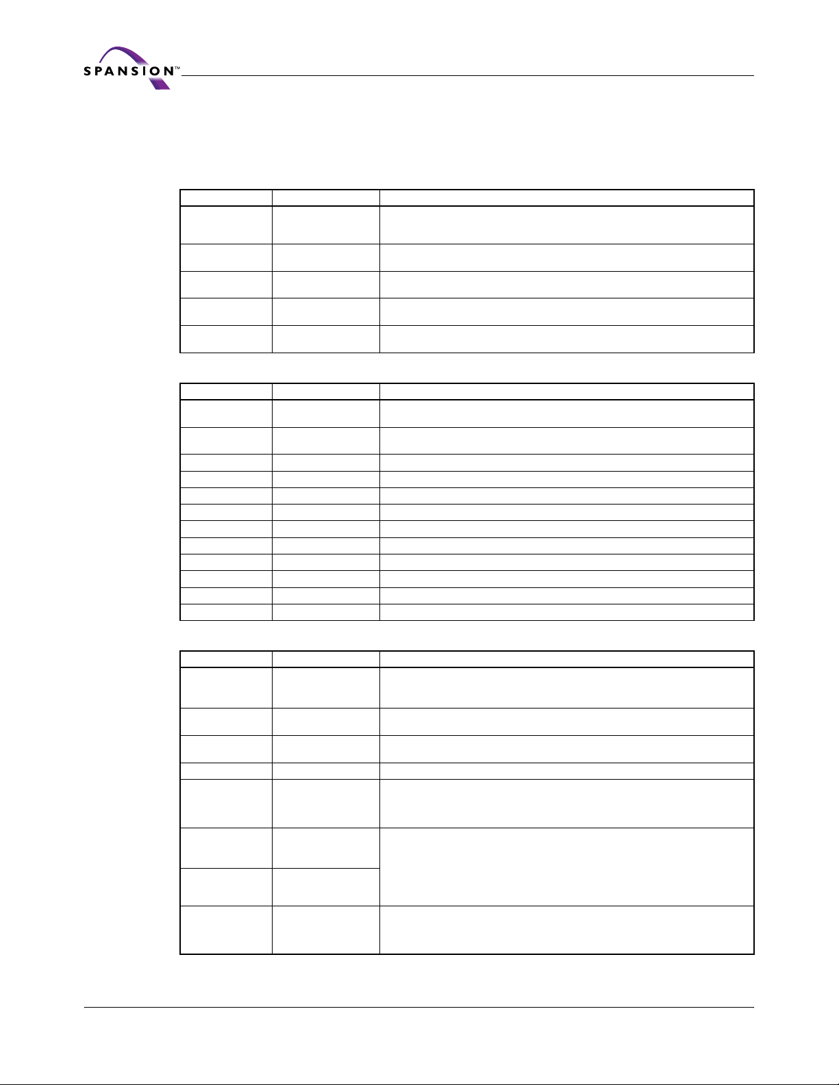
Preliminary
For further information, please see the CFI Specification (see JEDEC publications JEP137-A and
JESD68.01and CFI Publication 100). Please contact your sales office for copies of these
documents.
Table 12.3 CFI Query Identification String
Addresses Data Description
10h
11h
12h
13h
14h
15h
16h
17h
18h
19h
1Ah
0051h
0052h
0059h
0002h
0000h
0040h
0000h
0000h
0000h
0000h
0000h
Query Unique ASCII string QRY
Primary OEM Command Set
Address for Primary Extended Table
Alternate OEM Command Set (00h = none exists)
Address for Alternate OEM Extended Table (00h = none exists)
Table 12.4 System Interface String
Addresses Data Description
V
Min. (write/erase)
1Bh 0027h
1Ch 0036h
1Dh 0000h V
1Eh 0000h V
1Fh 0006h Typical timeout per single byte/word write 2
20h 0009h Typical timeout for Min. size buffer write 2
21h 000Bh Typical timeout per individual block erase 2
22h 0000h Typical timeout for full chip erase 2
23h 0003h Max. timeout for byte/word write 2
24h 0003h Max. timeout for buffer write 2
25h 0002h Max. timeout per individual block erase 2
26h 0000h Max. timeout for full chip erase 2
CC
D7 – D4: volt, D3 – D0: 100 millivolt
V
Max. (write/erase)
CC
D7 – D4: volt, D3 – D0: 100 millivolt
Min. voltage (00h = no VPP pin present)
PP
Max. voltage (00h = no VPP pin present)
PP
N
N
N
times typical
N
times typical (00h = not supported)
N
µs
N
µs (00h = not supported)
N
ms
ms (00h = not supported)
times typical
N
times typical
Table 12.5 Device Geometry Definition
Addresses Data Description
27h
0019h (PL256N)
0018h (PL127N)
Device Size = 2
N
byte
0018h (PL129N)
28h
29h
2Ah
2Bh
0001h
0000h
0006h
0000h
Flash Device Interface description (see CFI publication 100)
Max. number of byte in multi-byte write = 2
(00h = not supported)
N
2Ch 0003h Number of Erase Block Regions within device
2Dh
2Eh
2Fh
30h
0003h
0000h
0000h
0001h
Erase Block Region 1 Information
(see the CFI specification or CFI publication 100)
007Dh (PL256N)
31h
32h
33h
34h
35h
36h
37h
38h
003Dh (PL127N)
003Dh (PL129N)
0000h
0000h
0004h
0003h
0000h
0000h
0001h
Erase Block Region 2 Information
(see the CFI specification or CFI publication 100)
Erase Block Region 3 Information
(see the CFI specification or CFI publication 100)
76 S29PL-N MirrorBit™ Flash Family S29PL-N_00_A4 November 23, 2005
Page 79
Preliminary
Table 12.6 Primary Vendor-Specific Extended Query
Addresses Data Description
40h
41h
42h
43h 0031h Major version number, ASCII (reflects modifications to the silicon)
44h 0034h Minor version number, ASCII (reflects modifications to the CFI table)
45h 0010h
46h 0002h
47h 0001h
48h 0000h
49h 0008h (PL-N)
4Ah
4Bh 0000h
4Ch 0002h (PL-N)
4Dh 0085h
4Eh 0095h
4Fh 0001h
50h 0001h
51h 0001h
52h 0007h Secured Silicon Sector (Customer OTP Area) Size 2
53h 000Fh
54h 000Eh
55h 0005h Erase Suspend Time-out Maximum 2
56h 0005h Program Suspend Time-out Maximum 2
57h 0004h
58h
59h
5Ah
5Bh
0050h
0052h
0049h
0073h (PL256N)
003Bh (PL127N)
003Bh (PL129N)
0013h (PL256N)
000Bh (PL127N)
000Bh (PL129N)
0030h (PL256N)
0018h (PL127N)
0018h (PL129N)
0030h (PL256N)
0018h (PL127N)
0018h (PL129N)
0013h (PL256N)
000Bh (PL127N)
000Bh (PL129N)
Query-unique ASCII string PRI
Address Sensitive Unlock (Bits 1 – 0)
0 = Required, 1 = Not Required
Silicon Technology (Bits 5 – 2) 0100 = 0.11 µm
Erase Suspend
0 = Not Supported, 1 = To Read Only, 2 = To Read & Write
Sector Protect
0 = Not Supported, X = Number of sectors in per group
Sector Temporary Unprotect
00 = Not Supported, 01 = Supported
Sector Protect/Unprotect scheme
01 =29F040 mode, 02 = 29F016 mode, 03 = 29F400 mode,
04 = 29LV800 mode 07 = New Sector Protect mode,
08 = Advanced Sector Protection
Simultaneous Operation
00 = Not Supported, X = Number of Sectors except Bank A
Burst Mode Type
00 = Not Supported, 01 = Supported
Page Mode Type
00 = Not Supported, 01 = 4 Word Page, 02 = 8 Word Page
ACC (Acceleration) Supply Minimum
00h = Not Supported, D7 – D4: Volt, D3 – D0: 100 mV
ACC (Acceleration) Supply Maximum
00h = Not Supported, D7 – D4: Volt, D3 – D0: 100 mV
Top/Bottom Boot Sector Flag
00h = No Boot, 01h = Dual Boot Device, 02h = Bottom Boot Device, 03h = T op
Boot Device
Program Suspend
0 = Not supported, 1 = Supported
Unlock Bypass
00 = Not Supported, 01=Supported
N
bytes
Hardware Reset Low Time-out during an embedded algorithm to read mode
Maximum 2
Hardware Reset Low Time-out not during an embedded algorithm to read mode
Maximum 2
N
ns
N
ns
N
µs
N
µs
Bank Organization
00 = Data at 4Ah is zero, X = Number of Banks
Bank A Region Information. X = Number of sectors in bank
Bank 1 Region Information. X = Number of sectors in bank
Bank 2 Region Information. X = Number of sectors in bank
Bank 3 Region Information. X = Number of sectors in bank
November 23, 2005 S29PL-N_00_A4 S29PL-N MirrorBit™ Flash Family 77
Page 80

13 Commonly Used Terms
Term Definition
Preliminary
ACCelerate.
ACC
A
max
A
min
Asynchronous
Autoselect
Bank
Boot sector
Boundary Location at the beginning or end of series of memory locations.
Burst Read See synchronous read.
Byte 8 bits
CFI
erase operation when raised to a specified voltage above V
may protect all sectors when at a low vo ltage.
Most significant bit of the address input [A23 for 256 Mbit, A22 for 128 Mbit, A21 for
64 Mbit]
Least significant bit of the address input signals (A0 for all devices in this document).
Operation where signal relationships a re based only on propagation delays and are
unrelated to synchronous control (clock) signal.
Read mode for obtaining ma nufacturer and device information as well as sector
protection status.
Section of the memory array consisting of mult iple consecutive sectors. A read
operation in one bank, can be independent of a program or erase operation in a
different bank for devices that offer simultaneous read and write feature.
Smaller size sectors located at the top and or bottom of Flash device address space.
The smaller sector size allows for finer granularity control of erase and protection for
code or parameters used to initiate system operation after p ower on or reset.
Common Flash Interface. A Flash memory i ndustry standard specification [JEDE C 137A and JESD68.01] designed to allow a system to interro gate the Flash to determin e its
size, type and other performance parameters.
A special purpose input signal which allows for faster programming or
. In some devices ACC
CC
Clear Zero (Logic Low Level)
Configuration Register
Continuous Read
Erase Returns bits of a Flash memo ry array to their default state of a lo gical One (High Level).
Erase Suspend/Erase Resume
BGA
Linear Read
MCP
Memory Array The programmable area of th e product available for data storage.
MirrorBit™ Technology
Page
Special purpose register which must be programmed to enable synchronous read
mode
Synchronous method of burst read whereby the device reads continuously until it is
stopped by the host, or it has reached the hig hest address of the memo ry arr ay, after
which the read address wraps around to the lowest memory array address
Halts an erase operation to allow reading or programming in any sector that is not
selected for erasure
Ball Grid Array package. Spansion LLC offers two variations: Fortified Ball Grid Array
and Fine-pitch Ball Grid Array . See th e specific package drawing or connection diagr am
for further details.
Synchronous (burs t) read operation in wh ich 8, 16, or 32 words of sequential data with
or without wraparound before requiring a new initial address
Multi-Chip Product. A method of combining integrated circuits in a single package by
stacking multiple die of the same or different devices.
Spansion™ trademarked techn olo gy for storing multiple bits of data in the same
transistor.
Group of words that may be accessed more rapidly as a group than if the words were
accessed individually.
.
78 S29PL-N MirrorBit™ Flash Family S29PL-N_00_A4 November 23, 2005
Page 81

Preliminary
Term Definition
Asynchronous read operation of several words in which the first word of the group
Page Read
takes a longer initial access time and subsequent words in the group take less page
access time to be read. Different words in the group are accessed by changing only the
least significant address lines.
Password Protection
Persistent Protection
Program
Program Suspend/Program
Resume
Read Host bus cycle that causes the Flash to output data onto the data bus.
Registers
Secured Silicon
Sector Protection
Sector
Sector protection method which uses a programmable password, in addition to the
Persistent Protection method, for protection of sectors in the Flash memory device
Sector protection method that uses commands and only the standard core voltage
supply to control protection of sectors in the Flash memory device. This method
replaces a prior technique of requiring a 12V supply to co ntrol the protectio n me thod .
Stores data into a Flash memory by selectively clearing bits of the memory a rray to
leave a data pattern of ones and zeros.
Halts a programming op er ation to read d ata from an y locat ion that is not selected fo r
programming or erase.
Dynamic storage bits for holding device control information or tracking the status of
an operation.
An area consisting of 256 bytes in which any word may be programmed once, and the
entire area may be protected on ce fr om an y fu tur e pro gramming. Information in this
area may be programmed at the factory or by the user. Once programmed and
protected there is no way to change the secured information. This area is often used
to store a software readable identification such as a serial number.
Use of one or more control bits per sector to indicate whether each sector may be
programmed or erased. If the Protection bit for a sector is set the embedded
algorithms for program or er ase ignore the program or erase commands related to that
sector.
An Area of the memory array in which all bits must be erased together by an erase
operation.
.
Mode of operation in which a host system ma y issue a progr am or er ase com mand to
one bank, that embedded algorithm operation may then proceed while the host
Simultaneous Operation
Synchronous Operation
VersatileIO™ (V
Unlock Bypass
Word
IO
)
immediately follows the embedded algorithm comman d w ith reading from another
Reading may continue concurrently in any bank other than the one executing
bank.
the embedded algorithm operation.
Operation that progresses only when a timing signal, known as a clock, transitions
between logic levels (that is, at a clock edge).
Separate power supply or vo ltage reference signal that allows the host system to set
the voltage levels that the device generates at its data outputs and the voltages
tolerated at its data inputs.
Mode that facilitates faster program times by reducing the number of command bus
cycles required to issue a write operation com mand. In this mode the initial two Unlock
write cycles, of the usual 4 cycle Program command, are not required – reducing all
Program commands to two bus cycles while in this mode.
T wo contiguous bytes (16 bits) located at an even byte boundary. A double word is two
contiguous words located on a two word boundary. A quad word is four contiguous
words located on a four word boundary.
November 23, 2005 S29PL-N_00_A4 S29PL-N MirrorBit™ Flash Family 79
Page 82

Term Definition
Special burst read mode where the read address wraps or returns back to the lowest
Wraparound
Write
Write Buffer
Write Buffer Programming
address boundary in the selected range of words, after read ing the la st Byte o r Word
in the range, e.g. for a 4 word range of 0 to 3, a read beg inning at word 2 would read
words in the sequ ence 2, 3, 0, 1.
Interchangeable term for a program/erase operation where the content of a register
and or memory location is being altered. Th e term write is often associated with writing
command cycles to enter or exit a particular mode of operation.
Multi-word area in which multi ple words may be progr ammed as a sin gle opera tion
Write Buffer may be 16 to 32 w ord s long an d is located on a 16 or 32 word boundary
respectively.
Method of writing multiple words, up to the maximu m siz e of the Write Buffer , in on e
operation. Using Write Buffer Programming results in greater than eight times faster
programming time than by using single word at a time programming commands.
Preliminary
.
A
Write Operation Stat us
Allows the host system to determine the status of a program or erase operation by
reading several special purpose register bits
.
80 S29PL-N MirrorBit™ Flash Family S29PL-N_00_A4 November 23, 2005
Page 83

Preliminary
November 23, 2005 S29PL-N_00_A4 S29PL-N MirrorBit™ Flash Family 81
Page 84

14 Revisions
Revision A0 (February 28, 2005)
Initial Release
Revision A1 (August 8, 2005)
Performance Characteristics
Updated Package Options
MCP Look-Ahead Connection Diagram
Corrected Pinout
Memory Map
Added Sector and Memory Address Map for S29PL127N
Device Operation Table
Added Dual Chip Enable Device Operation Table
VCC Power Up
Updated t
Added VCC ramp rate restriction
VCS
Preliminary
.
DC Characteristics
Updated typical and maximum values.
Revision A2 (October 25, 2005)
Ordering Information
Updated table.
Connection Diagram and Package Dimensions - S29PL-N Fortified BGA
Added pinout and package dimensions.
Global
Changed data sheet status from Advance Information to Preliminary.
Removed Byte Address Information
Distinctive and Performance Characteristics
Removed Enhanced VersatileI/O, updated read access times, and Package options.
Logic Symbol and Block Diagram
Removed VIO from Logic Symbol and Block Diagram .
Erase and Programming Performance
Updated table.
Write Buffer Programming
Updated Write Buffer Abort Description.
Operating Ranges
Updated VIO supply voltages.
DC characteristics
Updated I
CC1
, I
CC4
, I
CC6
.
82 S29PL-N MirrorBit™ Flash Family S29PL-N_00_A4 November 23, 2005
Page 85

Preliminary
Revision A3 (November 14, 2005)
Ordering Information
Updated table
Valid Combinations Table
Updated table
Revision A4 (November 23, 2005)
Logic Symbols
Removed VIO from the illustrations
Block Diagram
Removed VIO from the illustration
Connection Diagrams
Modified Fortified BGA Pinout (LAA064)
PL129N Sector and Memory Address Map
Updated Address Ranges for Banks 2A and 2B
Colophon
The products described in this document are designed, developed and manufactured as contemplated for general use, including without limitation, ordinary
industrial use, general office use, personal use, and household use, but are not designed, developed and manufactured as contemplated (1) for any use that
includes fatal risks or dangers that, unless extremely high safety is secured, could have a serious effect to the public, and could lead directly to death, personal
injury, severe physical damage or other loss (i.e., nuclear reaction control in nuclear facility, aircraft flight control, air traffic control, mass transport control,
medical life support system, missile launch control in weapon system), or (2) for any use where chance of failure is intolerable (i.e., submersible repeater and
artificial satellite). Please note that Spansion will not be liable to you and/or any third party for any claims or damages arising in connection with abovementioned uses of the products. Any semiconductor device has an inherent chance of failure. You must protect against injury, damage or loss from such
failures by incorporating safety design measures into your facility and equipment such as redundancy, fire protection, and prevention of over-current levels
and other abnormal operating conditions. If any products described in this document represent goods or technologies subject to certain restrictions on export under the Foreign Exchange and Foreign Trade Law of Japan, the US Export Administration Regulations or the applicable laws of any other country, the
prior authorization by the respective government entity will be required for export of those products.
Trademarks and Notice
The contents of this document are subject to change without notice. This document may contain information on a Spansion LLC product under development
by Spansion LLC. Spansion LLC reserves the right to change or discontinue work on any product without notice. The information in this document is provided
as is without warranty or guarantee of any kind as to its accuracy, completeness, operability, fitness for particular purpose, merchantability, non-infringement
of third-party rights, or any other warranty, express, implied, or statutory. Spansion LLC assumes no liability for any damages of any kind arising out of the
use of the information in this document.
Copyright ©2005 Spansion LLC. All rights reserved. Spansion, the Spansion logo, and MirrorBit are trademarks of Spansion LLC. Other company and product
names used in this publication are for identification purposes only and may be trademarks of their respective companies.
November 23, 2005 S29PL-N_00_A4 S29PL-N MirrorBit™ Flash Family 83
 Loading...