

Page 1
PRELIMINARY
29F0408
32 Megabit (4M x 8-Bit)
Flash Memory
FEATURES:
• Single 5.0 V supply
• Excellent Single Event Effect
· - SEL
· - SEUTH: = 37 MeV/mg/cm
• Organization:
• Automatic program and erase
• 528-Byte page read operation
• Fast write cycle time
• Command/address/data multiplexed I/O port
• Hardware data protection
• Reliable CMOS floating-gate technology
• Command register operation
• 44 pin flat package
: > 60 MeV/mg/cm
TH
- SEU saturated cross section: 2E-6 cm2/bit
- Memory cell array: (4M + 128k) bit x 8bit
- Data register: (512 + 16) bit x 8bit
- Page program: (512 + 16) Byte
- Block erase: (8K + 256) Byte
- Status register
- Random access: 10 µs (max)
- Serial page access: 50 ns (min)
- Program time: 250 µs (typ)
- Block erase time: 2 ms (typ)
- Program/erase lockout during power transitions
- Endurance: 1,000,000 program/erase cycles
- Data retention: 10 years
2
2
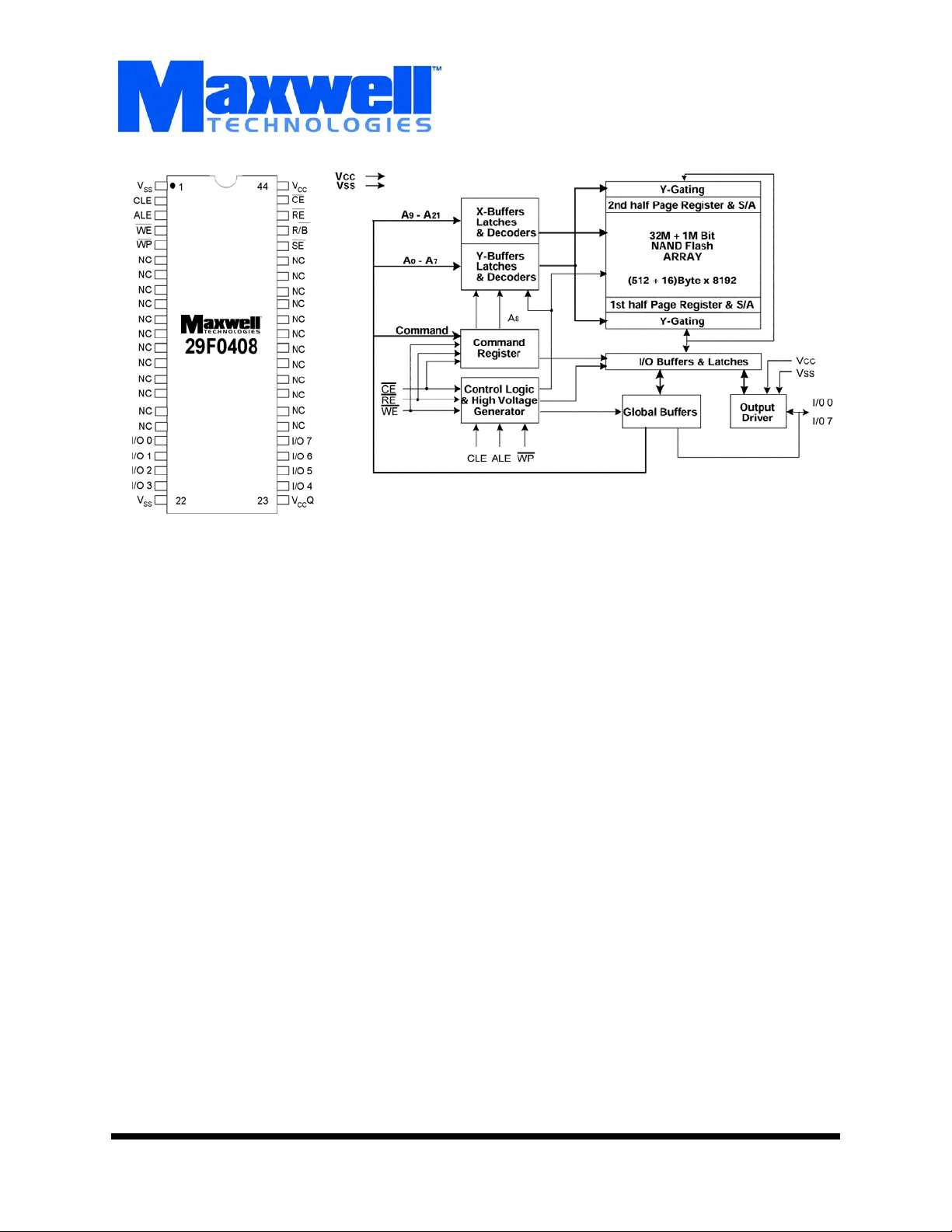
Logic Diagram
DESCRIPTION:
Maxwell Technologies’ 29F0408 high-performance flash memory. The 29F0408 is a 4M (4,194,304) x 8-bit NAND Flash
Memory with a spare 128K (131,072) x 8-bit. A program operation programs the 528-byte page in 250 µs and an erase
operation can be performed in 2 ms on an 8K-byte block. Data
within a page can be read out at 50 ns cycle time per byte.
The on-chip write controller automates all program and erase
functions, including pulse repetition, where required, and internal verify and margining of data. Even write-intensive systems
can take advantage of the 29F0408’s extended reliability of
1,000,000 program/erase cycles by providing either ECC
(Error Correction Code) or real time mapping-out algorithm.
These algorithms have been implemented in many mass storage applications. The spare 16 bytes of a page combined with
the other 512 bytes can be utilized by system-level ECC. The
29F0408 is an optimum solution for large non-volatile storage
applications such as solid state storage, digital voice recorder,
digital still camera and other portable applications requiring
nonvolatility.
Maxwell Technologies' patented R
ogy incorporates radiation shielding in the microcircuit package. Capable of surviving in space environments, the
29F0408 is ideal for satellite, spacecraft, and space probe
missions. It is available with packaging and screening up to
Class S.
AD-PAK® packaging technol-
Memory
1000571
(858) 503-3300 - Fax: (858) 503-3301 - www.maxwell.com
12.19.01 Rev 2
All data sheets are subject to change without notice
©2001 Maxwell Technologies
All rights reserved.
1
Page 2
32 Megabit (4M x 8-Bit) Flash Memory
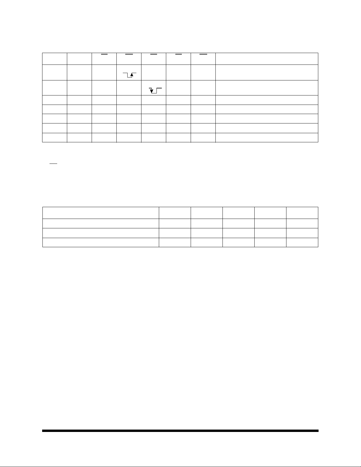
TABLE 1. PINOUT DESCRIPTION
PRELIMINARY
PIN SYMBOL DESCRIPTION
29F0408
2 Command Latch
Enable (CLE)
3 Address Latch Enable
(ALE)
43 Chip Enable (CE
4 Write Enable (WE
42 Read Enable (RE
40 Spare Area Enable
(SE)
18-21,
24-27
5 Write Protect (WP
41 Read/Busy (R/B
I/O Port: I/O0 ~ I/O7 The I/O pins are used to input command, address and data, and to output data during read
The CLE input controls the path activation for commands sent to the command register.
When active high, commands are latched into the command register through the I/O ports
on the rising edge of the WE
The ALE input controls the path activation for address and input data to the internal
address/data register. Addresses are latched on the rising edge or WE
input data is latched when ALE is low.
) The CE input is the device selection control. When CE goes high during a read operation,
the device is returned to standby mode. However, when the device is in the busy state during program or erase, CE
) The WE input controls writes to the I/O port. Commands, address and data are latched on
the rising edge of the WE
) The RE inputs is the serial data-out control, and when active drives the data onto the I/O
bus. Data is valid t
address counter by one.
The SE input controls the spare area selection when SE is high, the device is deselected
the spare area during Read1, Sequential data input and page Program.
operations. The I/O pins float to High-Z when the chip is deselected or when the outputs are
disabled.
) The WP pin provides inadvertent write/erase protection during power transitions. The inter-
nal high voltage generator is reset when the WP
) The R/B output indicates the status of the device operation. When low, it indicates that a
program, erase or random read operation is in process and returns to high state upon completion. It is an open drain output and does not float to High-Z condition when the chip is
deselected or when outputs are disabled.
REA
signal.
with ALE high, and
high is ignored, and does not return the device to standby mode.
pulse.
after the falling edge of RE which also increments the internal column
pin is active low.
6-17, 28-39 NC Not Connected
1, 22 V
44 V
23 V
1000571
SS
CC
Q Output Buffer Voltage
CC
Ground
Supply Voltage
12.19.01 Rev 2
All data sheets are subject to change without notice
©2001 Maxwell Technologies
All rights reserved.
2
Page 3
32 Megabit (4M x 8-Bit) Flash Memory
29F0408
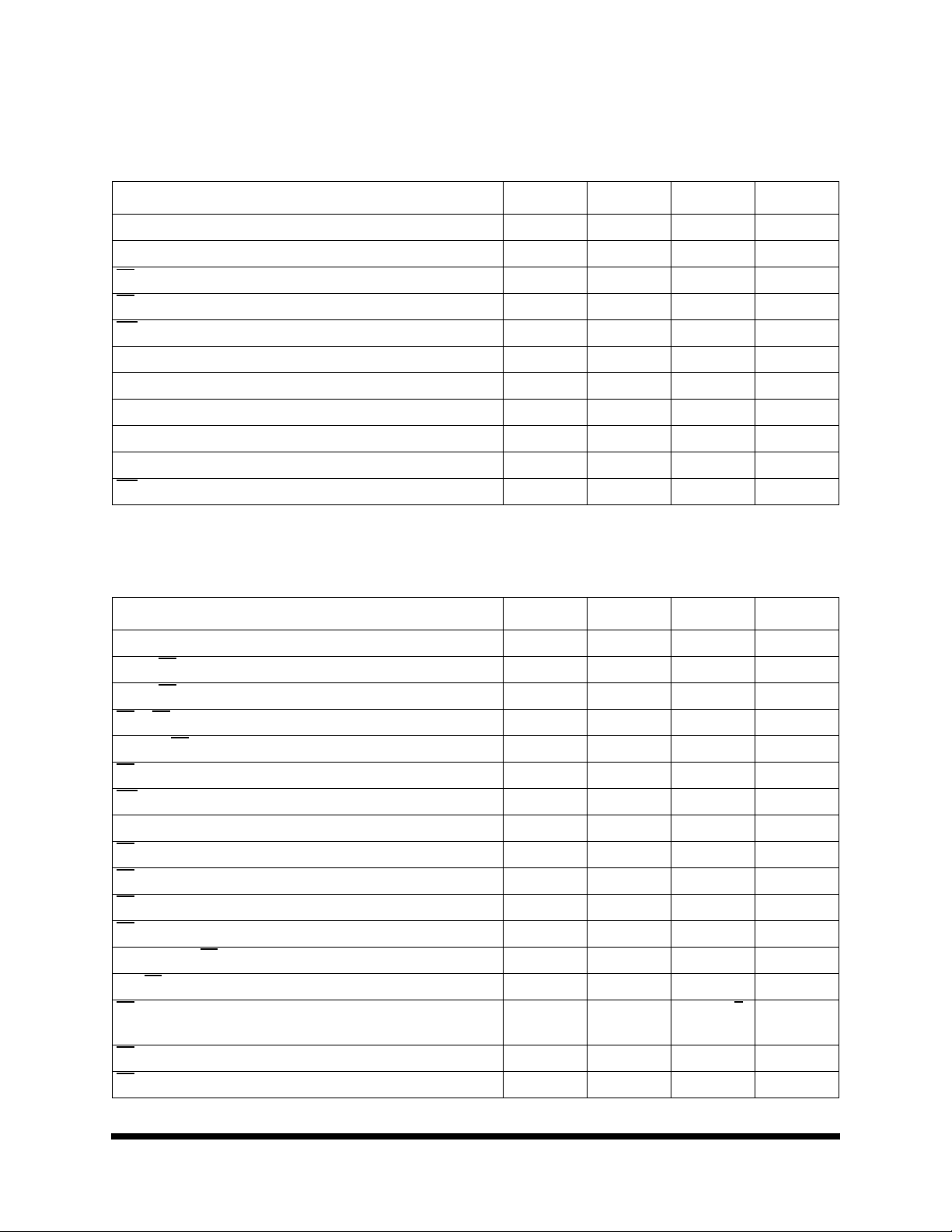
TABLE 2. 29F0408 ABSOLUTE MAXIMUM RATINGS
P
PRELIMINARY
Voltage on any pin relative to V
Temperature under bias T
Storage temperature T
Short circuit output current I
ARAMETER SYMBOL MIN MAX UNIT
SS
V
BIAS
STG
OS
IN
1,2
-0.6 7.0 V
-40 125
-65 150
-- 5 mA
1. Minimum DC voltage is -0.3 V on input/output pins. During transitions, this level may undershoot to -2.0 V for periods < 30 ns.
Maximum DC voltage on input/output pins is V
+ 0.3 V which, during transitions, may overshoot to VCC + 2.0 V for periods <
CC
20 ns.
2. Permanent device damage may occur if ABSOLUTE MAXIMUM RATINGS are exceeded. Functional operation should be
restricted to the conditions as detailed in the operational sections of this data sheet. Exposure to absolute maximum ratings
conditions for extended periods may affect reliability.
TABLE 3. 29F0408 RECOMMENDED OPERATING CONDITIONS
(VOLTAGE REFERENCE TO GND, TA = -40 TO 85°C)
P
ARAMETER SYMBOL MIN TYP MAX UNIT
Supply voltage V
Supply voltage V
Input High Voltage V
Input Low Voltage V
CC
SS
IH
IL
4.5 5.0 5.5 V
000V
2.4 -- VCC ±0.5 V
-0.3 -- 0.8 V
°
C
°
C
TABLE 4. 29F0408 AC TEST CONDITION
(VCC = 5 V ± 10%, TA = -40 TO 85°C, UNLESS OTHERWISE NOTED)
P
ARAMETER MIN MAX UNIT
Input pulse levels 0.4 2.6 V
Input rise times -- 5.0 ns
Input and output timing levels 0.8 2.0 V
1000571
12.19.01 Rev 2
All data sheets are subject to change without notice
©2001 Maxwell Technologies
All rights reserved.
3
Page 4
32 Megabit (4M x 8-Bit) Flash Memory
TABLE 5. 29F0408 DC AND OPERATING CHARACTERISTICS
(VCC = 5 V ± 10%, TA = -40 TO 85°C, UNLESS OTHERWISE NOTED)
PRELIMINARY
P
ARAMETER SYMBOL TEST CONDITIONS MIN TYP MAX UNIT
29F0408
Operating current Sequential read I
Command,
address input
Data input I
Program I
Erase I
Stand-by-current (TTL) I
Stand-by current (CMOS) I
Input leakage current I
Output leakage current I
Input high voltage, all inputs V
Input low voltage, all inputs V
Output high voltage level V
Output low voltage level V
Outuput low current (R/B) I
OL
TABLE 6. 29F0408 CAPACITANCE
t
= 50 ns CE = VIL,
CYCLE
t
CYCLE
CE = VIH, WP = SE = 0V/V
CE = VCC - 0.2, WP = SE = 0V/V
VIN = 0 to 5.5 V -10 -- 10 uA
V
= 0 to 5.5 V -10 -- 10 uA
OUT
IOH = -400 µA 2.4 -- -- V
IOL = 2.1 mA -- -- 0.4 V
I
CC1
CC3
CC4
CC6
CC7
SB1
SB2
LI
LO
IH
IL
OH
OL
I
= 0 mA
OUT
= 50 ns -- 15 30
CC
-- 15 30 mA
-- 15 30
-- 15 30
-- 25 40
-- -- 1 mA
-- 10 100 uA
CC
2.0----V
-- -- 0.8 V
(R/B) VOL = 0.4 V 8 10 -- mA
1
ARAMETER
P
SYMBOL TEST
Input/Output capacitance C
Input capacitance C
C
ONDITION
I/O
IN
VIL = 0V -- 10 pF
VIN = 0V -- 10 pF
MIN MAX UNIT
1. Capacitance is periodically sampled and not 100% tested.
TABLE 7. 29F0408 MODE SELECTION
CLE ALE CE WE RE SE WP MODE
H L L H X X Read Mode Command Input
L H L H X X Address Input (3
Clock)
H L L H X H Write Mode Command Input
L H L H X H Address Input (3
Clock)
1000571
12.19.01 Rev 2
All data sheets are subject to change without notice
©2001 Maxwell Technologies
4
All rights reserved.
Page 5
32 Megabit (4M x 8-Bit) Flash Memory
TABLE 7. 29F0408 MODE SELECTION
CLE ALE CE WE RE SE WP MODE
29F0408
PRELIMINARY
LLL HL/H 1H Data Input
LLLH L/H
LLLHHL/H
XXXXXL/H
XXXXXXHDuring Erase (Busy)
XX
2
XXXXLWrite Protect
XXHXX0V/V
1. When SE is high, spare area is deselected.
2. X can be V
3. WP
should be biased to CMOS high or CMOS low for standby.
or VIH.
IL
TABLE 8. 29F0408 PROGRAM/ERASE CHARACTERISTICS
(VCC = 5 V ± 10%, TA = -40 TO 85°C, UNLESS OTHERWISE NOTED)
P
ARAMETER SYMBOL MIN TYP MAX UNIT
Program time t
Number of partial program cycles in the same page N
Block erase time t
PROG
OP
BERS
CC
1
1
1
X Sequential Read & Data Output
X During Read (Busy)
H During Program (Busy)
3
0V/V
CC
3
Stand-by
-- 0.25 1.5 ms
-- -- 10 cycles
-- 2 10 ms
1000571
12.19.01 Rev 2
All data sheets are subject to change without notice
©2001 Maxwell Technologies
All rights reserved.
5
Page 6
32 Megabit (4M x 8-Bit) Flash Memory
TABLE 9. 29F0408 AC TIMING CHARACTERISTICS FOR COMMAND/ADDRESS/DATA INPUT
(VCC = 5 V ± 10%, TA = -40 TO 85°C, UNLESS OTHERWISE NOTED)
PRELIMINARY
P
ARAMETER SYMBOL MIN MAX UNIT
29F0408
CLE set-up time t
CLE hold time t
CE
setup time t
CE
hold time t
WE
pulse width t
ALE setup time t
ALE hold time t
Data setup time t
Data hold time t
Write cycle time t
WE
high hold time t
TABLE 10. 29F0408 AC CHARACTERISTICS FOR OPERATION
(VCC = 5 V ± 10%, TA = -40 TO 85°C, UNLESS OTHERWISE NOTED)
P
ARAMETER SYMBOL MIN MAX UNIT
Data transfer from cell to register t
ALE to RE
ALE to RE
CE
Ready to RE
RE
WE
Read cycle time t
RE
RE
CE
RE
Output Hi-Z to RE
Last RE
CE
delay (read ID) t
delay (read cycle) t
to RE delay (ID read) t
low t
pulse width t
high to busy t
access time t
high to output Hi-Z t
high to output Hi-Z t
high hold time t
low t
high to busy (at sequential read) t
high to ready (in case of interception by CE at read)
1
t
CLS
CLH
CS
CH
WP
ALS
ALH
DS
DH
WC
WH
R
AR1
AR2
CR
RR
RP
WR
RC
Y
RHZ
CHZ
REH
IR
RB
CRY
0--ns
10 -- ns
0--ns
10 -- ns
25 -- ns
0--ns
10 -- ns
20 -- ns
10 -- ns
50 -- ns
15 -- ns
-- 10 µs
150 -- ns
50 -- ns
100 -- ns
20 -- ns
30 -- ns
-- 100 ns
50 -- ns
-- 35 ns
15 30 ns
-- 20 ns
15 -- ns
0--ns
-- 100 ns
-- 50 + tr (R/B)
2
ns
CE
high hold time (at the last serial read)
RE
low to status output t
1000571
3
12.19.01 Rev 2
t
CEH
RSTO
All data sheets are subject to change without notice
100 -- ns
-- 35 ns
©2001 Maxwell Technologies
All rights reserved.
6
Page 7
32 Megabit (4M x 8-Bit) Flash Memory
TABLE 10. 29F0408 AC CHARACTERISTICS FOR OPERATION
PRELIMINARY
(VCC = 5 V ± 10%, TA = -40 TO 85°C, UNLESS OTHERWISE NOTED)
P
ARAMETER SYMBOL MIN MAX UNIT
29F0408
CE low to status output t
RE
high to WE low t
WE
high to RE low t
Erase suspend input to ready t
RE
access time (read ID) t
Device resetting time (read/program/erase/after erase suspend) t
1. If CE
2. The time to Ready depends on the value of the pull-up resistor tied to R/B
3. To break the sequential read cycle, CE
goes high within 30 ns after the rising edge of the last RE, R/B will not return to VOL.
must be held high for longer than t
Y
Y
WHR
SR
READID
RST
pin.
CEH
.
TABLE 11. 29F0408 VALID BLOCK
P
ARAMETER SYMBOL MIN TYP MAX UNIT
Valid Block Number N
1. The device may include valid blocks. Invalid blocks are defined as blocks that contain one or more bad bits. Do not try to
access these invalid blocks for program and erase. During its lifetime of 10 years and/or 1 million program/erase cycles, the
minimum number of valid blocks are guaranteed though its initial number could be reduced. (Refer to following technical note)
2. The 1st block, which is placed on the 00h block address, is guaranteed to be a valid block.
VB
502 508 512 Blocks
-- 45 ns
0--ns
60 -- ns
-- 500 µs
-- 35 ns
-- 5/10/500/5 µs
1,2
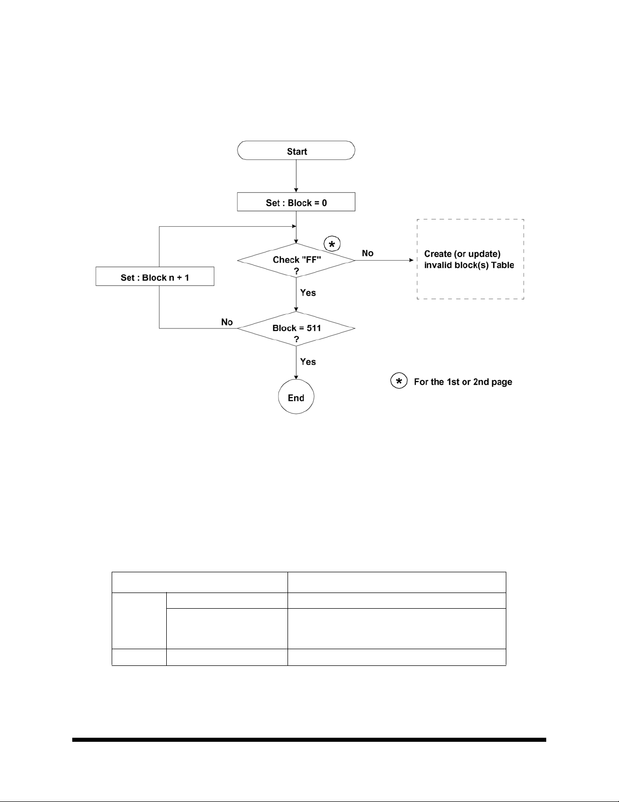
NAND FLASH TECHNICAL NOTES
Invalid Block(s)
Invalid blocks are defined as blocks that contain one or more invalid bits whose reliability is not guaranteed by the
manufacturer. Typically, an invalid block will contain a single bad bit. The information regarding the invalid block(s) is
called as the invalid block information. The invalid block information is written to the 1st or the 2nd page of the invalid
block(s) with 00h data. Devices with invalid block(s) have the same quality level as devices with all valid blocks and
have the same AC and DC characteristics. An invalid block(s) does not affect the performance of valid block(s)
because it is isolated from the bit line and the common source line by a select transistor. The system design must be
able to mask out the invalid block(s) via address mapping. The 1st block of the NAND Flash, however, is fully guaranteed to be a valid block.
Identifying Invalid Block(s)
All device locations are erased (FFh) except locations where the invalid block information is written prior to shipping.
Since the invalid block information is also erasable in most cases, it is impossible to recover the information once it
has been erased. Therefore, the system must be able to recognize the invalid block(s) based on the original invalid
1000571
12.19.01 Rev 2
All data sheets are subject to change without notice
©2001 Maxwell Technologies
All rights reserved.
7
Page 8
32 Megabit (4M x 8-Bit) Flash Memory
block information and create the invalid block table via the following suggested flow chart (Figure 1). Any intentional
erasure of the original block information is prohibited.
29F0408
PRELIMINARY
FIGURE 1. FLOW CHART TO CREATE INVALID BLOCK TABLE
Error in write or read operation
Over its lifetime, the additional invalid blocks may occur. Through the tight process control and intensive testing, additional block failure rate is minimized which is projected below 0.1% until 1 million program/erase cycles. Refer to the
qualification report for the actual data. The following possible failure modes should be considered to implement a
highly reliable system. In the case of status read failure after erase or program, block replacement should be done. To
improve the efficiency of memory space, it is recommended that the read or verification failure due to single bit error
be reclaimed by ECC without any block replacement. The said additional block failure rate does not include those
reclaimed blocks.
FAILURE MODE DETECTION AND COUNTERMEASURE
Write Erase failure Status read after erase Æ Block replacement
Program failure Status read after program
Read Single bit failure Verify ECC
ECC: Error Correcting Code
Example. 1-bit correction and 2-bit detection
1000571
Æ Hamming Code, etc.
Read back (verify after program)
ECC correction
Æ ECC correction
12.19.01 Rev 2
All data sheets are subject to change without notice
Æ Block replacement
Æ Block replacement or
8
©2001 Maxwell Technologies
All rights reserved.
Page 9
32 Megabit (4M x 8-Bit) Flash Memory
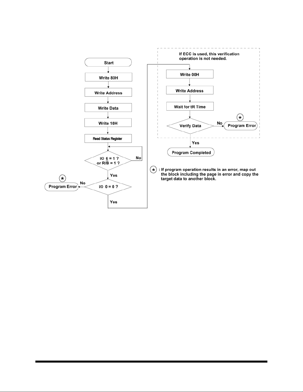
FIGURE 2. PROGRAM FLOW CHART
PRELIMINARY
29F0408
1000571
12.19.01 Rev 2
All data sheets are subject to change without notice
©2001 Maxwell Technologies
All rights reserved.
9
Page 10
32 Megabit (4M x 8-Bit) Flash Memory
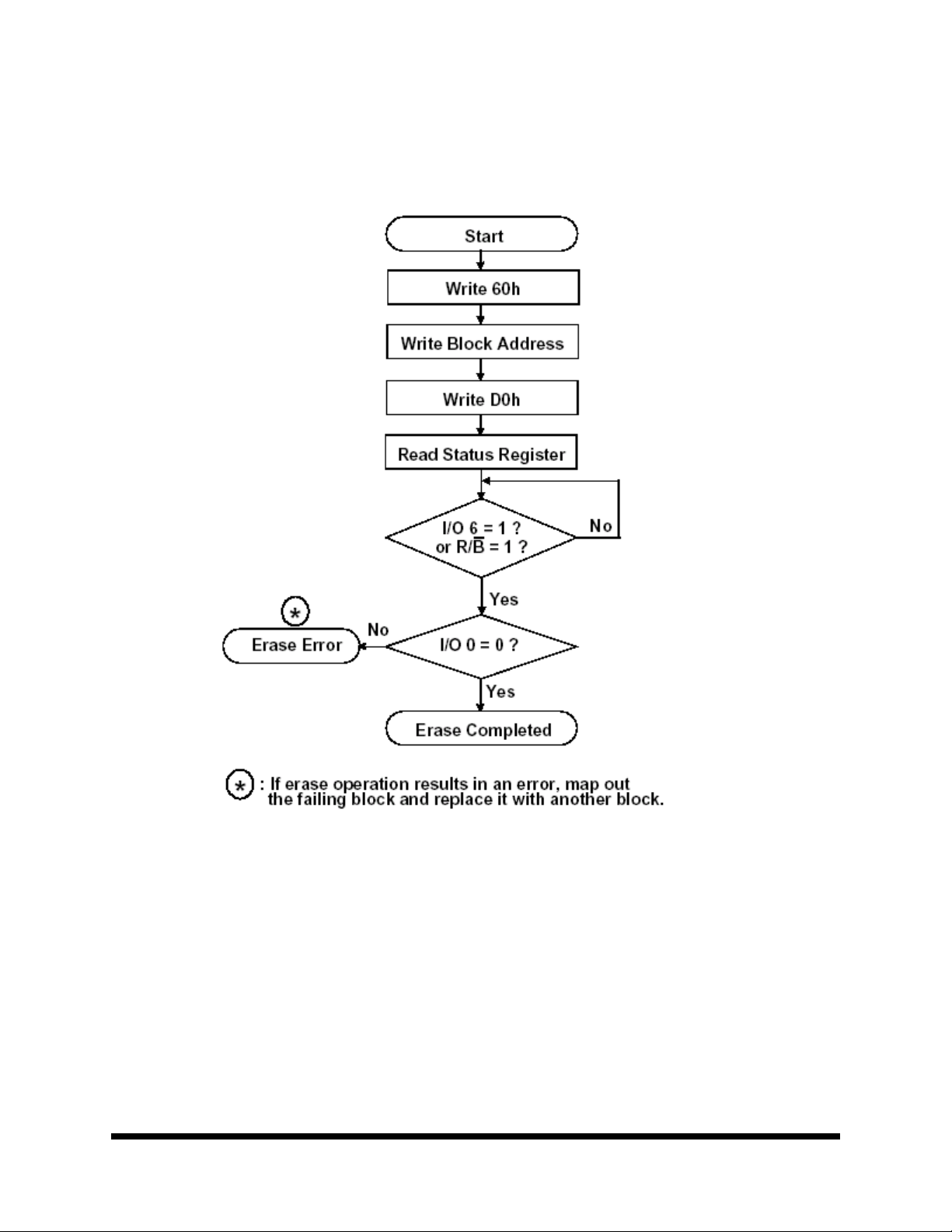
FIGURE 3. ERASE FLOW CHART
PRELIMINARY
29F0408
1000571
12.19.01 Rev 2
All data sheets are subject to change without notice
©2001 Maxwell Technologies
All rights reserved.
10
Page 11

32 Megabit (4M x 8-Bit) Flash Memory
FIGURE 4. READ FLOW CHART
PRELIMINARY
29F0408
1000571
FIGURE 5. BLOCK REPLACEMENT
12.19.01 Rev 2
All data sheets are subject to change without notice
11
©2001 Maxwell Technologies
All rights reserved.
Page 12

32 Megabit (4M x 8-Bit) Flash Memory
Pointer Operation:
The 29F0408 has three modes to set the destination of the pointer. The pointer is set to “A” area by the “00h” com-
PRELIMINARY
mand, to “B” area by the “01h” command, and to “C” area by the “50h” command. The Destination Pointer Table shows
the destination of the pointer, and the block diagram shows the diagram of its operation.
29F0408
TABLE 12. DESTINATION OF POINTER TABLE
FIGURE 6. BLOCK DIAGRAM OF POINTER OPERATION
1000571
12.19.01 Rev 2
All data sheets are subject to change without notice
©2001 Maxwell Technologies
All rights reserved.
12
Page 13

32 Megabit (4M x 8-Bit) Flash Memory
FIGURE 7. EXAMPLES OF PROGRAMMING WITH SUCCESSIVE POINTER OPERATION
PRELIMINARY
TABLE 13. POINT STATUS AFTER EACH OPERATION
29F0408
System Interface Using CE don’t-care.
For a easier system interface, CE may be inactive during the data-loading or sequential data-reading as shown below.
The internal 528byte page registers are utilized as seperate buffers for this operation and the system design gets
more flexible. In addition, for voice or audio applications which use slow cycle time on the order of u-seconds, de-activating CE during the data-loading and reading would provide significant savings in power consumption.
1000571
12.19.01 Rev 2
All data sheets are subject to change without notice
©2001 Maxwell Technologies
All rights reserved.
13
Page 14

32 Megabit (4M x 8-Bit) Flash Memory
FIGURE 8. PROGRAM OPERATION WITH CE DON’T CARE
PRELIMINARY
29F0408
Timing requirements: If CE is is exerted high
during data-loading, tCS must be minimum
10ns and tWC must be increased accordingly.
FIGURE 9. READ OPERATION WITH CE DON’T CARE
Timing requirements: If CE
during sequentialdata-reading, the falling edge
of CE to valid data(tCEA) must be kept greater
than 45ns.
is is exerted high
1000571
12.19.01 Rev 2
All data sheets are subject to change without notice
©2001 Maxwell Technologies
All rights reserved.
14
Page 15

32 Megabit (4M x 8-Bit) Flash Memory
FIGURE 10. COMMAND LATCH CYCLE
PRELIMINARY
29F0408
FIGURE 11. ADDRESS LATCH CYCLE
1000571
12.19.01 Rev 2
All data sheets are subject to change without notice
©2001 Maxwell Technologies
All rights reserved.
15
Page 16

32 Megabit (4M x 8-Bit) Flash Memory
FIGURE 12. INPUT DATA LATCH CYCLE
PRELIMINARY
29F0408
FIGURE 13. SEQUENTIAL OUT CYCLE AFTER READ (CLE = L, WE = H, ALE = L)
1000571
12.19.01 Rev 2
All data sheets are subject to change without notice
©2001 Maxwell Technologies
All rights reserved.
16
Page 17

32 Megabit (4M x 8-Bit) Flash Memory
29F0408
PRELIMINARY
FIGURE 14. STATUS READ CYCLE
FIGURE 15. READ1 OPERATION (READ ONE PAGE)
1000571
12.19.01 Rev 2
All data sheets are subject to change without notice
©2001 Maxwell Technologies
All rights reserved.
17
Page 18

32 Megabit (4M x 8-Bit) Flash Memory
FIGURE 16. READ1 OPERATION (INTERCEPTED BY CE)
PRELIMINARY
29F0408
IGURE 17. READ2 OPERATION (READ ONE PAGE)
F
1000571
12.19.01 Rev 2
All data sheets are subject to change without notice
©2001 Maxwell Technologies
All rights reserved.
18
Page 19

32 Megabit (4M x 8-Bit) Flash Memory
29F0408
PRELIMINARY
FIGURE 18. SEQUENTIAL ROW READ OPERATION
FIGURE 19. PAGE PROGRAM OPERATION
1000571
12.19.01 Rev 2
All data sheets are subject to change without notice
©2001 Maxwell Technologies
All rights reserved.
19
Page 20

32 Megabit (4M x 8-Bit) Flash Memory
FIGURE 20. BLOCK ERASE OPERATION (ERASE ONE BLOCK)
PRELIMINARY
IGURE 21. MANUFACTURE & DEVICE ID READ OPERATION
F
29F0408
1000571
12.19.01 Rev 2
All data sheets are subject to change without notice
©2001 Maxwell Technologies
All rights reserved.
20
Page 21

32 Megabit (4M x 8-Bit) Flash Memory
29F0408
DEVICE OPERATION
PAGE READ
PRELIMINARY
Upon initial device power up, the device defaults to Read1 mode. This operation is also initiated by writing
00h to the command register along with three address cycles. Once the command is latched, it does not
need to be written for the following page read operation. Three types of operations are available : random
read, serial page read and sequential read.
The random read mode is enabled when the page address is changed. The 528 bytes of data within the
selected page are transferred to the data registers in less than 10 ms(tR). The CPU can detect the completion of this data transfer(t
registers, they may be read out in 50 ns cycle time by sequentially pulsing RE
low transitions of the RE
umn address(column 511 or 527 depending on state of SE
After the data of last column address is clocked out, the next page is automatically selected for sequential
read.
) by analyzing the output of R/B pin. Once the data in a page is loaded into the
R
with CE staying low. High to
clock output the data starting from the selected column address up to the last col-
pin).
Waiting 10 µs again allows for reading of the selected page. The sequential read operation is terminated by
bringing CE high. The way the Read1 and Read2 commands work is like a pointer set to either the main
area or the spare area. The spare area of bytes 512 to 527 may be selectively accessed by writing the
Read2 command with SE pin low. Toggling SE
starting address of the spare area while addresses A4 to A7 are ignored. Unless the operation is aborted,
the page address is automatically incremented for sequential read as in Read1 operation and spare sixteen
bytes of each page may be sequentially read. The Read1 command (00h/01h) is needed to move the
pointer back to the main area. Figures 22 thru 25 show typical sequence and timings for each read operation.
during operation is prohibited. Addresses A0 to A3 set the
1000571
12.19.01 Rev 2
All data sheets are subject to change without notice
©2001 Maxwell Technologies
All rights reserved.
21
Page 22

32 Megabit (4M x 8-Bit) Flash Memory
29F0408
PRELIMINARY
FIGURE 22. READ1 OPERATION
1000571
12.19.01 Rev 2
All data sheets are subject to change without notice
©2001 Maxwell Technologies
All rights reserved.
22
Page 23

32 Megabit (4M x 8-Bit) Flash Memory
29F0408
PRELIMINARY
FIGURE 23. READ2 OPERATION
1000571
12.19.01 Rev 2
All data sheets are subject to change without notice
©2001 Maxwell Technologies
All rights reserved.
23
Page 24

32 Megabit (4M x 8-Bit) Flash Memory
29F0408
PRELIMINARY
FIGURE 24. SEQUENTIAL ROW READ1 OPERATION
FIGURE 25. SEQUENTIAL READ2 OPERATION (SE = FIXED LOW)
1000571
12.19.01 Rev 2
All data sheets are subject to change without notice
©2001 Maxwell Technologies
All rights reserved.
24
Page 25

32 Megabit (4M x 8-Bit) Flash Memory
29F0408
PAGE PROGRAM
The device is programmed basically on a page basis, but it does allow multiple partial page programming of
PRELIMINARY
a byte or consecutive bytes up to 528, in a single page program cycle. The number of consecutive partial
page programming operation within the same page without an intervening erase operation must not exceed
ten. The addressing may be done in any random order in a block. A page program cycle consists of a serial
data loading period in which up to 528 bytes of data may be loaded into the page register, followed by a nonvolatile programming period where the loaded data is programmed into the appropriate cell. Serial data
loading can be started from 2nd half array. About the pointer operation, please refer to the attached technical
notes.The serial data loading period begins by inputting the Serial Data Input command (80H), followed by
the three cycle address input and then serial data loading. The bytes other than those to be programmed do
not need to be loaded.
The Page Program confirm command (10h) initiates the programming process. Writing 10h alone without
perviously entering the serial data will not initiate the programming process. The internal write controller
automatically executes the algorithms and timings necessary for program and verify, thereby freeing the
CPU for other tasks. Once the program process starts, the Read Status Register command may be entered,
with RE
monitoring the R/B
and Reset command are valid while programming is in progress. When the Page Program is complete, the
Write Status Bit (I/O0) may be checked (Figure 26). The internal write verify detects only errors for "1"s that
are not successfully programmed to "0"s. The command register remains in Read Status command mode
until another valid command is written to the command register.
and CE low, to read the status register. The CPU can detect the completion of a program cycle by
output, or the Status bit (I/O6) of the Status Register. Only the Read Status command
1000571
FIGURE 26. PROGRAM & READ STATUS OPERATION
12.19.01 Rev 2
All data sheets are subject to change without notice
25
©2001 Maxwell Technologies
All rights reserved.
Page 26

32 Megabit (4M x 8-Bit) Flash Memory
29F0408
BLOCK ERASE
The Erase operation can erase on a block (8K Byte) basis. Block address loading is accomplished in two
PRELIMINARY
cycles initiated by an Erase Setup command (60h). Only address A13 to A21 is valid while A9 to A12 is
ignored. The addresses of the block to be erased to FFh. The Erase Confirm command (D0h) following the
block address loading initiates the internal erasing process. This two-step sequence of setup followed by
execution ensures that memory contents are not accidentally erased due to external noise conditions. At the
rising edge of WE
erase-verify. When the erase operation is completed, the Write Status Bit (I/O0) may be checked. Figure 27
details the sequence.
after the erase confirm command input, the internal write controller handles erase and
FIGURE 27. BLOCK ERASE OPERATION
READ STATUS
The device contains a Status Register which may be read to find out whether program or erase operation is
complete, and whether the program or erase operation completed successfully. After writing 70h command
to the command register, a read cycle outputs the contents of the Status Register to the I/O pins on the falling edge of CE or RE, whichever occurs last. This two line control allows the system to poll the progress of
each device in multiple memory connections even when R/B
need to be toggled for updated status. Refer to table 14 for specific Status Register definitions. The command register remains in Status Read mode until further commands are issued to it. Therefore, if the status
register is read during a random read cycle, a read command (00h or 50h) should be given before sequential
page read cycle.
1000571
12.19.01 Rev 2
pins are common-wired. RE or CE does not
All data sheets are subject to change without notice
26
©2001 Maxwell Technologies
All rights reserved.
Page 27

32 Megabit (4M x 8-Bit) Flash Memory
29F0408
PRELIMINARY
TABLE 14. READ STATUS REGISTER DEFINITION
READ ID
The device contains a product identification mode, initiated by writing 90h to the command register, followed
by an address input of 00h. Two read cycles sequentially output the manufacture code(ECh), and the device
code (E3h) respectively. The command register remains in Read ID mode until further commands are issued
to it. Figure 28 shows the operation sequence.
1000571
FIGURE 28. READ ID OPERATION
12.19.01 Rev 2
All data sheets are subject to change without notice
27
©2001 Maxwell Technologies
All rights reserved.
Page 28

32 Megabit (4M x 8-Bit) Flash Memory
29F0408
RESET
The device offers a reset feature, executed by writing FFh to the command register. When the device is in
PRELIMINARY
Busy state during random read, program or erase modes, the reset operation will abort these operation. The
contents of memory cells being altered are no longer valid, as the data will be partially programmed or
erased. Internal address registers are cleared to "0"s and data registers to "1"s. The command register is
cleared to wait for the next command, and the Status Register is cleared to value C0h when WP
Refer to table 15 for device status after reset operation. If the device is already in reset state a new reset
command will not be accepted to by the command register. The R/B
Reset command is written. Reset command is not necessary for normal operation. Refer to Figure 29 below.
pin transitions to low for t
RST
FIGURE 29. RESET OPERATION
is high.
after the
TABLE 15. DEVICE STATUS
DATA PROTECTION
The device is designed to offer protection from any involuntary program/erase during power-transitions. An
internal voltage detector disables all functions whenever V
protection and is recommended to be kept at V
The two step command sequence for program/erase provides additional software protection.
during power-up and power-down as shown in Figure 30.
IL
is below about 2V. WP pin provides hardware
CC
1000571
12.19.01 Rev 2
All data sheets are subject to change without notice
©2001 Maxwell Technologies
All rights reserved.
28
Page 29

32 Megabit (4M x 8-Bit) Flash Memory
29F0408
PRELIMINARY
FIGURE 30. AC WAVEFORMS FOR POWER TRANSITION
READY/BUSY
The device has a R/B output that provides a hardware method of indicating the completion of a page program, erase and random read completion. The R/B
or erase command is written to the command register or random read is begin after address loading. It
returns to high when the internal controller has finished the operation. The pin is an open-drain driver
thereby allowing two or more R/B outputs to be Or-tied. An appropriate pull-up resister is required for proper
operation and the value may be calculated by following equation.
pin is normally high but transitions to low after program
1000571
12.19.01 Rev 2
All data sheets are subject to change without notice
©2001 Maxwell Technologies
All rights reserved.
29
Page 30

32 Megabit (4M x 8-Bit) Flash Memory
29F0408
PRELIMINARY
FIGURE 31. READY/BUSY
1000571
12.19.01 Rev 2
All data sheets are subject to change without notice
©2001 Maxwell Technologies
All rights reserved.
30
Page 31

32 Megabit (4M x 8-Bit) Flash Memory
PRELIMINARY
29F0408
44 PIN RAD-PAK® FLAT PACKAGE
SYMBOL
MIN NOM MAX
A 0.132 0.147 0.160
b 0.015 0.017 0.019
c 0.006 0.008 0.10
D 1.188 1.200 1.212
E 0.668 0.675 0.682
E1 -- -- 0.705
E2 0.450 0.455 0.460
E3 0.098 0.110 0.122
e 0.050 BSC
L 0.350 0.370 0.390
Q 0.022 0.027 0.032
S1 0.005 -- --
N44
F44-01
Note: All dimensions in inches
DIMENSION
1000571
12.19.01 Rev 2
All data sheets are subject to change without notice
©2001 Maxwell Technologies
All rights reserved.
31
Page 32

32 Megabit (4M x 8-Bit) Flash Memory
Important Notice:
These data sheets are created using the chip manufacturer’s published specifications. Maxwell Technologies verifies
PRELIMINARY
functionality by testing key parameters either by 100% testing, sample testing or characterization.
The specifications presented within these data sheets represent the latest and most accurate information available to
date. However, these specifications are subject to change without notice and Maxwell Technologies assumes no
responsibility for the use of this information.
Maxwell Technologies’ products are not authorized for use as critical components in life support devices or systems
without express written approval from Maxwell Technologies.
Any claim against Space Electronics Inc. must be made within 90 days from the date of shipment from Maxwell Technologies. Maxwell Technologies’ liability shall be limited to replacement of defective parts.
29F0408
1000571
12.19.01 Rev 2
All data sheets are subject to change without notice
©2001 Maxwell Technologies
All rights reserved.
32
Page 33

32 Megabit (4M x 8-Bit) Flash Memory
)
Product Ordering Options
29F0408
PRELIMINARY
29F0408
Model Number
RP
F X
Feature
Screening Flow
Package
Option Details
Monolithic
S = Maxwell Class S
B = Maxwell Class B
E = Engineering (testing @ +25°C
I = Industrial (testing @ -55°C,
+25°C, +125°C)
F = Flat Pack
1000571
Radiation Feature
Base Product
Nomenclature
12.19.01 Rev 2
RP = R
AD-PAK® package
32 Megabit (4M x 8-Bit) Flash
Memory
All data sheets are subject to change without notice
33
©2001 Maxwell Technologies
All rights reserved.
 Loading...