

Page 1
FINAL
Am27C010
1 Megabit (128 K x 8-Bit) CMOS EPROM
DISTINCTIVE CHARACTERISTICS
■ Fast acce ss tim e
— Speed options as fast as 45 ns
■ Low power consumption
— 20 µA typical CMOS standby current
■ JEDEC-approved pinout
■ Single +5 V power supply
■ ±10% power supply tolerance standard
GENERAL DESCRIPTION
The Am27 C010 is a 1 Mega bit , ult ra vio let e ras ab le pr ogrammable read-only memory. It is organized as 128K
words by 8 bits per word, operates from a single +5 V
supply, has a static standby mode, and features fast
single addr ess location programming. Pro ducts are
available in windowed ceramic DIP packages, as well
as plastic on e time programma ble (OTP) PDIP and
PLCC packages.
Data can be typically accessed in less than 45 ns, allowing high-performance microprocessors to operate
without any WAIT states. The device offers separate
Output Ena ble ( OE#) and Chip En abl e ( CE #) co ntr ols,
■ 100% Flashrite™ programming
— Typical programming time of 16 seconds
■ Latch-up protected to 100 mA from –1 V to
V
+ 1 V
CC
■ High noise immunity
■ Versatile features for simple interfacing
— Both CMOS and TTL input/output compatibility
— Two line control functions
■ Standard 32-pin DIP, PDIP, and PLCC packages
thus eliminating bus contention in a multiple bus microprocessor system .
AMD’s CMOS process technology provides high
speed, low power, and high noise immunity. Typical
power consumption is only 10 0 mW in acti ve mode,
and 100 µW in standby mode.
All sign als are TTL levels, including programm ing signals. Bit locati ons may be programmed sing ly, in
blocks, or at random. The device suppor ts AMD’s
Flashrite programming algorithm (100 µs pulses), resulting in a typical programming time of 16 seconds.
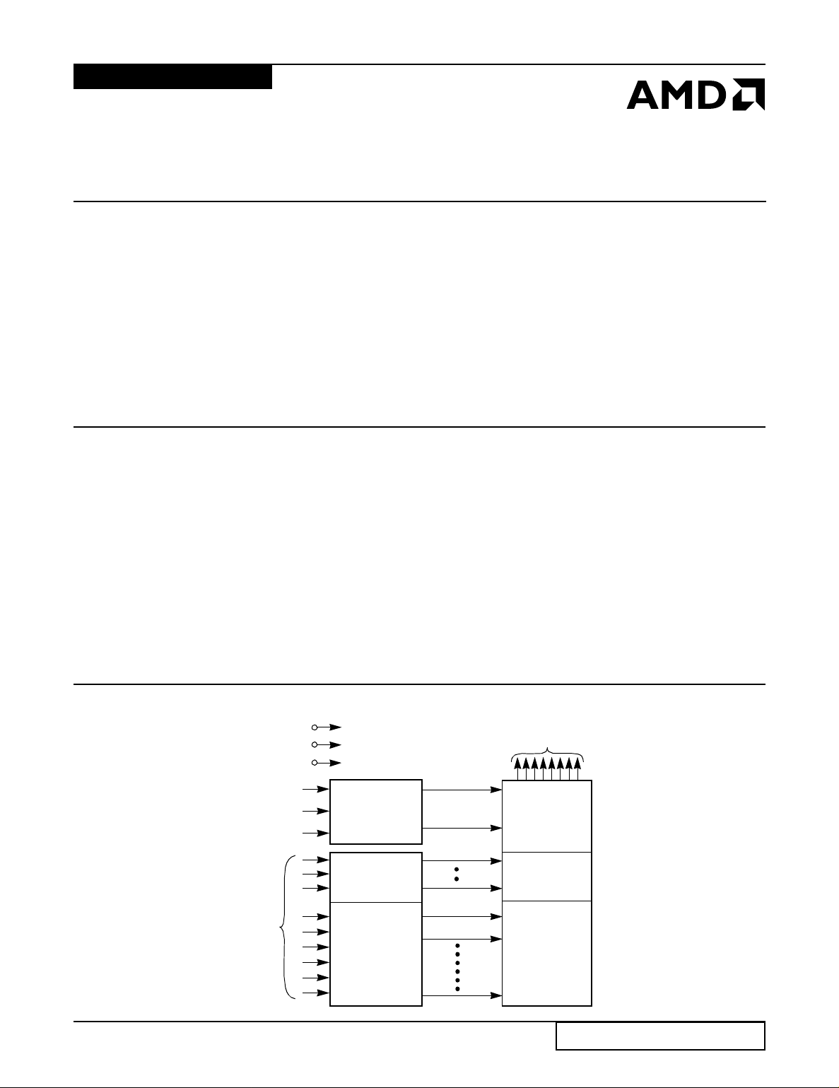
BLOCK DIAGRAM
PGM#
A0–A16
Address
Inputs
OE#
CE#
V
CC
V
SS
V
PP
Output Enable
Chip Enable
and
Prog Logic
Y
Decoder
X
Decoder
Data Outputs
DQ0–DQ7
Output
Buffers
Y
Gating
1,048,576
Bit Cell
Matrix
Publication# 10205 Rev: J Amendment/0
Issu e Date: July 2, 1999
10205J-1
Page 2
PRODUCT SELECTOR GUIDE
Family Part Number Am27C010
V
= 5.0 V ± 5% -45 -255
Speed Options
Max Access Time (ns) 45 55 70 90 120 150 200 250
CE# (E#) Access (ns) 45 55 70 90 120 150 200 250
OE# (G#) Access (ns) 25 35 35 40 50 65 75 75
CC
V
= 5.0 V ± 10% -45 -55 -70 -90 -120 -150 -200
CC
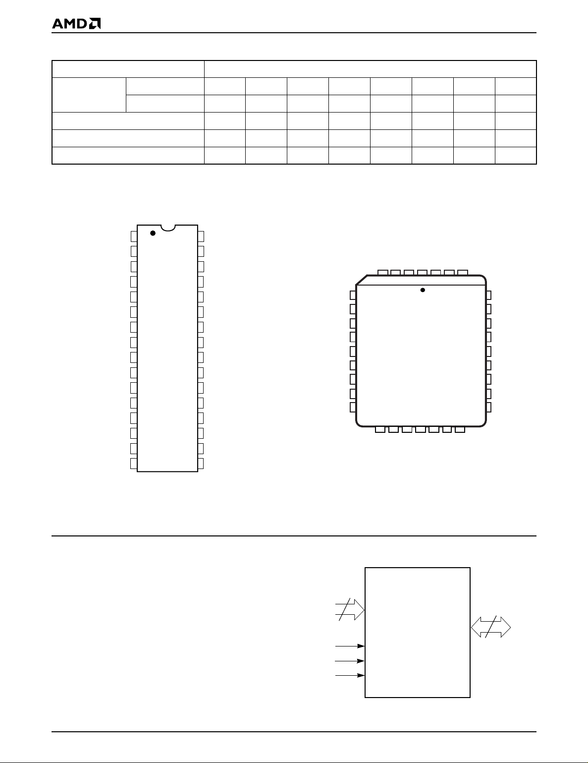
CONNECTION DIAGRAMS
Top View
DIP PLCC
32
31
30
29
28
27
26
25
24
23
22
21
20
19
18
17
V
CC
PGM# (P#)
NC
A14
A13
A8
A9
A11
OE# (G#)
A10
CE# (E#)
DQ7
DQ6
DQ5
DQ4
DQ3
10205J-2
A7
A6
A5
A4
A3
A2
A1
A0
DQ0
5
6
7
8
9
10
11
12
13
14
A12
15
DQ1
A15
DQ2
A16
SS
V
17
PP
V
13130234
18
DQ3
32
DQ4
CC
V
19 2016
PGM# (P#)
NC
29
28
27
26
25
24
23
22
21
DQ6
DQ5
A14
A13
A8
A9
A11
OE# (G#)
A10
CE# (E#)
DQ7
10205J-3
V
PP
A16
A15
A12
A7
A6
A5
A4
A3
A2
A1
A0
DQ0
DQ1
DQ2
V
SS
1
2
3
4
5
6
7
8
9
10
11
12
13
14
15
16
Notes:
1. JEDEC nomenclature is in parenthesis.
2. The 32-pin DIP to 32-pin PLCC configuration varies from the JEDEC 28-pin DIP to 32-pin PLCC configuration.
PIN DESIGNATIONS
LOGIC SYMBOL
A0–A16 = Address Inputs
CE# (E#) = Chip Enable Input
DQ0–DQ7 = Data Input/ Ou tpu ts
OE# (G#) = Output Enable Input
17
A0–A16
8
DQ0–DQ7
PGM# (P#) = Program Enable Input
V
CC
V
PP
V
SS
=VCC Supply Voltage
= Program Voltage Input
=Ground
CE# (E#)
PGM# (P#)
OE# (G#)
10205J-4
2Am27C010
Page 3
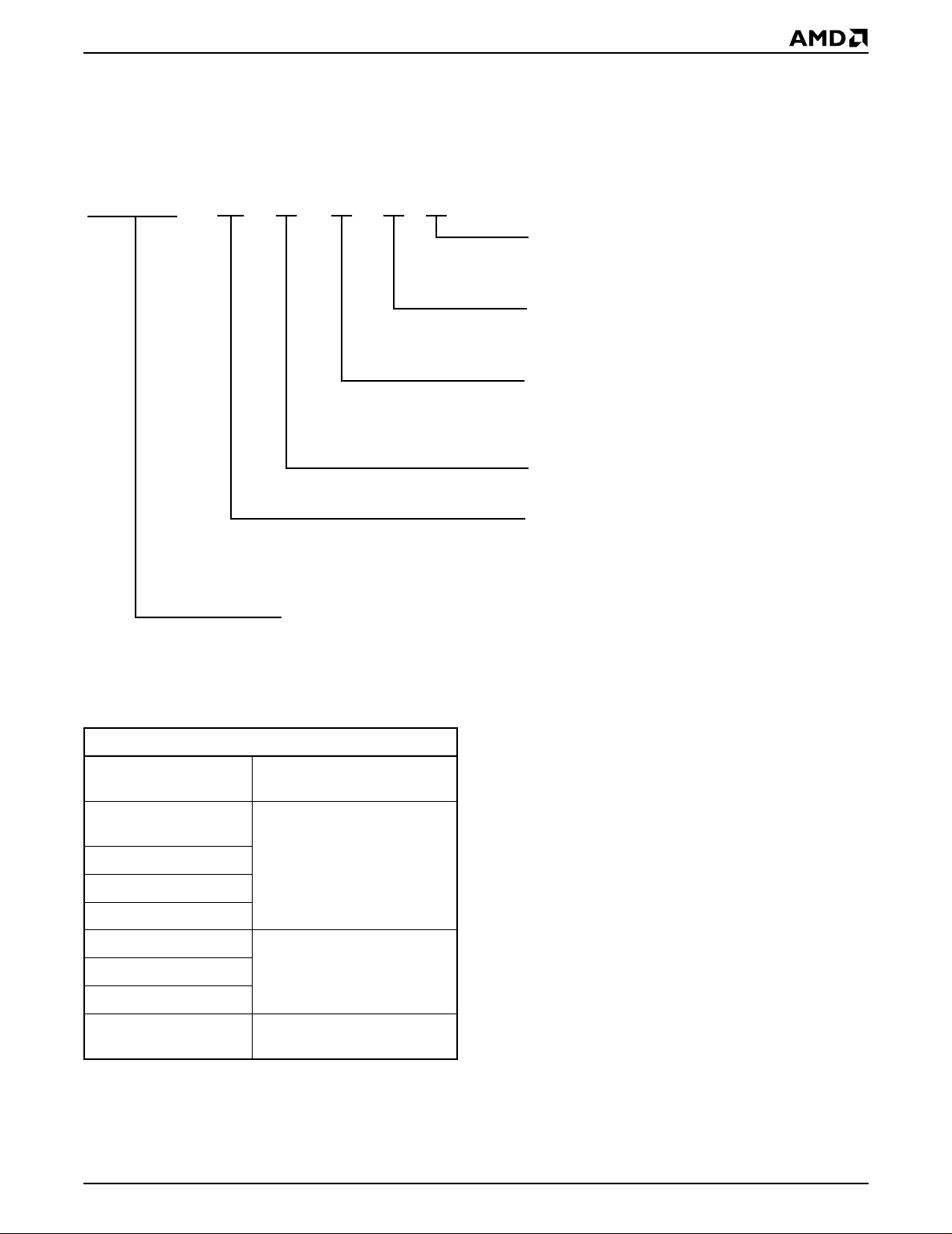
ORDERING INFORMATION
UV EPROM Products
AMD standard products are available in several packages and operating ranges. The order number (V alid Combination) is formed
by a combination of the following:
AM27C010 -45 D C
DEVICE NUMBER/DESCRIPTION
Am27C010
1 Megabit (128 K x 8-Bit) CMOS UV EPROM
5
B
OPTIONAL PROCESSING
Blank = Standard Processing
B = Burn-In
VOLTAGE TOLERANCE
5=V
See Product Selector Guide and Valid Combinations
TEMPERATURE RANGE
C = Commercial (0°C to +70
I=Industrial (–40
E = Extended (–55°C to +125°C)
PACKAGE TYPE
D = 32-Pin Ceramic DIP (CDV032)
SPEED OPTION
See Product Selector Guide and Valid Combinations
± 5%, 45 ns only
CC
°C)
°C to +85°C)
AM27C010-45
V
= 5.0 V ± 5%
CC
AM27C010-45
V
= 5.0 V ± 10%
CC
AM27C010-55
AM27C010-70
AM27C010-90
AM27C010-120
AM27C010-200
AM27C010-255
V
= 5.0 V ± 5%
CC
Valid Combinations
DC5, DC5B, DI5, DI5B
DC, DCB, DI, DIB
DC, DCB, DI, DIB, DE, DEBAM27C010-150
DC, DCB, DI, DIB
Valid Combinations
Valid Combinations list configurations planned to be supported in volume for this device. Consult the local AMD sales
office to confirm availability of specific valid combinations and
to check on newly released combinations.
Am27C010 3
Page 4
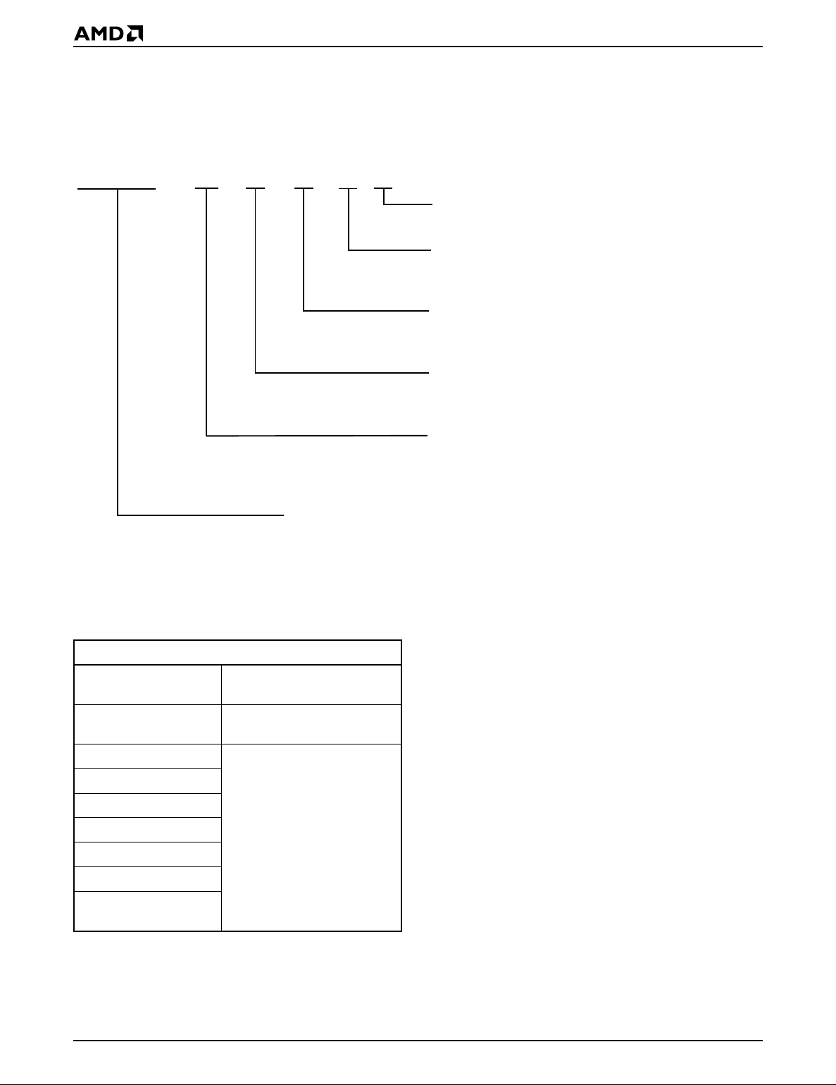
ORDERING INFORMATION
OTP EPROM Pro d u cts
AMD standard products are available in several packages and operating ranges. The order number (V alid Combination) is formed
by a combination of the following:
AM27C010 -45 J C
DEVICE NUMBER/DESCRIPTION
Am27C010
1 Megabit (128 K x 8-Bit) CMOS OTP EPROM
5
OPTIONAL PROCESSING
Blank = Sta ndard Proces sing
VOLTAGE TOLERANCE
5=V
See Product Selector Guide and Valid Combinations
TEMPERATURE RANGE
C = Commercial (0
I=Industrial (–40
PACKAGE TYPE
P = 32-Pin Plastic DIP (PD 032)
J = 32-Pin Plastic Leaded Chip Carrier (PL 032)
SPEED OPTION
See Product Selector Guide and Valid Combinations
± 5%, 45 ns only
CC
°C to +70°C)
°C to +85°C)
Valid Combinations
AM27C010-45
V
= 5.0 V ± 5%
CC
AM27C010-45
V
= 5.0 V ± 10%
CC
AM27C010-55
AM27C010-70
AM27C010-90
AM27C010-120
AM27C010-150
AM27C010-200
AM27C010-255
V
= 5.0 V ± 5%
CC
Valid Combinations
PC5, PI5, JC5, JI5
JC, PC, JI, PI
Valid Combinations list configurations planned to be supported in volume for this device. Consult the local AMD sales
office to confirm availability of specific valid combinations and
to check on newly released combinations.
JC, PC
4Am27C010
Page 5

FUNCTIONAL DESCRIPTION
Device Erasure
In order to clear all locations of their programmed contents, the device must be exposed to an ultraviolet light
source. A dosage o f 15 W sec onds/cm
2
is required to
comple tely er ase the d evice. Thi s dosage can be ob-
tained by exp os ure to an ul travio l et la mp — wavelen gt h
of 2537 Å—with intensity of 12,000 µW/cm
2
for 15 to 20
minut es. Th e devi ce shoul d be direc tly unde r and about
one inch from the sour ce, and all filters should be removed from the UV light source prior to erasure.
Note that all UV erasable devices will erase with light
sources having wavelengths shorter than 4000 Å, such
as fluore s ce nt l ig ht an d s u nli g ht. A ltho ug h the erasur e
process happ en s over a m uch l ong er tim e pe ri od, exposure to any light source should be prevented for
maximum system reliability. Simply cover the package
window with an opaque label or substance.
Device Programming
Upon delivery, or after each erasure, the device has
all of its bit s in t he “ONE ”, or HIGH state . “ZER Os” a re
loaded into the device through the programming procedure.
The device enters the programming mode when 12.75
V ± 0. 25 V is applied to the V
PGM# are at V
and OE# is at VIH.
IL
For programming, the data to be programmed is applied 8 bits in parallel to the data pins.
pin, and CE# and
PP
V
= 12.75 V ± 0.25 V and PGM# LOW and OE#
PP
HIGH will program th at partic ular device. A high-level
CE# input inhibits the other devices from being programmed.
Program Verify
A verification should be performed on the programmed
bits to determine that they were correctly programmed.
The verify should be performed with OE# and CE#, at
V
, PGM# at VIH, and VPP between 12.5 V and 13.0 V.
IL
Autoselect Mode
The autoselect mode provides manufacturer and device identification through identifier co des on DQ0–
DQ7. This mode is primarily intended for programming
equipm ent to aut omat ically mat ch a device to be p rogrammed with its corresp onding programming algorithm. This mode is f unctional in the 25°C ± 5°C
ambient temperature range that is required when programming the device.
To activate this mode, the programming equipment
must force V
may then be sequenced from the device outputs by toggling address line A0 from V
the address from 00h to 01h). All other address lines
must be held at V
Byte 0 (A0 = V
and By te 1 ( A0 = V
codes have odd parity, with DQ7 as the parity bit.
on add re ss l ine A 9. Two identifier byte s
H
to V
IL
during the autoselect mode.
IL
) represents the manufacturer code,
IL
), the device identifier code. Both
IH
(that is, changing
IH
The flowchart in the Programming section of the
EPROM Products Data Book (Section 5, Figure 5-1)
shows AMD’s Flashrite algorithm. The Flashrite algorithm reduces programming time by using a 100 µs programming pulse and by giving each address only as
many pulses to reliably program the data. After each
pulse is applied to a given address, the data in that address is verified. If the d ata does not verify, additional
pulses are given until it verifies or the maximum pulses
allowed is reached. This process i s repeated whi le sequencing through each address of the device. This part
of the algorithm is done at V
= 6.25 V to assure that
CC
each EPROM bit is programmed to a sufficiently high
threshold voltage. After the final a ddress is comp leted,
the entire EP ROM memor y is verified at V
= VPP =
CC
5.25 V.
Please refer to Section 5 of the EPROM Products Data
Book for additional programming information and specifications.
Program Inhibit
Programm ing different data to multipl e devices in parallel is easily accomplished. Except for CE#, all like inputs of the devices may be common. A TTL low-level
program pulse appl ied to one device’s CE# inp ut with
Read Mode
T o obtain da ta at th e devi ce out puts, Chip Ena ble (CE# )
and Output Enable (OE#) must be driven low. CE# controls the power to the device and is typically used to select th e device . OE # enables th e device t o ou tp ut da t a,
independent of device selection. Addresses must be
stable for at least t
ACC–tOE.
Refer to the Switching
Waveforms section for the timing diagram.
Standby Mode
The device enters the CMOS standby mode when CE#
is at V
± 0.3 V. Maximum V
CC
curren t is re duced to
CC
100 µA. The device enters the TTL-standby mode
when CE# is at V
. Maximum V
IH
current is r educe d
CC
to 1.0 mA. When in either standby mode, the device
places its outputs in a high-impedance state, independent of the OE# input.
Output OR-Tieing
To accommodate multiple memory connec tions, a
two-line control func tion provides:
■ Low memory power dissipation, and
■ Assurance that output bus contention will not occur.
Am27C010 5
Page 6
CE# shou ld be dec oded and used as the pr imar y device-selecting function, w hile OE# be made a common
connection to all devices in the array and connected to
the READ line from the system control bus. This assures that a ll deselected m emory devices are in their
low-power st andby mode a nd that the ou tput pins ar e
only active when data is desired from a particular memory device.
System Applications
During the switch between active and standby conditions, transient current peaks are produced on the ris-
MODE SELECT TABLE
ing and fallin g ed ge s of C hip E nable. The ma gn it ud e of
these transient current peaks is dependent on the output capacitance loading of the device. At a minimum, a
0.1 µF ceramic capacitor (high frequency, low inherent
inductance) should be used on each device between
V
and VSS to minim ize tran si e nt e ffects. In a dd iti on ,
CC
to overcome the voltage drop c au sed by th e i nduct ive
effe cts of the printe d circu it boar d traces on EPROM arra ys, a 4. 7 µF bu lk el ect rol ytic capa ci tor shoul d b e used
between V
and VSS for ea ch e igh t de vi ce s. The lo ca-
CC
tion of the capacitor should be close to where the
power supply is connected to the array.
Mode CE# OE# PGM# A0 A9 V
Read V
IL
Output Disable X V
Standby (TTL) V
Standby (CMOS) V
Program V
Program Verify V
Program Inhibit V
Autoselect
(Note 3)
Manufacturer Code V
Device Code V
IH
± 0.3 V X X X X X High Z
CC
IL
IL
IH
IL
IL
V
IL
IH
XX XXD
X X X X High Z
X X X X X High Z
V
IH
V
IL
V
IL
V
IH
XXVPPD
XXVPPD
XXX XVPPHigh Z
V
IL
V
IL
XVILV
XVIHV
H
H
Notes:
1. V
= 12.0 V ± 0.5 V.
H
2. X = Either V
3. A1–A8 and A10–16 = V
or VIL.
IH
IL
4. See DC Programming Characteristics for VPP voltage during programming.
PP
Outputs
OUT
OUT
X 01h
X 0Eh
IN
6Am27C010
Page 7

ABSOLUTE MAXIMUM RATINGS
Storage Temperature
OTP Products. . . . . . . . . . . . . . . . . . –65°C to +125°C
All Other Products . . . . . . . . . . . . . . –65°C to +150°C
Ambient Temperature
with Power Applied. . . . . . . . . . . . . . –55°C to +125°C
Voltage with Respect to V
All pins except A9, VPP, VCC . . –0.6 V to VCC + 0.6 V
A9 and V
V
(Note 1). . . . . . . . . . . . . . . . . . . . .–0.6 V to 7.0 V
CC
(Note 2) . . . . . . . . . . . . .–0.6 V to 13.5 V
PP
Notes:
1. Minimum DC voltage on input o r I/O pins –0.5 V. During
voltage transitions, the input may overshoot V
for periods of up to 20 ns. Maximum DC voltage on input
and I/O pins is V
and I/O pins may overshoot to V
to 20 ns.
2. Minimum DC input voltage on A9 is –0.5 V. During voltage
transitions, A9 and V
periods of up to 20 ns. A9 and V
V at any time.
Stresses above those liste d under “Abs olute Maximum R atings” may cause per mane nt dam age t o the d evice. This is a
stress rating only; functional operation of the device at these
or any other conditio ns above those indicated in the operational sections of this specification is not implied. Exposure of
the device to absolute maximum ratings for extended periods
may affect device reliability.
CC
SS
to –2.0 V
SS
+ 5 V . During voltage transitions, input
+ 2.0 V for periods up
CC
may overshoot V
PP
must not exceed +13.5
PP
to –2.0 V for
SS
OPERATING RANGES
Commercial (C) Devices
Ambient Temperature (T
Industrial (I) Devices
Ambient Temperature (T
Extended (E) Devices
Ambient Temperature (T
Supply Read Voltages
V
for ± 5% devices . . . . . . . . . . +4.75 V to +5.25 V
CC
V
for ± 10% devices . . . . . . . . . +4.50 V to +5.50 V
CC
Operating ranges define those limits between which the functionality of the device is guaranteed.
) . . . . . . . . . . .0°C to +70°C
A
) . . . . . . . . .–40°C to +85°C
A
) . . . . . . . .–55°C to +125°C
A
Am27C010 7
Page 8
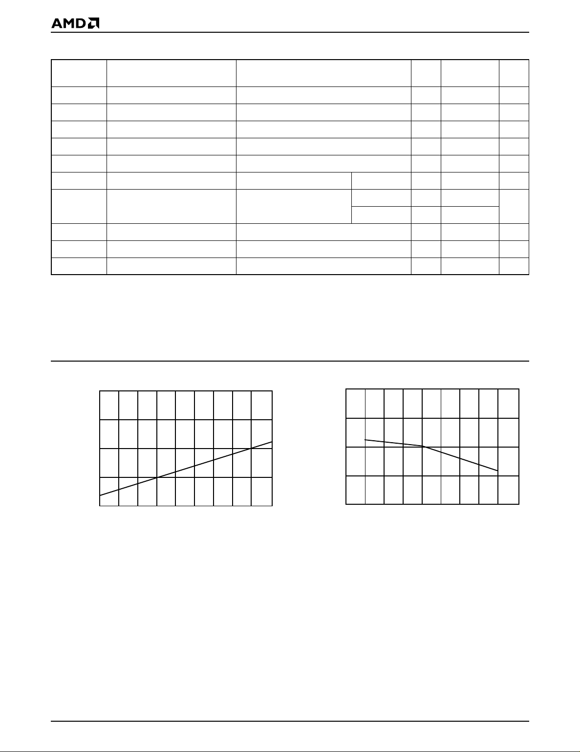
DC CHARACTERISTICS over operating range (unless otherwise specified)
Parameter
Symbol Parameter Description Test Conditions Min Max Unit
V
V
V
V
I
I
CC1
I
CC2
I
CC3
I
PP1
I
LO
OH
OL
IH
IL
LI
Output HIGH Voltage IOH = –400 µA 2.4 V
Output LOW Voltage IOL = 2.1 mA 0.45 V
Input HIGH Voltage 2.0 VCC + 0.5 V
Input LOW Voltage –0.5 +0.8 V
Input Load Current VIN = 0 V to V
Output Leakage Current V
VCC Active Current (Note 2)
VCC TTL Standby Current CE# = V
= 0 V to V
OUT
CE# = V
I
= 0 mA
OUT
, f = 10 MHz,
IL
IH
CC
CC
C/I Devices 30
E Devices 60
1.0
5.0 µA
1.0 mA
VCC CMOS Standby Current CE# = VCC ± 0.3 V 100 µA
VPP Supply Current (Read) CE# = OE# = VIL, VPP = V
CC
100 µA
Caution: The device must not be removed from (or inserted into) a socket when VCC or VPP is applied.
Notes:
1. V
must be applied simultaneously or before VPP, and removed simultaneously or after VPP..
CC
2. I
is tested with OE# = V
CC1
to simulate open outputs.
IH
3. Minimum DC Input Voltage is –0.5 V. During transitions, the inputs may overshoot to –2.0 V for periods less than 20 ns.
Maximum DC Voltage on output pins is V
+ 0.5 V, which may overshoot to VCC + 2.0 V for periods less than 20 ns.
CC
mA
30
25
20
in mA
Supply Current
15
10
12345678910
Frequency in MHz
10205J-5
Figure 1. Typical S upply Current vs. Frequency
V
= 5.5 V, T = 25°C
CC
30
25
20
in mA
15
Supply Current
10
–75 –50 –55 0 25 50 75 100 125 150
Temperature in °C
10205J-6
Figure 2. Typical Sup ply C urr en t vs. Temp er at ure
V
= 5.5 V, f = 10 MHz
CC
8Am27C010
Page 9
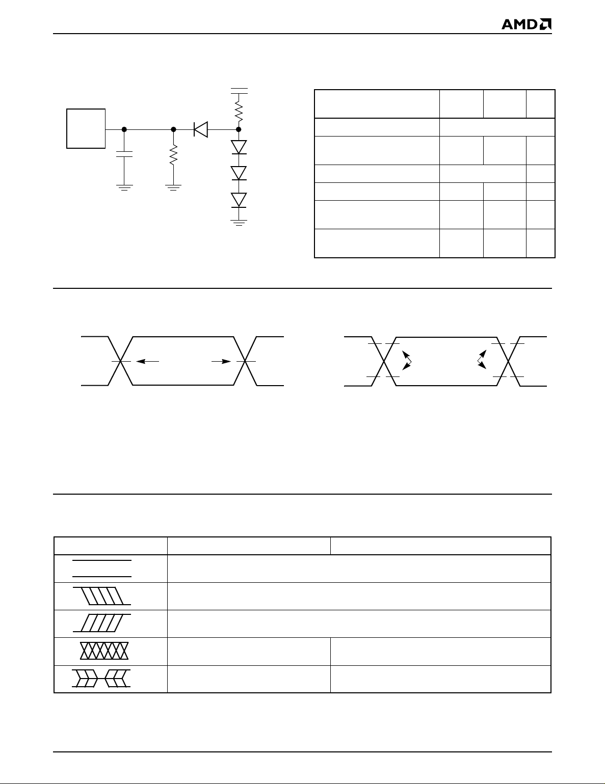
TE S T CONDITIONS
Device
Under
Test
C
L
6.2 kΩ
Note:
Diodes are IN3064 or equivalents.
Figure 3 . Test Setup
SWITCHING TES T WAVEFORM
3 V
1.5 V
0 V
Input Output
Test Points
5.0 V
2.7 kΩ
10205J-7
1.5 V
Table 1. Test Specificati ons
-45,
Test Condition
-55
Output Load 1 TTL gate
Output Load Capacitance, C
(including jig capacitance)
L
30 100 pF
Input Rise and Fall Times ≤ 20 ns
Input Pulse Levels 0.0–3.0 0.45–2.4 V
Input timing measurement
reference levels
Output timing measurement
reference levels
2.4 V
0.45 V
2.0 V
Input Output
1.5 0.8, 2.0 V
1.5 0.8, 2.0 V
Test Points
All
others Unit
2.0 V
0.8 V0.8 V
KEY TO SWITCHING WAVEFORMS
WAVEFORM INPUTS OUTPUTS
Don’t Care, Any Change Permitted Changing, State Unknown
Does Not Apply Center Line is High Impedance State (High Z)
Note: For CL = 100 pF.Note: For CL = 30 pF.
10205J-8
Steady
Changing from H to L
Changing from L to H
KS000010-PAL
Am27C010 9
Page 10
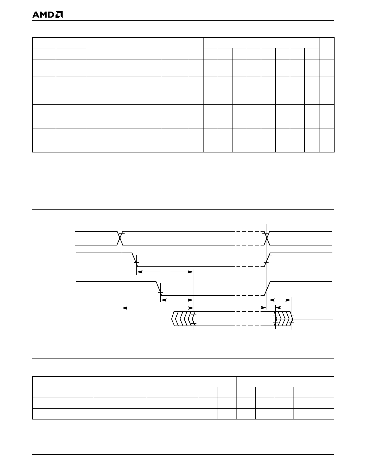
AC CHARACTERISTICS
Parameter Symbols
Am27C010
Description Test Setup
t
AVQV
t
ELQV
t
GLQV
t
EHQZ
t
GHQZ
t
ACC
t
CE
t
OE
t
DF
(Note 2)
Address to Output Delay
Chip Enable to Output Delay OE# = VILMax 45 55 70 90 120 150 200 250 ns
Output Enable to Output
Delay
Chip Enable High or Output
Enable High to Output High Z,
Whichever Occurs First
CE#,
OE# = V
CE# = V
Max 45 55 70 90 120 150 200 250 ns
IL
Max 25 35 35 40 50 65 75 75 ns
IL
Max 25 25 25 25 35 35 40 40 ns
Output Hold Time from
t
AXQX
t
OH
Addresses, CE# or OE#,
Min00000000ns
Whichever Occurs First
Caution: Do not remove the device from (or insert it into) a socket or board that has VPP or V
Notes:
CC
1. VCC must be applied simultaneously or before VPP, and removed simultaneously or after VPP.
2. This parameter is sampled and not 100% tested.
3. Switching characteristics are over operating range, unless otherwise specified.
4. See Figure 3 and Table 1 for test specifications.
SWITCHING WAVEFORMS
2.4
Addresses
0.45
2.0
0.8
Addresses Valid
2.0
0.8
UnitJEDEC Standard -45 -55 -70 -90 -120 -150 -200 -255
applied.
CE#
t
CE
OE#
t
ACC
(Note 1)
Output
High Z
Notes:
1. OE# may be delayed up to t
is specified from OE# or CE#, whichever occurs first.
2. t
DF
– tOE after the falling edge of the addresses without impact on t
ACC
PACKAGE CAPACITANCE
Parameter
Parameter Symbol
C
IN
C
OUT
Notes:
1. This parameter is only sampled and not 100% tested.
2. T
= +25°C, f = 1 MHz.
A
Description Test Conditions
Input Capacitance VIN = 0 9 12 8 12 8 12 pF
Output Capacitance V
= 0 131511141114 pF
OUT
t
OE
Valid Output
t
OH
ACC
High Z
10205J-9
.
CDV032 PL 032 PD 028
UnitTyp Max Typ Max Typ Max
tDF (Note 2)
10 Am27C010
Page 11
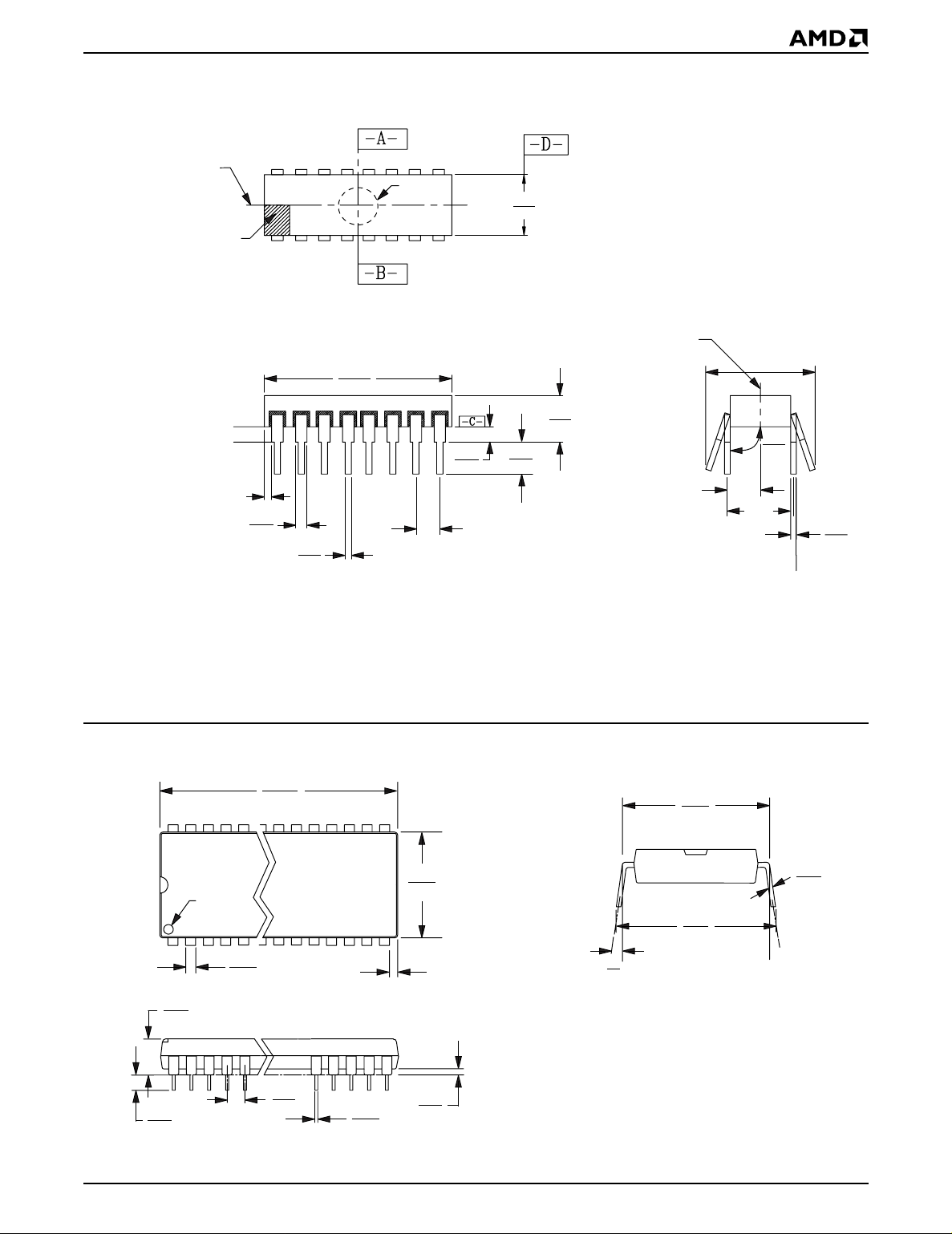
PHYSICAL DIMENSIONS*
CDV032—32-Pin Ceramic Dual In-Line Package, UV Lens (measured in inches)
DATUM D
CENTER PLANE
INDEX AND
TERMINAL NO. 1
I.D. AREA
BASE PLANE
SEATING PLANE
.005 MIN
1
TOP VIEW
1.635
1.680
.045
.065
.014
.026
UV Lens
.100 BSC
.015
.060
.565
.605
.125
.200
CENTER PLANE
.160
.220
DATUM D
.700
MAX
105°
.300 BSC
.600
BSC
94°
.008
.018
SIDE VIEW
* For reference only. BSC is an ANSI standard for Basic Space Centering.
PD 032—32-Pin Plastic Dual In-Line Package (measured in inches)
1.640
1.670
32
.140
.225
Pin 1 I.D.
.045
.065
.005 MIN
17
.530
.580
16
0°
10°
END VIEW
16-000038H-3
CDV032
DF11
3-30-95 ae
.600
.625
.009
.015
.630
.700
.120
.160
.090
.110
.016
.022
SEATING PLANE
.015
.060
16-038-S_AG
PD 032
EC75
5-28-97 lv
Am27C010 11
Page 12
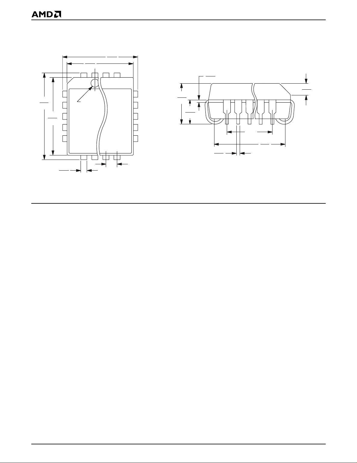
PHYSICAL DIMENSIONS
PL 032—32-Pin Plastic Leaded Chip Carrier (measured in inches)
.485
.495
.009
.015
.125
.140
.080
.095
SEATING
PLANE
.013
.021
.050 REF.
SIDE VIEW
.585
.595
.447
.453
Pin 1 I.D.
.547
.553
.026
.032
TOP VIEW
.042
.056
.400
REF.
.490
.530
16-038FPO-5
PL 032
DA79
6-28-94 ae
l
REVISION SUMMARY
Revision G (May 1998)
Global
Changed formatting to match current data sheets.
Ordering Information—OTP EPROM Products
Valid C ombinations :
options for speed option AM27C010-45, V
Removed the JI and PI package
= 5.0 V ±
CC
10%.
Revision H (January 1999)
Ordering Information—UV EPROM Products
Corrected package type to 32-pin CERDIP.
Revision I (April 26, 1999)
Distinctive Characteristics
Corrected description of packages to 32 pin.
Physical Dimensions
On CerDIP and PDIP package drawings, corrected pin
count to 32.
Revision J (July 2, 1999)
Package Capacitance
Correcte d tabl e he adin g for CDV032.
Trademarks
Copyright © 1999 Advanced Micro Devices, Inc. All rights reserved.
AMD, the AMD logo, and combinations thereof are trademarks of Advanced Micro Devices, Inc.
Flashrite is a trademark of Advanced Micro Devices, Inc.
Product names used in this publication are for identification purposes only and may be trademarks of their respective companies.
12 Am27C010
 Loading...