

Page 1
25AA128/25LC128
25LC128
CS
SO
WP
V
SS
1
2
3
4
8
7
6
5
V
CC
HOLD
SCK
SI
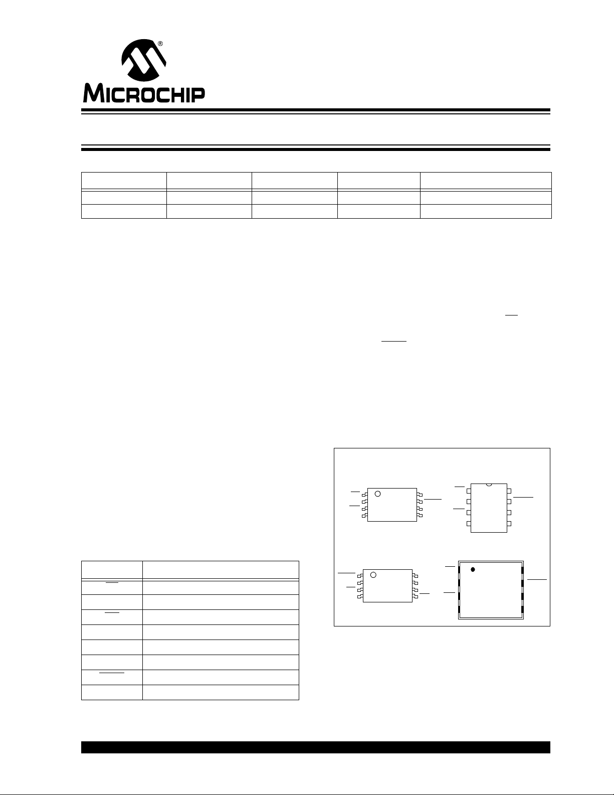
PDIP/SOIC
(P, SN)
TSSOP
CS
SO
WP
V
SS
1
2
3
4
8
7
6
5
V
CC
HOLD
SCK
SI
(ST)
DFN
CS
SO
WP
VSS
HOLD
SCK
SI
25LC128
5
6
7
8
4
3
2
1
VCC
(MF)
X-Rotated TSSOP
HOLD
V
CC
CS
SO
1
2
3
4
8
7
6
5
SCK
SI
V
SS
WP
(X/ST)
128K SPI Bus Serial EEPROM
Device Selection Table
Part Number VCC Range Page Size Temp. Ranges Packages
25LC128 2.5-5.5V 64 Byte I,E P, SN, ST, MF
25AA128 1.8-5.5V 64 Byte I P, SN, ST, MF
Features
• Max. Clock 10 MHz
• Low-power CMOS Technology
- Max. Write Current: 5 mA at 5.5V, 10 MHz
- Read Current: 5 mA at 5.5V, 10 MHz
- Standby Current: 5 μA at 5.5V
• 16,384 x 8-bit Organization
• 64 Byte Page
• Self-tim ed Erase and Write C ycles (5 ms max.)
• Block Write Protection
- Protect none, 1/4, 1/2 or all of array
• Built-in Write Protectio n
- Power-on/off data protection circuitry
- Write enable latch
- Write-protect pin
• Sequential Read
• High Reliability
- Endurance: 1,000,000 erase/write cycles
- Data retention: > 200 years
- ESD protection: > 4000V
• Temperature Ranges Supported;
- Industrial (I): -40°Cto +85°C
- Automotive (E): -40°C to +125°C
• Pb-free and RoHS Compliant
Pin Function Table
Name Function
Description
The Microchip Technology Inc. 25AA128/25LC128
(25XX128
PROMs. The memory is accessed via a simple Serial
Peripheral Interface (SPI) compatible serial bus. The
bus signals required are a clock input (SCK) plus separate data in (SI) and dat a out (SO) lines . Access to the
device is controlled through a Chip Select (CS
Communication to the device can be paused via the
hold pin (HOLD). While the device is paused,
transitions on its inputs will be ignored, with the
exception of Chip Select, allowing the host to service
higher priority interrupts.
The 25XX128 is available in standard packages
including 8-lead PDIP and SOIC, and advanced
packaging including 8-lead DFN and 8-lead TSS OP.
*
) are 128k-bit Serial Electrically Erasable
) input.
Package Types (not to scale)
CS
Chip Select Input
SO Serial Data Output
Write-Protect
Hold Input
WP
SS Ground
V
SI Serial Data Input
SCK Serial Clock Input
HOLD
CC Supply Voltage
V
* 25XX128 is used in this document as a generic part number for the 25AA128, 25LC128 devices.
© 2009 Microchip Technology Inc. DS21831D-page 1
Page 2
25AA128/25LC128
1.0 ELECTRICAL CHARACTERISTICS
Absolute Maximum Ratings
(†)
VCC.............................................................................................................................................................................6.5V
All inputs and outputs w.r.t. V
SS ......................................................................................................... -0.6V to VCC +1.0V
Storage temperature .................................................................................................................................-65°C to 150°C
Ambient temperature under bias...............................................................................................................-40°C to 125°C
ESD protection on all pins..........................................................................................................................................4 kV
† NOTICE: Stresses above those listed under “Absolute Maximum Ratings” may cause permanent damage to the
device. This is a stres s ratin g only and func tional operati on of the devic e at thos e or any other co nditio ns abov e thos e
indicated in the operational listings of this specification is not implied. Exposure to maximum rating conditions for an
extended period of time may affect device reliability.
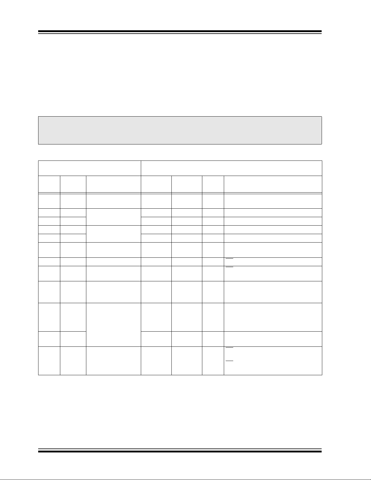
TABLE 1-1: DC CHARACTERISTICS
DC CHARACTERISTICS
Param.
No.
D001 V
Sym. Characteristic Min. Max. Units Test Conditions
IH1 High-level input
voltage
D002 V
D003 VIL2 -0.3 0.2VCC VVCC < 2.7V
D004 V
D005 VOL —0.2VIOL = 1.0 mA, VCC < 2.5V
IL1 Low-level input
voltage
OL Low-level output
voltage
D006 VOH High-level output
voltage
D007 I
LI Input leakage current — ±1 μACS = VCC, VIN = VSS TO VCC
D008 ILO Output leakage
current
D009 CINT Internal Capacit ance
(all inputs and
outputs)
D010 I
CC Read
Operating Current
D011 I
CC Write —
D012 ICCS
Standby Current
Note: This parameter is periodically sampled and not 100% tested.
Industrial (I): TA = -40°C to +85°C VCC = 1.8V to 5.5V
Automotive (E): T
A = -40°C to +125°C VCC = 2.5V to 5.5V
.7 VCC VCC+1 V
-0.3 0.3VCC VVCC ≥ 2.7V
—0.4VIOL = 2.1 mA
VCC -0.5 — V IOH = -400 μA
—±1μACS = VCC, VOUT = VSS TO VCC
—7pFTA = 25°C, CLK = 1.0 MHz,
CC = 5.0V (Note)
V
—
—
5
2.5
mAmAVCC = 5.5V; FCLK = 10.0MHz;
SO = Open
VCC = 2.5V; FCLK = 5.0 MHz;
SO = Open
—
—
—
5
3
5
1
mAmAVCC = 5.5V
V
CC = 2.5V
μAμACS
= VCC = 5.5V, Inputs tied to VCC or
SS, 125°C
V
CS
= VCC = 5.5V, Inputs tied to VCC or
SS, 85°C
V
DS21831D-page 2 © 2009 Microchip Technology Inc.
Page 3
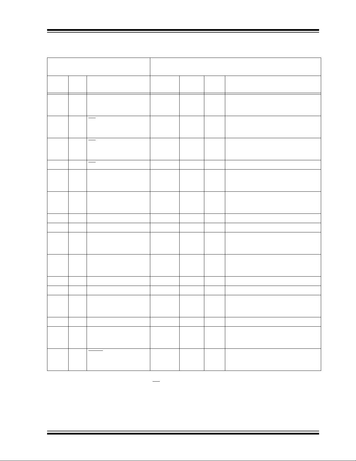
TABLE 1-2: AC CHARACTERISTICS
25AA128/25LC128
AC CHARACTERISTICS
Param.
No.
1F
2T
3T
4T
Sym. Characteristic Min. Max. Units Test Conditions
CLK Clock Frequency —
CSS CS Setup Time 50
CSH CS Hold Time 100
CSD CS Disable Time 50 — ns —
5 Tsu Data Setup Time 10
6THD Data Hold Time 20
7T
8T
9T
10 T
11 T
12 T
13 T
R CLK Rise Time — 100 ns (Note 1)
F CLK Fall Time — 100 ns (Note 1)
HI Clock High Time 50
LO Clock Low Time 50
CLD Clock Delay Time 50 — ns —
CLE Clock Enable Time 50 — ns —
V Output Valid from Clock
Low
14 T
15 T
16 T
HO Output Hold Time 0 — ns (Note 1)
DIS Output Disable Time —
HS HOLD Setup Time 20
Industrial (I): TA = -40°C to +85°C VCC = 1.8V to 5.5V
Automotive (E): T
A = -40°C to +125°C VCC = 2.5V to 5.5V
10
—
—
5
3
—
100
150
—
—
—
200
250
—
—
—
20
30
—
—
—
40
50
—
—
—
100
150
—
—
—
100
150
—
—
—
—
—
50
100
160
40
—
—
80
160
—
40
80
—
—
Note 1: This parameter is periodically sampled and not 100% tested.
2: TWC begins on the risin g e dge of C S af te r a v al id w ri te s eq uen ce and ends when the internal wr i te c ycle is
complete.
3: This parameter is not tested but ensured by characterization. For endurance estimates in a specific
application, plea se con sult th e Tot al End urance ™ Model whic h can be ob t ained from Mi croch ip’ s web s ite:
www.microchip.com.
MHz
MHz
MHz
ns
ns
ns
ns
ns
ns
ns
ns
ns
ns
ns
ns
ns
ns
ns
ns
ns
ns
ns
ns
ns
ns
ns
ns
ns
ns
ns
4.5V ≤ Vcc ≤ 5.5V
2.5V ≤ Vcc < 4.5V
1.8V ≤ Vcc < 2.5V
4.5V ≤ Vcc ≤ 5.5V
2.5V ≤ Vcc < 4.5V
1.8V ≤ Vcc < 2.5V
4.5V ≤ Vcc ≤ 5.5V
2.5V ≤ Vcc < 4.5V
1.8V ≤ Vcc < 2.5V
4.5V ≤ Vcc ≤ 5.5V
2.5V ≤ Vcc < 4.5V
1.8V ≤ Vcc < 2.5V
4.5V ≤ Vcc ≤ 5.5V
2.5V ≤ Vcc < 4.5V
1.8V ≤ Vcc < 2.5V
4.5V ≤ Vcc ≤ 5.5V
2.5V ≤ Vcc < 4.5V
1.8V ≤ Vcc < 2.5V
4.5V ≤ Vcc ≤ 5.5V
2.5V ≤ Vcc < 4.5V
1.8V ≤ Vcc < 2.5V
4.5V ≤ Vcc ≤ 5.5V
2.5V ≤ Vcc < 4.5V
1.8V ≤ Vcc < 2.5V
4.5V ≤ Vcc ≤ 5.5V(Note 1)
2.5V ≤ Vcc ≤ 4.5V(Note 1)
1.8V ≤ Vcc ≤ 2.5V(Note 1)
4.5V ≤ Vcc ≤ 5.5V
2.5V ≤ Vcc < 4.5V
1.8V ≤ Vcc < 2.5V
© 2009 Microchip Technology Inc. DS21831D-page 3
Page 4
25AA128/25LC128
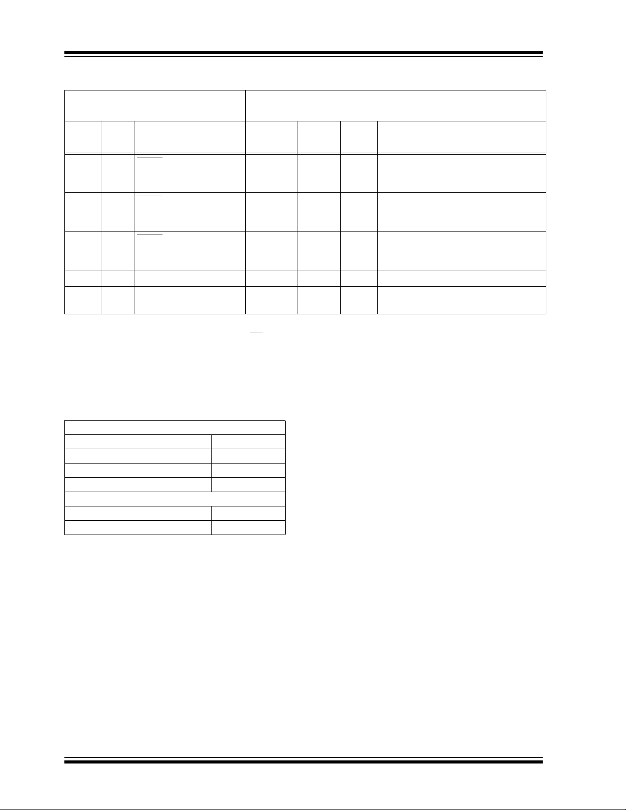
TABLE 1-2: AC CHARACTERISTICS (CONTINUED)
AC CHARACTERISTICS
Param.
No.
Sym. Characteristic Min. Max. Units Test Conditions
Industrial (I): T
Automotive (E): T
17 THH HOLD Hold Time 20
40
80
18 T
HZ HOLD Low to Output
High-Z
30
60
160
19 T
HV HOLD High to Output
Valid
30
60
160
20 T
WC Internal Write Cycle Time — 5 ms (NOTE 2)
A = -40°C to +85°C VCC = 1.8V to 5.5V
A = -40°C to +125°C VCC = 2.5V to 5.5V
—
—
—
—
—
—
—
—
—
ns
ns
ns
ns
ns
ns
ns
ns
ns
21 — Endurance 1,000,000 — E/W
Cycles
Note 1: This parameter is periodically sampled and not 100% tested.
WC begins on the rising e dge of C S af te r a v al id w ri te s eq uence and ends when the interna l w ri te c yc le is
2: T
complete.
3: This parameter is not tested but ensured by characterization. For endurance estimates in a specific
application, plea se con sult th e Tot al End urance ™ Model whic h can be ob t ained from Mi croch ip’ s web s ite:
www.microchip.com.
4.5V ≤ Vcc ≤ 5.5V
2.5V ≤ Vcc < 4.5V
1.8V ≤ Vcc < 2.5V
4.5V ≤ Vcc ≤ 5.5V(Note 1)
2.5V ≤ Vcc < 4.5V(Note 1)
1.8V ≤ Vcc < 2.5V(Note 1)
4.5V ≤ Vcc ≤ 5.5V
2.5V ≤ Vcc < 4.5V
1.8V ≤ Vcc < 2.5V
Page Mode, 25°C, V
CC = 5.5V (NOTE 3)
TABLE 1-3: AC TEST CONDITIONS
AC Waveform:
VLO = 0.2V —
VHI = VCC - 0.2V (Note 1)
HI = 4.0V (Note 2)
V
CL = 50 pF —
Timing Measurement Reference Lev el
Input 0.5 V
Output 0.5 VCC
Note 1: For VCC ≤ 4.0V
2: For V
CC > 4.0V
CC
DS21831D-page 4 © 2009 Microchip Technology Inc.
Page 5
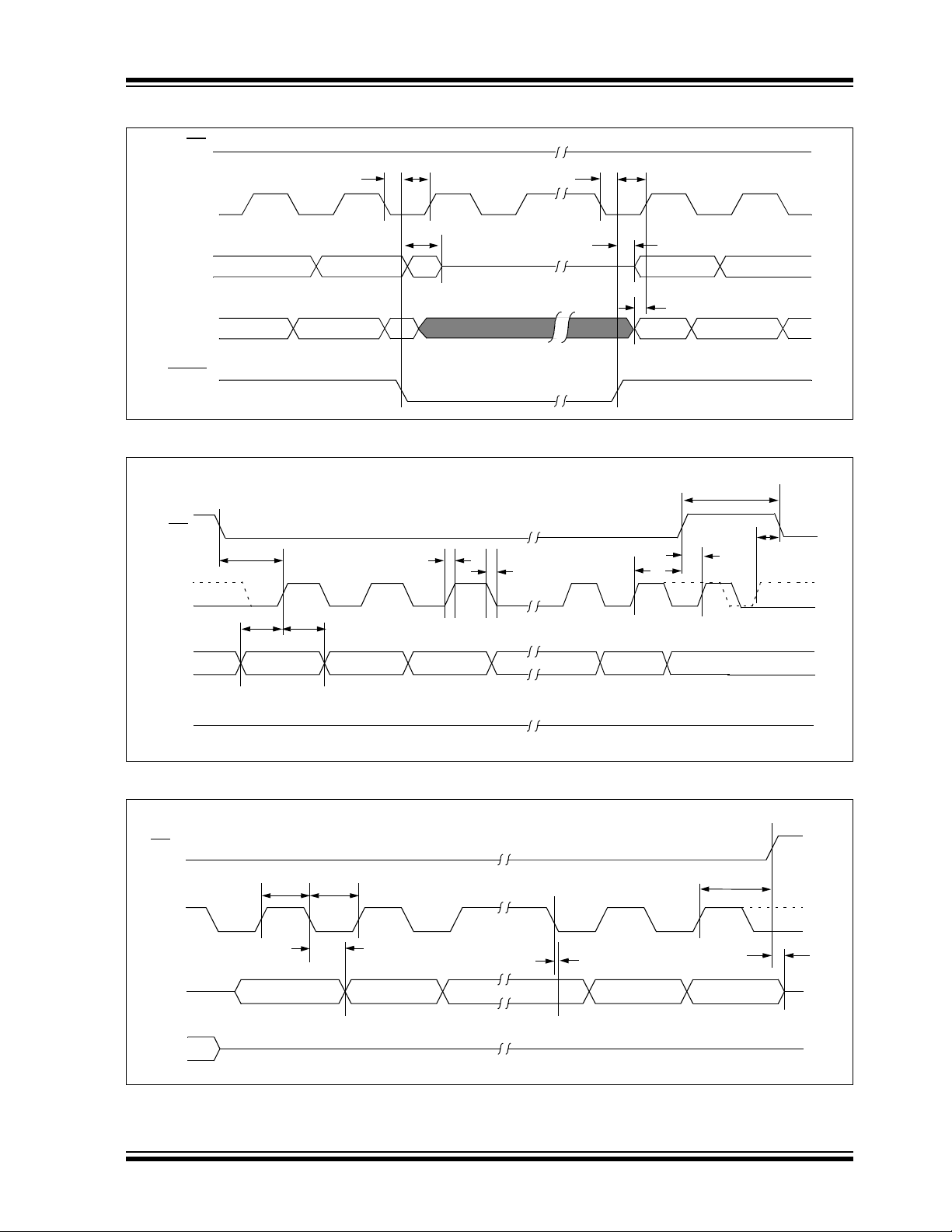
FIGURE 1-1: HOLD TIMING
CS
SCK
SO
SI
HOLD
17
16
16
17
19
18
Don’t Care
5
High-Impedance
n + 2 n + 1 n n - 1
n
n + 2 n + 1 n
n
n - 1
CS
SCK
SI
SO
65
8
7
11
3
LSB in
MSB in
High-Impedance
12
Mode 1,1
Mode 0,0
2
4
CS
SCK
SO
10
9
13
MSB out
ISB out
3
15
Don’t Care
SI
Mode 1,1
Mode 0,0
14
FIGURE 1-2: SERIAL INPUT TIMING
25AA128/25LC128
FIGURE 1-3: SERIAL OUTPUT TIMING
© 2009 Microchip Technology Inc. DS21831D-page 5
Page 6

25AA128/25LC128
2.0 FUNCTIONAL DESCRIPTION
2.1 Principles of Operation
The 25XX128 is a 16,384 byte Serial EEPROM
designed to interf ace di rec tly with the Serial Peripheral
Interface (SPI) port of many of today’s popular
microcontroller families, including Microchip’s PIC
microcontrollers. It may also interface with microcontrollers that do not have a built-i n SPI port by usin g discrete I/O lines programmed properly in firmware to
match the SPI protocol.
The 25XX128 conta ins an 8-bit instr uction regi ster . The
device is accessed via the SI pin, with data being
clocked in on the rising edge of SCK. The CS
be low and the HOLD
operation.
Table 2-1 contains a list of the possible instruction
bytes and format for device operation. All instructions,
addresses and data are transf erred MSB first, LSB last.
Data (SI) is sampled on the first rising edge of SCK
after CS
peripheral devices on the SPI bus, the user can assert
the HOLD
mode. After releasing the HOLD
resume from the point when the HOLD
goes low. If the clock line is sha red wit h ot her
input and place the 25XX128 in ‘HOLD’
pin must be high fo r the entire
pin, operation will
pin must
was asserted.
2.2 Read Sequence
The device is selected by pulling CS low. The 8-bit
READ instruction is transmitted to the 25XX128 followed by the 16-bit address, with two MSBs of the
address being “don’t care” bits. After the correct READ
instruction and add res s a re s en t, the data stored in the
memory at the selected address is shifted out on the
SO pin. The data stored in the memory at the next
address can be read sequentially by continuing to provide clock pulses . The inter nal Address Pointer is automatically incremented to the next higher address after
each byte of data is shifted out. When the highest
address is reached (3FFFh), the address counter rolls
over to address 0000h, allowing the read cycle to be
continued indefi nitely. The read opera tion is te rminated
by raising the CS
pin (Figure 2-1).
2.3 Write Sequence
Prior to any attempt to write data to the 25XX128, the
write enable latch must be set by issuing the WREN
®
instruction (Figure2-4). This is done by setting CS low
and then clocking out the proper instruction into the
25XX128. After all eight bits of the instruction are
transmitted, the CS
write enable latch. If the write operation is initiated
immediately after the WREN instruction without CS
being brought high, the data will not be written to the
array because the write enable latc h will not hav e been
properly set.
Once the write enable latch is set, the user may
proceed by setting the CS
instruction, followed by the 16-bit address, with two
MSBs of the address being “don’t care” bits, and then
the data to be written. Up to 64 bytes of data can be
sent to the device before a write cycle is necessary.
The only restriction is that all of the bytes must reside
in the same page.
Note: Page write operations are limited t o writing
bytes within a single physical page,
regardless of the number of bytes
actually being written. Physical page
boundaries start at addresses that are
integer multiples of the page buffer size (or
‘page size’) and, end at addresses that are
integer multiples of page size – 1. If a
Page Write command attempts to write
across a physical page boundary, the
result is that the data wraps around to the
beginning of the current page (overwriting
data previously stored there), instead of
being written to the next p age as might be
expected. It is therefore necessary for the
application software to prevent page write
operations that would attempt to cross a
page boundary.
For the data to be actually written to the array, the CS
must be brought high a fter the Leas t Significan t bit (D0)
of the n
brought high at any other time, the write operation will
not be completed. Refer to Figure 2-2 and Figure 2-3
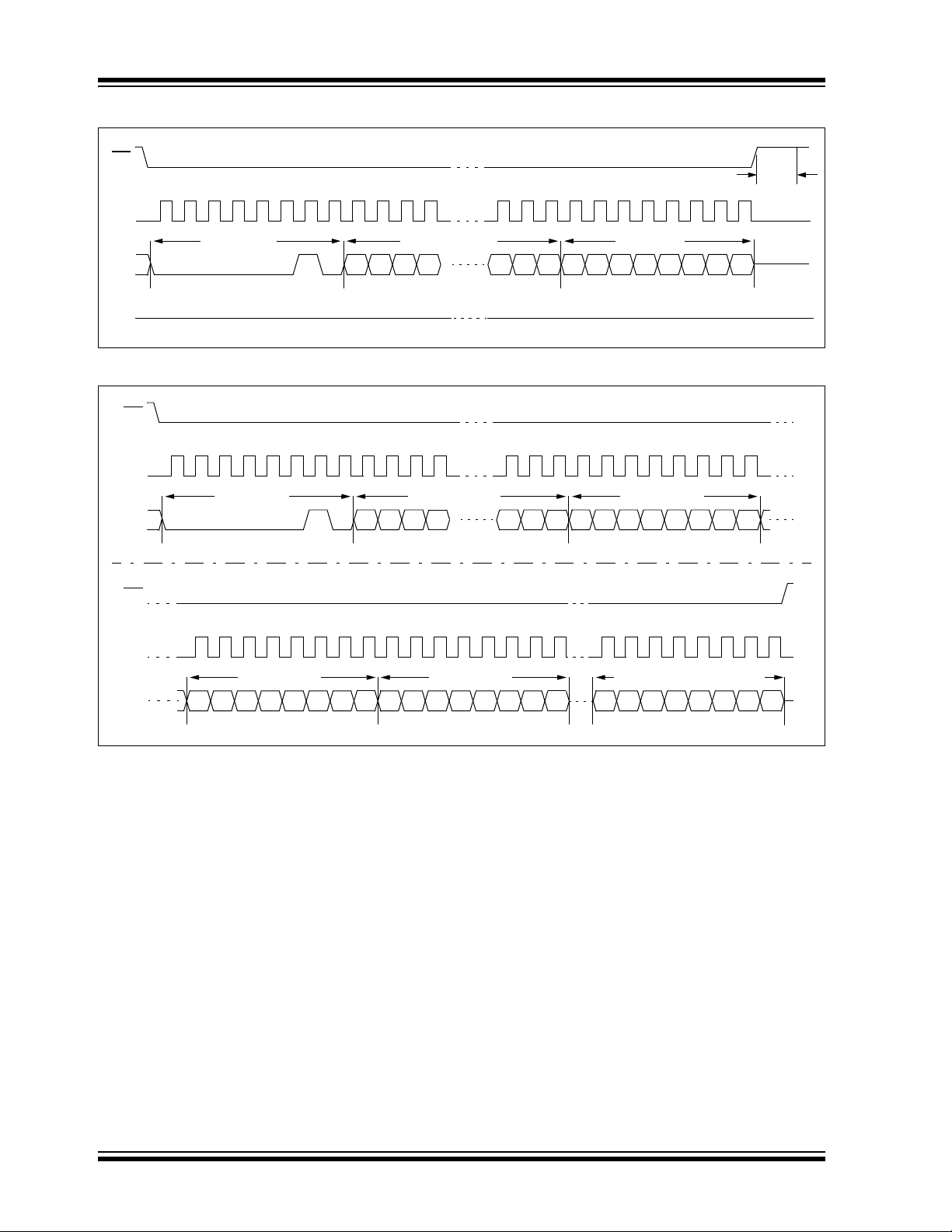
for more detailed illustrations on the byte write
sequence and the page write sequence respectively.
While the write is in progre ss, the ST A TUS regi ster may
be read to check the status of the WPEN, WIP, WEL,
BP1 and BP0 bits (Figure 2-6). A read attempt of a
memory array location will not be possible during a
write cycle. When the write cycle is completed, the
write enable latch is reset.
th
data byte has been clocked in. If CS is
must be brought high to set the
low, issuing a WRITE
DS21831D-page 6 © 2009 Microchip Technology Inc.
Page 7
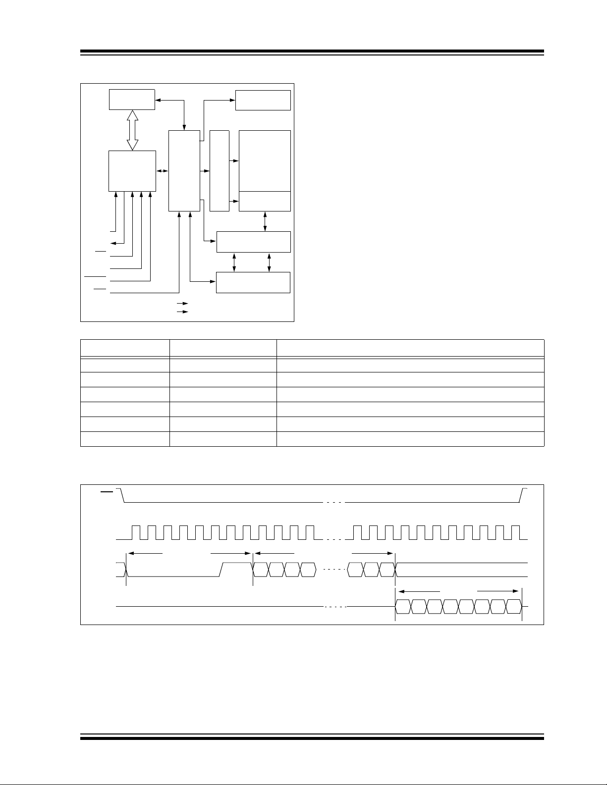
BLOCK DIAGRAM
SI
SO
SCK
CS
HOLD
WP
STATUS
Register
I/O Control
Memory
Control
Logic
X
Dec
HV Generator
EEPROM
Array
Page Latches
Y Decoder
Sense Amp.
R/W Control
Logic
VCC
VSS
SO
SI
SCK
CS
0 234567891011 21222324252627282930311
0100000115 14 13 12 210
76543210
Instruction 16-bit Address
Data Out
High-Impedance
25AA128/25LC128
TABLE 2-1: INSTRUCTION SET
Instruction Name Instruction Format Description
READ
WRITE
WRDI
WREN
RDSR
WRSR
0000 0011
0000 0010
0000 0100
0000 0110
0000 0101
0000 0001
Read data from memory array beginning at selected address
Write data to memory array beginning at selected address
Reset the write enable latch (disable write operations)
Set the write enable latch (enable write operations)
Read STATUS register
Write STATUS register
FIGURE 2-1: READ SEQUENCE
© 2009 Microchip Technology Inc. DS21831D-page 7
Page 8
25AA128/25LC128
SO
SI
CS
91011 2122232425262728293031
0000000115 14 13 12
21076543210
Instruction 16-bit Address Data Byte
High-Impedance
SCK
0 23456718
Twc
SI
CS
9 1011 2122232425262728293031
0000000115 14 13 12
21076543210
Instruction 16-bit Address Data Byte 1
SCK
0 2345671
8
SI
CS
41 42 43 46 47
76543210
Data Byte n (64 max)
SCK
32 34 35 36 37 38 3933
40
76543210
Data Byte 3
76543210
Data Byte 2
44 45
FIGURE 2-2: BYTE WRITE SEQUENCE
FIGURE 2-3: PAGE WRITE SEQUENCE
DS21831D-page 8 © 2009 Microchip Technology Inc.
Page 9
25AA128/25LC128
SCK
0 2345671
SI
High-Impedance
SO
CS
010000 01
SCK
0 2345671
SI
High-Impedance
SO
CS
010000 0
0
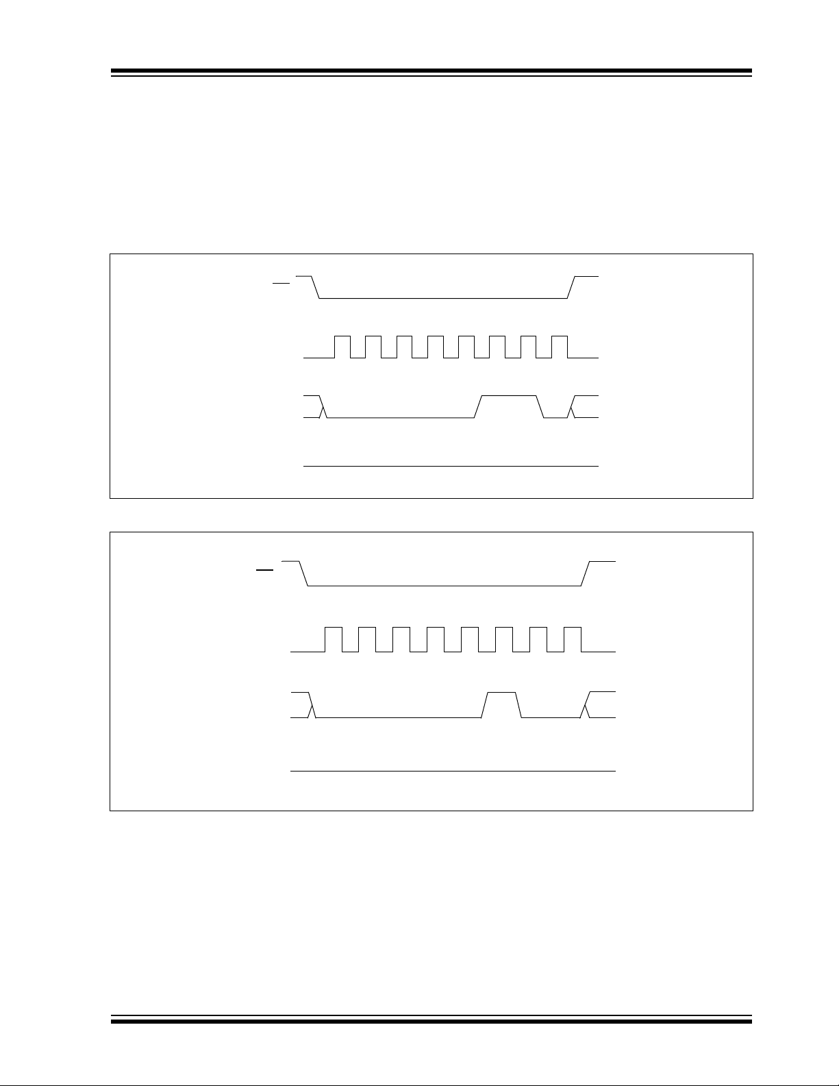
2.4 Write Enable (WREN) and Write
Disable (WRDI)
The 25XX128 contains a write enable latch. See
T abl e 2-4 for the Write-Protect func tionality ma trix. This
latch must be set before any write operation will be
completed internally. The WREN instruction will set the
latch, and the WRDI will reset the latch.
FIGURE 2-4: WRITE ENABLE SEQUENCE (WREN)
The following is a list of conditions under which the
write enable latch will be reset:
• Power-up
• WRDI instruction successfully executed
• WRSR instruction successfully executed
• WRITE instruction successfully executed
FIGURE 2-5: WRITE DISABLE SEQUENCE (WRDI)
© 2009 Microchip Technology Inc. DS21831D-page 9
Page 10
25AA128/25LC128
SO
SI
CS
9101112131415
11000000
7654 210
Instruction
Data from STATUS Register
High-Impedance
SCK
0 2345671
8
3
2.5 Read Status Regist er Instruction
(RDSR)
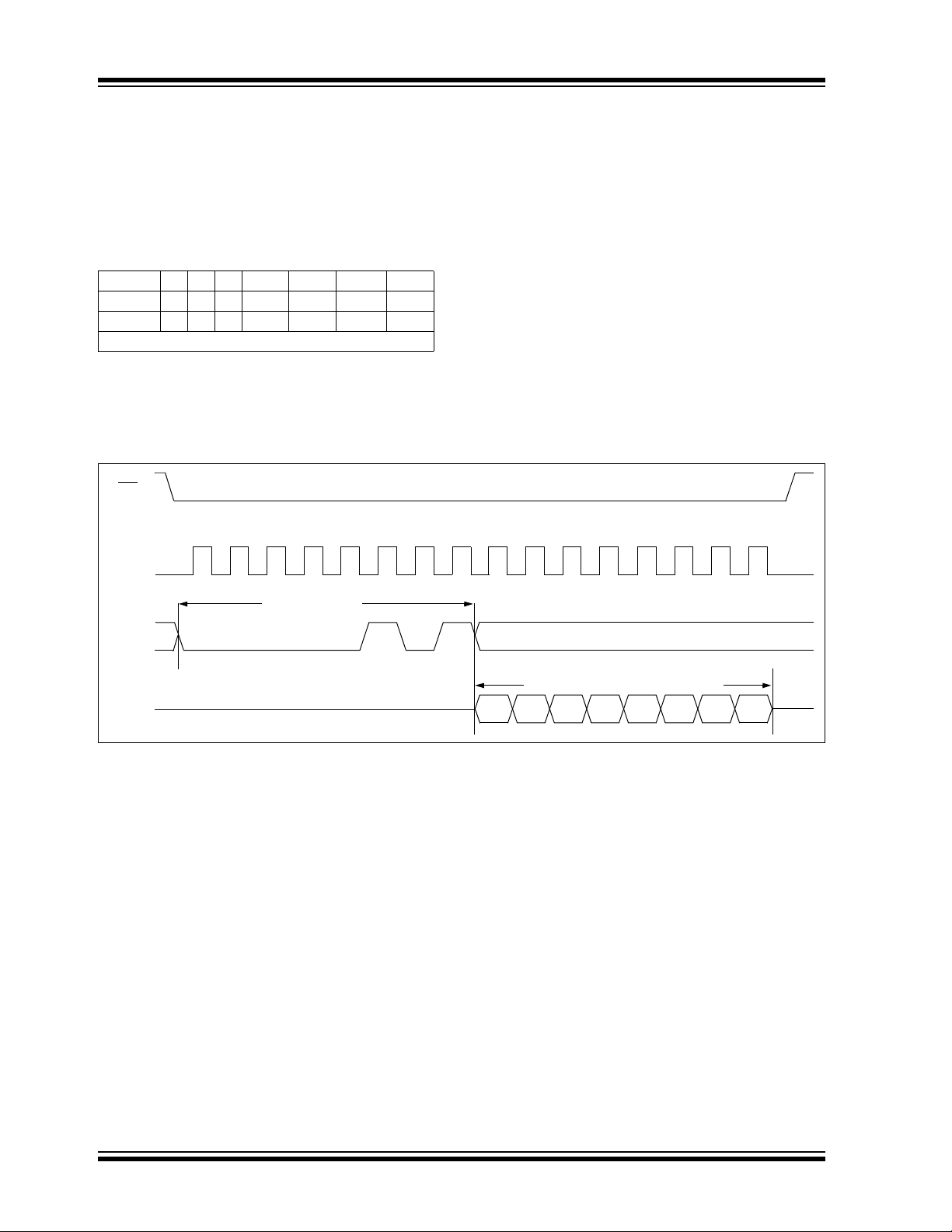
The Read Status Register instruction (RDSR) provides
access to the STATUS register. The STATUS register
may be read at any time, ev en during a wri te cycle. The
STATUS register is formatted as follows:
TABLE 2-2: STATUS REGISTER
7 654 3 2 1 0
W/R –––W/RW/R R R
WPEN X X X BP1 BP0 WEL WIP
W/R = writable/readable. R = read-only.
The Write-In-Process (WIP) bit indicates whether the
25XX128 is busy with a write operation. When set to a
1’, a write is in progress, when set to a ‘0’, no write is
‘
in progress. This bit is read-only.
The Wri te Enable Lat ch (WEL) bit indicat es the st atus
of the write enabl e la tch and i s read -o nly. When set to
a ‘
1’, the latch allows writes to the array, when set to a
0’, the latch prohibits writes to the array. The state of
‘
this bit can always be updated via the WREN or WRDI
commands regardless of the state of write protection
on the STATUS register. These commands are shown
in Figure 2-4 and Figure 2-5.
The Block Protection (BP0 and BP1) bits indicate
which blocks are currently write-protected. These bits
are set by the user issuing the WRSR instruction . These
bits are nonvolatile, and are shown in Table 2-3.
See Figure 2-6 for the RDSR timing sequence.
FIGURE 2-6: READ STATUS REGISTER TIMING SEQUENCE (RDSR)
DS21831D-page 10 © 2009 Microchip Technology Inc.
Page 11
2.6 Write Status Register (WRSR)
SO
SI
CS
9101112131415
01000000
7654
210
Instruction Data to STATUS Register
High-Impedance
SCK
0 23456718
3
25AA128/25LC128
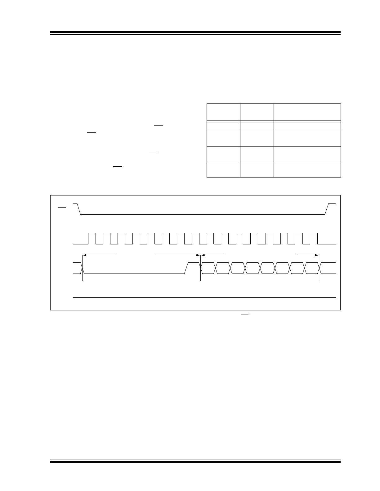
The Write Status Register (WRSR) instruction allows the
user to write to the nonvolatile bits in the STATUS register as shown in Table 2-2. The user is able to select
one of four levels of protection for the array by writing
to the appropriate bits in the STATUS register. The
array is divided up into four segments . The user has the
ability to write-protect none, one, two, or all four of the
segments of the array. The partitioning is controlled as
shown in Table 2-3.
The Write-Protect Enable (WPEN) bit is a nonvolatile
bit that is available as an enable bi t for the WP
Write-Protect (WP
(WPEN) bit in the STATUS register control the
programmable hardware write-protect feature. Hardware write protection is enabled when WP
and the WPEN bit is high. Hardware write protection is
disabled when either the WP
bit is low. When the chip is hardware write-protected,
) pin and the Write-Protect Enable
pin is high or the WPEN
pin. The
pin is low
only writes to nonvolatile bits in the STATUS register
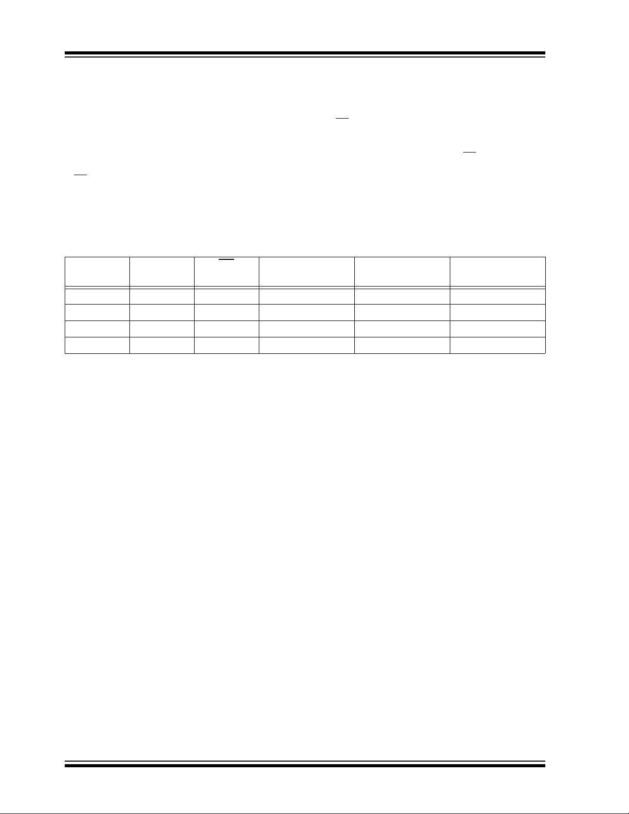
are disabled. See Table 2-4 for a matrix of functionality
on the WPEN bit.
See Figure 2-7 for the WRSR timing sequence.
TABLE 2-3: ARRAY PROTECTION
BP1 BP0
00
01
10
11
FIGURE 2-7: WRITE STATUS REGISTER TIMING SEQUENCE (WRSR)
Array Addresses
Write-Protected
none
upper 1/4
(3000h-3FFFh)
upper 1/2
(2000h-3FFFh)
all
(0000h-3FFFh)
Note: An internal write cycle (TWC) is initiated on the rising edge of CS after a valid write STATUS register
© 2009 Microchip Technology Inc. DS21831D-page 11
Page 12
25AA128/25LC128
2.7 Data Protection
The following protection has been implemented to
prevent in advertent writes to the array:
• The write enable latch is reset on power-up
• A write enable instruction must be issued to set
the write enable latch
• After a byte write, page write or STATUS register
write, the write enable latch is reset
must be set high after the proper number of
•CS
clock cycles to start an internal write cycle
• Access to the array during an internal write cycle
is ignored and programming is continued
2.8 Power-On State
The 25XX128 powers on in the following state:
• The device is in low-power Standby mode
(CS
• The write enable latch is reset
• SO is in high-impedance state
• A high-to-low-level transition on CS
enter active state
TABLE 2-4: WRITE-PROTECT FUNCTIONALITY MATRIX
WEL
(SR bit 1)
0xx
10x
1
1
WPEN
(SR bit 7)
1
1
WP
(pin 3)
0 (low)
1 (high)
Protected Blocks Unprotected Blocks STATUS Register
Protected Protected Protected
Protected Writable Writable
Protected Writable Protected
Protected Writable Writable
x = don’t care
= 1)
is required to
DS21831D-page 12 © 2009 Microchip Technology Inc.
Page 13
25AA128/25LC128
3.0 PIN DESCRIPTIONS
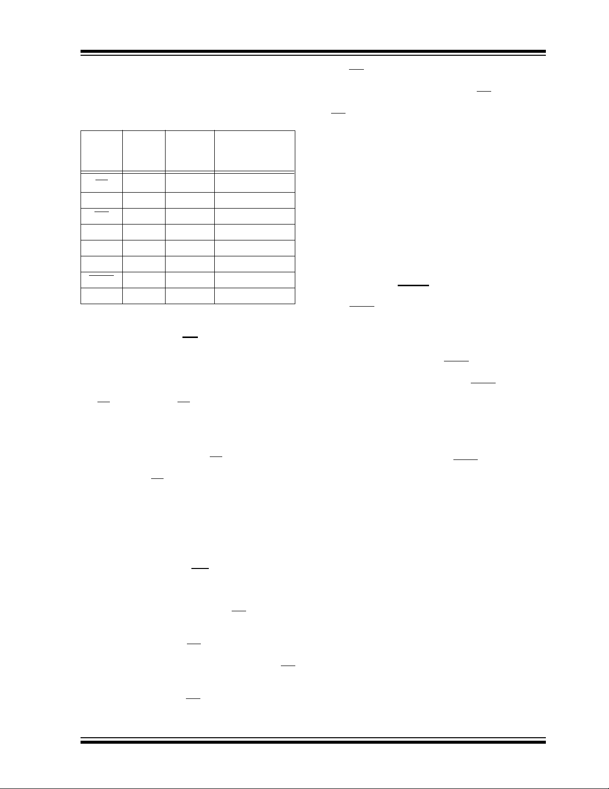
The descriptions of the pins are listed in Table 3-1.
TABLE 3-1: PIN FUNCTION TABLE
Name
CS
SO 2 4 Serial Data Output
WP 3 5 Write-Protect Pin
V
SS 4 6 Ground
SI 5 7 Serial Data Input
SCK 6 8 Serial Clock Input
HOLD
V
CC 8 2 Supply Voltage
Note: The exposed pad on the DFN package
Pin
Number
can be connected to VSS or left floating.
3.1 Chip Select (CS)
A low level on this pin selects the device. A high level
deselects the device and forces it into Standby mode.
However, a programming cycle which is already
initiated or in progress will be completed, regardle ss of
the CS input signal. If CS is brought high during a
program cycle, the de vice wil l go into S t andb y mode as
soon as the programming cycle is complete. When the
device is deselected, SO goes to the high-impedance
state, allowing multiple parts to share the same SPI
bus. A low-to-high transition on CS
sequence initiates an internal write cycle. After powerup, a low level on CS is r equ ired p r ior to any sequence
being initiated.
X-Rotated
Pin
Number
1 3 Chip Select Input
7 1 Hold Input
Function
after a valid write
The WP
the STATUS register is low. This allows the user to
install the 25XX128 in a system with WP pin grounded
and still be able to write to the STATUS register. The
WP
set high.
pin function is blocked when the WPEN bit in
pin functions will be enabled when the WPEN bit is
3.4 Serial In p u t (SI)
The SI pin is used to transfer data into the device. It
receives instructions, addresses and data. Data is
latched on the rising edge of the serial clock.
3.5 Serial Clock (SCK)
The SCK is used to synchronize the communication
between a master and the 25XX128. Instructions,
addresses or data pres en t on th e SI pin are latched on
the rising edge of t he c lo ck in put, while data on the SO
pin is updated after the falling edge of the clock input.
3.6 Hold (HOLD)
The HOLD pin is used to suspend transmission to the
25XX128 while in the mid dle of a seri al sequ ence wit hout having to retransmit the entire sequence again. It
must be held high any time this function is not being
used. Once the device is selected and a serial
sequence is underway, the HOLD
low to pause further serial communication without
resetting the serial sequence. The HOLD pin must be
brought low while SCK is low, otherwise the HOLD
function will not be invoked until the next SCK high-tolow transition. The 25XX128 must remain selected
during this sequence. The SI, SCK and SO pins are in
a high-impedance state during the time the device is
paused and transitions on these p ins will be ignored. To
resume serial communication, HOLD
high while the SCK pin is low, otherwise serial
communication will not resume. Lowering the HOLD
line at any time will tri-state the SO line.
pin may be pulled
must be brought
3.2 Serial Output (SO)
The SO pin is used to transfer data out of the 25XX128.
During a read cycle, data is shifted out on this pin after
the falling edge of the serial clock.
3.3 Write-Protect (WP)
This pin is used in conjunction with the WPEN bit in the
STATUS register to prohibit writes to the nonvolatile
bits in the STATUS register. When WP is low and
WPEN is high, writing to the nonvolatile bits in the
STATUS register is disabled. All other operations
function normally. When WP
including writes to the nonvolatile bits in the STATUS
register, operate normally. If the WPEN bit is set, WP
low during a STATUS register write sequence will disable writing to the STATUS register. If an internal write
cycle has already begun, WP
effect on the write.
© 2009 Microchip Technology Inc. DS21831D-page 13
is high, all functions,
going low will have no
Page 14
25AA128/25LC128
T/XXXNNN
XXXXXXXX
YYWW
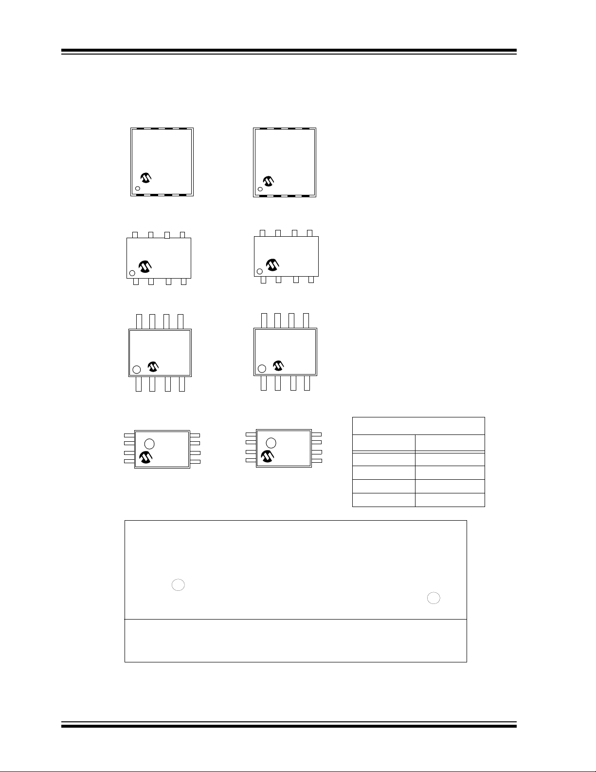
8-Lead PDIP
8-Lead SOIC
T/XXYYWW
XXXXXXXX
NNN
XXXX
TYWW
8-Lead TSSOP
NNN
I/P 1L7
25AA128
0328
Example:
Example:
I/SN 0328
25LC128
1L7
1L7
5LD
I328
Example:
8-Lead DFN
Example
:
XXXXXXX
T/XXXXX
YYWW
25LC128
I/MF
0328
1L7
NNN
Legend: XX...X Customer-specific information
Y Year code (last digit of calendar year)
YY Year code (last 2 digits of calendar year)
WW Week code (week of January 1 is week ‘01’)
NNN Alphanumeric traceability code
Pb-free JEDEC designator for Matte Tin (Sn)
* This package is Pb-free. The Pb-free JEDEC designator ( )
can be found on the outer packaging for this package.
Note: In the event the full Microchip part nu mber ca nnot be m arked on one line , it will
be carried over to the next line, thus limiting the number of available
characters for customer-specific information.
3
e
3
e
TSSOP 1st Line Marking
Device std mark
25AA128 5AD
25AA128X 5ADX
25LC128 5LD
25LC128X 5LDX
4.0 PACKAGING INFORMATION
4.1 Package Marking Information
DS21831D-page 14 © 2009 Microchip Technology Inc.
Page 15
25AA128/25LC128
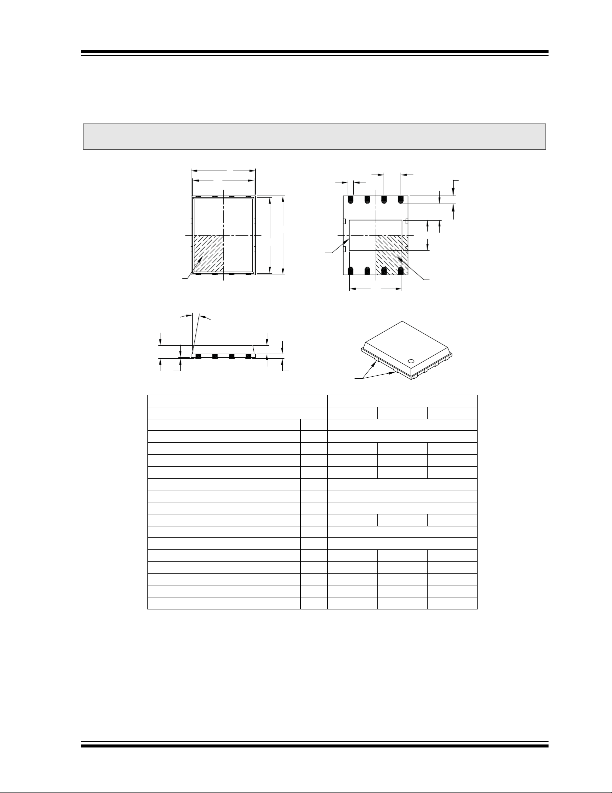
8-Lead Plastic Dual Flat, No Lead Package (MF) – 6x5 mm Body [DFN-S]
PUNCH SINGULATED
Notes:
1. Pin 1 visual index feature may vary, but must be located within the hatched area.
2. Package may have one or more exposed tie bars at ends.
3. Dimensioning and tolerancing per ASME Y14.5M.
BSC: Basic Dimension. Theoretically exact value shown without tolerances.
REF: Reference Dimension, usually without tolerance, for information purposes only.
Note: For the most current package drawings, please see the Microchip Packaging Specification located at
http://www.microchip.com/packaging
Units MILLIMETERS
Dimension Limits MIN NOM MAX
Number of Pins N 8
Pitch e 1.27 BSC
Overall Height A – 0.85 1.00
Molded Package Thickness A2 – 0.65 0.80
Standoff A1 0.00 0.01 0.05
Base Thickness A3 0.20 REF
Overall Length D 4.92 BSC
Molded Package Length D1 4.67 BSC
Exposed Pad Length D2 3.85 4.00 4.15
Overall Width E 5.99 BSC
Molded Package Width E1 5.74 BSC
Exposed Pad Width E2 2.16 2.31 2.46
Contact Width b 0.35 0.40 0.47
Contact Length L 0.50 0.60 0.75
Contact-to-Exposed Pad K 0.20 – –
Model Draft Angle Top φ – – 12°
φ
NOTE 2
A3
A2
A1
A
NOTE 1
NOTE 1
EXPOSED
PAD
BOTTOM VIEW
1
2
D2
2
1
E2
K
L
N
e
b
E
E1
D
D1
N
TOP VIEW
Microchip Technology Drawing C04-113B
© 2009 Microchip Technology Inc. DS21831D-page 15
Page 16
25AA128/25LC128
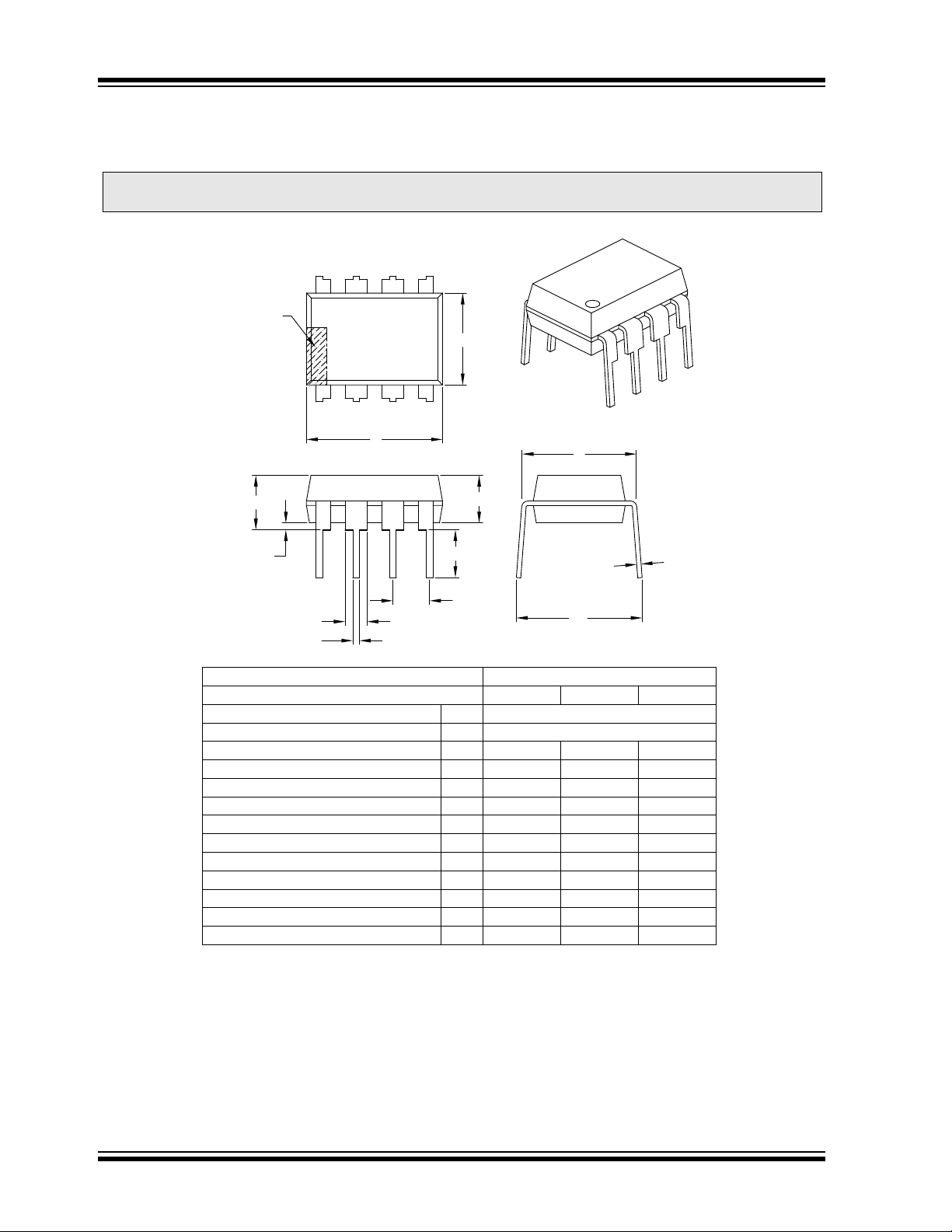
8-Lead Plastic Dual In-Line (P) – 300 mil Body [PDIP]
Notes:
1. Pin 1 visual index feature may vary, but must be located with the hatched area.
2. § Significant Characteristic.
3. Dimensions D and E1 do not include mold flash or protrusions. Mold flash or protrusions shall not exceed .010" per side.
4. Dimensioning and tolerancing per ASME Y14.5M.
BSC: Basic Dimension. Theoretically exact value shown without tolerances.
Note: For the most current package drawings, please see the Microchip Packaging Specification located at
http://www.microchip.com/packaging
Units INCHES
Dimension Limits MIN NOM MAX
Number of Pins N 8
Pitch e .100 BSC
Top to Seating Plane A – – .210
Molded Package Thickness A2 .115 .130 .195
Base to Seating Plane A1 .015 – –
Shoulder to Shoulder Width E .290 .310 .325
Molded Package Width E1 .240 .250 .280
Overall Length D .348 .365 .400
Tip to Seating Plane L .115 .130 .150
Lead Thickness c .008 .010 .015
Upper Lead Width b1 .040 .060 .070
Lower Lead Width b .014 .018 .022
Overall Row Spacing § eB – – .430
N
E1
NOTE 1
D
12
3
A
A1
A2
L
b1
b
e
E
eB
c
Microchip Technology Drawing C04-018B
DS21831D-page 16 © 2009 Microchip Technology Inc.
Page 17
25AA128/25LC128
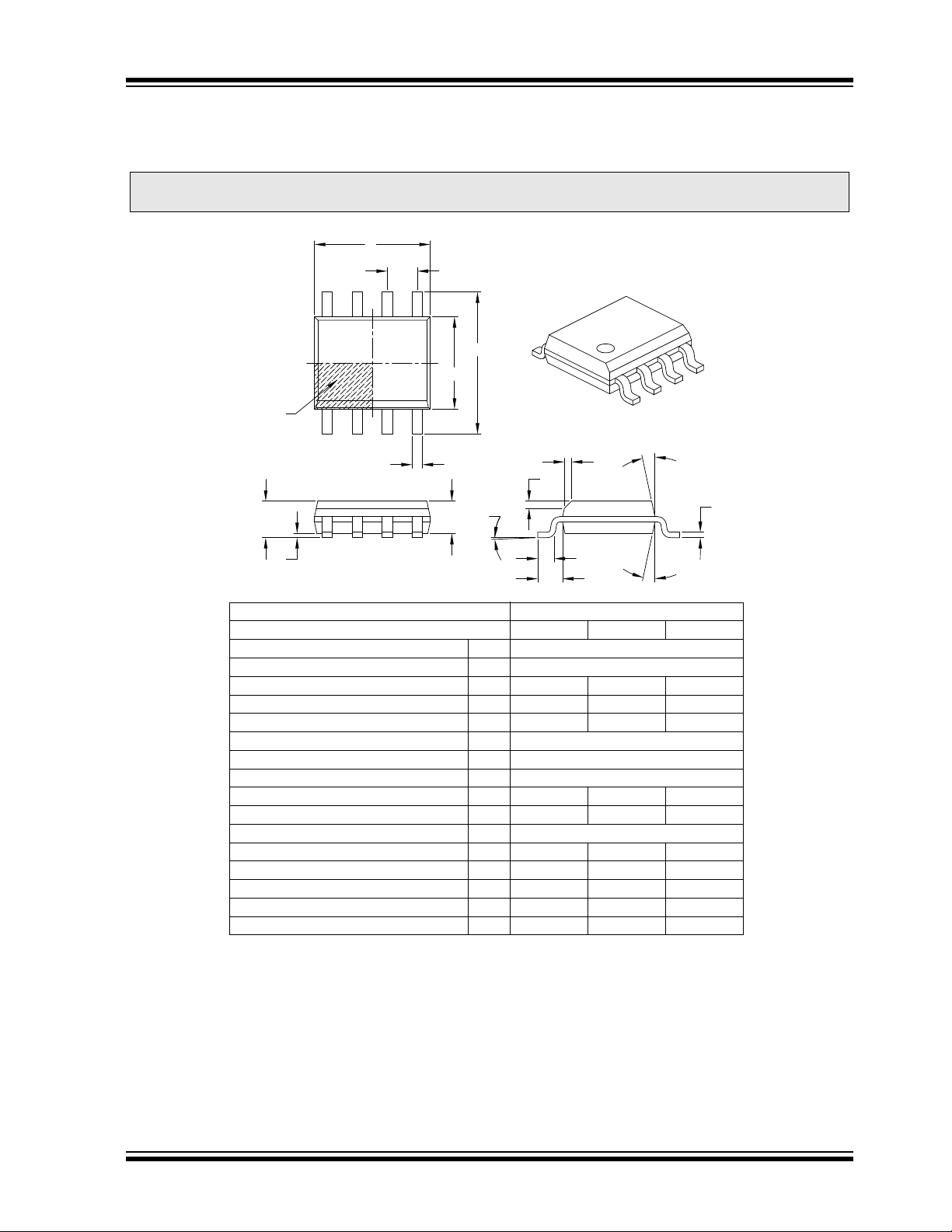
8-Lead Plastic Small Outline (SN) – Narrow, 3.90 mm Body [SOIC]
Notes:
1. Pin 1 visual index feature may vary, but must be located within the hatched area.
2. § Significant Characteristic.
3. Dimensions D and E1 do not include mold flash or protrusions. Mold flash or protrusions shall not exceed 0.15 mm per side.
4. Dimensioning and tolerancing per ASME Y14.5M.
BSC: Basic Dimension. Theoretically exact value shown without tolerances.
REF: Reference Dimension, usually without tolerance, for information purposes only.
Note: For the most current package drawings, please see the Microchip Packaging Specification located at
http://www.microchip.com/packaging
Units MILLIMETERS
Dimension Limits MIN NOM MAX
Number of Pins N 8
Pitch e 1.27 BSC
Overall Height A – – 1.75
Molded Package Thickness A2 1.25 – –
Standoff
§
A1 0.10 – 0.25
Overall Width E 6.00 BSC
Molded Package Width E1 3.90 BSC
Overall Length D 4.90 BSC
Chamfer (optional) h 0.25 – 0.50
Foot Length L 0.40 – 1.27
Footprint L1 1.04 REF
Foot Angle φ 0° – 8°
Lead Thickness c 0.17 – 0.25
Lead Width b 0.31 – 0.51
Mold Draft Angle Top α 5° – 15°
Mold Draft Angle Bottom β 5° – 15°
D
N
e
E
E1
NOTE 1
12 3
b
A
A1
A2
L
L1
c
h
h
φ
β
α
Microchip Technology Drawing C04-057B
© 2009 Microchip Technology Inc. DS21831D-page 17
Page 18
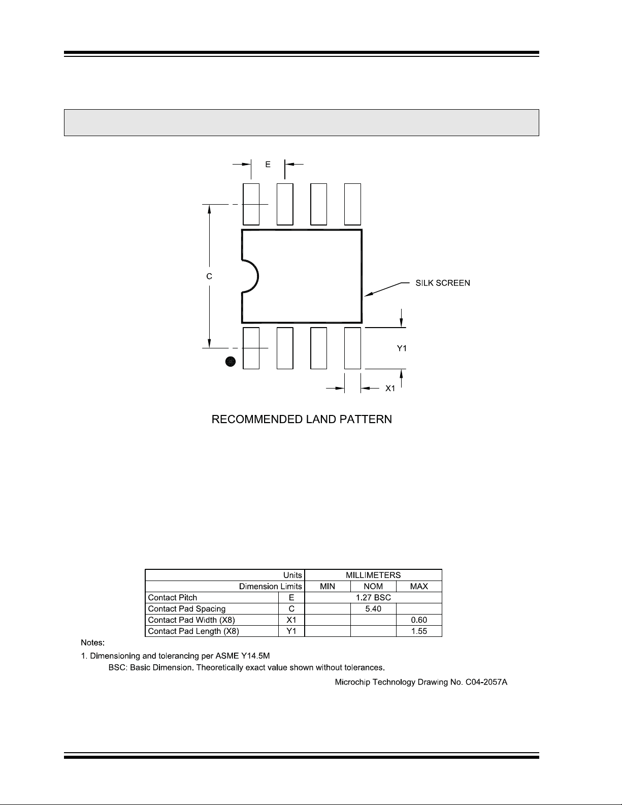
25AA128/25LC128
!"#$%
& !"#$%!&!!'#($
)**%%% *#
DS21831D-page 18 © 2009 Microchip Technology Inc.
Page 19
25AA128/25LC128
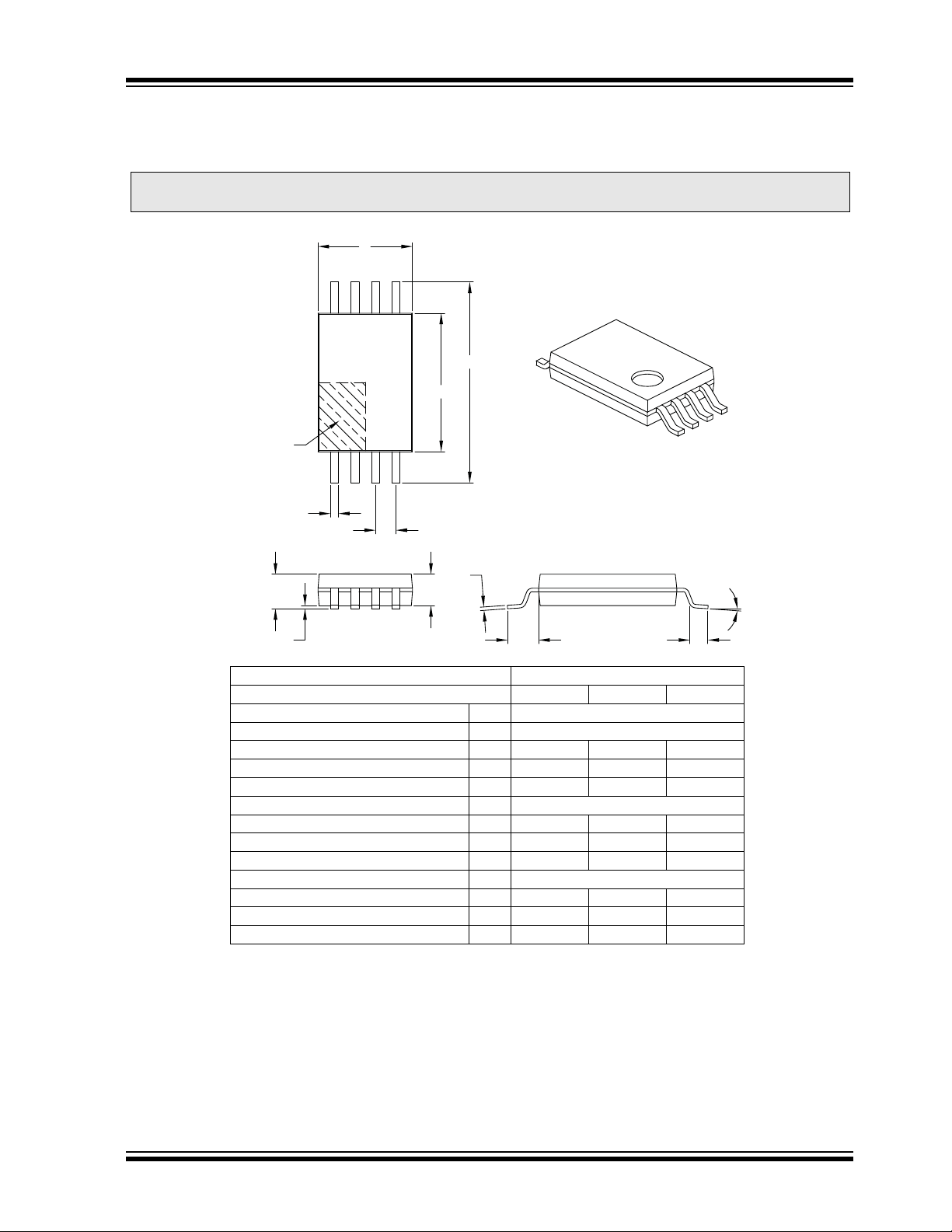
8-Lead Plastic Thin Shrink Small Outline (ST) – 4.4 mm Body [TSSOP]
Notes:
1. Pin 1 visual index feature may vary, but must be located within the hatched area.
2. Dimensions D and E1 do not include mold flash or protrusions. Mold flash or protrusions shall not exceed 0.15 mm per side.
3. Dimensioning and tolerancing per ASME Y14.5M.
BSC: Basic Dimension. Theoretically exact value shown without tolerances.
REF: Reference Dimension, usually without tolerance, for information purposes only.
Note: For the most current package drawings, please see the Microchip Packaging Specification located at
http://www.microchip.com/packaging
Units MILLIMETERS
Dimension Limits MIN NOM MAX
Number of Pins N 8
Pitch e 0.65 BSC
Overall Height A – – 1.20
Molded Package Thickness A2 0.80 1.00 1.05
Standoff A1 0.05 – 0.15
Overall Width E 6.40 BSC
Molded Package Width E1 4.30 4.40 4.50
Molded Package Length D 2.90 3.00 3.10
Foot Length L 0.45 0.60 0.75
Footprint L1 1.00 REF
Foot Angle φ 0° – 8°
Lead Thickness c 0.09 – 0.20
Lead Width b 0.19 – 0.30
D
N
E
E1
NOTE 1
12
b
e
c
A
A1
A2
L1
L
φ
Microchip Technology Drawing C04-086B
© 2009 Microchip Technology Inc. DS21831D-page 19
Page 20

25AA128/25LC128
APPENDIX A: REVISION HISTORY
Revision B
Corrections to Section 1.0, Electrical Characteristics.
Revision C (5/07)
Removed Preliminary status; Revised Table 1-2, Para.
7 and 8; Revised Table 1-3, CL; Revised trademarks;
Replaced Package drawings (Rev. AP); Replaced OnLine Support; Revised Product ID section.
Revision D (06/09)
Added X-Rotated TSSOP to package types; Revised
Table 1-2, Param. 21; Revised Table 3-1; Revised
TSSOP Line Marking tab le; Added SOI C Land Pattern;
Revised Product ID section.
DS21831D-page 20 © 2009 Microchip Technology Inc.
Page 21

25AA128/25LC128
THE MICROCHIP WEB SITE
Microchip provides onlin e support v ia our W WW site at
www.m ic roc hi p.c om . Thi s web si te i s us ed as a m ean s
to make files and information easily available to
customers. Accessible by using your favorite Internet
browser, the web site contains the following
information:
• Product Support – Data sheets and errata,
application notes and sample programs, design
resources, user’s guides and hardware support
documents, latest software releases and archived
software
• General Technical Support – Frequently Asked
Questions (FAQ), technical support requests,
online discussion groups, Microchip consultan t
program member listing
• Business of Microchip – Product selector and
ordering guides, latest Microchip press releases,
listing of s eminars and events, listings of
Microchip sales offices, distributors and factory
representatives
CUSTOMER CHANGE NOTIFICATION SERVICE
CUSTOMER SUPPORT
Users of Microchip products can receive assistance
through several channels:
• Distributor or Representative
• Local Sales Office
• Field Application Engineer (FAE)
• Technical Support
• Development Systems Information Line
Customers should contact their distributor,
representative or field application engineer (FAE) for
support. Local sales offices are also available to help
customers. A listing of sales offices and locations is
included in the back of this document.
T echnic al suppo rt is avail able throug h the web si te
at: http://support.microchip.com
Microchip’s customer notification service helps keep
customers current on Microchip products. Subscribers
will receive e-mail notification whenever there are
changes, updates, revisions or errata related to a
specified produ ct family or develo pment tool of inte rest.
To register, access the Microchip web site at
www.microchip.com, click on Customer Change
Notification and follow the registration instructions.
© 2009 Microchip Technology Inc. DS21831D-page 21
Page 22

25AA128/25LC128
To:
Technical Publications Manager
RE: Reader Response
Total Pages Sent ________
From:
Name
Company
Address
City / State / ZIP / Country
Telephone: (_______) _________ - _________
Application (optional):
Would you like a reply? Y N
Device: Literature Number:
Questions:
FAX: (______) _________ - _________
DS21831D25AA128/25LC128
READER RESPONSE
It is our intentio n to pro vi de you with the best documentation possible to ens ure suc c es sfu l u se of y ou r M ic roc hip product. If you wish to provid e your c omment s on org anizatio n, clarity, subject matter , and ways in w hich o ur document atio n
can better serve you, please FAX your comments to the Technical Publications Manager at (480) 792-4150.
Please list the following information, and use this outline to provide us with your comments about this document.
1. What are the best featur es of this document?
2. How does this document meet your hardware and software development needs?
3. Do you find the organization of this document easy to follow? If not, why?
4. What additions to the document do you think would enhance the structure and subject?
5. What deletions from the document could be made without affecting the overall usefulness?
6. Is there any incorrect or misleading information (what and where)?
7. How would you improve this document?
DS21831D-page 22 © 2009 Microchip Technology Inc.
Page 23

25AA128/25LC128
PART NO. X /XX
PackageTape & Reel
Device
Device: 25AA128 =
25LC128 =
25AA128X =
25LC128X =
128k-bit, 1.8V, 64-Byte Page, SPI Serial EEPROM
128k-bit, 2.5V, 64-Byte Page, SPI Serial EEPROM
128k-bit, 1.8V, 64-Byte Page, SPI Serial EEPROM
in alternate pinout (ST only)
128k-bit, 2.5V, 64-Byte Page, SPI Serial EEPROM
in alternate pinout (ST only)
Tape & Reel: Blank =
T=
Standard packaging (tube)
Tape & Reel
Temperature
Range:
I=
E=
-40°C to+85°C
-40°C to+125°C
Package: MF =
P=
SN =
ST =
Micro Lead Frame (6 x 5 mm body), 8-lead
Plastic DIP (300 mil body), 8-lead
Plastic SOIC (3.90 mm body), 8-lead
TSSOP, 8-lead
Examples:
a) 25AA128T-I/SN = 128k-bit, 1.8V Serial
EEPROM, Industrial temp., Tape & Reel, SOIC
package
b) 25AA128T-I/ST = 128k-bit, 1.8V Serial
EEPROM, Industrial temp., Tape & Reel,
TSSOP package
c) 25LC128-I/P = 128k-bit, 2.5V Serial EEPRO M,
Industrial temp., P-DIP package
d) 25LC128T-E/MF = 128k-bit, 2.5V Serial
EEPROM, Extended temp., Tape & Reel, DFN
package
e) 25LC128XT-I/ST = 128k-bit, 2.5V Serial
EEPROM, Industrial temp., Tape & Reel,
Rotated pinout, TSSOP package
–
PRODUCT IDENTIFICATION SYSTEM
To order or obtain information, e.g., on pricing or delivery, refer to the factory or the listed sales office.
X
Te mp Range
© 2009 Microchip Technology Inc. DS21831D-page 23
Page 24

25AA128/25LC128
NOTES:
DS21831D-page 24 © 2009 Microchip Technology Inc.
Page 25
Note the following details of the code protection feature on Microchip devices:
• Microchip products meet the specification contained in their particular Microchip Data Sheet.
• Microchip believes that its family of products is one of the most secure families of its kind on the market today , when used in the
intended manner and under normal conditions.
• The re are dishonest and possibly illegal methods used to breach the code protection feature. All of these methods, to our
knowledge, require using the Microchip products in a manner outside the operating specifications contained in Microchip’s Data
Sheets. Most likely, the person doing so is engaged in theft of intellectual property.
• Microchip is willing to work with the customer who is concerned about the integrity of their code.
• Neither Microchip nor any other semiconductor manufacturer can guarantee the security of their code. Code protection does not
mean that we are guaranteeing the product as “unbreakable.”
Code protection is constantly evolving. We at Microchip are com mitted to continuously improving the c ode prot ection f eatures of our
products. Attempts to break Microchip’s code protection feature may be a violation of t he Digit al Mill ennium Copyright Act. If such act s
allow unauthorized access to your software or other copyrighted work, you may have a right to sue for relief under that Act.
Information contained in this publication regarding device
applications and t he lik e is provided only for your convenience
and may be su perseded by upda tes. It is your responsibility to
ensure that your application meets with your specifications.
MICROCHIP MAKES NO REPRESENTATIONS OR
WARRANTIES OF ANY KIND WHETHER EXPRESS OR
IMPLIED, WRITTEN OR ORAL, STATUTORY OR
OTHERWISE, RELATED TO THE INFORMATION,
INCLUDING BUT NOT LIMITED TO ITS CONDITION,
QUALITY, PERFORMANCE, MERCHANTABILITY OR
FITNESS FOR PURPOSE. Microchip disclaims all liability
arising from this information and its use. Use of Microchip
devices in life supp ort and/or safety ap plications is entir ely at
the buyer’s risk, and the buyer agrees to defend, indemnify and
hold harmless M icrochip from any and all dama ges, claims,
suits, or expenses re sulting from such use. No licens es are
conveyed, implicitly or otherwise, under any Microchip
intellectual property rights.
Trademarks
The Microchip name and logo, the Microchip logo, dsPIC,
K
EELOQ, KEELOQ logo, MPLAB, PIC, PICmicro, PICSTART,
rfPIC and UNI/O are registered trademarks of Microchip
Technology Incorporated in the U.S.A. and other countries.
FilterLab, Hampshire, HI-TECH C, Linear Active Thermistor,
MXDEV, MXLAB, SEEVAL and The Embedded Control
Solutions Company are registered trademarks of Microchip
Technology Incorporated in the U.S.A.
Analog-for-the-Digital Age, Application Maestro, CodeGuard,
dsPICDEM, dsPICDEM.net, dsPICworks, dsSPEAK, ECAN,
ECONOMONITOR, FanSense, HI-TIDE, In-Circuit Serial
Programmin g , IC SP, ICEPIC, Min d i , M iW i, MPASM, MPLAB
Certified logo, MPLIB, MPLINK, mTouch, nanoWatt XLP,
Omniscient Code Generation, PICC, PICC-18, PICkit,
PICDEM, PICDEM.net, PICtail, PIC
32
logo, REAL ICE, rfLAB,
Select Mode, Total Endurance, TSHARC, WiperLock and
ZENA are trademarks of Microchip Technology Incorporated
in the U.S.A. and other countries.
SQTP is a service mark of Microchip T echnology Incorporated
in the U.S.A.
All other trademarks mentioned herein are property of their
respective companies.
© 2009, Microchip Technology Incorporated, Printed in the
U.S.A., All Rights Reserved.
Printed on recycled paper.
Microchip received ISO/TS-16949:2002 certification for its worldwide
headquarters, design and wafer fabrication facilities in Chandler and
Tempe, Arizona; Gresham, Oregon and design centers in California
and India. The Company’s quality system processes and procedures
are for its PIC
devices, Serial EEPROMs, microperipherals, nonvolatile memory and
analog products. In addition, Microchip’s quality system for the design
and manufacture of development systems is ISO 9001:2000 certified.
®
MCUs and dsPIC® DSCs, KEELOQ
®
code hopping
© 2009 Microchip Technology Inc. DS21831D-page 25
Page 26

WORLDWIDE SALES AND SERVICE
AMERICAS
Corporate Office
2355 West Chandler Blvd.
Chandler, AZ 85224-6199
Tel: 480-792-7200
Fax: 480-792-7277
Technical Support:
http://support.microchip.com
Web Address:
www.microchip.com
Atlanta
Duluth, GA
Tel: 678-957-9614
Fax: 678-957-1455
Boston
Westborough, MA
Tel: 774-760-0087
Fax: 774-760-0088
Chicago
Itasca, IL
Tel: 630-285-0071
Fax: 630-285-0075
Cleveland
Independence, OH
Tel: 216-447-0464
Fax: 216-447-0643
Dallas
Addison, TX
Tel: 972-818-7423
Fax: 972-818-2924
Detroit
Farmington Hills, MI
Tel: 248-538-2250
Fax: 248-538-2260
Kokomo
Kokomo, IN
Tel: 765-864-8360
Fax: 765-864-8387
Los Angeles
Mission Viejo, CA
Tel: 949-462-9523
Fax: 949-462-9608
Santa Clara
Santa Clara, CA
Tel: 408-961-6444
Fax: 408-961-6445
Toronto
Mississauga, Ontario,
Canada
Tel: 905-673-0699
Fax: 905-673-6509
ASIA/PACIFIC
Asia Pacific Office
Suites 3707-14, 37th Floor
Tower 6, The Gateway
Harbour City, Kowloon
Hong Kong
Tel: 852-2401-1200
Fax: 852-2401-3431
Australia - Sydney
Tel: 61-2-9868-6733
Fax: 61-2-9868-6755
China - Beijing
Tel: 86-10-8528-2100
Fax: 86-10-8528-2104
China - Chengdu
Tel: 86-28-8665-5511
Fax: 86-28-8665-7889
China - Hong Kong SAR
Tel: 852-2401-1200
Fax: 852-2401-3431
China - Nanjing
Tel: 86-25-8473-2460
Fax: 86-25-8473-2470
China - Qingdao
Tel: 86-532-8502-7355
Fax: 86-532-8502-7205
China - Shanghai
Tel: 86-21-5407-5533
Fax: 86-21-5407-5066
China - Shenyang
Tel: 86-24-2334-2829
Fax: 86-24-2334-2393
China - Shenzhen
Tel: 86-755-8203-2660
Fax: 86-755-8203-1760
China - Wuhan
Tel: 86-27-5980-5300
Fax: 86-27-5980-5118
China - Xiamen
Tel: 86-592-2388138
Fax: 86-592-2388130
China - Xian
Tel: 86-29-8833-7252
Fax: 86-29-8833-7256
China - Zhuhai
Tel: 86-756-3210040
Fax: 86-756-3210049
ASIA/PACIFIC
India - Bangalore
Tel: 91-80-3090-4444
Fax: 91-80-3090-4080
India - New Delhi
Tel: 91-11-4160-8631
Fax: 91-11-4160-8632
India - Pune
Tel: 91-20-2566-1512
Fax: 91-20-2566-1513
Japan - Yokohama
Tel: 81-45-471- 6166
Fax: 81-45-471-6122
Korea - Daegu
Tel: 82-53-744-4301
Fax: 82-53-744-4302
Korea - Seoul
Tel: 82-2-554-7200
Fax: 82-2-558-5932 or
82-2-558-5934
Malaysia - Kuala Lumpur
Tel: 60-3-6201-9857
Fax: 60-3-6201-9859
Malaysia - Penang
Tel: 60-4-227-8870
Fax: 60-4-227-4068
Philippines - Manila
Tel: 63-2-634-9065
Fax: 63-2-634-9069
Singapore
Tel: 65-6334-8870
Fax: 65-6334-8850
Tai wan - Hsin Chu
Tel: 886-3-6578-300
Fax: 886-3-6578-370
Taiwan - Kaohsiung
Tel: 886-7-536-4818
Fax: 886-7-536-4803
Taiwan - Taipei
Tel: 886-2-2500-6610
Fax: 886-2-2508-0102
Thailand - Bangkok
Tel: 66-2-694-1351
Fax: 66-2-694-1350
EUROPE
Austria - Wels
Tel: 43-7242-2244-39
Fax: 43-7242-2244-393
Denmark - Copenhagen
Tel: 45-4450-2828
Fax: 45-4485-2829
France - Paris
Tel: 33-1-69-53-63-20
Fax: 33-1-69-30-90-79
Germany - Munich
Tel: 49-89-627-144-0
Fax: 49-89-627-144-44
Italy - Milan
Tel: 39-0331-742611
Fax: 39-0331-466781
Netherlands - Drunen
Tel: 31-416-690399
Fax: 31-416-690340
Spain - Madrid
Tel: 34-91-708-08-90
Fax: 34-91-708-08-91
UK - Wokingham
Tel: 44-118-921-5869
Fax: 44-118-921-5820
03/26/09
DS21831D-page 26 © 2009 Microchip Technology Inc.
 Loading...