

Page 1
24AA64/24LC64
64K I2C™CMOS Serial EEPROM
DEVICE SELECTION TABLE
Part
Number
24AA64 1.8-5.5V 400 kHz
24LC64 2.5-5.5V 400 kHz I, E
†
100 kHz for Vcc < 2.5V.
Vcc
Range
Max Clock
Frequency
†
Temp
Ranges
C
FEATURES
• Low power CMOS technology
- Maximum write current 3 mA at 5.5V
- Maximum read current 400 µA at 5.5V
- Standby current 100 nA typical at 5.5V
• 2-wire serial interface bu s , I
• Cascadable for up to eight devices
• Self-timed ERASE/WRITE cycle
• 32-byte page or byte write modes available
• 5 ms max write cycle time
• Hardware write protect for entire array
• Output slope control to eliminate ground bounce
• Schmitt trigger inputs for noise suppression
• 1,000,000 eras e/write cycles guaranteed
• Electrostatic discharge protection > 4000V
• Data retention > 200 years
• 8-pin PDIP, SOIC (150 and 208 mil) and TSSOP
packages
• Temperature ranges:
- Commercial (C): 0° to 70°C
- Industrial (I): -40°Cto +85°C
- Automotive (E) -40°C to +125°C
2
C compatible
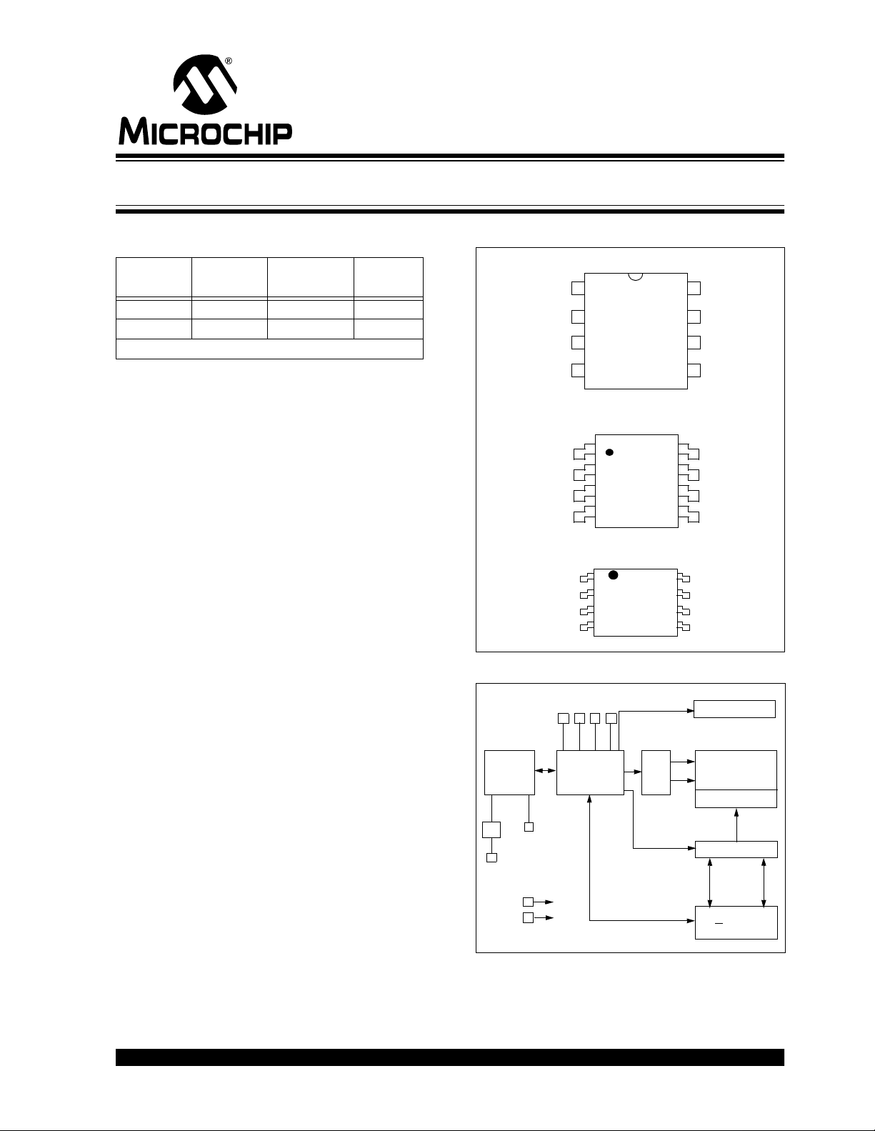
PACKAGE TYPE
8-LEAD PDIP
A0
1
A1
2
A2
3
4
Vss
8-LEAD SOIC
A0
A1
A2
Vss
8-LEAD TSSOP
WP
Vcc
A0
A1
1
2
3
4
1
2
3
4
BLOCK DIAGRAM
A0 A1 A2 WP
24xx64
24xx64
24xx64
8
7
6
5
8
7
6
5
8
7
6
5
Vcc
WP
SCL
SDA
Vcc
WP
SCL
SDA
SCL
SDA
Vss
A2
HV GENERATOR
DESCRIPTION
I/O
The Microchip Technology Inc. 24AA64/24LC64
(24xx64*) is a 8K x 8 (64K bit) Serial Electrically Eras-
CONTROL
LOGIC
able PROM capable of operation across a broad voltage range (1.8V to 5.5V). It has been developed for
advanced, low power applications such as personal
communications or data acquisition. This device also
has a page-write capability of up to 32 bytes of data.
This device is capable of both random and sequential
I/O
SDA
SCL
reads up to the 64K bound ary . Fu nctional addres s lines
allow up to eigh t devi ces on the s ame bus , for up to 51 2
Kbits address space. This device is available in the
VCC
VSS
standard 8-pin plastic DIP, 8-pin SOIC (150 and
208 mil), and 8-pin TSSOP.
2
I
C is a trademark of Philips Corporation.
*24xx64 is used in this document as a generic part number for the 24AA64/24LC64 devices.
2000 Microchip Technology Inc. DS21189D-page 1
MEMORY
CONTROL
LOGIC
XDEC
EEPROM
ARRAY
PAGE LATCHES
YDEC
SENSE AMP
R/W CONTROL
Page 2
24AA64/24LC64
1.0 ELECTRICAL CHARACTERISTICS
1.1 Maximum Ratings*
Vcc.................................................................................................7.0V
All inputs and outputs w.r.t. Vss .............................. -0.6V to Vcc +1.0V
Storage temperature ...................................................-65°C to +150°C
Ambient temp. with power applied ..............................-65°C to +125°C
Soldering temperature of leads (10 seconds) ........................... +300°C
ESD protection on all pins
*Notice: Stresses above those listed under “Maximum Ratings” may
cause permanent damage to the device. This is a stress rating only and
functional operation of the device at those or any other conditions
above those indicated in the operational listi ngs of this spe cificat ion is
not implied. Exposure to maximum rating conditions for extended periods may affect device reliability.
.................................................................≥ 4 kV
TABLE 1-1 PIN FUNCTION TABLE
Name Function
A0,A1,A2 User Confi gurable Chip Selects
SS Ground
V
SDA Serial Data
SCL Serial Clock
WP Write Protect Input
CC +1.8 to 5.5V (24AA64)
V
+2.5 to 5.5V (24LC64)
TABLE 1-2 DC CHARACTERISTICS
All parameters apply across the recommended opera ting ranges unless
otherwise noted.
Parameter Symbol Min Max Units Conditions
A0, A1, A2,
SCL, SDA, and WP pins:
High level input voltage V
Low level input voltage V
Hysteresis of Schmitt Trigger
inputs (SDA, SCL pins)
Low level output voltage V
Input leakage current I
Output leakage current ILO -10 10 µAVOUT = Vss to VCC
Pin capacitance
(all inputs/outputs)
Operating current I
Standby current I
Note: This parameter is periodically sampled and not 100% tested.
Commercial (C): VCC = +1.8V to 5.5V Tamb = 0°C to +70°C
Industrial (I): V
Automotive (E): V
IH 0.7 VCC — V
IL — 0.3 VCC
V
HYS 0.05 VCC — VVCC > 2.5V (Note)
OL — 0.40 V IOL = 3.0 mA @ VCC = 4.5V
LI -10 1 0 µAVIN = Vss to VCC, WP = VSS
CC = +2.5V to 5.5V Tamb = -40°C to +85°C
CC = +2.5V to 5.5V Tamb = -40°C to 125°C
VVVCC ≥ 2.5V
0.2 VCC
CC < 2.5V
V
OL = 2.1 mA @ VCC = 2.5V
I
VIN = Vss or VCC, WP = VCC
CIN, COUT — 10 pF VCC = 5.0V (Note)
Tamb = 25°C, f
CC Write — 3mAVCC = 5.5V
I
CC Read — 400 µA VCC = 5.5V, SCL = 400 kHz
CCS — 1 µA SCL = SDA = VCC = 5.5V
c
A0, A1, A2, WP = V
= 1 MHz
SS
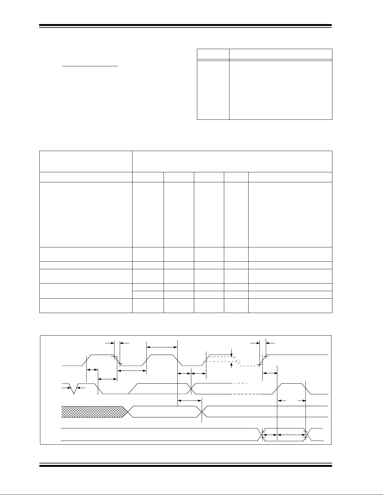
FIGURE 1-1: BUS TIMING DATA
TF
SCL
SDA
IN
SDA
OUT
WP
DS21189D-page 2 2000 Microchip Technology Inc.
TSU:STA
TSP
TLOW
THD:STA
THIGH
THD:DAT TSU:DAT TSU:STO
TAA
(protected)
(unprotected)
VHYS
TR
TSU:WP
TBUF
THD:WP
Page 3
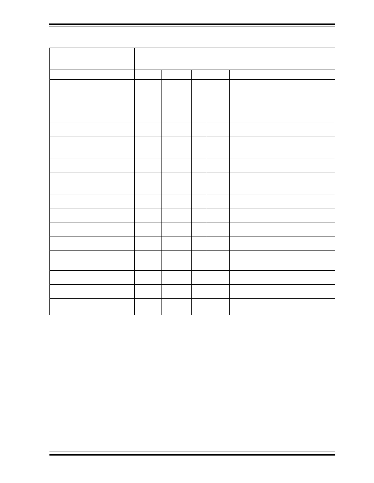
TABLE 1-3 AC CHARACTERISTICS
24AA64/24LC64
All parameters apply across the specified operating ranges unless otherwise noted.
Commercial (C): VCC = +1.8V to 5.5V Tamb = 0°C to +70°C
Industrial (I): V
Automotive (E): V
CC = +2.5V to 5.5V Tamb = -40°C to +85°C
CC = +2.5V to 5.5V Tamb = -40°C to 125°C
Parameter Symbol Min Max Units Conditions
Clock frequency F
Clock high time T
Clock low time T
SDA and SCL rise time
(Note 1)
SDA and SCL fall time T
START condition hold time T
START condition setup time T
Data input hold time T
Data input setup time T
STOP condition setup time T
WP setup time T
WP hold time T
HD:STA 4000
SU:STA 4700
HD:DAT 0 — ns (Note 2)
SU:DAT 250
SU:STO 4000
SU:WP 4000
HD:WP 4000
Output valid from clock
(Note 2)
Bus free time: Time the bus must be
T
free before a new transmission can
CLK —
—
HIGH 4000
600
LOW 4700
1300
R —
T
—
F — 300 ns (Note 1)
600
600
100
600
600
1300
AA —
T
—
BUF 4700
1300
100
400
—
—
—
—
1000
300
—
—
—
—
—
—
—
—
—
—
—
—
3500
900
—
—
kHz 1.8V ≤ VCC ≤ 2. 5V
≤ VCC ≤ 5.5V
2.5V
ns 1.8V ≤ VCC ≤ 2.5V
≤ VCC ≤ 5.5V
2.5V
ns 1.8V ≤ VCC ≤ 2.5V
≤ VCC ≤ 5.5V
2.5V
ns 1.8V ≤ VCC ≤ 2.5V
≤ VCC ≤ 5.5V
2.5V
ns 1.8V ≤ VCC ≤ 2.5V
≤ VCC ≤ 5.5V
2.5V
ns 1.8V ≤ VCC ≤ 2.5V
≤ VCC ≤ 5.5V
2.5V
ns 1.8V ≤ VCC ≤ 2.5V
≤ VCC ≤ 5.5V
2.5V
ns 1.8V ≤ VCC ≤ 2.5V
2.5V
≤ VCC ≤ 5.5V
ns 1.8V ≤ VCC ≤ 2.5V
≤ VCC ≤ 5.5V
2.5V
ns 1.8V ≤ VCC ≤ 2.5V
2.5V
≤ VCC ≤ 5.5V
ns 1.8V ≤ VCC ≤ 2.5V
2.5V
≤ VCC ≤ 5.5V
ns 1.8V ≤ VCC ≤ 2.5V
2.5V
≤ VCC ≤ 5.5V
start
Output fall time from V
IH
OF 10 250 ns C
T
≤ 100 pF (Note 1)
B
minimum to VIL maximum
Input filter spike suppression
SP — 50 ns (Notes 1 and 3)
T
(SDA and SCL pins)
Write cycle time (byte or page) T
Endurance 1M — cycles 25°C, V
Note 1: Not 100% tested. C
= total capacitance of one bus line in pF.
B
WC — 5
ms
CC = 5.0V, Block Mode (Note 4)
2: As a transmitter, the device must provide an internal minimum delay time to bridge the undefined region (minimum
300 ns) of the falling edge of SCL to avoid unintended generation of START or STOP conditions.
3: The combined TSP and VHYS specifications are due to new Schmitt trigger inputs which provide improved noise spike
suppression. This eliminates the need for a TI specification for standard operation.
4: This parameter is not tested but guaranteed by characterization. For endurance estimates in a specific application, please
consult the Total Endurance Model which can be obtained on Microchip’s BBS or website.
2000 Microchip Technology Inc. DS21189D-page 3
Page 4

24AA64/24LC64
2.0 PIN DESCRIPTIONS
2.1 A0, A1, A2 Chip Address Inputs
The A0,A1,A2 inputs are used by the 24xx64 for multiple device operation. The levels on these inputs are
compared with the corresponding bits in the slave
address. The chip is selected if the compare is true.
Up to eight de vic es may be connected to the same b us
by using different chip select bit combinations. These
inputs must be connected to either V
CC or VSS.
2.2 SDA Serial Data
This is a bi-directional pin used to transfer addresses
and data into and data out of the device. It is an opendrain terminal, therefore , the SDA b us requires a pullup
resistor to V
400 kHz)
For normal data transfe r SDA is allowed to ch ange only
during SCL low. Changes during SCL high are
reserved for indicating the START and STOP conditions.
CC (typical 10 kΩ for 100 kHz, 2 kΩ for
2.3 SCL Serial Clock
This input is us ed to synch roniz e th e dat a tr ansfer fro m
and to the device.
2.4 WP
This pin can be connected to either Vss, Vcc or left
floating. An internal pull-down resistor on this pin will
keep the device in the unprotected state if left floating.
If tied to Vss or left floating, normal memory operation
is enabled (read/write the entire memory 0000-1FFF).
If tied to V
operations are not affected.
CC, WRITE operations are inhibited. Read
3.0 FUNCTIONAL DESCRIPTION
The 24xx64 supports a bi-directional 2-wire bus and
data transmission protocol. A device that sends data
onto the bus is defined as a transmitter, and a device
receiving data as a receiver. The bus must be controlled by a master device which generates the serial
clock (SCL), controls the bus access, and generates
the START and STOP conditions while the 24xx64
works as a slave. Both master and slave can operate as
a transmitter or receiver but the master device determines which mode is activated .
4.0 BUS CHARACTERISTICS
The following bus protocol has been defined:
• Data transfer may be initiated only when the bus
is not busy.
• During data transfer, the data line must remain
stable whenever the clock line is H IG H. Chan ges
in the data line w hil e t he clo ck line is HIGH will be
interpreted as a START or STOP condition.
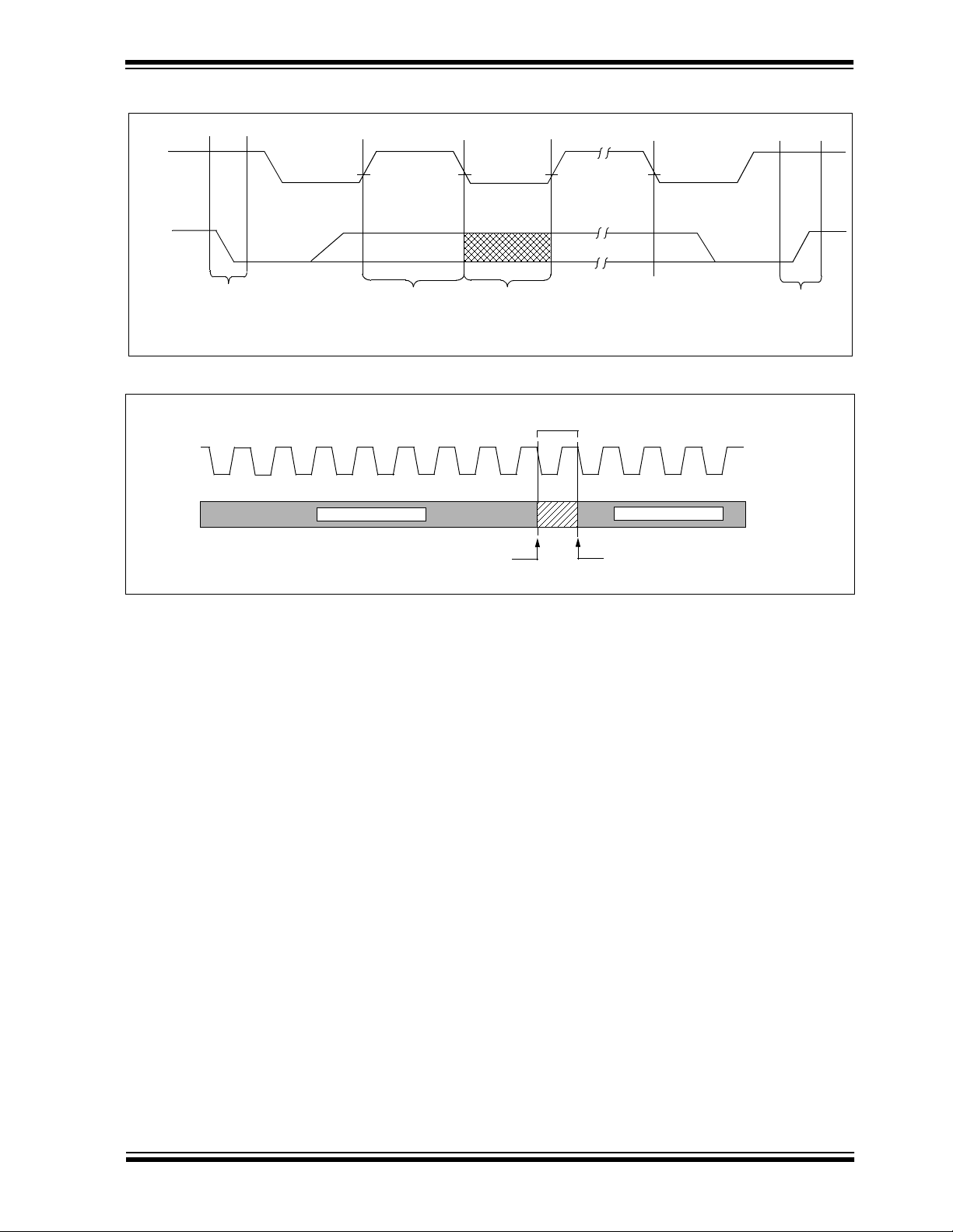
Accordingly, the following bus conditions have been
defined (Figure 4-1).
4.1 Bus not Busy (A)
Both data and clock lines remain HIGH.
4.2 Start Data Transfer (B)
A HIGH to LOW transition of the SDA line while the
clock (SCL) is HIG H determines a START condit ion. All
commands must be preceded b y a START condi tion .
4.3 Stop Data Transfer (C)
A LOW to HIGH transition of the SDA line while the
clock (SCL) is HI G H det ermines a S TOP cond iti on . All
operations must end with a STOP condition.
4.4 Data Valid (D)
The state of the data line represents valid data when,
after a START condition, the data line is stable for the
duration of the HIGH period of the clock signal.
The data on the line must be changed during the LOW
period of the cloc k si gnal. T here is on e clock pulse per
bit of data.
Each data transfer is initiated with a START condition
and terminated with a STOP condition. The number of
the data bytes transferred between the START and
STOP conditions is determined by the master device.
4.5 Acknowledge
Each receiving device, when addressed, is obliged to
generate an acknowledge signal after the reception of
each byte. The master device must generate an extra
clock pulse which is associated with this acknowledge
bit.
Note: The 24xx64 does not generate any
acknowledge bits if an internal programming cycle is in progress .
A device that acknowledges must pull down the SDA
line during the acknowledge clock pulse in such a way
that the SDA line is stable LOW during the H IGH period
of the acknowledge related clock pulse. Of course,
setup and hold times must be taken into account. During reads, a master must signal an end of data to the
slave b y NOT gener ating an acknowledg e bit on the last
byte that has be en clocke d out of the slav e. In thi s case,
the slave (24xx64) will leave the data line HIGH to
enable the master to generate the STOP condition.
DS21189D-page 4 2000 Microchip Technology Inc.
Page 5
24AA64/24LC64
FIGURE 4-1: DATA TRANSFER SEQUENCE ON THE SERIAL BUS
(A) (B) (D) (D) (C) (A)
SCL
SDA
START
CONDITION
ADDRESS OR
ACKNOWLEDGE
VALID
FIGURE 4-2: ACKNOWLEDGE TIMING
SCL
SDA
Transmitter must release the SDA line at this point
allowing the Receiver to pull the SDA line low to
acknowledge the previous eight bits of data.
Data from transmitter
DA TA
ALLOWED
TO CHANGE
Acknowledge
Bit
987654321 123
Data from transmitter
Receiver must release the SDA line at this point
so the Transmitter can continue sending data.
STOP
CONDITION
2000 Microchip Technology Inc. DS21189D-page 5
Page 6
24AA64/24LC64
5.0 DEVICE ADDRESSING
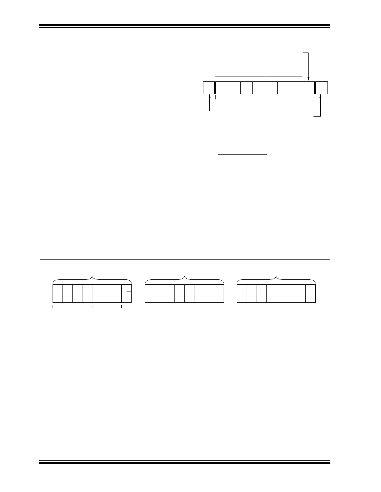
A control byte is the first byte received following the
start condition from t he master de vice (Figu re 5-1). The
control byte consists of a four bit control code; for the
24xx64 this is set as 1010 binary for read and write
operations. The next three bits of the control byte are
the chip sele ct bits (A2, A1 , A0). The chip select bits
allow the use of up to eight 24xx64 devices on the
same bus and are used to select which device is
accessed. Th e ch ip se lect b its in t h e con t rol byte must
correspond to the l ogic le v els on th e correspo nding A2,
A1, and A0 pi ns for t he device to respon d. Thes e bits
are in effect the three most signific ant bits of the word
address.
The last bit of the control byte defines the operation to
be performed. When set to a one a read operation is
selected, and when set to a zero a write operation is
selected. The next two bytes received define the
address of the first data byte (Figure 5-2). Because
only A12... A0 are used, the upper three address bits
are don’t care bits. The upper addre ss bits are t ransferred first, followed by the less significant bits.
Following the st ar t cond ition, t he 24xx 64 moni tors t he
SDA bus checking the device type identifier being
transmitted. Up on rece iving a 1010 co de and ap propriate device select bits, the slave device outputs an
acknowledge signal on the SDA line. Depending on the
state of the R/W
write operation.
bit, the 24xx64 will select a read or
FIGURE 5-1: CONTROL BYTE FORMAT
Read/Write Bit
Control Code
1 0 1 0 A2 A1 A0SACKR/W
Slave Address
Start Bit
Chip Select
Bits
Acknowledge Bit
5.1 Contiguous Addressing Across
Multiple Devices
The chip select bits A2, A1, A0 can be used to expand
the contiguous address space for up to 512K bits by
adding up to eight 24xx64's on the same bus. In this
case, software can use A0 of the control byte
address bit A13, A1 as address bit A14, and A2 as
address bit A15. It is not possible to sequentially read
across device boundaries.
as
FIGURE 5-2: ADDRESS SEQUENCE BIT ASSIGNMENTS
CONTROL BYTE ADDRESS HIGH BYTE ADDRESS LOW BYTE
1010
CONTROL
CODE
A2A1A
CHIP
SELECT
BITS
R/W XXX
0
A
12
A11A10A
A
8
9
A
••••••
7
X = Don’t Care Bit
A
0
DS21189D-page 6 2000 Microchip Technology Inc.
Page 7
24AA64/24LC64
6.0 WRITE OPERATIONS
6.1 Byte Write
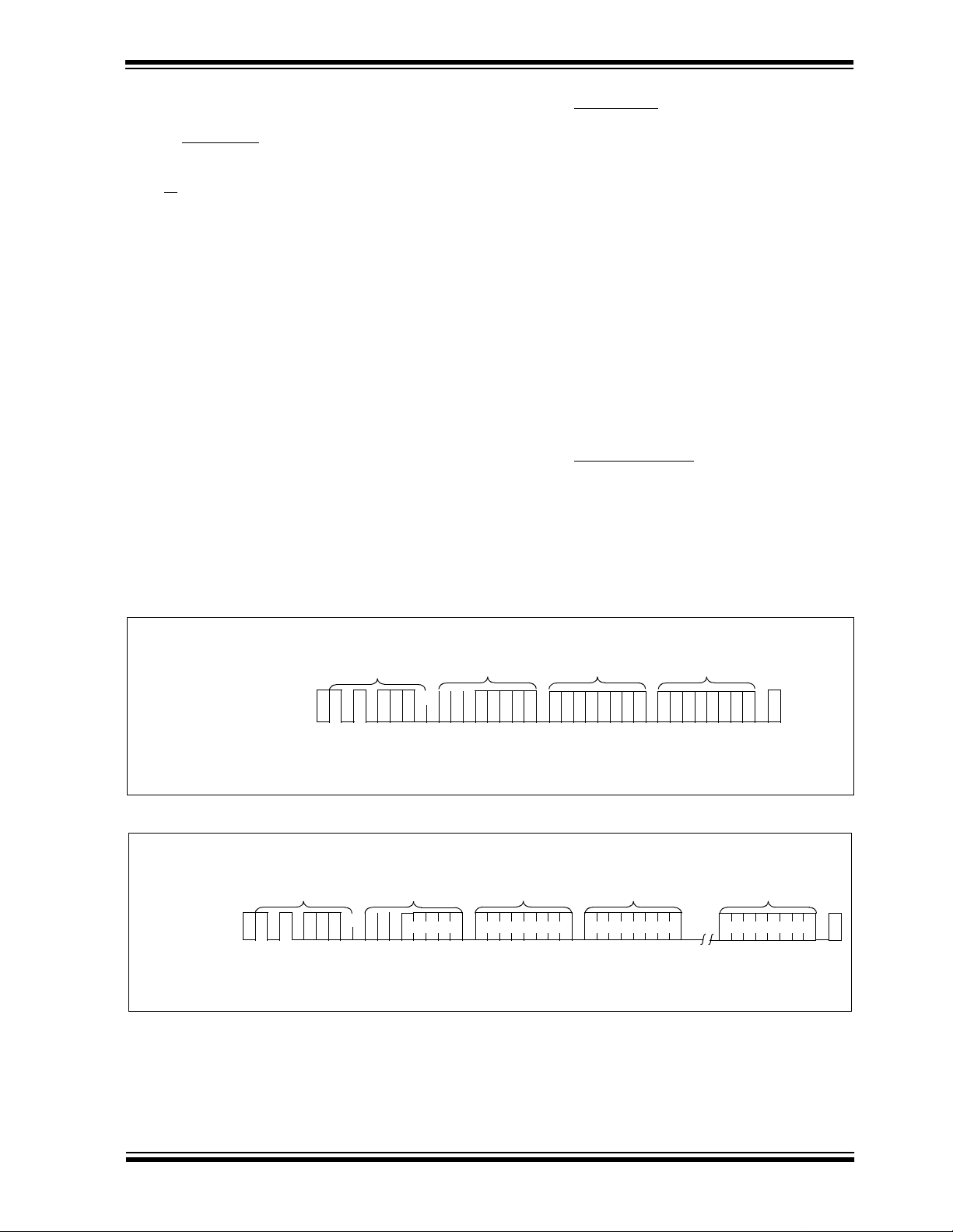
Following the start condition from the master, the
control code (fou r b its ), th e chi p sel ec t (t hree bits), and
the R/W
bus by the master transmitter. This indicates to the
addressed sla ve rec eiver that the addre ss high b yte will
follow after it has generated an acknowled ge b it d uring
the ninth clock cyc le . Therefore , the next byte transmitted by the master is the high-order byte of the word
address and will be written into the address pointer of
the 24xx64. The next byte is the least significant
address byte . After rece iving an other ac kno wledge si gnal from the 24xx64 the master device will transmit the
data word to be written into the addressed memory
location. The 24xx64 acknowledges again and the
master generates a stop condition. This initiates the
internal write cycle, a nd during t his time the 24xx64 w ill
not generate acknowledge signals (Figure 6-1). If an
attempt is made to write to the array with the WP pin
held high, the device will acknowledge the command
but no write cy cl e w i ll oc cu r, no data will be written and
the device will immediately accept a new command.
After a byte write command, the internal address
counter will point to the address location following the
one that was just wr itten.
bit (which is a logi c low) are clocked onto the
6.2 Page Write
The write control byte, word address and the first data
byte are transmitted to the 24xx64 in the same way as
in a byte write. But instead of generating a stop condition, the master transmits up to 31 additional bytes
which are tempor ari ly st ored in the on-chip page buffer
and will be written into me mory after th e master has
transmitted a sto p condition. After receipt of ea ch word,
the five lower address pointer bits are internally incremented by o ne. If the master shou ld trans mit more than
32 bytes prior to generating the stop condition, the
address counter will roll over and the previously
received data will be overwritten. As with the byte write
operation, on ce the stop condi tion i s rece ived, an internal write cycle will begin (Figure 6-2). If an attempt is
made to write to the arr ay with t he WP pin held h igh, the
device will acknowledge the command but no write
cycle will occur, no data will be written and the device
will immediately accept a new command.
6.3 Write Protection
The WP pin allows the user to write protect the entire
array (000 0-1F FF) whe n the pin is t ied to Vc c. If t ied to
SS or left floating, the write p rote ction is disa bl ed. Th e
V
WP pin is sampled at the ST OP bit for e v ery write command (Figure 1-1) T og gling the WP pin after the STOP
bit will hav e no effect on the ex ecution of the write cycl e.
FIGURE 6-1: BYTE WRITE
BUS ACTIVIT Y
MASTER
SDA LINE
BUS ACTIVIT Y
X = don’t care bit
S
T
A
R
T
S1010 0
FIGURE 6-2: PAGE WRITE
S
T
BUS ACTIVITY
MASTER
SDA LINE
BUS ACTIVITY
X = don’t care bit
CONTROL
A
R
T
S1010 0
BYTE
A2A1A
0
CONTROL
BYTE
A
2
ADDRESS
HIGH BYTE
XXX
A
C
K
A1A
ADDRESS
HIGH BYTE
XXX
0
A
C
K
ADDRESS
LOW BYTE DATA BYTE 0
A
C
K
A
C
K
ADDRESS
LOW BYTE
A
C
K
DATA
A
C
K
A
C
K
S
T
O
P
P
A
C
K
DATA BYTE 31
S
T
O
P
P
A
C
K
2000 Microchip Technology Inc. DS21189D-page 7
Page 8
24AA64/24LC64
7.0 ACKNOWLEDGE POLLING
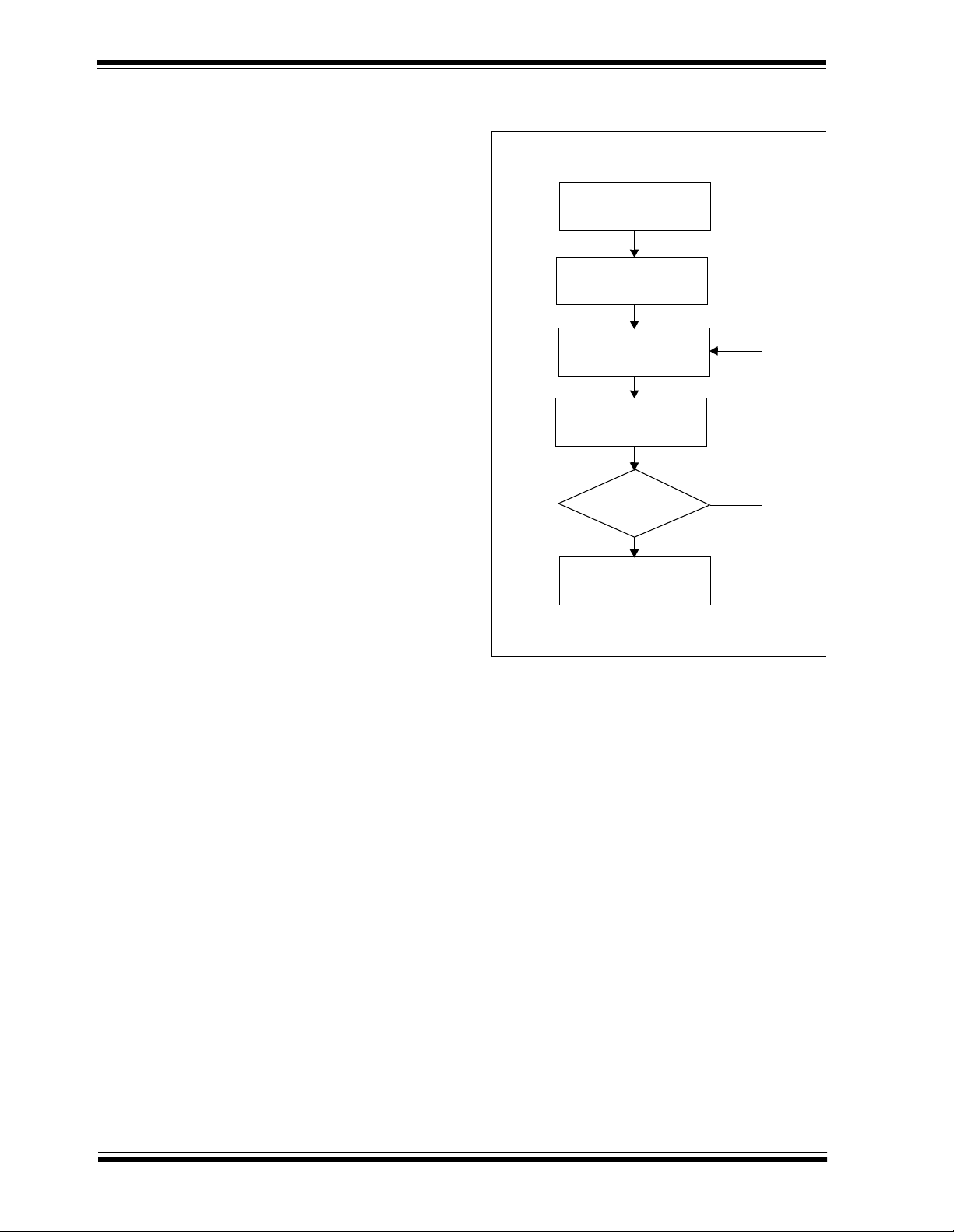
Since the device will not acknowledge during a write
cycle, this can be used to determine when the cycle is
complete (this feature can be used to maximize bus
throughput). Once the stop condition for a write command has been issued from the master, the device initiates the internally timed write cycle. ACK polling can
be initiated immedi ately. This invo lves t he master sending a star t cond ition fo llowed by the co ntrol byte fo r a
write command (R/W
the write cycle, then no A CK will be ret urned. If no AC K
is returned, then the start bit and control byte must be
re-sent. If the cycle is complete, then the device will
return the ACK and the master can then proceed with
the next read or write command. See Figure 7-1 for
flow diagram.
= 0). If the device is still busy with
FIGURE 7-1: ACKNOWLEDGE POLLING
FLOW
Send
Write Command
Send Stop
Condition to
Initiate Write Cycle
Send Start
Send Contr ol Byte
with R/W = 0
Did Device
Acknowledge
(ACK = 0)?
YES
NO
Next
Operation
DS21189D-page 8 2000 Microchip Technology Inc.
Page 9
24AA64/24LC64
8.0 READ OPERATION
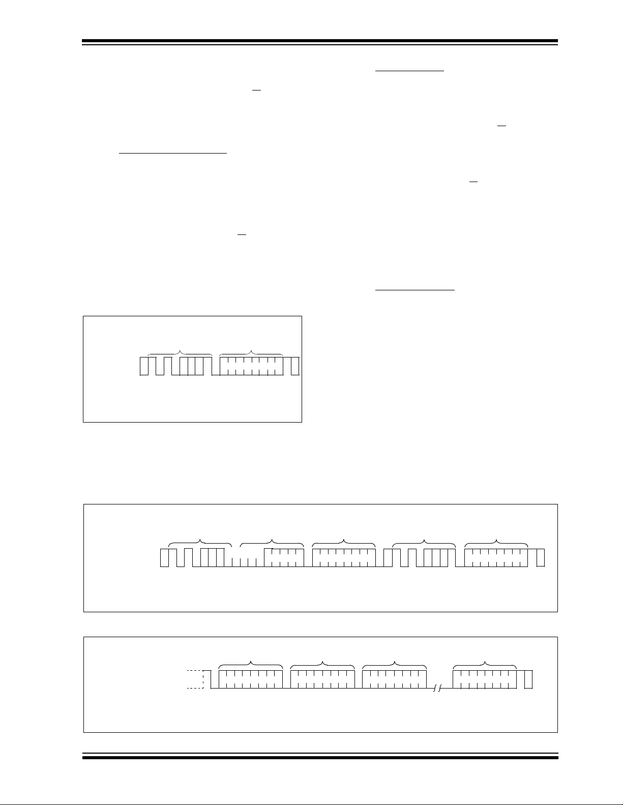
Read operations are initiated in the same way as write
operations with the exception that the R/W
control byte is set to one. There are three basic types
of read operations: current address read, random read,
and sequential read.
8.1 Current Address Read
The 24xx64 contains an address counter that maintains the address of the last word accessed, internally
incremented by one. Therefore, if the previous read
access was to address n (n is any legal address), the
next curren t address re ad opera tion w ould acce ss data
from address n + 1.
Upon receipt of the cont rol by te with R/W
the 24xx64 issues an acknowledge and transmits the
eight bit data word. The master will not acknowledge
the transfer b ut does gener a te a sto p cond ition a nd the
24xx64 discontinues transmission (Figure 8-1).
FIGURE 8-1: CURRE NT ADDRESS READ
S
BUS ACTIVITY
MASTER
SDA LINE
BUS ACTIVITY
T
CONTROL
A
R
T
S
1100
BYTE
AAA
210
1
A
C
K
bit of the
bit set to one,
DAT A
BYTE
N
O
A
C
K
S
T
O
P
P
8.2 Random Read
Random read operations allow the master to access
any memory location in a random manner. To perform
this type of read operation, first the word address must
be set. This is don e by sending the word address t o the
24xx64 as part of a write operation (R/W
bit set to 0).
After the word address is sent, the master generates a
start condition following the acknowledge. This terminates the write operation, but not before the internal
address pointer is set. Then the master issues the
control byte again b ut with the R/W
bit set to a one. The
24xx64 will then issue an acknowledge and transmit
the 8-bit data word. The master will not acknowledge
the transfer but does generate a stop condition which
causes the 24xx64 to discontinue transmission
(Figure 8-2). After a random read command, the internal address counter will point to the address location
following the one that was just read.
8.3 Sequential Read
Sequential reads are ini tiated in the same w ay as a ra ndom read except that after the 24xx64 transmits the
first data byte, the master issues an acknowledge as
opposed to the stop co nditi on us ed in a rand om re ad.
This acknowled ge directs the 24xx64 to transmit the
next sequentially addressed 8-bit word (Figure 8-3).
Following the final byte transmitted to the master, the
master will NO T gen erate an ack nowl edge b ut will generate a stop condition. To provide sequential reads the
24xx64 contains an internal address pointer which is
incremented by one at the completion of each operation. This address pointer allows the entire memory
contents to be serially read during one operation. The
internal address pointer w ill automa tically roll o ve r from
address 1FFF to address 0000 if the master acknowledges the byte received from the array address 1FFF.
FIGURE 8-2: RANDOM READ
BUS ACTIVITY
MASTER
SDA LINE
BUS ACTIVITY
X = Don’t Care Bit
S
T
A
CONTROL
R
BYTE
T
S1010
AAA
210
0
A
C
K
ADDRESS
HIGH BYTE
XXX
A
C
K
ADDRESS
LOW BYTE
S
T
A
R
T
S1010
A
C
K
CONTROL
BYTE
AAA
210
S
DATA
BYTE
1
A
C
K
T
O
P
P
N
O
A
C
K
FIGURE 8-3: SE QUENTIAL READ
BUS ACTIVITY
MASTER
SDA LINE
BUS ACTIVITY
2000 Microchip Technology Inc. DS21189D-page 9
CONTROL
BYTE
DATA n DATA n + 1 DATA n + 2 DATA n + X
A
C
K
A
C
K
A
C
K
A
C
K
S
T
O
P
P
N
O
A
C
K
Page 10

24AA64/24LC64
NOTES:
DS21189D-page 10 2000 Microchip Technology Inc.
Page 11
24AA64/24LC64
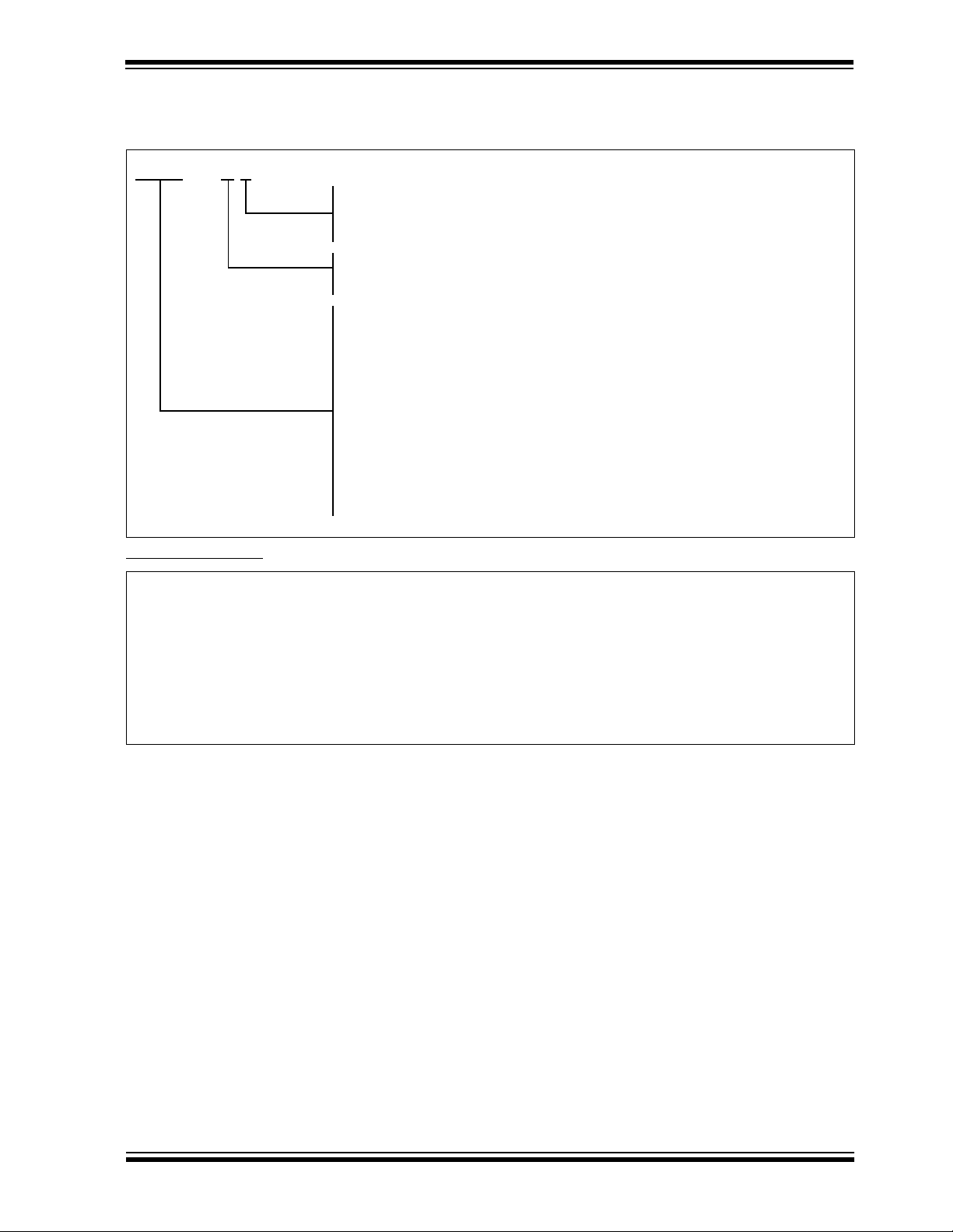
24xx64 PRODUCT IDENTIFICATION SYSTEM
To order or obtain information, e.g., on pricing or delivery, refer to the factory or the listed sales office.
24xx64 — /P
P = Plastic DIP (300 mil Body), 8-lead
Package:
Temperature
Range:
24AA64XT
Device:
24LC64XT
SN = Plastic SOIC (150 mil Body, EIAJ standard), 8-lead
SM = Plastic SOIC (208 mil Body, EIAJ standard), 8-lead
ST = TSSOP, 8-lead
Blank = 0°C to +70°C
I=-40°C to +85°C
E=-40°C to +125°C
24AA64
24AA64T
24AA64X
64K bit 1.8V I
64K bit 1.8V I
64K bit 1.8V I
in alternate pinout (ST only)
64K bit 1.8V I
2
C Serial EEPROM
2
C Serial EEPROM (Tape and Reel)
2
C Serial EEPROM
2
C Serial EEPROM
in alternate pinout (ST only)
24LC64
24LC64T
24LC64X
64K bit 2.5V I2C Serial EEPROM
64K bit 2.5V I
64K bit 2.5V I
in alternate pinout (ST only)
64K bit 2.5V I
2
C Serial EEPROM (Tape and Reel)
2
C Serial EEPROM
2
C Serial EEPROM
in alternate pinout (ST only)
Sales and Support
Data Sheets
Products supported by a preliminary Data Sheet may have an errata sheet describing minor operational differences and recommended workarounds. To determine if an errata sheet exists for a particular device, please contact one of the following:
1. Your local Microchip sales office
2. The Microchip Corporate Literature Center U.S. FAX: (480) 786-7277
3. The Microchip Worldwide Site (www.microchip.com)
Please specify which device, revision of silicon and Data Sheet (include Literature #) you are using.
New Customer Notification System
Register on our web site (www.microchip.com/ cn) to receive the most current information on our products.
2000 Microchip Technology Inc. DS21189D-page 11
Page 12
WORLDWIDE SALES AND SERVICE
AMERICAS
Corporate Office
Microchip Technology Inc.
2355 West Chandler Blvd.
Chandler, AZ 85224-6199
Tel: 480-786-7200 Fax: 480-786-7277
Technical Support: 480-786-7627
Web Address: http://www.microchip.com
Atlanta
Microchip Technology Inc.
500 Sugar Mill Road, Suite 200B
Atlanta, GA 30350
Tel: 770-640-0034 Fax: 770-640-0307
Boston
Microchip Technology Inc.
5 Mount Royal Avenue
Marlborough, MA 01752
Tel: 508-480-9990 Fax: 508-480-8575
Chicago
Microchip Technology Inc.
333 Pierce Road, Suite 180
Itasca, IL 60143
Tel: 630-285-0071 Fax: 630-285-0075
Dallas
Microchip Technology Inc.
4570 Westgrove Drive, Suite 160
Addison, TX 75248
Tel: 972-818-7423 Fax: 972-818-2924
Dayton
Microchip Technology Inc.
Two Prestige Place, Suite 150
Miamisburg, OH 45342
Tel: 937-291-1654 Fax: 937-291-9175
Detroit
Microchip Technology Inc.
Tri-Atria Office Building
32255 Northwestern Highway, Suite 190
Farmington Hills, MI 48334
Tel: 248-538-2250 Fax: 248-538-2260
Los Angel e s
Microchip Technology Inc.
18201 Von Karman, Suite 1090
Irvine, CA 92612
Tel: 949-263-1888 Fax: 949-263-1338
New York
Microchip Technology Inc.
150 Motor Parkway, Suite 202
Hauppauge, NY 11788
Tel: 631-273-5305 Fax: 631-273-5335
San Jose
Microchip Technology Inc.
2107 North First Street, Suite 590
San Jose, CA 95131
Tel: 408-436-7950 Fax: 408-436-7955
AMERICAS (continued)
Toronto
Microchip Technology Inc.
5925 Airport Road, Suite 200
Mississauga, Ontario L4V 1W1, Canada
Tel: 905-405-6279 Fax: 905-405-6253
ASIA/PACIFIC
Beijing
Microchip Technology, Beijing
Unit 915, 6 Chaoyangmen Bei Dajie
Dong Erhuan Road, Dongcheng District
New China Hong Kong Manhattan Building
Beijing 100027 PRC
Tel: 86-10-85282100 Fax: 86-10-85282104
Hong Kong
Microchip Asia Pacific
Unit 2101, Tower 2
Metroplaza
223 Hing Fong Road
Kwai Fong, N.T., Hong Kong
Tel: 852-2-401-1200 Fax: 852-2-401-3431
India
Microchip Technology Inc.
India Liaison Office
No. 6, Legacy, Convent Road
Bangalore 560 025, India
Tel: 91-80-229-0061 Fax: 91-80-229-0062
Japan
Microchip Technology Intl. Inc.
Benex S-1 6F
3-18-20, Shinyokohama
Kohoku-Ku, Yokohama-shi
Kanagawa 222-0033 Japan
Tel: 81-45-471- 6166 Fax: 81-45-471-6122
Korea
Microchip Technology Korea
168-1, Y oungbo Bldg. 3 Floor
Samsung-Dong, Kangnam-Ku
Seoul, Korea
Tel: 82-2-554-7200 Fax: 82-2-558-5934
Shanghai
Microchip Technology
Unit B701, Far East International Plaza,
No. 317, Xianxia Road
Shanghai, 200051 P.R.C
Tel: 86-21-6275-5700 Fax: 86-21-6275-5060
ASIA/PACIFIC (continued)
Singapore
Microchip Technology Singapore Pte Ltd.
200 Middle Road
#07-02 Prime Centre
Singapore 188980
Tel: 65-334-8870 Fax: 65-334-8850
Taiwan, R.O.C
Microchip Technology Taiwan
10F-1C 207
Tung Hua North Road
Taipei, Taiwan, ROC
Tel : 886 -2 -27 17- 71 75 Fax: 886-2-2545- 013 9
EUROPE
Denmark
Microchip Technology Denmark ApS
Regus Business Centre
Lautrup hoj 1-3
Ballerup DK- 2750 Denmark
Tel : 45 442 0 9895 Fax: 45 4420 9910
France
Arizona Microchip Technology SARL
Parc d’Activite du Moulin de Massy
43 Rue du Saule Trapu
Batiment A - ler Etage
91300 Massy, France
Tel: 33-1-69-53-63-20 Fax: 33-1-69-30-90-79
Germany
Arizona Microchip Technology GmbH
Gustav-Heinemann-Ring 125
D-81739 München, Germany
Tel: 49-89-627-144 0 Fax: 49-89-627-144-44
Italy
Arizona Microchip Technology SRL
Centro Direzionale Colleoni
Palazzo Taurus 1 V. Le Colleoni 1
20041 Agrate Brianza
Milan, Italy
Tel: 39-039-65791-1 Fax: 39-039-6899883
United Kingdom
Arizona Microchip Technology Ltd.
505 Eskdale Road
Winnersh Triangle
Wokingham
Berkshire, England RG41 5TU
Tel: 44 118 921 5858 Fax: 44-118 921-5835
01/05/00
Microchip received QS-9000 quality system
certification for its worldwide headquarters,
design and wafer fabrication facilities in
Chandler and Tempe, Arizona in July 1999. The
Company’s quality system processes and
procedures are QS-9000 compliant for its
PICmicro
devices, Serial EEPROMs and microperipheral
products. In addition, Microchip’s quality
system for the design and manufacture of
development systems is ISO 9001 certified.
®
8-bit MCUs, KEELOQ
®
code hopping
All rights reserved. © 2000 Microchip Technology Incorporated. Printed in the USA. 1/00 Printed on recycled paper.
Information contained in this publi c ation regarding device applications and the like is intended for suggestion only and may be superseded by updates. No representation or warranty is giv en and no liability is assumed
by Microchip T echnology Incorpora ted with respect to the accuracy or use of such information, or infringe ment of patents or othe r intellec tual property rights arising from such use or otherwis e. Use of Microchi p’s produc ts
as critical components in life s upport systems is not authorize d exc ept with express written appro val by M i crochip. No licenses are co nve yed, implicitly or otherwise, under any intellectual property rights. The Microchip
logo and name are registered trademarks of Mi crochip T echnology Inc. in the U.S.A. and other countries. All rights reserved. All other trademarks mentioned herein are the property of their respective companies.
DS21189D-page 12 2000 Microchip Technology Inc.
 Loading...