

Page 1

E
5 VOLT BOOT BLOCK FLASH MEMORY
n
High Performance Read
80/120 ns Max. Access Time
40 ns Max. Output Enable Time
n
Low Power Consumption
20 mA Typical Read Current
n
x8-Only Input/Output Architecture
Space-Constrained 8-bit
Applications
n
Optimized Array Blocking Architecture
One 16-KB Protected Boot Block
Two 8-KB Parameter Blocks
One 96-KB Main Block
One 128-KB Main Block
Top Boot Location
n
Hardware Data Protection Feature
Erase/Write Lockout during Power
Transitions
Absolute Hardware Protection for
Boot Block
n
Software EEPROM Emulation with
Parameter Blocks
28F002BC (x8)
n
n
n
n
n
n
n
n
n
PRELIMINARY
Extended Cycling Capability
100,000 Block Erase Cycles
Automated Byte Write and Block Erase
Industry-Standard Command User
Interface
Status Registers
Erase Suspend Capability
SRAM-Compatible Write Interface
Reset/Deep Power-Down Input
0.2 µA ICC Typical
Provides Reset for Boot Operations
Industry-Standard Surface Mount
Packaging
40-Lead TSOP
44-Lead PSOP
40-Lead PDIP
ETOX™ IV Flash Technology
5 V Read
12 V Write and Block Erase
VPP = 12 V ±5% Standard
VPP = 12 V ±10% Option
Independent Software Vendor Support
The Intel® 2-Mbit flash memory is an extension of the Boot Bloc k architec ture which i ncludes bl ock-selec tive
erasure, automated write and erase operati ons, and a standard microprocessor i nterface. The 2-Mbit flas h
memory enhances the Boot Block archi tecture by adding more density and blocks, x8 input/output c ontrol,
very high-speed, low-power, and industry-standard ROM-compatible pinout and surface mount packaging.
The Intel
selectable bus operation for 8-bit applications. The 28F002BC is a 2,097,152-bit nonvolatile memory
organized as 262,144 bytes of i nformation. It is of fered in 44-lead PSOP, 40-lead PDI P and 40-lead TSOP
package, which is ideal for space-constrained portable systems or any application with board space
limitations.
This device uses an int egrated Comm and User I nterf ace (CUI ) and Writ e S tat e M achi ne (WS M) for s impl ifi ed
byte write and block erasure. The 28F002BC provides block locations com patible with the Intel
family, 80286, 90860CA, and the Intel386™, Intel486™, Pentium
The boot block includes a data prot ection feature to protect the boot code in critical applications. Wi th a
maximum access time of 80 ns, t his high-performanc e 2-Mbit flas h memory interf aces at z ero wait-stat e to a
wide range of microprocessors and microcontroll ers. A deep power-down mode lowers the total V
consumption to 1 µW typic al. This power savings is critical in hand-held battery powered systems. For very
low-power applications using a 3.3 V supply, refer to the
datasheet (order number 290580). Manufact ured on Intel® 0.6 micron ETOX™ IV proces s technology, the
28F002BC flash memory provides world-class quality, reliability, and cost-effectiveness at the 2-Mbit density.
NOTE: This document formerly known as
®
28F002BC is an 8-bit wide flash mem ory offering. This high-dens ity flash memory provides user-
®
®
, and Pentium Pro microprocessors.
3 Volt Advanced Boot Block Flash Memory
28F002BC 2-Mbit (256K x 8) Boot Block Flash Memory
December 1998 Order Number: 290578-005
MCS®-186
power
CC
.
Page 2

Information in this document is provided in connection with Intel products. No license, express or implied, by estoppel or
otherwise, to any intellectual property rights is granted by this document. Except as provided in Intel’s Terms and Conditions of
Sale for such products, Intel assumes no liability whatsoever, and Intel disclaims any express or implied warranty, relating to
sale and/or use of Intel products including liability or warranties relating to fitness for a particular purpose, merchantability, or
infringement of any patent, copyright or other intellectual property right. Intel products are not intended for use in medical, life
saving, or life sustaining applications.
Intel may make changes to specifications and product descriptions at any time, without notice.
The 28F002BC may contain design defects or errors known as errata whic h may cause the product to deviate from published
specifications. Current characterized errata are available on request.
Contact your local Intel sales office or your distributor to obtain the latest specifications and before placing your product order.
Copies of documents which have an ordering number and are referenced in this document, or other Intel literature, may be
obtained from:
Intel Corporation
P.O. Box 5937
Denver, CO 80217-9808
or call 1-800-548-4725
or visit Intel’s website at http://www.intel.com
COPYRIGHT © INTEL CORPORATION 1996, 1997, 1998 CG-041493
*Third-party brands and names are the property of their respective owners.
Page 3

E 28F002BC
CONTENTS
PAGE PAGE
1.0 INTRODUCTION............................................. 5
1.1 Designing for Density Upgradeability........... 5
1.2 Main Features..............................................5
1.3 Applications................................................. 6
1.4 Pinouts ........................................................7
1.5 Pin Descriptions......................................... 10
2.0 PRODUCT DESCRIPTION ...........................11
2.1 Memory Organization ................................12
2.1.1 Blocking.............................................. 12
2.1.2 28F002BC-T Block Memory Map........ 12
3.0 PRINCIPLES OF OPERATION..................... 12
3.1 Bus Operations.......................................... 13
3.2 Read Operations........................................13
3.2.1 Read Array.......................................... 13
3.2.2 Intelligent Identifiers............................ 14
3.3 Write Operations........................................ 14
3.3.1 Command User Interface (CUI)........... 14
3.3.2 Status Register ................................... 17
3.3.3 Program Mode.................................... 17
3.3.4 Erase Mode ........................................ 18
3.3.5 Extended Cycling................................ 19
3.4 Boot Block Locking.................................... 19
3.4.1 V
3.4.2 RP# = V
= VIL for Complete Protection....... 19
PP
for Boot Block Unlocking... 19
HH
3.5 Power Consumption...................................23
3.5.1 Active Power....................................... 23
3.5.2 Standby Power....................................23
3.5.3 Deep Power-Down.............................. 23
3.6 Power-Up/Down Operation........................23
3.6.1 RP# Connected to System Reset........23
3.6.2 V
3.7 Power Supply Decoupling..........................24
3.7.1 V
4.0 ELECTRICAL SPECIFICATIONS.................25
4.1 Absolute Maximum Ratings ....................... 25
4.2 Operating Conditions.................................25
4.3 Capacitance...............................................25
4.4 DC Characteristics.....................................26
4.5 AC Characteristics—Read Only
4.6 AC Characteristics—WE#—Controlled Write
4.7 AC Characteristics—CE#—Controlled Write
4.8 Erase and Program Timings ...................... 35
5.0 ORDERING INFORMATION.........................35
6.0 ADDITIONAL INFORMATION.......................36
APPENDIX A: WSM Transition Table ............... 37
, VPP and RP# Transitions.............23
CC
Trace on Printed Circuit Boards....24
PP
Operations................................................ 29
Operations................................................ 30
Operations................................................ 33
PRELIMINARY
3
Page 4
28F002BC E
REVISION HISTORY
Date of
Revision
04/01/96 -001 Original version
09/01/96 -002 Pin 2 of 44-Lead PSOP changed from DU to NC
10/01/96 -003 40-Lead PDIP package added
12/01/97 -004
12/15/98 -005 Revised Section 1.1,
Version Description
Alternate program command (10H) removed
WSM transition table added
Erase Suspend/Resume Flowchart
V
and VPP ranges changed throughout document
CC
Pinouts
, to reflect current product offering.
Changed document title from
Flash Memory.
Designing for Density Upgradeability
changed
28F002BC 2-Mbit (256K x 8) Boot Block
, and 1.4,
4
PRELIMINARY
Page 5

E 28F002BC
1.0 INTRODUCTION
This datasheet comprises the specifications for
the 28F002BC 2-Mbit flash memory. Section 1.0
provides an overview of the 2-Mbit flash m emory,
including applications, pinouts, and pin
descriptions. Section 2.0 describes the memory
organization in detail. Section 3.0 defines a
description of the memory’s principles of
operation. Section 4.0 details the memory’s
operating specifications . Finally, Sections 5.0 and
6.0 provide ordering and reference information.
1.1 Designing for Density Upgradeability
The 28F002BC has been optimized to meet
market requirements. Applic ations currently using
the 28F001BX and 28F002BX can migrate to this
product. Of course, both the 28F001BX and the
28F002BX devices use an 8-bit wide bus . Those
applications needing a 16-bit bus can convert to
the 5 Volt Boot Block Flash memory 28F200B5,
28F400B5, 28F800B5 products. Low power
applications using a 3.3 V supply can convert to
the 3 Volt Advanced Boot Block Flash memory
family.
The 28F004B5 product is a natural migration path
to the 4-Mbit density. Both the 28F002BC and the
28F004B5 are offered in identical packages to
make upgrade seamless. A few simple
considerations can smooth the migration path
significantly:
1. Connect the NC pin of the 28F002BC to GND
(this will retain boot block locking when a
28F004B5 is inserted).
2. Design a switchable V
the 5 V V
3. If anticipating use of the 5 V V
switch V
protection.
Previous designs with Intel
occasion had to use a NOR gat e (or some other
scheme) to prevent issues with floating address es
latching incorrect data. The 28F002BC has
corrected this issue and does not need the NOR
gate. When migrating a design using the
option on the 28F004B5, device.
PP
to GND for complete write
PP
to take advantage of
PP
option,
PP
®
28F002BX devices on
28F002BX to the 28F002BC, the NOR gate can be
removed. When considering upgrading, packaging
is of paramount importance. Current and future
market trends indicate TSOP and PSOP as the
packages that will enable designs into the next
century.
1.2 Main Features
The 28F002BC Boot Block flas h memory is a highperformance, 2-Mbit (2,097,152 bi t) flash memory
organized as 256 Kbytes (262,144 bytes) of eight
bits each.
The 28F002BC has separately erasable blocks,
including a hardware-lockable boot block (16,384
bytes), two parameter blocks (8,192 bytes each)
and two main blocks (one block of 98,304 bytes
and one block of 131,072 bytes). An erase
operation typically erases one of the mai n blocks
in 2.4 seconds and the boot or paramet er blocks in
1.0 second. Each block can be independently
erased and programmed 100,000 times.
The boot block is located at the top of the address
map to match the protocol of many systems,
including the Intel
i860™ microprocessors as well as Pentium and
Pentium Pro microprocessors. The hardwarelockable boot block provides the mos t s ecure c ode
storage. The boot block is intended to store the
kernel code required for booting-up a system.
When the RP# pin is at V
unlocked and program and erase operations can
be performed. When the RP# pin is at V
boot block is locked and program and erase
operations to the boot block are ignored.
The Command User Interface (CUI) s erves as t he
interface between the microprocessor or
microcontroller and the internal operation of the
28F002BC.
Program and Erase Automation allows program
and erase operations to be executed using an
industry standard two-write c ommand sequenc e to
the CUI. Data writes are performed in byte
increments. Each by te in the f lash memory can be
programmed independently of other memory
locations but is erased simultaneously with all
other locations within the block.
®
MCS-186 family, 80960CA,
, the boot block is
HH
PPLK
, the
PRELIMINARY
5
Page 6
28F002BC E
Pentium®
Processor
100/90 MHz
Host
Bus
Main Memory
82430FX
PCIset
(82437FX)
Cache
PCI
Bus
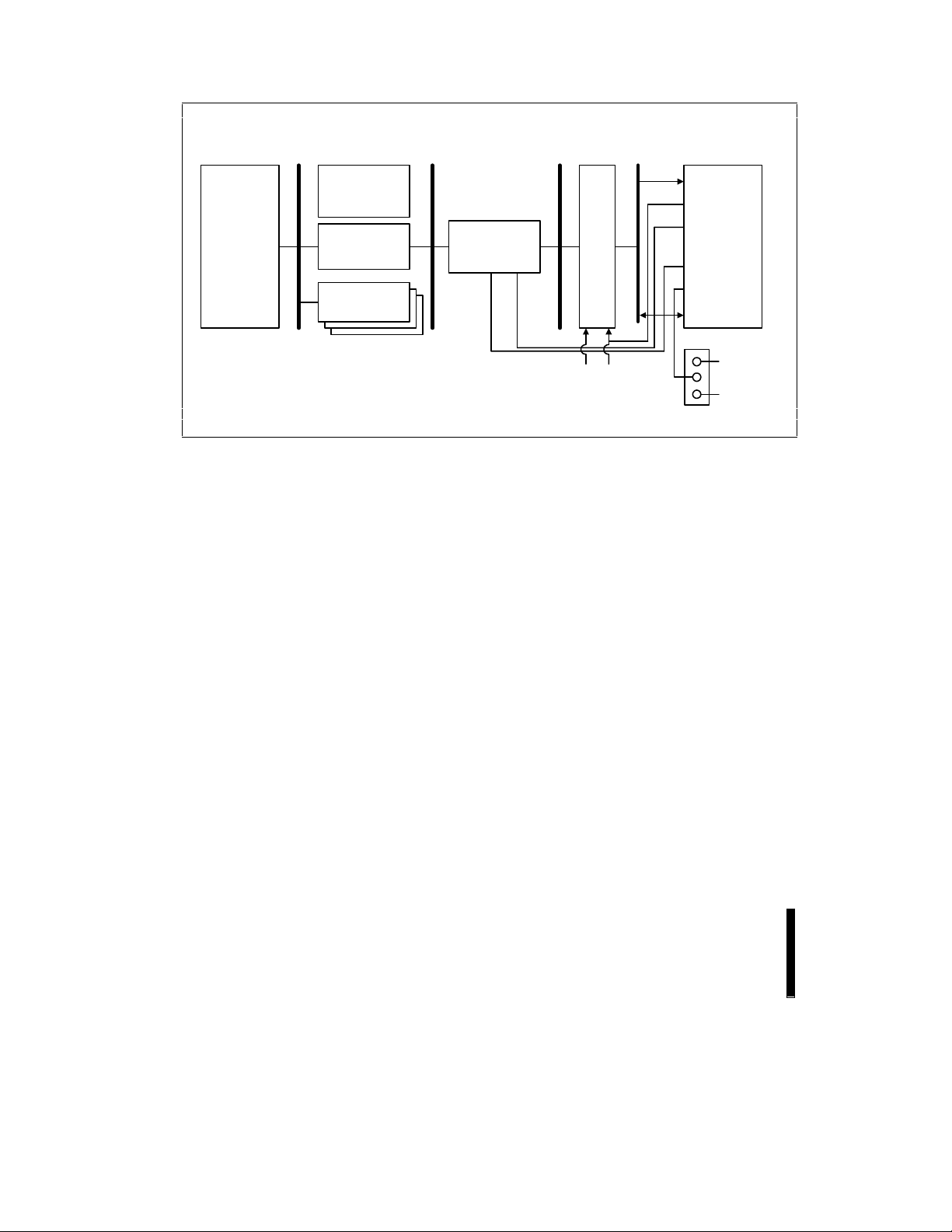
Figure 1. 28F002BC-T Interface to a Pentium® Microprocessor System
The Status Register (SR) indi cat es the s tat us of t he
internal Write State Mac hine (WSM), which reports
critical information on program and/or erase
sequences.
The maximum access time of 80 ns (t
ACC
) is
guaranteed over the commercial t emperature range
(0 °C to +70 °C), 10% V
(4.5 V to 5.5 V) and 100 pF output load. Ty pical I
active current is 20 mA.
supply voltage range
CC
CC
IPP, the maximum program current, is 20 mA. The
standard V
11.4 V to 12.6 V (V
voltage for erase and program is
PP
= 12 V ± 5%).
PP
The 28F002BC flash memory is als o designed wit h
a standby mode to minimiz e system current drain
and allow for low-power designs. When the CE#
and RP# pins are at V
is enabled and I
CC
, the CMOS standby mode
CC
drops to about 50 µA.
A deep power-down mode is enabled when the RP#
pin is at ground. In addition to minimizing power
consumption, the deep power-down mode also
provides write protection during power-up
conditions. I
mode is 0.20 µA typical . An init ial maxi mum ac cess
current during deep power-down
CC
time or reset time of 300 ns is required from RP#
switching high until output s are valid. Equivalently ,
the device has a maximum wake-up time of 215 ns
until writes to the CUI are recognized.
82430FX
PCIset
(82371FX)
XMEMW#
ISA
Bus
XMEMR#
XDOR
74S245
XOE#
BUFFER
X-Bus
A[16:0]
CE#
OE#
28F002BC
WE#
RP#
DQ[7:0]
When RP# is at ground, the WSM is reset, the
status register is cl eared, and the entire device is
write-protected. This feature prevents data
corruption and protects the code stored in the
device during system reset. The system Reset pin
can be tied to RP# to reset the memory to read
mode at power-up. With on-chip program/erase
automation and RP# functionality for data
protection, the device is protected against
unwanted program and/or erase cycles, even
during system reset.
1.3 Applications
2-Mbit Boot Block flash memory combines high
density, high performance, and cost-effective flash
memory with blocking and hardware protection
capabilities. Its flexibility and versatility reduces
cost throughout the product life cycle. Flash
memory is ideal for Just-In-Time production flow,
reducing system inventory and costs, and
eliminating component handling during the
production phase. During a product’s life cycle,
flash memory reduces costs by allowing userperformed code updates and feature enhancements
via floppy disk or remote link.
Intel®
PWROK
V
PP
0578_01
6
PRELIMINARY
Page 7
E 28F002BC
The 28F002BC is a full-function blocked flash
product suitable for a wide range of applications,
including extended PC BIOS, digital cellular phone
program and data storage, telecommunication
boot/firmware, and various embedded applications
where both program and data storage are required.
Reprogrammable systems, such as personal
computers, are ideal applications for the
28F002BC. Portable and hand-held personal
computer applications are bec oming more complex
with the addition of power management s oftware to
take advantage of the latest microprocessor
technology, the availability of ROM-based
application software, pen tablet c ode for electronic
handwriting, and diagnostic code. Figure 1 shows
an example 28F002BC application.
The increase in software sophistication augments
the probability that a code update will be required
after the PC is shipped. The 28F002BC provides a
safe and inexpensive update solution for desktop,
notebook, and hand-held personal computers while
extending the product lifetime. Furthermore, the
deep power-down mode provides added flexibility
for those battery-operated portable designs that
require low power.
A
16
A
15
A
14
A
13
A
12
A
11
A
9
A
8
WE#
RP#
V
PP
NC
NC
A
7
A
6
A
5
A
4
A
3
A
2
A
1
1
2
3
4
5
6
7
8
9
10
11
12
13
14
15
16
17
18
19
20
E28F002BC
Boot Block
40-Lead TSOP
10 mm x 20 mm
The 28F002BC is also an excellent design solution
for analog and digital cellular phone and
telecommunication switching applications requiring
high-performance, high-density storage in a small
form factor package (x8-only bus). The blocking
structure allows for easy segmentation of
embedded code for modular software designs. For
example, the parameter block can be used for
frequently updated data storage and diagnostic
messages (e.g., phone numbers and authorization
codes).
1.4 Pinouts
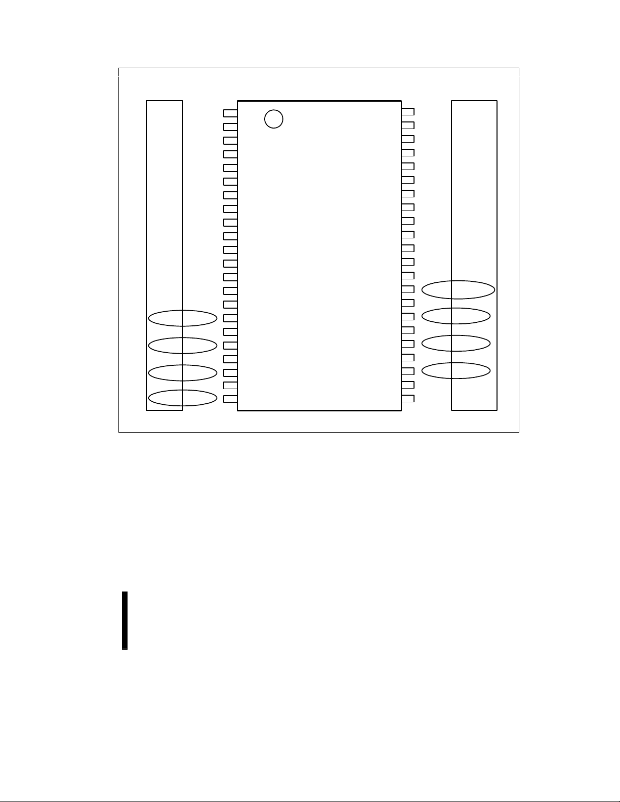
The 28F002BC in the 44-lead PSOP pinout fol lows
the industry-standard ROM/EPROM pinout, as
shown in Figure 4. The 28F200B5 pinout, indicating
the WP# input, is also s hown in the same diagram.
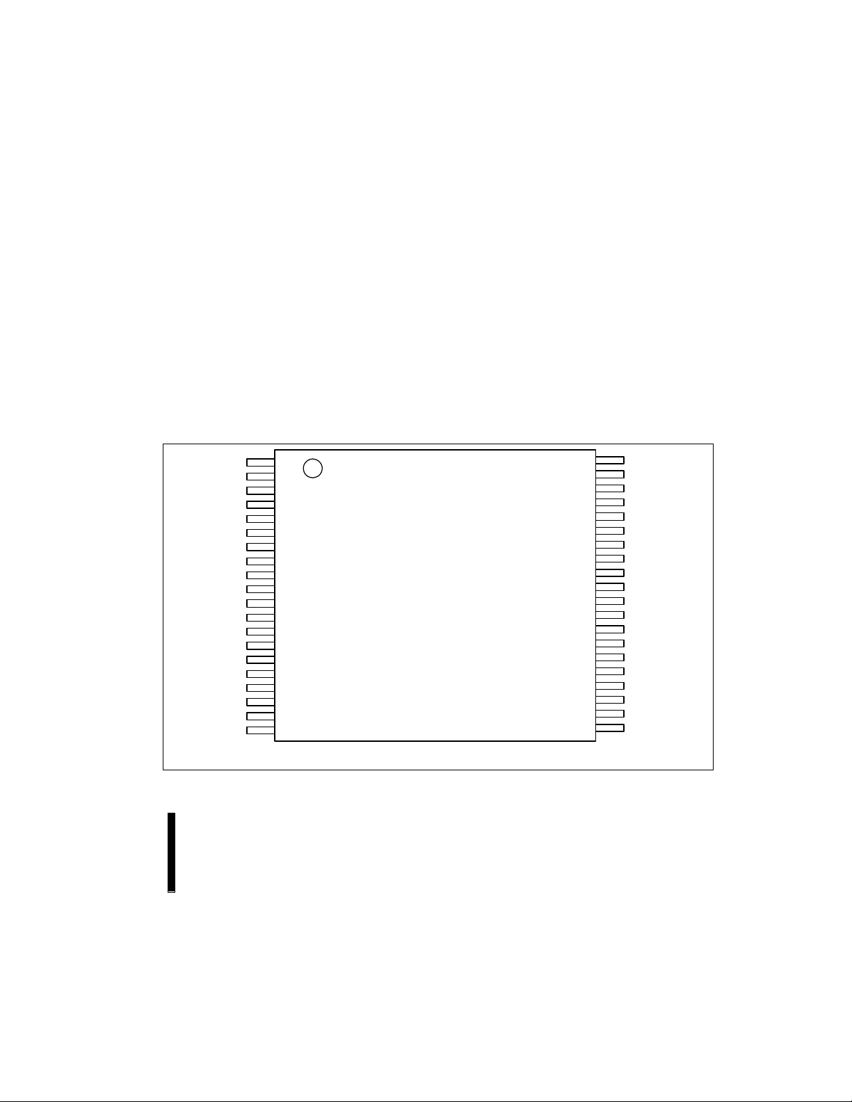
The 40-lead TSOP package (shown in Figure 2)
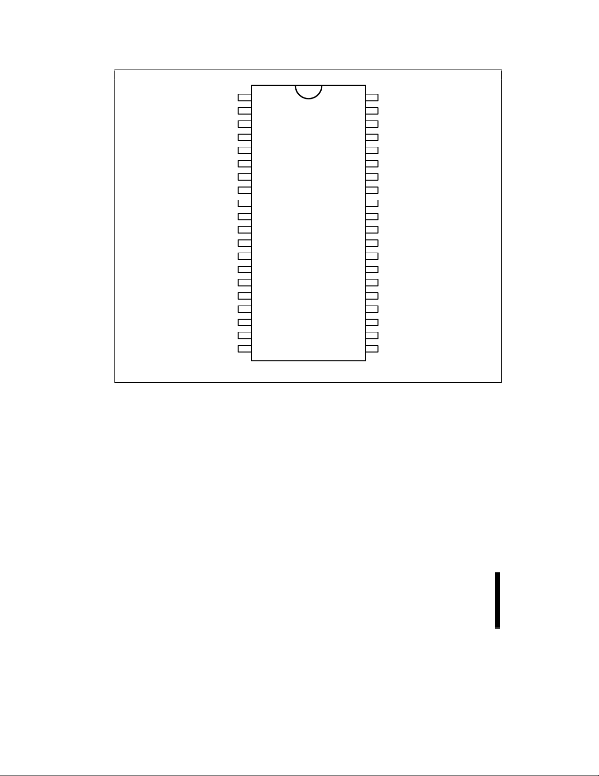
offers the smallest form factor possible. The lowcost 40-lead PDIP package diagram is shown in
Figure 3.
40
39
38
37
36
35
34
33
32
31
30
TOP VIEW
29
28
27
26
25
24
23
22
21
A
GND
NC
NC
A
DQ
DQ
DQ
DQ
V
V
NC
DQ
DQ
DQ
DQ
OE#
GND
CE#
A
17
10
7
6
5
4
CC
CC
3
2
1
0
0
0578_02
Figure 2. The 40-Lead TSOP Offers the Smallest Form Factor for Space-Constrained Applications
PRELIMINARY
7
Page 8
28F002BC E
NC
A
CE#
GND
OE#
DQ
DQ
DQ
DQ
V
CC
V
CC
DQ
DQ
DQ
DQ
A
10
GND
A
17
NC
1NC
2
0
3
4
5
6
0
1
2
3
7
8
9
10
11
P28F002BC
Boot Block
40-Lead PDIP
12
4
5
6
7
13
14
15
16
17
18
19
20
40
39
38
37
36
35
34
33
32
31
30
29
28
27
26
25
24
23
22
21
NC
A
A
A
A
A
A
A
V
PP
RP#
WE#
A
A
A
11
A
12
A
13
A
14
A
15
A
16
NC
1
2
3
4
5
6
7
8
9
0578_03
Figure 3. The 40-Lead PDIP Offers the Lowest Cost Package Solution
8
PRELIMINARY
Page 9
E 28F002BC
28F200B5 28F200B5
V
PP
WP#
NC
A
7
A
6
A
5
A
4
A
3
A
2
A
1
A
0
CE#
GND
OE#
DQ
DQ
DQ
DQ
DQ
DQ
10
DQ
DQ
11
V
PP
NC
NC
A
7
A
6
A
5
A
4
A
3
A
2
A
1
A
0
CE#
GND
OE#
DQ
NC
DQ
NC
DQ
0
1
2
0
8
1
9
2
NC
DQ
3
3
NC
10
11
12
13
14
15
16
17
18
19
20
21
22
1
2
3
4
5
6
7
8
9
PA28F002BC
Boot Block
44-Lead TSOP
0.525" x 1.110"
TOP VIEW
44
43
42
41
40
39
38
37
36
35
34
33
32
31
30
29
28
27
26
25
24
23
RP#
WE#
A
A
A
10
A
11
A
12
A
13
A
14
A
15
A
16
NC
GND
A
-1
DQ
NC
DQ
NC
DQ
NC
DQ
V
CC
RP#
WE#
8
9
A
8
A
9
A
10
A
11
A
12
A
13
A
14
A
15
A
16
NC
GND
DQ
15/A-1
DQ
7
6
5
4
DQ
DQ
DQ
DQ
DQ
DQ
V
7
14
6
13
5
12
4
CC
0578_04
Figure 4. The 44-Lead PSOP Offers a Convenient Upgrade from JEDEC ROM Standards
PRELIMINARY
9
Page 10

28F002BC E
1.5 Pin Descriptions
Table 1. 28F002BC Pin Descriptions
Symbol Type Name and Function
A–1,
A
–A
0
A
9
DQ0–
DQ
7
17
INPUT
INPUT ADDRESS INPUT: When A9 is at V
INPUT/
OUTPUT
CE# INPUT CHIP ENABLE: Activates the device’s control logic, input buffers, decoders and
OE# INPUT OUTPUT ENABLE: Enables the device’s outputs through the data buffers
WE# INPUT WRITE ENABLE: Controls writes to the command register and array blocks.
RP# INPUT RESET/DEEP POWER-DOWN: Provides three-state control. Puts the device in
V
CC
V
PP
GND GROUND: For all internal circuitry.
NC NO CONNECT: Pin may be driven or left floating.
ADDRESS INPUTS for memory addresses. Addresses are internally latched
during a write cycle. A
is used on the PSOP package only. A
-1
is used on the
17
TSOP and PDIP packages.
the signature mode is accessed. During
this mode, A
decodes between the manufacturer and device IDs.
0
HH,
DATA INPUTS/OUTPUTS: Inputs array data on the second CE# and WE#
cycle during a program operation. Inputs commands to the Command User
Interface when CE# and WE# are active. Data is internally latched during the
write cycle. Outputs array, intelligent identifier and status register data. The
data pins float to tri-state when the chip is de-selected or the outputs are
disabled.
sense amplifiers. CE# is active low. CE# high deselects the memory device and
reduces power consumption to standby levels. If CE# and RP# are high, but not
at a CMOS high level, the standby current will increase due to current flow
through the CE# and RP# input stages.
during a read cycle. OE# is active low.
WE# is active low. Addresses and data are latched on the rising edge of the
WE# pulse.
deep power-down mode, locks, and unlocks the boot block from program/erase.
When RP# is at logic high level (6.5 V maximum), the boot block is locked and
cannot be programmed or erased.
When RP# = V
programmed or erased.
(10.8 V minimum), the boot block is unlocked and can be
HH
When RP# is at a logic low level the boot block is locked, the deep power-down
mode is enabled and the WSM is reset—preventing any blocks from being
programmed or erased. When RP# transitions from logic low to logic high, the
flash memory enters the read array mode.
DEVICE POWER SUPPLY: 5.0 V ± 10%, 5.0 V ± 5%
PROGRAM/ERASE POWER SUPPLY: For erasing memory array blocks or
programming data in each block. When V
memory contents cannot be altered.
PP
< V
all blocks are locked and
PPLK
10
PRELIMINARY
Page 11
E 28F002BC
2.0 PRODUCT DESCRIPTION
DQ -DQ
07
A -A
0
Output
Buffer
Identifier
Register
Output
Power
Reduction
Control
17
Input
Buffer
Address
Latch
Address
Counter
Y-Decoder
X-Decoder
16-Kbyte
Boot Block
Multiplexer
8-Kbyte
Parameter Block
Status
Register
Data
Comparator
Y-Gating/Sensing
8-Kbyte
Parameter Block
Input
Buffer
I/O Logic
Data
Register
96-Kbyte
Main Block
128-Kbyte
Main Block
Command
User
Interface
Write State
Machine
Program/Erase
Voltage Switch
CE#
WE#
OE#
RP#
V
PP
V
GND
044819
CC
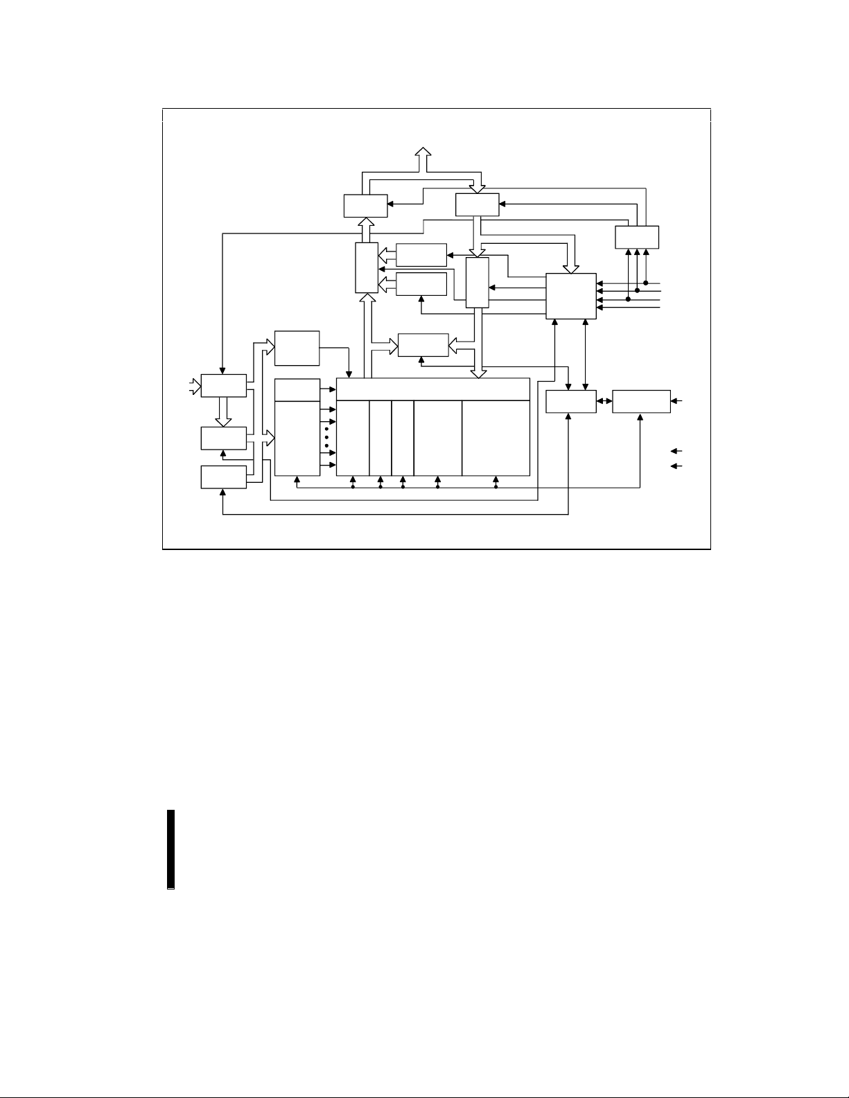
Figure 5. 28F002BC Internal Block Diagram
PRELIMINARY
11
Page 12

28F002BC E
2.1 Memory Organization
2.1.1 BLOCKING
The 28F002BC features an asymmetrical ly-blocked
architecture that provides system memory
integration. Each block can be erased up to
100,000 times. The block sizes have been chosen
to optimize their functionality for common
applications of nonvolat ile storage. For t he address
locations of the blocks, see the 28F002BC-T
Memory Map, Figure 6.
2.1.1.1 Boot Block - 16 KB
The boot block is intended to repl ace a dedicated
boot PROM in a microprocess or or microcontrollerbased system. The 16-Kbyte (16,384 bytes) boot
block is located at t he top of the address map as
shown in Figure 6. This boot block features
hardware controllable write-protection to protec t the
crucial microprocessor boot code from accidental
erasure. The boot block can be erased and written
when RP# is held at 12 V for the duration of the
erase or program operation. This feature allows
customers to change the boot code when
necessary while providing security at other times.
3FFFFH
3C000H
3BFFFH
3A000H
39FFFH
38000H
37FFFH
20000H
1FFFFH
00000H
Figure 6. 28F002BC-T Memory Map
16-Kbyte Boot Block
8-Kbyte Parameter Block
8-Kbyte Parameter Block
96-Kbyte Main Block
128-Kbyte Main Block
0578_06
2.1.1.2 Parameter Blocks - 8 KB (each)
The 28F002BC has two 8-Kbyte parameter blocks
to facilitate storage of frequently updated system
parameters that would normally require an
EEPROM. The parameter blocks can also be used
to store additional boot or main code. By using
software techniques, the byte-rewrite functionality
of EEPROMs can be emulated. These t echniques
are detailed in Intel’s applic ati on note
AP-604 Using
Intel’s Boot Block Flash Memory P arameter Blocks
to Replace EEPROM.
2.1.1.3 Main Block - 96 KB and 128 KB
The 28F002BC contains one 96-Kbyte (98,304
byte) block and one 128-Kbyte (131,072 byte)
block. These blocks are typically used for data or
code storage.
2.1.2 28F002BC-T BLOCK MEMORY MAP
The 16-Kbyte boot block of the 28F002BC-T is
located from 3C000H to 3FFFFH. The first 8-Kby te
parameter block resides in memory space from
3A000H to 3BFFFH. The second 8-Kbyte
parameter block consumes the memory area from
38000H to 39FFFH. The 96-Kbyte main block
extends from 20000H to 37FFFH, while the
128-Kbyte main block occupies the region from
00000H to 1FFFFH.
3.0 PRINCIPLES OF OPERATION
Flash memory improves upon EPROM capability
with in-circuit electrical write and erase. The Boot
Block flash memory utilizes a Command User
Interface (CUI) and automated algorithms to
simplify write and erase operations. The CUI allows
for 100% TTL-level control inputs, fixed power
supplies during erasure and programming, and
maximum EPROM compatibility.
When V
execute the following commands: Read Array,
Read Status Register, Clear Status Register, and
Intelligent Identifier. The device provides standard
EPROM read, standby and output disable
operations. Manufacturer identification and device
identification data c an be acc ess ed through t he CUI
or through the standard EPROM A
(V
High voltage on V
device. With V
< V
PP
) access for PROM programming equipment.
ID
, the device will only successfully
PPLK
high voltage
9
allows write and erase of the
PP
active, all functions associated
PP
12
PRELIMINARY
Page 13
E 28F002BC
with altering memory contents are accessible via
3.2.1 READ ARRAY
the CUI.
When RP# transitions from V
The purpose of the Write State Machine (WS M) is
to automate the write and erasure of the device
completely. The WSM will begin operation upon
receipt of a signal from the CUI and will report
device will be in read array mode and will respond
to the read control inputs (CE#, OE#, and address
inputs) without any comm ands being written to t he
CUI.
status back through the status regi st er. The CUI will
handle the WE# interface to the data and address
latches, as well as system software requests for
status while the WSM is in operation.
When the device is in read array mode, four control
signals must be manipulated to read data at the
outputs.
• WE# must be logic high (V
3.1 Bus Operations
Flash memory reads, erases and writes in-system
via the local CPU. All bus cycles to or from the flash
memory conform to standard microprocessor bus
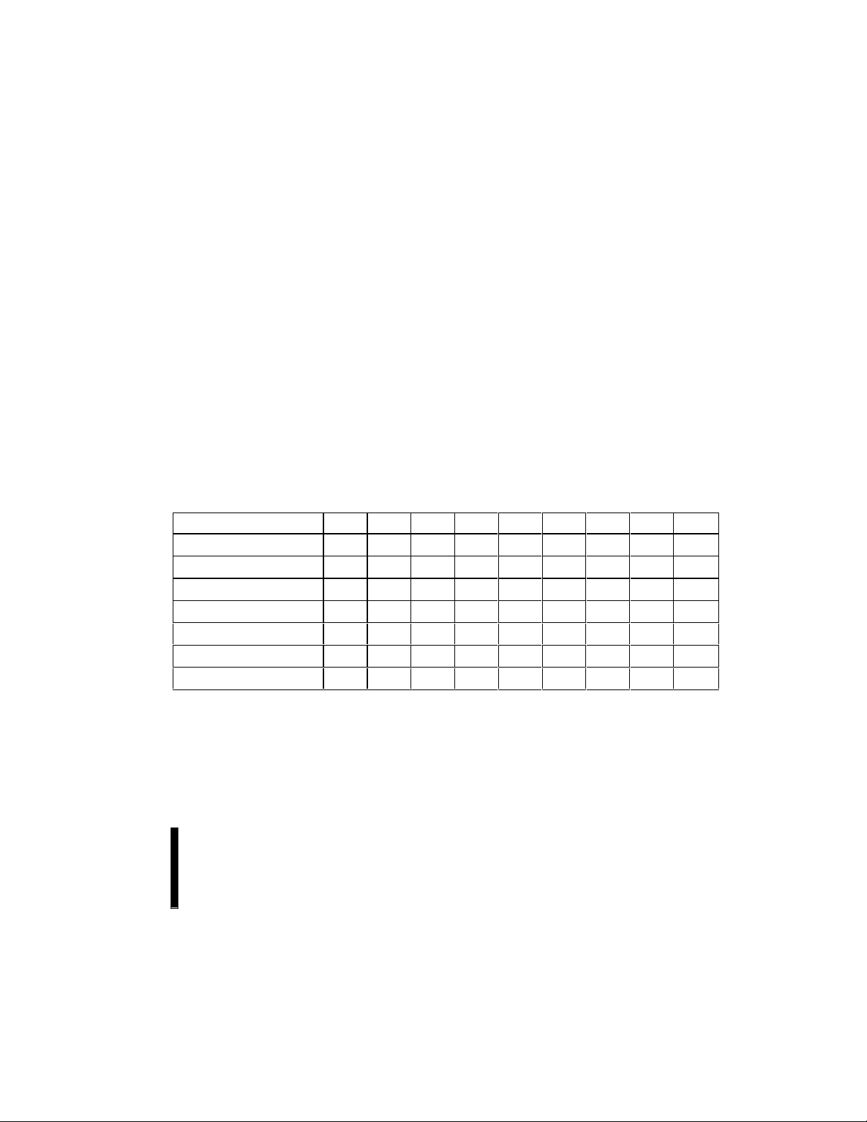
cycles. These bus operations are summarized in
Tables 2 and 4.
• CE# must be logic low (V
• OE# must be logic low (V
• RP# must be logic high (V
In addition, the address of the desired loc ati on mus t
be applied to the address pins. Refer to
Characteristics
for the exact sequence and timing
of these signals.
3.2 Read Operations
The 28F002BC has three user read modes: read
array, read intelligent identifier, and read status
register.
If the device is not in read array mode, as would be
the case after a program or erase operation, the
Read Mode command (FFH) must be written to t he
CUI before array reads can take place.
During power-up conditions, it t akes a maximum of
600 ns from when V
is at 4.5 V to when valid
CC
data is available at the outputs.
Table 2. 28F002BC Bus Operations
Mode Notes RP# CE# OE# WE# A
Read 1,2,3 V
Output Disable V
Standby V
Deep Power-Down 8 V
Intelligent Identifier (Mfr) 4 V
Intelligent Identifier (Device) 4 V
Write 5,6,7 V
NOTES:
1. Refer to
2. X can be V
3. See
4. Manufacturer and device codes may also be accessed via a CUI write sequence, A
5. Refer to Table 3 for valid D
6. Command writes for program or block erase are only executed when V
7. To write or erase the boot block, hold RP# at V
8. RP# must be at GND ± 0.2 V to meet the maximum deep power-down current specified.
DC Characteristics
, VIH for control pins and addresses, V
IL
DC Characteristics
.
for V
, V
PPH
, VHH, V
PPLK
during a write operation.
IN
IH
IH
IH
IL
IH
IH
IH
ID
HH
V
V
V
V
V
V
or V
PPLK
voltages.
.
V
IL
V
IL
IH
V
IL
V
IH
XXXD
IH
X X X High Z
IH
X X X X X High Z
X X X X X X High Z
V
IL
V
IL
V
IL
for VPP.
PPH
V
IL
V
IL
V
IH
= V
PP
V
IH
V
IH
XXV
IL
1-A17
.
PPH
PRELIMINARY
ID
ID
9
= X.
(reset) to VIH, the
IL
)
IH
)
IL
)
IL
)
IH
A
V
0
PP
V
V
IL
IH
X 89H
X 7CH
PPH
DQ
OUT
D
AC
0–7
IN
13
Page 14

28F002BC E
3.2.2 INTELLIGENT IDENTIFIERS
The manufacturer and device codes are read via
the CUI or by taking t he A
pin to VID. Writing 90H
9
to the CUI places the device into Intelligent
Identifier read mode. A read of location 00000H
outputs the manufacturer’s i dentificat ion code, 89H.
Reading location 00001H outputs the device ID,
7CH.
The 28F002BC device ID of 7CH is identic al to the
E28F002BX (40-lead TSOP). It differs from the
PA28F200BX (44-lead PSOP), which has a device
ID of 2274H. Designers using the PA28F200BX in
the x8 mode who wish to migrate to the
PA28F002BC need to be mindful of thi s device ID
difference and modify software drivers as
necessary. The 40-lead PDIP device ID is 7CH.
3.3 Write Operations
There are two commands that alter memory array
contents: Program Set up and Erase S etup/Conf irm.
In addition, the Erase Sus pend com mand sus pends
the WSM during an erase operation and releases
the CUI to accept any Read command (so long as it
is to a block other than the one being erased).
Finally, there is a Clear Status Register c ommand
for resetting the content s of the st atus regist er. This
command should be invoked following all
operations that modify the status register.
All commands written to the CUI will be interpreted,
but for any write operation to be ini tiated, the V
voltage must be at VHH. Depending on the
application, the design may hav e a switchable V
power supply or the VPP may be “hard-wired” to
12 V. The 28F002BC will function normally in either
case. It is highly recommended that RP# is tied to
the system RESET for data protection during
unstable CPU reset and also for proper CPU / flash
synchronization.
Furthermore, when attempting to modify the
contents of the 28F002BC’s boot block area, V
must be applied to both VPP and RP# for the
operation to be valid. Whether attempting to alter
the contents of the boot bl ock or any other memory
array area, if the proper voltages are not applied to
the correct input signals the write operation will be
aborted. Subsequently, the status register will
respond with either Bit 3 (V
low error), Bit 4
PP
(program error) or Bit 5 (erase error) being set (refer
to Table 5 for status register definitions).
HH
3.3.1 COMMAND USER INTERFACE (CUI)
The Command User Interface (CUI) s erves as the
interface between the microprocessor and the
internal chip controller. Commands are written to
the CUI using standard microprocessor write
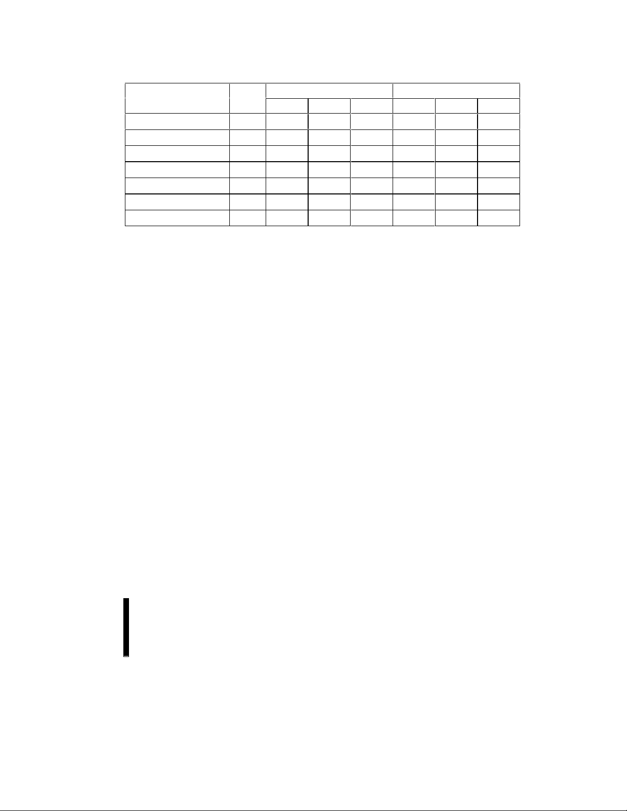
timings. The available commands (summarized in
Tables 3 and 4) are Read Array, Read Intelligent
Identifier, Read Status Register, Clear Status
Register, Program Setup, Erase Setup/Confirm,
and Erase Suspend.
For Read commands, the CUI points the read path
at either the array, the intelligent identifier, or the
status register depending on the command
received. For Program or Erase commands, the
CUI informs the Write St ate Machine (WSM) that a
Program or Erase has been requested. During the
execution of a Program command, the WSM
controls the programming sequences and the CUI
responds only to status register reads. During an
erase cycle, the CUI responds only to status
register reads and Erase Suspend. After the WSM
has completed its task, it will set the WSM Status
bit (bit 7 of the status register) to a “1,” which will
also allow the CUI to respond to its f ull command
set. Note that after the WSM has returned c ontrol to
the CUI, the CUI will stay in t he read status register
mode until it receives another command (see
Appendix A).
Table 3. Command Set Codes and
Corresponding Device Mode
PP
PP
Command Codes Device Mode
00 Invalid/Reserved
20 Erase Setup
40 Program Setup
50 Clear Status Register
70 Read Status Register
90 Intelligent Identifier
B0 Erase Suspend
D0 Erase Resume/Erase Confirm
FF Read Array
14
PRELIMINARY
Page 15
E 28F002BC
Table 4. Command Bus Definitions
First Bus Cycle Second Bus Cycle
Command Notes Oper Addr Data Oper Addr Data
Read Array Write X FFH
Intelligent Identifier 1,2 Write X 90H Read IA IID
Read Status Register Write X 70H Read X SRD
Clear Status Register Write X 50H
Program Setup Write PA 40H Write PA PD
Block Erase/Confirm Write BA 20H Write BA D0H
Erase Suspend/Resume Write X B0H Write X D0H
ADDRESS DATA
BA = Block Address SRD = Status Register Data
IA = Identifier Address IID = Intelligent Identifier Data
PA = Program Address PD = Program Data
X = Don’t Care
NOTES:
1. Bus operations are defined in Table 2.
2. Following the Intelligent Identifier command, two read operations access manufacturer and device codes respectively.
3.3.1.1 Command Function Description
Device operations are selected by writing specific
commands into the CUI. Tabl es 3 and 4 define t he
available commands. Status register (SR) bits are
defined in Table 5.
Invalid/Reserved
These are unassigned commands and should not
be used. Intel reserves the right to redefine these
codes for future functions.
Read Array (FFH)
This single write cycle command points the read
path at the array. If the host CPU performs a
CE#/OE#-controlled Read immediately following a
two-write sequence (i.e., a Program or Erase
command) that started the WSM, then the device
PRELIMINARY
will output status register contents. Writing two
Read Array (FFH) commands to the CUI aborts the
current operation and resets to read array mode.
Executing Read Array after the Erase Setup
command (instead of giving Erase Conf irm) causes
the status register eras e and program s tatus bi ts to
be set. This indicates that an erase operation was
initiated but not successfully confirmed (an Erase
Confirm at this point would be ignored by the CUI).
A subsequent Read Array command will point the
data path at the array (see Appendix A).
Intelligent Identifier (90H)
After this command is exec uted, the CUI points the
output path to the intelligent identifier circuits . Only
intelligent identifier values at addresses 0 and 1 can
be read (only address A
other address inputs are ignored).
is used in this mode; all
0
15
Page 16

28F002BC E
Read Status Register (70H)
This is one of three commands that is executable
while the WSM is operating. After this command is
written, a read of the device will output the c ontents
of the status register, regardless of the address
presented to the device. The device automatically
enters this mode after program or erase has
completed.
Clear Status Register (50H)
The WSM can set the program status and erase
status bits in t he status register t o “1,” but it cannot
clear them to “0.”
The status register is operated in this fashion for
two reasons, the first is synchroni zation. Since the
WSM does not know when the host CPU has read
the status register, it would not know when to cl ear
the status bits. Second, if the CPU is programming
a string of bytes, i t may be more efficient to query
the status register after programming the string.
Thus, if any errors exist while programming the
string, the status register will return the
accumulated error status. The Clear Status
Register command clears t he program, erase, and
status bits to “0.”
V
PP
Program Setup (40H)
This command simply sets the CUI into a state
such that the next write will load the Address and
Data registers. After this command is ex ecuted, the
outputs default to the status register. Two
consecutive Read Array commands (FFH) are
required to reset to Read Array after the Program
Setup command.
Program
The write following the Program Setup command
will latch address and data. Also, the CUI initiates
the WSM to begin execution of the program
algorithm. The device outputs status register data
when OE# is enabled. To read array data after the
program operation is completed, a Read Array
command is required.
Erase Setup (20H)
The Erase Setup command prepares the CUI for
the Erase Confirm command. No other action is
taken. If the next c omm and is not an E rase Confi rm
command, then the CUI will set both the program
status and erase stat us bits of the status regis ter t o
a “1,” place the device into read status register
mode, and wait for another command.
Erase Confirm (D0H)
If the previous command was an Erase Setup
command, then the CUI will enable the WSM to
erase, at the same time closing the address and
data latches, and respond only to t he Read Status
Register and Erase Suspend commands . While the
WSM is executing, the device will output status
register data when OE# is toggled low. Status
register data can only be updat ed by toggling either
OE# or CE#. If the previous command was not t he
Erase Setup command (20H), the Erase Confirm
command is ignored. Status register bits 4 and 5
are both set to indicate an invalid command
sequence.
Erase Suspend (B0H)
This command is only valid while the WSM is
executing an erase operation. At all other times,
this command is ignored. After this command has
been executed, the CUI will set a s ignal that direct s
the WSM to suspend erase operations. While
waiting for the erase to be suspended, the CUI
responds only to the Read Status Register
command or to the Erase Resume command. Once
the WSM has reached the Suspend stat e, it will set
an output in the CUI that allows the CUI to respond
to the Read Array, Read Status Register, and Erase
Resume commands. In this mode, the CUI will not
respond to any other commands. The WSM will
also set the WSM and erase s uspend stat us bits to
a “1.” The WSM will continue to run, idling in the
Suspend state, regardless of t he state of all input
control pins except V
below V
, the VPP low status bit (SR.3) will be
PPLK
and RP#. If VPP is taken
PP
set and the WSM will abort the suspended erase
operation. If active, RP# will immediately s hut down
the WSM and the remainder of the chip. During a
suspend operation, the data and address latches
will remain closed, but the address pads are able to
drive the address into the read path.
16
PRELIMINARY
Page 17

E 28F002BC
Erase Resume (D0H)
This command will cause the CUI to clear the
Suspend state and clear the WSM status bit to a
“0,” but only if an Erase Suspend command was
previously issued. Erase Resume will not have any
effect under any other conditions.
3.3.2 STATUS REGISTER
The 28F002BC contains a status register which
may be read to determine when a program or erase
operation is complete, and whether that operation
completed success fully. The s tatus regis ter may be
read at any time by writing the Read Status
Register command to the CUI. After writing this
command, all subsequent read operations output
data from the status regis ter unt il another c ommand
is written to the CUI. A Read Array c ommand must
be written to the CUI to return t o read array mode.
The status register bits are output on DQ[0:7] . The
contents of the status register are latched on
the falling edge of OE# or CE#, whichever
occurs last in the read cycle. This prevents
possible bus errors that mi ght occur if the contents
of the status register change while reading the
status register. CE # or OE# must be toggled with
each subsequent status read to insure the status
register is updated; otherwis e, the completion of a
program or erase operation will not be evident from
the status register.
When the WSM is active, the status register will
indicate the status of the WSM and upon c ommand
completion, it will indicate success or failure of the
operation (see Table 5 for definition of status
register bits).
written to the CUI. Then, any other command may
be issued to the CUI. Note, again, that before a
read cycle can be initiated, a valid read command
must be written to the CUI to specify whether the
read data is to come from the m emory array, status
register, or intelligent identifier.
3.3.3 PROGRAM MODE
Programming is executed using a two-write
sequence. The Program Setup command is writ ten
to the CUI followed by a second write which
specifies the address and data to be programmed.
The WSM then executes a s equence of internally-
timed events to:
1. Program the desired bits of the addressed
memory byte.
2. Verify that the desired bits are sufficiently
programmed.
Programming of the memory res ults in spec ific bits
within a byte being changed to a “0.”
If the user attempts to program “1”s, there will be no
change in memory contents and no error is reported
by the status register.
Similar to erasure, the status register indicates
whether programming is complete. While the
program sequence is executing, bit 7 of the s tatus
register is a “0.” The status register can be polled
by toggling either CE# or OE# to determine when
the program sequence is complet e. Only the Read
Status Register command is valid while
programming is active.
3.3.2.1 Clearing the Status Register
The WSM sets status bit s “3” t hrough “7” to “1,” and
clears bits “6” and “7” to “0,” but cannot clear status
bits “3” through “5” to “0.” Bits 3 through 5 can only
be cleared by the controlling CPU through the use
of the Clear Status Regist er command. These bits
can indicate various error conditions. By allowing
the system software to control the resetting of these
bits, several operations may be perform ed (such as
cumulatively programm ing several bytes or erasing
multiple blocks in sequence). The status register
may then be read to determine if an error occurred
during that programming or erasure series. This
feature adds flexibility to the way t he devic e may be
programmed or erased. To clear the status regis ter,
the Clear Status Register command is
PRELIMINARY
When programming is complete, the status bits,
which indicate whether the program operation was
successful, s hould be checked. If t he programming
operation was unsuccessful, bit 4 of the status
register is set to a “1” t o indicate a program failure.
If bit 3 is set to a “1,” then V
acceptable limits, and the WSM di d not execut e the
programming sequence. If the program operation
fails, bit 4 of the status register will be set within
1.5 ms, as determined by the timeout of the WSM.
The status register should be cleared before
attempting the next operat ion. Any CUI instruction
can follow after programming is completed;
however, reads from the memory array c annot be
accomplished until the CUI is giv en the Read Array
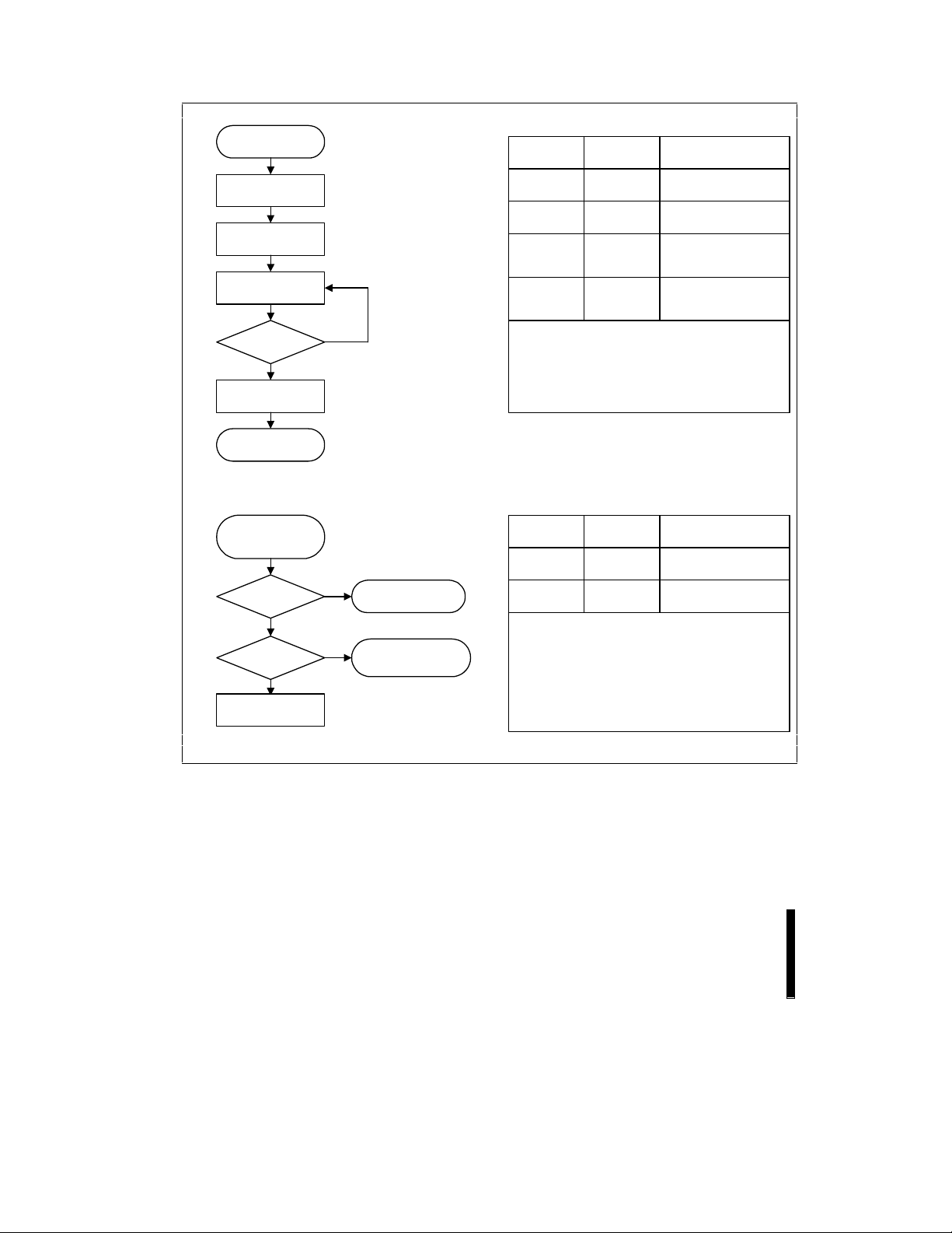
command. Figure 7 shows the
Programming Flowchart.
was not within
PP
Automated
17
Page 18

28F002BC E
Table 5. Status Register Bit Definition
WSMS ESS ES DWS VPPS R R R
76543210
NOTES:
SR.7 = WRITE STATE MACHINE STATUS (WSMS)
1 = Ready
0 = Busy
SR.6 = ERASE-SUSPEND STATUS (ESS)
1 = Erase Suspended
0 = Erase In Progress/Completed
SR.5 = ERASE STATUS
1 = Error In Block Erasure
0 = Successful Block Erase
SR.4 = PROGRAM STATUS
1 = Error in Byte Program
0 = Successful Byte Program
SR.3 = VPP STATUS
1 = V
Low Detect, Operation Abort
PP
0 = V
OK
PP
SR.2–SR.0 = RESERVED FOR FUTURE
ENHANCEMENTS
The Write State Machine bit must first be checked to
determine program or block erase completion, before
the program or erase status bits are checked for
success.
When erase suspend is issued, the WSM halts
execution and sets both the WSMS and ESS bits to
“1.” The ESS bit remains set to “1” until an Erase
Resume command is issued.
When this bit is set to “1,” the WSM has applied the
maximum number of erase pulses to the block and is
still unable to successfully verify block erasure.
When this bit is set to “1,” the WSM has attempted
but failed to program a byte.
The V
provide continuous indication of V
check the V
interrogates V
status bit, unlike an A/D converter, does not
PP
level intermittently. The WSM
PP
level only after the program or
PP
level, but it does
PP
erase command sequences have been entered, and
informs the system if V
If V
ever goes below V
PP
Suspend)
, the status register will set this bit and
abort the operation in progress, even if V
returned to a valid level. The V
guaranteed to report accurate feedback between
V
PPLK
and V
PPH
.
has not been switched on.
PP
PPLK (even during an Erase
is
PP
status bit is not
PP
These bits are reserved for future use and should be
masked out when polling the status register.
3.3.4 ERASE MODE
Erase Setup and Erase Confirm c ommands to the
CUI, along with the address identifying the block to
be erased. This address is l atched internally when
the Erase Confirm command is issued. Block
erasure results in all bits within the bloc k being set
to “1.”
If the Erase Confirm command does not follow the
Erase Setup command, the status register
responds by setting both SR.4 and SR.5 to “1” t o
indicate an invalid command sequence. The WSM
returns to read status register mode.
18
The WSM then executes a sequence of internally
timed events to:
1. Program all bits within the block to “0.”
2. Verify that all bits within the block are
sufficiently programmed to “0.”
3. Erase all bits within the block (set all bits to “1”).
4. Verify that all bits within the block are
sufficiently erased.
While the erase sequence is executing, bit 7 of the
status register is a “0.”
PRELIMINARY
Page 19

E 28F002BC
When the status register indicates that erasure is
complete, the status bits, which indicate whether
the erase operation was successful, should be
checked. If the eras e operation was unsuccessful ,
bit 5 of the status register will be set (within 1.5 ms)
to “1,” indicating an erase failure. If V
acceptable during the suspended period, the WSM
does not execute the erase sequence; ins tead, bit 5
of the status register is s et to a “1” to indicate an
erase failure, and bit 3 is s et t o a “1” t o i ndicat e that
the V
supply voltage was outside acceptable
PP
limits.
The status register should be cleared before
attempting the next operat ion. Any CUI instruction
can follow after erasure is completed; however,
reads from the memory array cannot be
accomplished until the CUI is giv en the Read Array
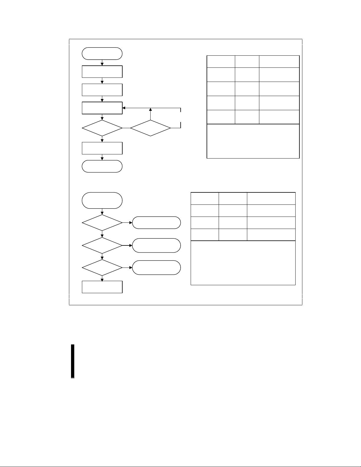
command. Figure 8 details the
Erase Flowchart.
3.3.4.1 Suspending and Resuming Erase
Since an erase operation may tak e a few seconds
to complete, an Erase Suspend command is
provided. This allows erase-sequence interruption
in order to read data from another block of the
memory array. Once the erase s equence is s tarted,
writing the Erase Suspend command to the CUI
requests that the WSM paus e the erase sequence
at a predetermined point in the erase al gori thm. The
status register must then be read to determ ine if the
erase operation has been suspended. Taking V
below V
the operation in progress. V
tained at valid levels, even during Erase Suspend.
At this point, a Read Array com mand c an be wri tt en
to the CUI in order to read data from blocks other
than that being erased. The only other valid
commands at this time are Erase Resume and
Read Status Register.
During erase suspend mode, the chi p can go into a
pseudo-standby mode by tak ing CE# to V
reduces active current draw.
To resume the erase operation, the chip must be
enabled by taking CE# to V
Erase Resume command. When the Erase Resume
command is given, the WSM will continue with the
latches the VPP low status and aborts
PPLK
PP
is not within
PP
Automated Block
should be main-
, which
IH
, then issuing the
IL
PP
erase sequence and finish erasing the block. As
with the end of a standard erase operation, the
status register must be read, cleared, and the next
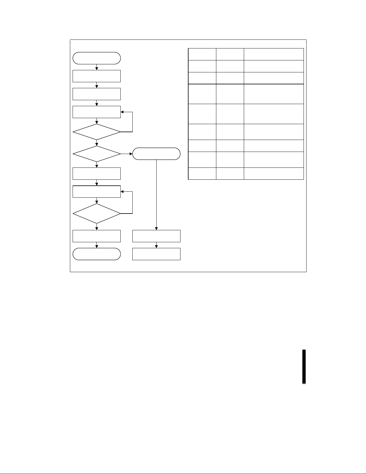
instruction issued in order to continue. Figure 9
highlights the
3.3.5 EXTENDED CYCLING
Intel has designed extended cy cling capability into
its ETOX IV flash memory technology. The
28F002BC flash memory is designed for 100,000
program/erase cycles on each of the five blocks. At
10% V
10,000 program/erase cycles. The combination of
low electric fields, clean oxide processing and
minimized oxide area per memory cell s ubjected to
the tunneling electric field results in very high
cycling capability.
Erase Suspend/Resume Flowchart
, the parameter blocks are capable of
PP
.
3.4 Boot Block Locking
The Boot Block memory architecture features a
hardware-lockable boot block so that the kernel
code for the system can be kept secure while the
parameter and main blocks are programmed and
erased independently as necessary. Onl y the boot
block can be locked independently from the other
blocks.
3.4.1 V
For complete write protection of all blocks in the
flash device, the V
held low. When V
erase operation will cause the device to set an error
bit in the status register.
3.4.2 RP# = V
In the case of boot block modifications (write and
erase), RP# and V
However, if RP# is not at V
erase operation of the boot block is attempted, the
corresponding status regist er bit (Bit 4 for Program
and Bit 5 for Erase, refer to Table 5 for status
register definitions) is s et to indicate the failure to
complete the specified operation.
= VIL FOR COMPLETE
PP
PROTECTION
programming voltage can be
PP
is below V
PP
FOR BOOT BLOCK
HH
UNLOCKING
are set to VHH (12 V).
PP
HH
, any program or
PPLK
when a program or
PRELIMINARY
19
Page 20
28F002BC E
Start
Write 40H and
Byte Address
Write Data and
Data Address
Read
Status Register
SR.7 = 1 ?
No
Yes
Full Status
Check if Desired
Program Complete
FULL STATUS CHECK PROCEDURE
Read Status
Register Data
(See Above)
1
SR.3 =
VPP Range Error
0
1
SR.4 =
Program Error
0
Program
Successful
Bus
Operation
Write
Write
Read
Standby
Repeat for subsequent writes.
SR Full Status Check can be done after each write, or after a
sequence of writes.
Write FFH after the last write operation to reset device to read
array mode.
Bus
Operation
Standby
Standby
SR.3
must
further attempts are allowed by the Write State Machine.
SR.4 is only cleared by the Clear Status Register command, in
cases where multiple bytes are programmed, before full status
is checked.
If an error is detected, clear the status register before
attempting retry or other error recovery.
Command
Program Setup
Program
Command Comments
be cleared, if set during a program attempt, before
Comments
Data = 40H
Addr = Byte to Program
Data = Data to Program
Addr = Location to Program
Status Register Data
Toggle CE# or OE# to
Update SRD
Check SR.7
1 = WSM Ready
0 = WSM Busy
Check SR.3
1 = V
Low Detect
PP
Check SR.4
1 = Program Error
0578_07
20
Figure 7. Automated Programming Flowchart
PRELIMINARY
Page 21
E 28F002BC
Start
Write 20H and
Block Address
Write D0H and
Block Address
Read
Status Register
SR.7 =
0
Suspend Erase
Yes
Full Status
Check if Desired
Program Complete
FULL STATUS CHECK PROCEDURE
Read Status
Register Data
(See Above)
1
SR.3 =
VPP Range Error
0
1
SR.4, 5 =
Command Sequence
Error
0
1
Block Erase ErrorSR.5 =
0
Block Erase
Successful
Suspend Erase Loop
Yes
Operation
SR.3
further attempts are allowed by the Write State Machine.
SR.5 is only cleared by the Clear Status Register command, in
cases where multiple blocks areeased, before full status is
checked.
If an error is detected, clear the status register before
attempting retry or other error recovery.
Bus
Operation
Write
Write
Read
Standby
Repeat for subsequent block erasures.
Full Status Check can be done after each block erase,
or after a sequence of block erasures.
Write FFH after the last operation to reset device to
read array mode.
Bus
Standby
Standby
Standby
must
be cleared, if set during an erase attempt, before
Command
Erase Setup
Erase
Confirm
Command Comments
Check SR.3
1 = V
Check SR.4, 5
Both 1 = Command
Sequence Error
Check SR.5
1 = Block Erase Error
Comments
Data = 20H
Addr = Within Block to
be Erased
Data = D0H
Addr = Within Block to
be Erased
Status Register Data
Toggle CE# or OE# to
Update SRD
Check SR.7
1 = WSM Ready
0 = WSM Busy
Low Detect
PP
0578_08
PRELIMINARY
Figure 8. Automated Block Erase Flowchart
21
Page 22
28F002BC E
Start
Write B0H
Write 70H
Read Status Register
SR.7 =
1
SR.6 =
1
Write FFH
Read Array Data
Done
Reading
Yes
No
0
0
Erase Resumed
Bus
Operation
Write
Write
Write
Read
Standby
Standby
Write
Read
Write
Command
Command
Program
Program
Erase
Suspend
Suspend
Suspend
Read Status
Read Array
Erase
Resume
Comments
Data = B0H
Addr = X
Data =70H
Addr =X
Status Register Data
Toggle CE# or OE# to Update
Status Register Data
Addr = X
Check SR.7
1 = WSM Ready
0 = WSM Busy
Check SR.6
1 = Erase Suspended
0 = Erase Completed
Data = FFH
Addr = X
Read array data from block
other than the one being
programmed
Data = D0H
Addr = X
Write FFHWrite D0H
Erase Resumed Read Array Data
Figure 9. Erase Suspend/Resume Flowchart
22
0578_09
PRELIMINARY
Page 23

E 28F002BC
3.5 Power Consumption
3.5.1 ACTIVE POWER
With CE# at a logic-low lev el and RP# at a logichigh level, the device is placed in the active mode.
The device I
10 MHz with TTL input signals.
3.5.2 STANDBY POWER
With CE# at a logic-high level (V
placed in standby mode, where the maximum I
standby current is 100 µA. The s tandby operation
disables much of the device’s circuitry and
substantially reduces device power consumption.
The outputs (DQ[0:7]) are placed in a highimpedance state independent of the status of the
OE# signal. When CE# is at a logic-high level
during erase or program, the device will continue to
perform the erase or program function and
consume erase or program activ e power unt il eras e
or program is completed.
3.5.3 DEEP POWER-DOWN
The 28F002BC flash memory supports a ty pical I
of 0.2 µA in deep power-down mode. This mode is
activated by the RP# pin when it is at a logic -low
(GND ± 0.2 V); in this mode, all internal circui ts are
turned off to save power.
Setting the RP# pin low de-sel ects t he mem ory and
places the output drivers in a high impedanc e st ate.
Recovery from the deep power-down state requires
a minimum access t ime of 300 ns (Sect ion 4.5,
Characteristics—Read-Only Operations
parameter).
During erase or program modes, RP# low will abort
either erase or program operations, but the mem ory
contents are no longer valid as t he data has been
corrupted. RP# transitions to V
off to the device will clear the status register.
current is a maximum of 60 mA at
CC
), the memory is
IH
, t
or turning power
IL
CC
CC
AC
PHQV
3.6 Power-Up/Down Operation
The 28F002BC offers protection against accidental
block erasure or programming during power
transitions. Power supply sequencing is not
required, since the device is indif ferent as to whic h
power supply, V
is reset to the read mode after power-up, but the
system must drop CE# low or present a new
address to ensure valid data at the outputs.
A system designer must guard against spurious
writes when V
= VHH. Since both WE# and CE# must be low for a
command write, driving either signal to V
inhibit writes to the device. The CUI architecture
provides additional protection since alteration of
memory contents can only occur after successful
completion of the two-step command sequences.
The device is also disabl ed until RP# is brought to
V
, regardless of the stat e of its c ontrol inputs. By
IH
holding the device in reset (RP# connected to
system PowerGood/Reset) during power-up/down,
invalid bus conditions during power-up can be
masked, providing yet another level of memory
protection.
3.6.1 RP# CONNECTED TO SYSTEM
The use of RP# during system reset is important
with automated write/erase devices because the
system expects to read from the flash memory
when it comes out of reset . If a CPU reset occurs
without a flash memory reset, proper CPU
initialization would not occur because the flash
memory may be providing status information
instead of array data. Intel ’s Flash memories allow
proper CPU initialization following a system reset
by connecting the RP# pin to the same RESET#
signal that resets the system CPU.
3.6.2 V
The CUI latches commands as issued by system
software and is not altered by V
or WSM actions. Its default state upon power-up,
after exit from deep power-down m ode, or after V
transitions above V
After any program or block erase operation is
complete, and even after V
V
, the CUI must be reset to read array mode
PPLK
via the Read Array command if access to the fl ash
memory is desired.
or VCC, powers-up first. The CUI
PP
voltages are above V
CC
RESET
, VPP AND RP# TRANSITIONS
CC
, CE# transitions ,
PP
, is read array mode.
LKO
transitions down to
PP
LKO
and V
IH
will
CC
PP
PRELIMINARY
23
Page 24

28F002BC E
3.7 Power Supply Decoupling
Flash memory’s power switching characteristics
require careful device decoupli ng methods. System
designers should consider three supply current
issues:
1. Standby current levels (I
2. Active current levels (I
3. Trans ient peaks produced by falling and rising
edges of CE#
Transient current magnitudes depend on t he devi ce
outputs’ capacitiv e and inductive loading. Two-line
control and proper decoupling capacitor selection
will suppress these transient voltage peaks. Each
flash device should have a 0.1 µF ceramic
capacitor connected between eac h V
and between its V
PP
frequency, inherently low-inductance capacitors
should be placed as close as possible to the
package leads.
)
CCS
)
CCR
and GND,
CC
and GND. These high-
3.7.1 V
TRACE ON PRINTED CIRCUIT
PP
BOARDS
Designing for in-system writes to the flash memory
requires special consideration of the V
supply trace by the printed circuit board designer.
The V
pin supplies the flash m emory c ells current
PP
PP
power
for programming and erasing. One should use
similar trace widths and layout consi derations given
to the V
power supply trace. Adequate V
CC
supply traces and decoupling capacitors placed
adjacent to the component will decrease spik es and
overshoots.
PP
24
PRELIMINARY
Page 25
E 28F002BC
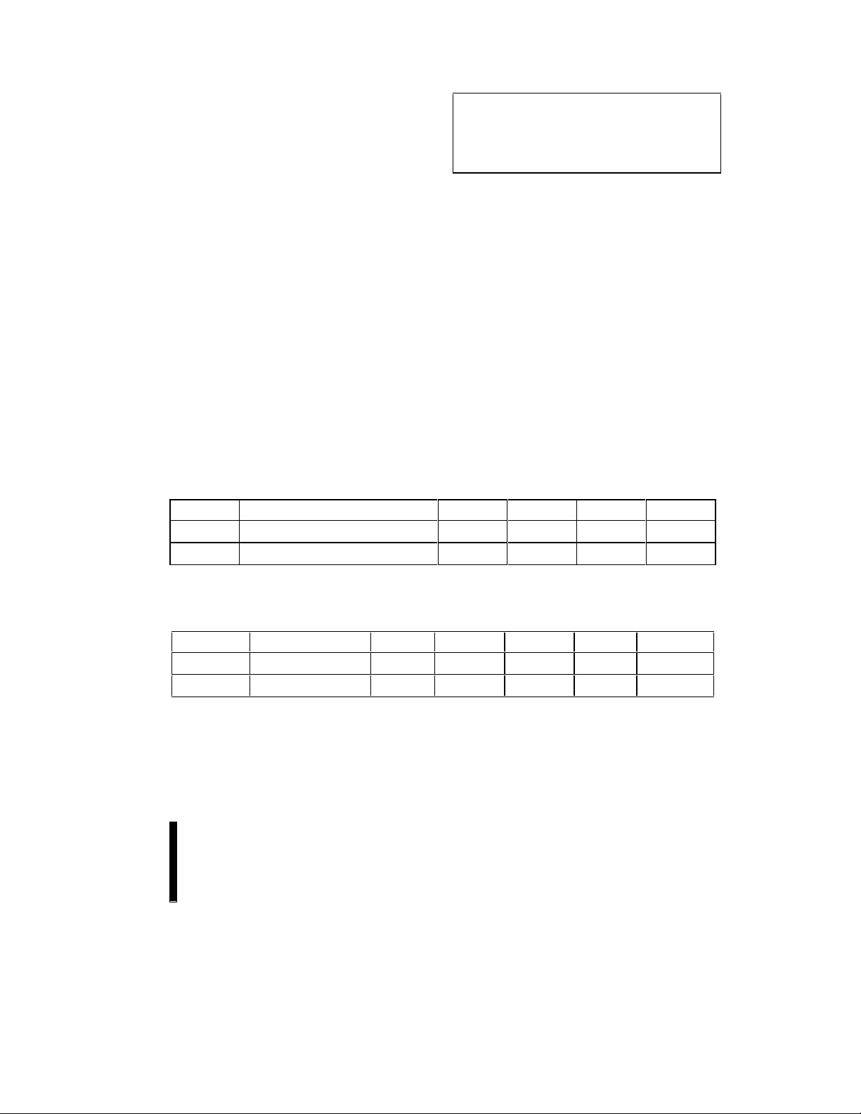
4.0 ELECTRICAL SPECIFICATIONS
4.1 Absolute Maximum Ratings*
Operating Temperature
During Read...............................0 °C to +70 °C
During Write and Block Erase ....0 °C to +70 °C
Temperature Bias...................–10 °C to +80 °C
Storage Temperature.................–65 °C to +125 °C
Voltage on Any Pin (except V
with Respect to GND............–2.0 V to +7.0 V
Voltage on Pin RP# or Pin A
with Respect to GND.......–2.0 V to +13.5 V
VPP Program Voltage
with Respect to GND during Write
and Block Erase.............–2.0 V to +14.0 V
VCC Supply Voltage
with Respect to GND...........–2.0 V to +7.0 V
Output Short Circuit Current.................... 100 mA
, VPP, A9 and RP#)
CC
9
(1, 2)
(1, 2)
NOTICE: This datasheet contains preliminary information on
new products in production. Do not finalize a desi gn with
this information. Revised information will be published when
the product is available. Verify with your local Intel Sales
office that you have the latest datasheet before finalizing a
design.
* WARNING: Stressing the device beyond the "Absolute
Maximum Ratings" may cause permanent damage. These
are stress ratings only. Operation beyond the "Operating
Conditions" is not recommended and extended exposure
beyond the "Operating Conditions" may effect device
reliability.
NOTES:
(1)
1. Minimum DC voltage is -0.5 V on input/output pins.
During transitions, this level may undershoot to -2.0 V
for periods <20 ns. Maximum DC voltage on
input/output pins is V
transitions, may overshoot to V
<20 ns.
2. Maximum DC voltage on V
for periods <20 ns. Maximum DC voltage on RP# or A
may overshoot to 13.5 V for periods <20 ns.
3. Output shorted for no more than one second. No more
(1)
(3)
than one output shorted at a time.
+ 0.5 V which, during
CC
+ 2.0 V for periods
CC
may overshoot to +14.0 V
PP
4.2 Operating Conditions
Table 6. Temperature and VCC Operating Conditions
Symbol Parameter Notes Min Max Units
T
A
V
CC
Operating Temperature 0 70 °C
5 V VCC Supply Voltage (10%) 4.50 5.50 Volts
9
4.3 Capacitance
TA = +25° C, f = 1 MHz
Symbol Parameter Notes Typ Max Unit Conditions
C
IN
C
OUT
NOTES:
1. Sampled, not 100% tested.
2. For the 28F002BC, address pin A
Input Capacitance 1 6 8 pF VIN = 0 V
Output Capacitance 1, 2 10 12 pF V
follows the C
10
capacitance numbers.
OUT
PRELIMINARY
OUT
= 0 V
25
Page 26
28F002BC E
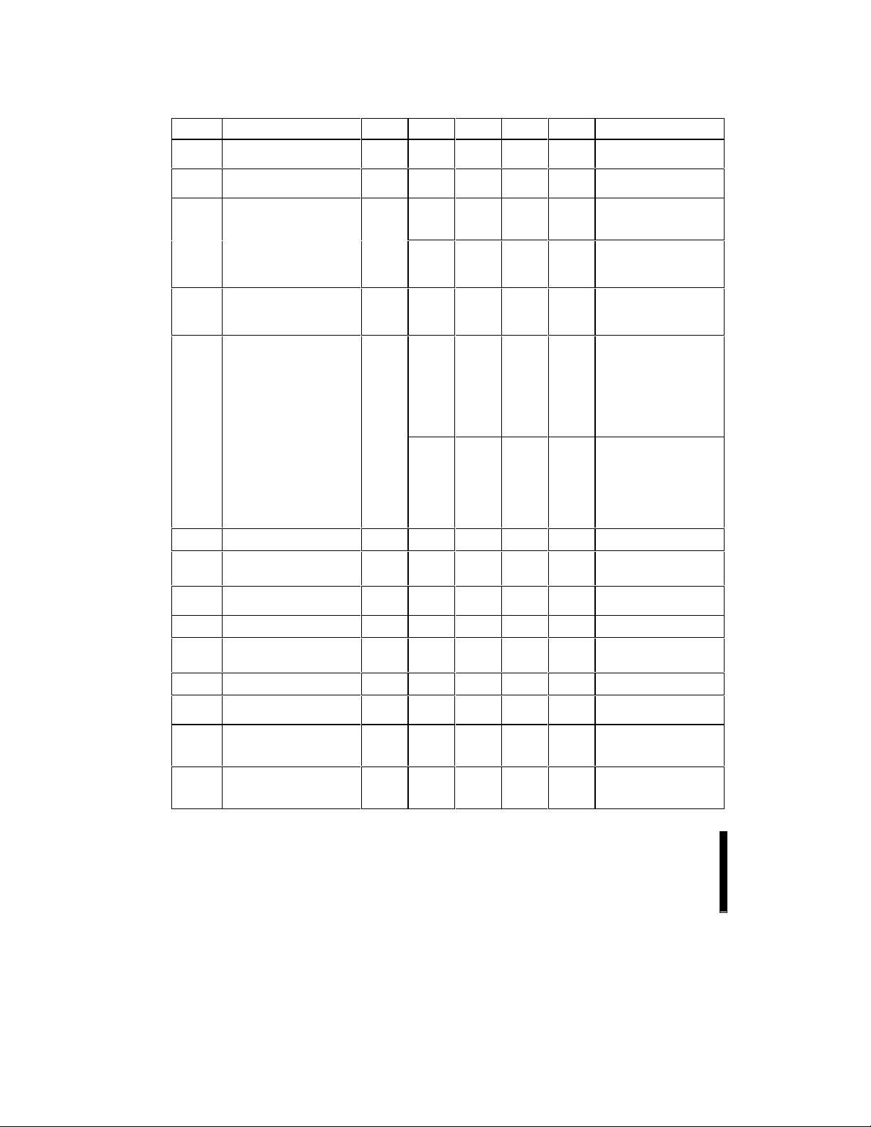
4.4 DC Characteristics
Symbol Parameter Notes Min Typ Max Units Test Conditions
= V
I
IL
I
LO
I
CCS
I
CCD
I
CCR
I
CCW
I
CCE
I
CCES
I
PPS
I
PPD
I
PPR
I
PPW
I
PPE
I
PPES
V
Input Load Current 1 ± 1.0 µA
Output Leakage Current 1 ± 10 µA
VCC Standby Current 1,3 1.5 mA
50 100 µA
CC
V
IN
V
CC
V
IN
V
CC
CE# = RP# = WP# =
V
CC
CE# = RP# = V
VCC Deep Power-Down
Current
1 0.2 8.0 µA
VCC = V
V
IN
RP# = GND ± 0.2 V
VCC Read Current
1,5 20 55 mA
V
CC
CE# = GND
f = 10 MHz
I
OUT
CMOS Inputs: GND ±
20 60 mA
V
CC
CE# = V
f = 10 MHz
I
OUT
TTL Inputs: V
VCC Program Current 1,4 50 mA Byte Prog. in Progress
VCC Erase Current 1,4 30 mA Block Erase in
VCC Erase Suspend
Current
1,2 5 10 mA
VPP Standby Current 1 ± 10 µA V
VPP Deep Power-Down
1 5.0 µA RP# = GND ± 0.2 V
CE# = V
Block Erase Suspend
PP
Current
V
Read Current 1 200 µA VPP > V
PP
V
VPP Program Current 1,4 20 mA
VPP Erase Current 1,4 15 mA
VPP Erase Suspend
Current
1 200 µA
PP
Byte Prog. in Progress
V
PP
Block Erase in
VPP = V
Block Erase
Max
CC
= VCC or GND
= V
Max
CC
= VCC or GND
= V
Max
CC
V
IH
= V
Max
CC
CC
0.2 V
Max
CC
= VCC or GND
CMOS INPUTS
= V
Max
CC
= 0 mA
0.2 V or V
± 0.2 V
CC
TTL INPUTS
= V
Max
CC
IL
= 0 mA
or V
IL
Progress
IH
≤ V
CC
CC
= V
PPH
= V
PPH
Progress
PPH
Suspended
±
IH
26
PRELIMINARY
Page 27

E 28F002BC
4.4 DC Characteristics (Continued)
Symbol Parameter Notes Min Typ Max Units Test Conditions
I
RP#
I
ID
V
V
V
V
V
V
V
V
V
V
NOTES:
1. All currents are in RMS unless otherwise noted. Typical values at V
2. I
3. Block erases and byte writes are inhibited when V
4. Sampled, not 100% tested.
5. CMOS Inputs are either V
6. V
7. V
8. V
RP# Boot Block Unlock
1,4 500 µA RP# = V
HH
Current
A9 Intelligent Identifier
Current
A9 Intelligent Identifier
ID
Voltage
Input Low Voltage -0.5 0.8 V
IL
Input High Voltage 2.0
IH
Output Low Voltage 0.45 V
OL
Output High Voltage
OH
(TTL)
Output High Voltage
(CMOS)
PPLKVPP
PPH
PPH
LKO
HH
are valid for all product versions (packages and speeds).
CCES
of I
CC
PP
PP
cycles; main blocks support up to 100 block erase cycles. Note that erase times are close to maximum spec limits when
using this option.
Lock-Out Voltage 3 0.0 6.5 V
VPP (Program/
Erase Operations)
VPP (Program/
Erase Operations)
VCC Erase/Write Lock
Voltage
RP# Unlock Voltage 8 10.8 12.0 13.2 V Boot Block Unlock
is specified with the device de-selected. If the device is read while in erase suspend mode, current draw is the sum
and I
CCES
= 5.0 V ± 10% for applications requiring 100,000 block erase cycles.
= 12.0 V ± 5% for applications requiring 100,000 block erase cycles.
= 12.0 V ± 10% for applications requiring wider VPP tolerances: Parameter blocks can sustain 10,000 block erase
CCR
.
± 0.2 V or GND ± 0.2 V. TTL Inputs are either VIL or VIH.
CC
1,4 500 µA A
10.8 13.2 V
+
V
CC
0.5V
V
2.4 V
0.85
V
V
CC
CC
–
V
0.4V
7 11.4 12.0 12.6 V
8 10.8 12.0 13.2 V
2.0 V
= 5.0 V, VPP =12.0 V , T = +25 °C. These currents
CC
= V
PP
, and not guaranteed in the range between V
PPLK
= V
9
ID
= V
V
CC
I
OL
V
CC
I
OH
V
CC
I
OH
V
CC
I
OH
Min
CC
= 5.8 mA
= V
Min
CC
= –2.5 mA
= V
Min
CC
= –1.5 mA
= V
Min
CC
= –100 µA
Complete Write
Protection
Voltage
and V
PPH
PPLK
.
PRELIMINARY
27
Page 28
28F002BC E
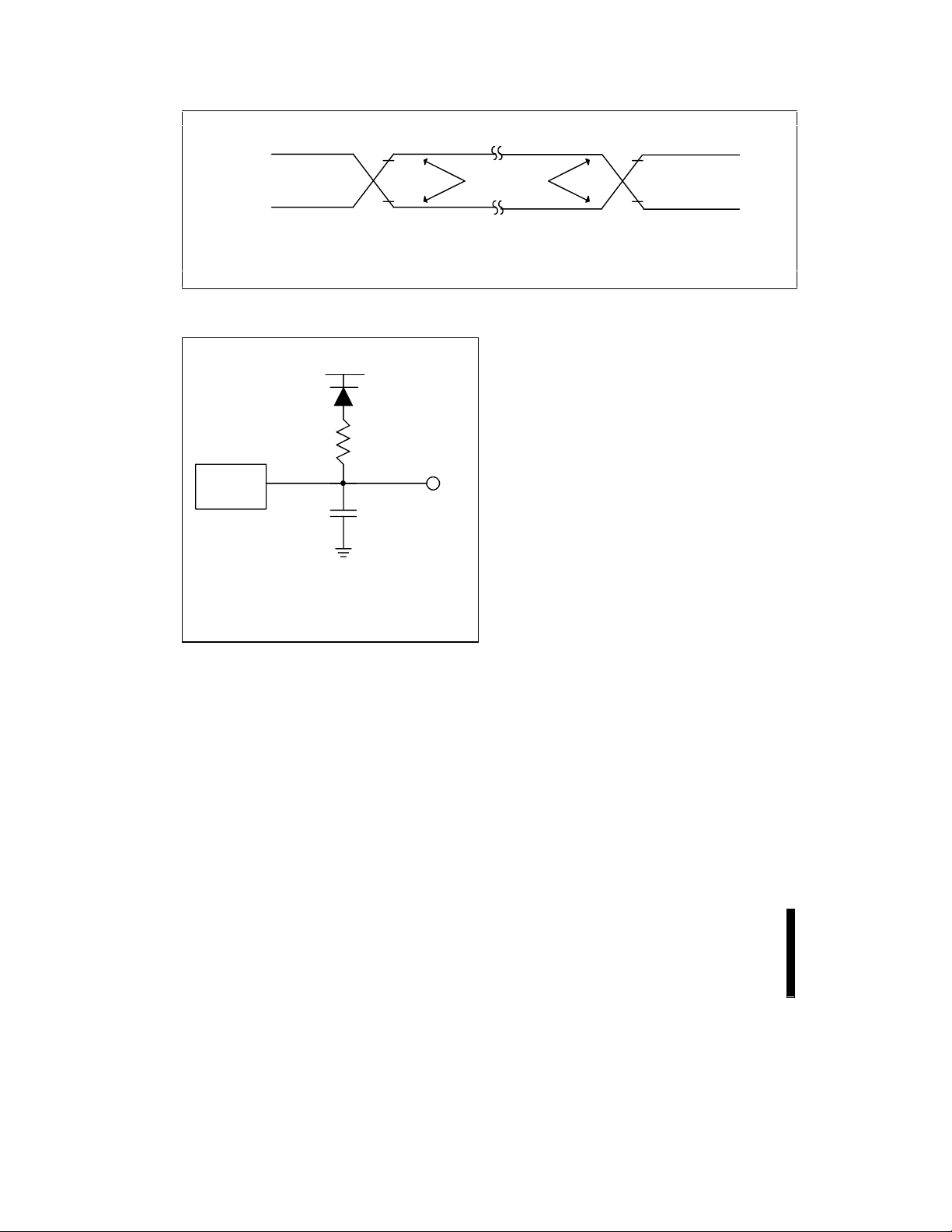
2.4
INPUT OUTPUT
0.45
NOTE:
AC test inputs are driven at VOH (2.4 V
and VIL (0.8 V
DEVICE
UNDER
TEST
). Output timing ends at VIH and VIL.
TTL
1.3V
1N914
NOTES:
CL = 100 pF, includes Jig Capacitance
RL = 3.3KΩ
2.0
TEST POINTS
0.8
) for a logic “1” and VOL (0.45 V
TTL
) for a logic “0.” Input timing begins at VIH (2.0 V
TTL
Figure 10. Inputs and Measurement Points
R
L
OUT
C
L
0578_11
2.0
0.8
0578_10
TTL
)
Figure 11. Standard Test Configuration
28
PRELIMINARY
Page 29
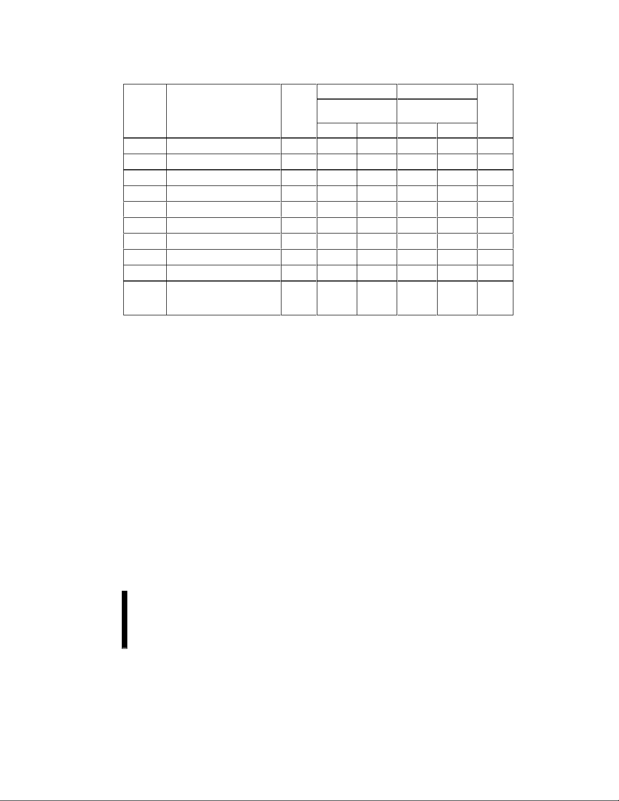
E 28F002BC
4.5 AC Characteristics—Read-Only Operations
28F002BC-80 28F002BC-120
Symbol Parameter Notes V
t
AVAV
t
AVQV
t
ELQV
t
PHQV
t
GLQV
t
ELQX
t
EHQZ
t
GLQX
t
GHQZ
t
OH
NOTES:
1. See
2. OE# may be delayed up to t
3. Sampled, but not 100% tested.
4. See
Read Cycle Time 80 120 ns
Address to Output Delay 80 120 ns
CE# to Output Delay 2 80 120 ns
RP# to Output Delay 300 300 ns
OE# to Output Delay 2 40 40 ns
CE# to Output in Low Z 3 0 0 ns
CE# to Output in High Z 3 30 30 ns
OE# to Output in Low Z 3 0 0 ns
OE# to Output in High Z 3 30 30 ns
Output Hold from Address,
CE#, or OE# Change,
Whichever Occurs First
Inputs and Measurement Points
CE—tOE
Standard Test Configuration
(Figure 11).
(Figure 10).
after the falling edge of CE# without impact on tCE.
30 0 ns
= 5 V ± 10%
CC
100 pF
Min Max Min Max
(1)
V
= 5 V ± 10%
CC
100 pF
Units
PRELIMINARY
29
Page 30
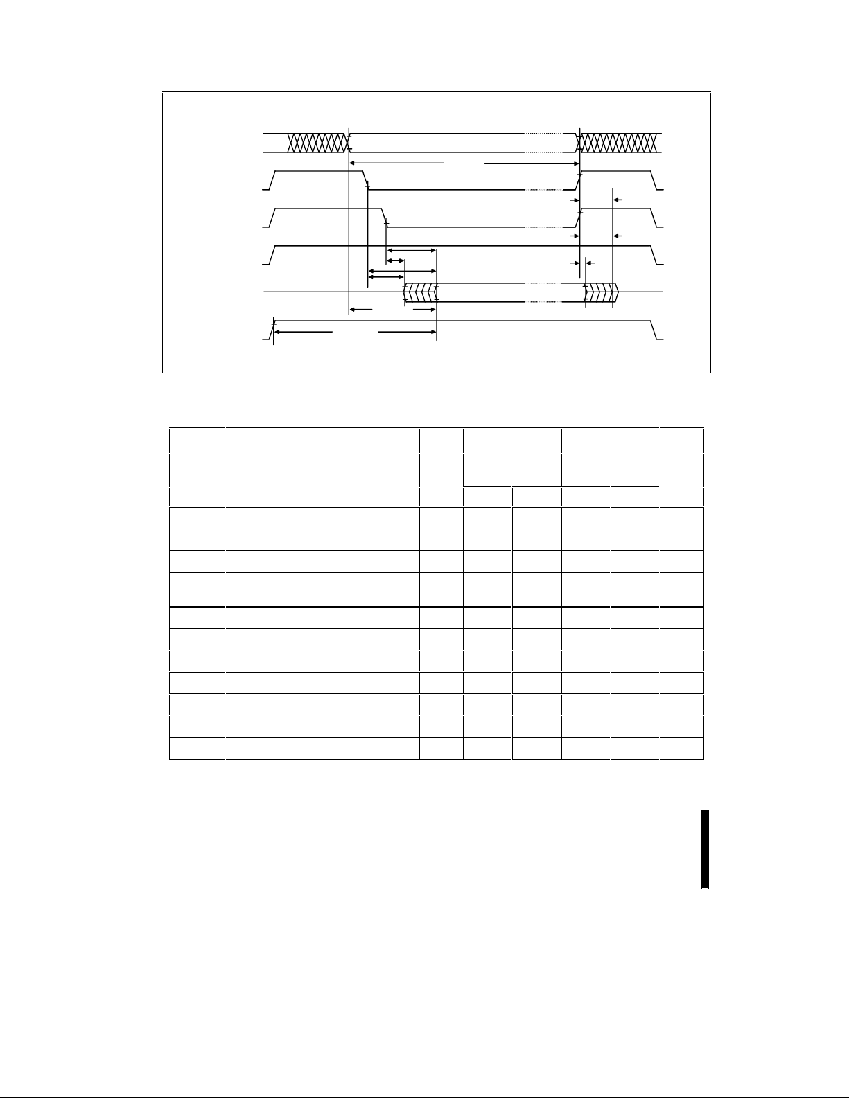
28F002BC E
Data
Valid Standby
t
AVAV
Valid Output
t
V
ADDRESSES (A)
CE# (E)
OE# (G)
WE# (W)
DATA (D/Q)
RP#(P)
IH
V
IL
V
IH
V
IL
V
IH
V
IL
V
IH
V
IL
V
OH
V
OL
V
IH
V
IL
High Z
Device and
Address Selection
Address Stable
t
ELQX
t
AVQV
t
PHQV
t
GLQX
t
GLQV
t
ELQV
Figure 12. AC Waveforms for Read Operations
4.6 AC Characteristics—WE#-Controlled Write Operations
28F002BC-80 28F002BC-120
Symbol Parameter Notes V
t
AVAV
t
PHWL
t
ELWL
t
PHHWH
t
VPWH
t
AVWH
t
DVWH
t
WLWH
t
WHDX
t
WHAX
t
WHEH
Write Cycle Time 80 120 ns
RP# Setup to WE# Going Low 215 215 ns
CE# Setup to WE# Going Low 0 0 ns
Boot Block Lock Setup to WE#
6, 8 100 100 ns
Going High
VPP Setup to WE# Going High 5, 8 100 100 ns
Address Setup to WE# Going High 3 50 50 ns
Data Setup to WE# Going High 4 50 50 ns
WE# Pulse Width 50 50 ns
Data Hold Time from WE# High 4 0 0 ns
Address Hold Time from WE# High 3 0 0 ns
CE# Hold Time from WE# High 0 0 ns
= 5 V ± 10%
CC
100 pF
Min Max Min Max
OH
(1)
V
CC
t
EHQZ
t
GHQZ
High Z
= 5 V ± 10%
100 pF
0578_12
Units
30
PRELIMINARY
Page 31
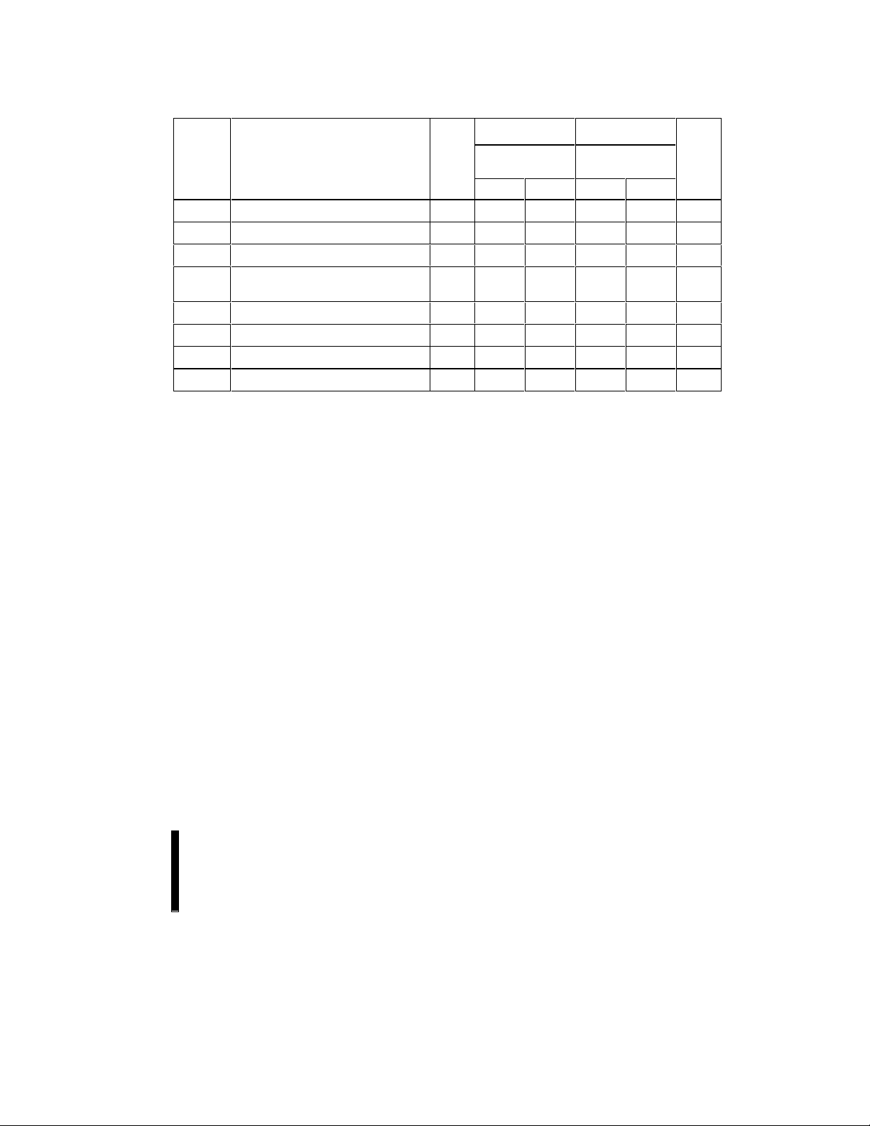
E 28F002BC
4.6 AC Characteristics—WE#-Controlled Write Operations
28F002BC-80 28F002BC-120
Symbol Parameter Notes V
t
WHWL
t
WHQV1
t
WHQV2
t
WHQV3
t
WHQV4
t
QVVL
t
QVPH
t
PHBR
NOTES:
1. Read timing characteristics during write and erase operations are the same as during read-only operations. Refer to
Characteristics—Read-Only Operations
2. The on-chip WSM completely automates program/erase operations; program/erase algorithms are now controlled internally
which includes verify and margining operations.
3. Refer to command definition table for valid A
4. Refer to command definition table for valid D
5. Program/erase durations are measured to valid SRD data (successful operation, SR.7 = 1).
6. For boot block program/erase, RP# should be held at V
7. Time t
8. Sampled, but not 100% tested.
WE# Pulse Width High 20 20 ns
Duration of Programming Operation 2, 5 6 6 µs
Duration of Erase Operation (Boot) 2, 5, 6 0.3 0.3 s
Duration of Erase Operation
(Parameter)
Duration of Erase Operation (Main) 2, 5 0.6 0.6 s
V
Hold from Valid SRD 5, 8 0 0 ns
PP
RP# VHH Hold from Valid SRD
Boot Block Lock Delay 7, 8 100 100 ns
during read mode.
.
IN
.
IN
is required for successful relocking of the boot block.
PHBR
2,5 0.3 0.3 s
6, 8 0 0 ns
until operation completes successfully.
HH
= 5 V ± 10%
CC
100 pF
Min Max Min Max
(1)
(Continued)
V
= 5 V ± 10%
CC
100 pF
Units
AC
PRELIMINARY
31
Page 32
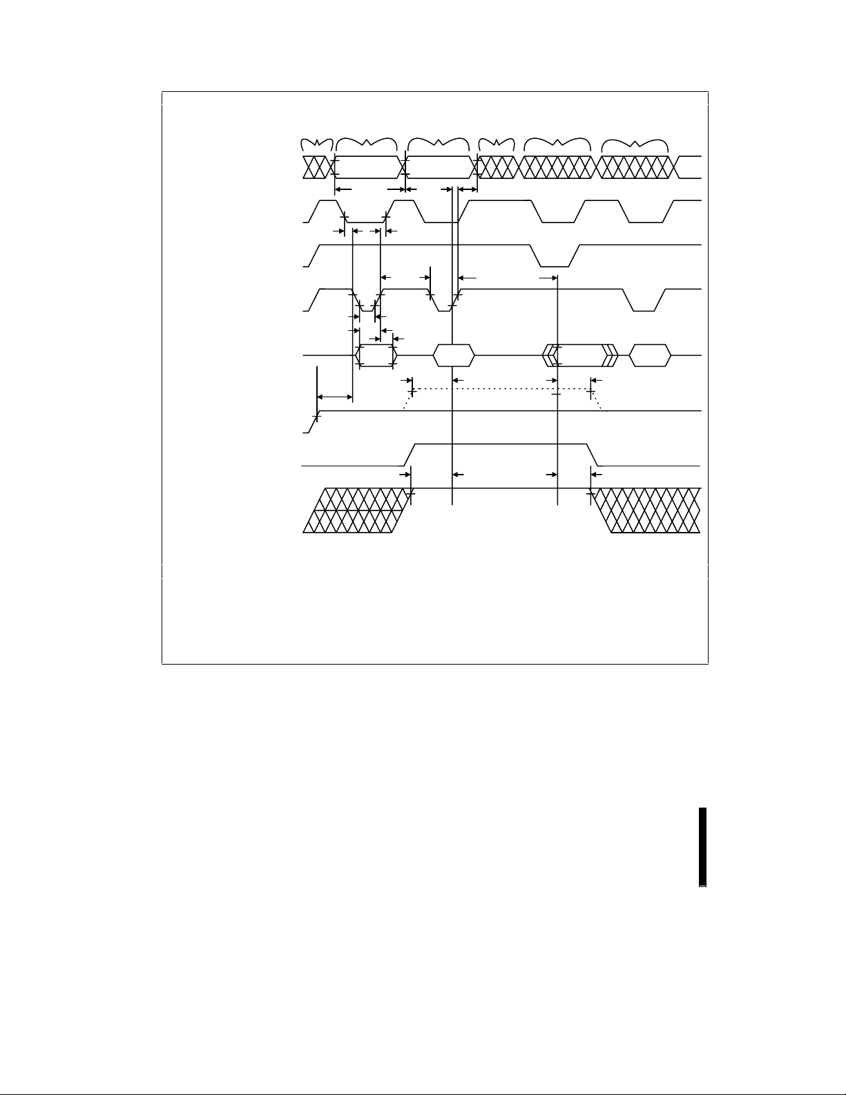
28F002BC E
AB C D E F
V
ADDRESSES (A)
CE# (E)
OE# (G)
WE# (W)
DATA (D/Q)
6.5V
RP# (P)
WP# ()
VPP (V)
IH
V
IL
V
IH
V
IL
t
ELWL
V
IH
V
IL
V
IH
V
IL
V
IH
V
IL
V
HH
V
IH
V
IL
V
IH
V
IL
V
2
PPH
V
1
PPH
V
PPLK
V
IL
NOTES:
A. VCC Power-Up and Standby
B. Write Program Setup or Erase Setup Command
C. Write Valid Address and Data (Program or Erase Confirm Command
D. Automated Program or Erase Delay
E. Read Status Register Data
F. Write Read Array Command
High Z
A
t
AVAV
t
PHWL
t
WHEH
t
WHWL
t
DVWH
t
WHDX
t
AVWH
A
IN
t
WHAX
t
WHQV1,2,3,4
D
IN
t
PHHWH
t
VPWH
Valid
SRD
t
QVPH
t
QVVL
D
IN
0578_13
IN
t
WLWH
D
IN
32
Figure 13. AC Waveforms for Write and Erase Operations (WE#—Controlled Writes)
PRELIMINARY
Page 33
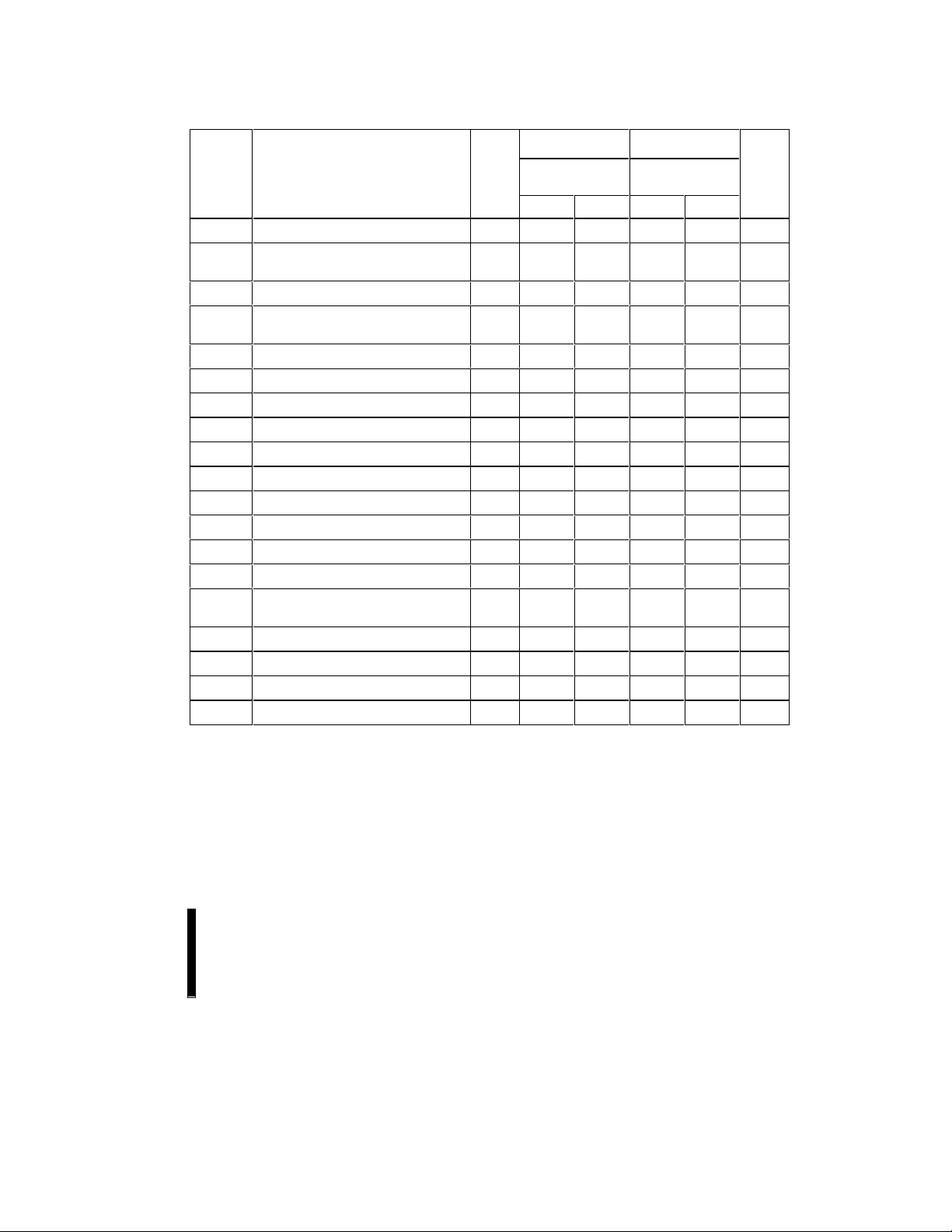
E 28F002BC
4.7 AC Characteristics—CE#-Controlled Write Operations
28F002BC-80 28F002BC-120
Symbol Parameter Notes V
t
AVAV
t
PHEL
t
WLEL
t
PHHEH
t
VPEH
t
AVEH
t
DVEH
t
ELEH
t
EHDX
t
EHAX
t
EHWH
t
EHEL
t
EHQV1
t
EHQV2
t
EHQV3
t
EHQV4
t
QVVL
t
QVPH
t
PHBR
NOTES:
AC Characteristics—WE#-Controlled Write Operations
See
9. Chip-Enable controlled writes: write operations are driven by the valid combination of CE# and WE# in systems where
CE# defines the write pulse-width (within a longer WE# timing waveform), all set-up, hold and inactive WE# times should
be measured relative to the CE# waveform.
Write Cycle Time 80 120 ns
RP# High Recovery to CE# Going
Low
WE# Setup to CE# Going Low 0 0 ns
Boot Block Lock Setup to CE# Going
High
VPP Setup to CE# Going High 5, 8 100 100 ns
Address Setup to CE# Going High 3 50 50 ns
Data Setup to CE# Going High 4 50 50 ns
CE# Pulse Width 50 50 ns
Data Hold Time from CE# High 4 0 0 ns
Address Hold Time from CE# High 3 0 0 ns
WE # Hold Time from CE# High 0 0 ns
CE# Pulse Width High 30 30 ns
Duration of Programming Operation 2, 5 6 6 µs
Duration of Erase Operation (Boot) 2, 5, 6 0.3 0.3 s
Duration of Erase Operation
(Parameter)
Duration of Erase Operation (Main) 2, 5 0.6 0.6 s
VPP Hold from Valid SRD 5, 8 0 0 ns
RP# V
Boot Block Lock Delay 7, 8 100 100 ns
Hold from Valid SRD 6, 8 0 0 ns
HH
6, 8 100 100 ns
2, 5 0.3 0.3 s
for notes 1 through 8.
= 5 V ± 10%
CC
100 pF
Min Max Min Max
215 215 ns
(1, 9)
VCC= 5 V ± 10%
100 pF
Units
PRELIMINARY
33
Page 34
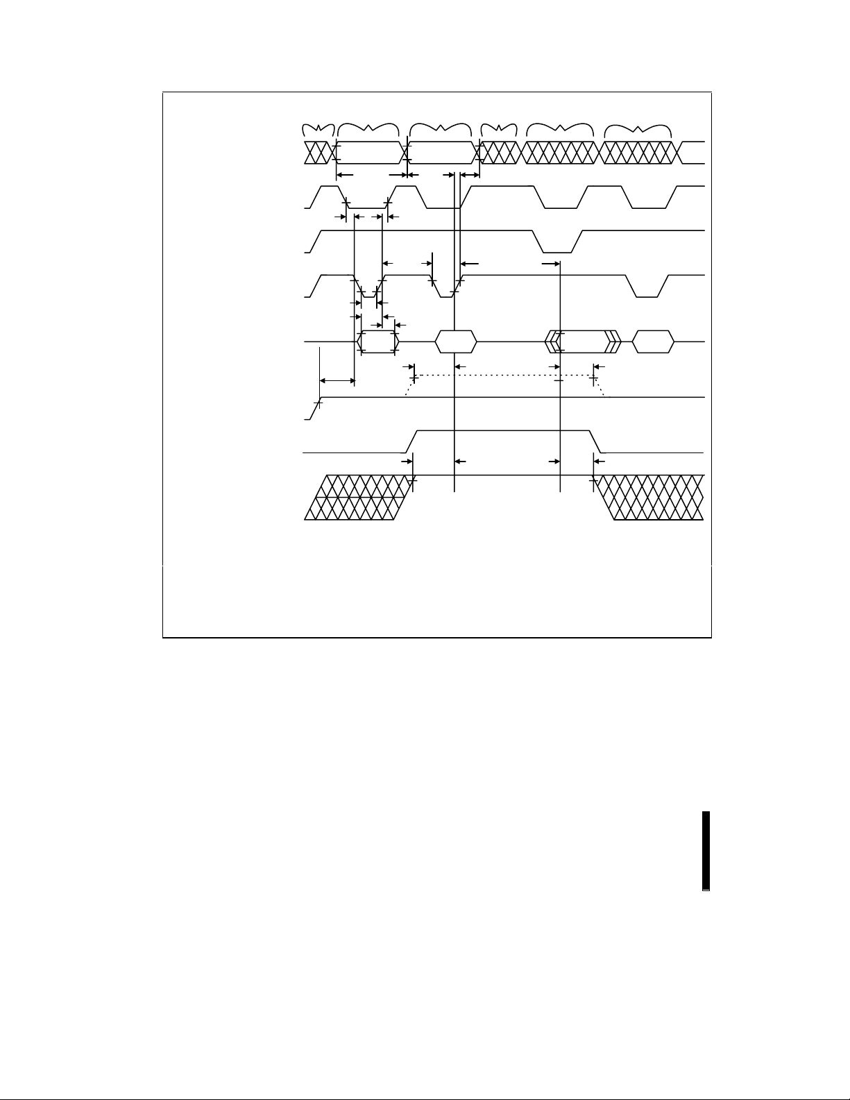
28F002BC E
AB C D E F
V
ADDRESSES (A)
CE# (E)
OE# (G)
WE# (W)
DATA (D/Q)
6.5V
RP# (P)
WP# ()
VPP (V)
IH
V
IL
V
IH
V
IL
t
WLEL
V
IH
V
IL
V
IH
V
IL
V
IH
V
IL
V
HH
V
IH
V
IL
V
IH
V
IL
V
2
PPH
V
1
PPH
V
PPLK
V
IL
NOTES:
A. VCC Power-Up and Standby
B. Write Program Setup or Erase Setup Command
C. Write Valid Address and Data (Program or Erase Confirm Command
D. Automated Program or Erase Delay
E. Read Status Register Data
F. Write Read Array Command
Figure 14. Alternate AC Waveforms for Write and Erase Operations (CE#—Controlled Writes)
High Z
A
t
AVAV
t
PHWL
t
t
ELEH
t
EHWH
EHEL
t
DVEH
t
EHDX
t
AVEH
A
IN
t
EHAX
t
EHQV1,2,3,4
D
IN
t
PHHEH
t
VPEH
Valid
SRD
t
QVPH
t
QVVL
D
IN
0578_14
IN
D
IN
34
PRELIMINARY
Page 35
E 28F002BC
4.8 Erase and Program Timings
TA = +25 °C
= 12 V ± 10%
V
PP
Parameter
Boot/Parameter Block Erase Time 5.8 40 1.0 7 s
Main Block Erase Time 14 60 2.4 14 s
Main Block Write Time 6.0 20 1.2 4.2 s
NOTES:
1. All numbers are sampled, not 100% tested.
2. Erase times near max limits when the 10% V
(1)
V
= 5 V ± 10% V
CC
Typ Max Typ Max
option is used.
PP
(2)
V
= 12 V ± 5%
PP
= 5 V ± 10% Units
CC
5.0 ORDERING INFORMATION
E 2 8 F 0 0 2 B C - T 1 2
Package
E = 40-Lead TSOP
P = 40-Lead PDIP
PA = 44-Lead PSOP
Product line designator
for all Intel® Flash products
0
Access Speed (ns)
(80, 120)
T =
Top Boot
Device/Organization
00X= x8-only (X = 2)
VALID COMBINATIONS:
40-Lead TSOP 40-Lead PDIP 44-Lead PSOP
Commercial 2 M E28F002BC-T80 P28F002BC-T80 PA28F002BC-T80
E28F002BC-T120 P28F002BC-T120 PA28F002BC-T120
PRELIMINARY
Architecture
= Boot Block
B
0578_14
35
Page 36

28F002BC E
6.0 ADDITIONAL INFORMATION
Order Number Document
290580
292161
292163
Note 3
Note 3
Note 3
Note 3
Note 3
Note 3
Note 3
NOTES:
1. Please call the Intel Literature Center at (800) 548-4725 to request Intel documentation. International customers should
contact their local Intel or distribution sales office.
2. Visit Intel’s World Wide Web home page at http://www.intel.com for technical documentation and tools.
3. These documents can be located at the Intel World Wide Web support site, http://www.intel.com/support/flash/memory
3 Volt Advanced Boot Block Flash Memory; 28F004/400B3, 28F008/800B3,
28F016/160B3, 28F320B3
datasheet
AP-608 Implementing a Plug and Play BIOS Using Intel’s Boot Block Flash Memory
AP-610 Flash Memory In-System Code and Data Update Techniques
AB-57 Boot Block Architecture for Safe Firmware Updates
AP-363 Extended Flash BIOS Concepts for Portable Computers
AP-604 Using Intel’s Boot Block Flash Memory Parameter Blocks to Replace EEPROM
28F002/200BX-T/B 2-Mbit Boot Block Flash Memory
28F004/400BX-T/B 4-Mbit Boot Block Flash Memory
28F002/200BV-T/B 2-Mbit SmartVoltage Flash Memory
28F004/400BV-T/B 4-Mbit SmartVoltage Flash Memory
datasheet
datasheet
datasheet
datasheet
36
PRELIMINARY
Page 37
E 28F002BC
APPENDIX A
WSM TRANSITION TABLE
Write State Machine Current/Next States
Command Input (and Next State)
Current
State
Read
Array “1” Array
Program
Setup “1” Status Program (Command Input = Byte Program Data)
Program
(Not
Comp.)
Program
(Comp.) “1” Status
Erase
Setup “1” Status
Erase
Cmd.
Error
Erase
(Not
Comp.)
Erase
(Comp.) “1” Status
Erase
Suspend
to Status
Erase
Suspend
to Array
Read
Status “1” Status
Read
Identifier “1” ID
NOTE:
You cannot program “1”s to the flash. Writing FFH after the Program Setup command will initiate the program algorithm of the
WSM machine. The WSM will attempt the program, realize you are trying to program “1”s, and exit to read status mode without
changing memory contents. No error is returned. Writing another FFH while in read status mode will return the flash to Read
Array.
SR.7 Data
When
Read
*
“0” Status Program
“1” Status
“0” Status
“1” Status
“1” Array
Read
Program
Array
(FFH)
Read
Array
Read
Array
Read
Array
Read
Array
Erase
Susp. to
Array
Erase
Susp. to
Array
Read
Array
Read
Array
Setup
(40H)
Program
Setup
Program
Setup
Erase Command Error
Program
Setup
Program
Setup
Erase
Susp. to
Array
Erase
Susp. to
Array
Program
Setup
Program
Setup
Erase
Setup
(20H)
Erase
Setup Read Array
Erase
Setup
Erase
Setup
Erase
Erase
Setup
Erase
Susp. to
Array
Erase
Susp. to
Array
Erase
Setup
Erase
Setup
Erase
Confirm
(D0H)
Erase
Erase
Erase
Erase
Susp.
(B0H)
Read Array
Erase
Cmd.
Error
Read Array
Erase
Susp. to
Status
Read Array
Erase
Susp. to
Array
Erase
Susp. to
Array
Read Array
Read Array
Erase
Resume
(D0H)
Erase Erase Command Error
Erase
Erase
Read
Status
(70H)
Read
Status
Read
Status
Read
Status
Read
Status
Erase
Susp. to
Status
Erase
Susp. to
Status
Read
Status
Read
Status
Clear
Status
(50H)
Read
Array Read ID
Read
Array Read ID
Read
Array Read ID
Erase
Read
Array Read ID
Erase
Susp. to
Array
Erase
Susp. to
Array
Read
Array Read ID
Read
Array Read ID
Read
ID
(90H)
Erase
Susp. to
Array
Erase
Susp. to
Array
PRELIMINARY
37
 Loading...