

Page 1

TM
HT1 MOA3 S30
HITAG
Revision 1.1
1 Chip Module
August 1997Preliminary Specification
Page 2

Specifications of the HT1 MOA3 S30 Rev. 1.1 1997-08-19
Table of Contents
1 Definitions.............................................................................................................................. 3
1.1 Objective of the Specifications..................................................................................................................... 3
1.2 Definition of the Chip Module..................................................................................................................... 3
1.3 Use of the Modules......................................................................................................................................3
2 Specifications.........................................................................................................................4
2.1 Mechanical Properties ................................................................................................................................. 4
2.2 Materials .....................................................................................................................................................4
2.3 Temperature Range .....................................................................................................................................4
2.4 Storage Conditions ...................................................................................................................................... 5
2.5 Delivery Conditions.....................................................................................................................................5
2.6 Electrical Specifications............................................................................................................................... 6
3 Drawing of the Chip Module HT1 MOA3 S30 ..................................................................... 7
3.1 Drawing of the Reel.....................................................................................................................................7
3.2 Module outline suggestion........................................................................................................................... 8
3.3 Splicing Specification..................................................................................................................................9
4 Coil Specifications................................................................................................................ 10
5 Functional Description of HITAG 1 ................................................................................... 12
5.1 Memory Organization........................................................................................................ ........................ 12
5.2 Anticollision..............................................................................................................................................13
5.3 Operation Modes and Configuration.......................................................................................................... 14
5.3.1 Modes of Operation............................................................................................................................14
5.3.2 Configuration.....................................................................................................................................14
5.4 Configuration of Delivered HITAG 1 Transponders................................................................................... 17
5.5 Definition of Keys and Logdata ................................................................................................................. 17
6 Quality Inspection ............................................................................................................... 19
7 Characterisation and Test of the Final Transponder.........................................................20
7.1 Characterisation of the Transponder.......................................................................................................... 20
7.2 Final Test of the Transponder.................................................................................................................... 20
8 Ordering Information..........................................................................................................21
HITAGTM is a trademark of Philips Electronics N.V.
Ht1moa3.doc/HS Page 2 of 24
Page 3

Specifications of the HT1 MOA3 S30 Rev. 1.1 1997-08-19
1 Definitions
1.1 Objective of the Specifications
This specification lists the parameters to be fulfilled by the HITAG 1 chip module
HT1 MOA3 S30 for contactless smart cards or similar transponders (as e.g. discs).
1.2 Definition of the Chip Module
A chip module is an electronically packaged chip covered with a globe top cap. The
HT1 MOA3 S30 is above all used as card module, i.e. for further lamination into contactless
smart cards according to ISO 10536.1.
So the HIT AG 1 chip module HT1 MOA3 S30 is best suited for customers that do not want t o
spend time with micro assembly and therefore start - e.g. ISO card production - with the
HITAG 1 chip module.
1.3 Use of the Modules
The HITAG 1 modules are designed to be connected to a coil and then to be further processed by
packaging into a transponder (e.g. lamination into an ISO smart card). Specific processing
information for the coil-module connection and packaging is given in the specification.
For production of contactless chip cards it is recommended to prepunch card foils to create a
recess for the chip module in the card body.
Ht1moa3.doc/HS Page 3 of 24
Page 4

Specifications of the HT1 MOA3 S30 Rev. 1.1 1997-08-19
2 Specifications
2.1 Mechanical Properties
Width
(Proposed Punching Outline)
Length
(Proposed Punching Outline)
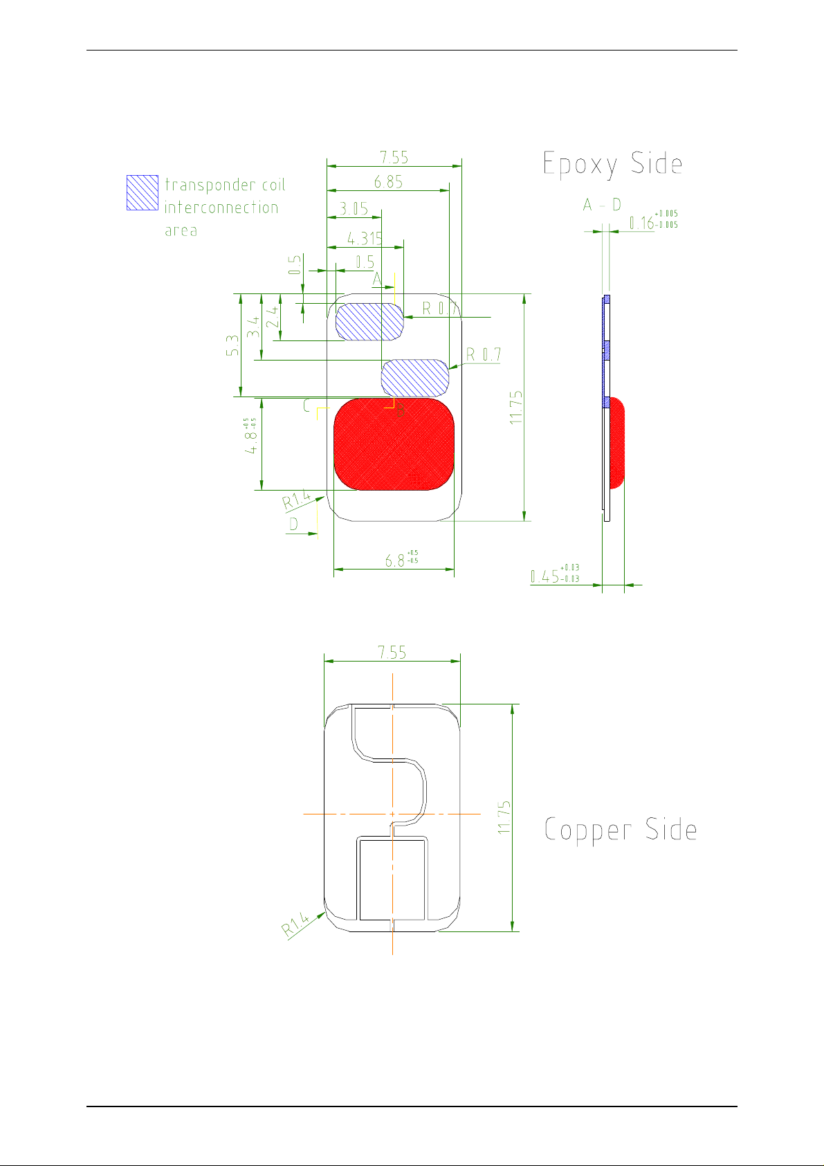
Overall Thickness 0.45 mm ± 0.03 mm
Film Thickness 0.16 mm ± 0.005 mm
Bondpad Size for
Transponder Coil / Module
Interconnection
7.55 mm
11.75 mm see also drawing in chapter 3
1.9 x 3.5 mm Suitable for Welding/Soldering/
Conductive Gluing
2.2 Materials
Tape 110 µm Glass epoxy
Copper Plating 35 µm ED copper
Bond Plating Ni / Au Suitable for Al and Au wire
bonding
Backside Plating Ni / Au
Glob Top Filled Epoxy Thermal curing
2.3 Temperature Range
Operating -25°C to +85°C For packed transponder,
depending on type of package
Processing 150°C for 30 minutes at a standard lamination
pressure for contactless smart
card plastic materials (e.g. PVC,
PET, ...)
Welding Parameters max. 25 ms @ 500 °C on bond pads
Soldering Parameters max. 3 s @ 390 °C on bond pads
Ht1moa3.doc/HS Page 4 of 24
Page 5

Specifications of the HT1 MOA3 S30 Rev. 1.1 1997-08-19
2.4 Storage Conditions
Temperature 15 - 30 °C
Relative Humidity 40 - 70 %
Duration 1 year
2.5 Delivery Conditions
Delivery Identification Date of ready for shipment, reel numbers, total quantity of good
modules with the detail of good modules per reel, order number,
product type, no supplier identification on reels, bags and boxes.
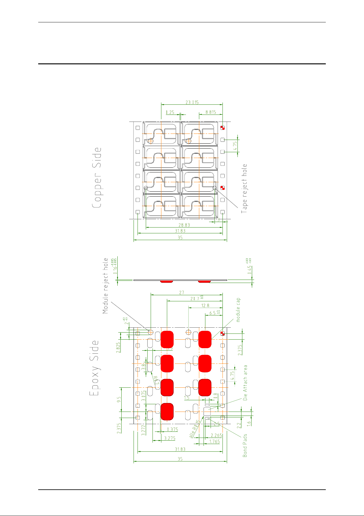
Types of Delivery Chip modules on reel
approx. 15.000 to 20.000
pcs. per reel,
tape width super 35 mm,
pitch 9,5 mm, 2 rows
single chip modules (bulk goods)
Packing and Transport According to documentation
"Packing Method Modules (reel)"
"Packing Method Modules (singulated)"
Bad Module Marking All bad modules (mechanical and
electrical faults) must be punched by
reject hole for customer
Bad positions (reel): <20%
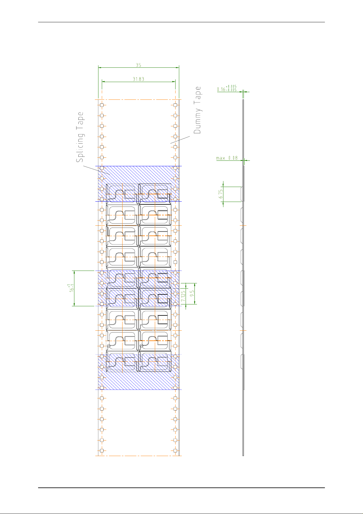
Splicing Specifications Tape material: adhes. tape 15,5 +/- 0,7
mm, thermal resistance at
<190°C by < 100 cN tractive power and
< 30 sec. duration.
Labeling Identification label on the reel and on
carton bag:
- Product type
- Number of the reel
- Total number of positions
- Number of good positions
- Date of sealing (to be checked)
- Two batches per reel only
- Batchnumber indication (only coded,
to be checked)
500 pcs . per bag
Order-No. 3322 845 04881
see drawings chapter 3
see drawings chapter 3
Ht1moa3.doc/HS Page 5 of 24
Page 6

Specifications of the HT1 MOA3 S30 Rev. 1.1 1997-08-19
2.6 Electrical Specifications
Symbol min typ max Comment / Conditions
Absolute Maximum Ratings
Junction Temperature T
Input Peak Current I
J
INpeak
-55°C 140°C
30 mA
Latch up Current 100 mA MIL-STD 883D, Method 3023
ESD 2 kV MIL-STD 883D, Method 3015.7,
Human Body
Operating Range
Temperature T
1)
Input Threshold Voltage
Input Read Voltage
Input Write Voltage
3)
1)
3)
1)
3)
V
V
V
A
IN,TH
IN,RD
IN,WR
-40°C 85°C
3,1 Vp4,2 Vpstart modulation after SETCC
3,5 Vp4,5 Vpread E²PROM
3,7 Vp4,7 Vpwrite E²PROM
R
ThJunctionAmbient
= 30 mA
I
INpeak
≤ 30 K/W @
Demodulator
Range
3)
V
DEM_R
2,0 V
p
4,0 VpV
- V
INHigh
T0=8 µs, T
INLow
MOD
@ V
=6*T
INHigh
0
= 5,0 V
2)
Modulator
R_MOD linear
R_MOD nonlinear
3)
3)
Resonance Capacitor
3)
R
MODL
R
MODNL
4,5 kΩV
3,6 kΩV
INLow
INLow
≤ 2,0 V
≥ 2,0 V
p
p
p
C
ResInit
189 pF 210 pF 231 pF VIN = 4,0 V
EEPROM
Write Current
Read Current
4)
4)
I
W
I
R
25 µA VDD = 2,8 V
9 µA VDD = 2,8 V
Data Retention Years 10 @ 55°C
Write Endurance Cycles 100.000
1)
2)
3)
4)
tested on silicon level
V
IN
INHigh
INLow
MOD
= V
V
V
T
@ Ri = 10
IN1
− V
... voltage between connection pads
IN2
input voltage before modulation
input voltage during modulation
duration of the modulation
resistance of measurement equipment
Ω
k
p
Ht1moa3.doc/HS Page 6 of 24
Page 7
Specifications of the HT1 MOA3 S30 Rev. 1.1 1997-08-19
3 Drawing of the Chip Module HT1 MOA3 S30
3.1 Drawing of the Reel
Ht1moa3.doc/HS Page 7 of 24
Page 8
Specifications of the HT1 MOA3 S30 Rev. 1.1 1997-08-19
3.2 Module outline suggestion
Ht1moa3.doc/HS Page 8 of 24
Page 9
Specifications of the HT1 MOA3 S30 Rev. 1.1 1997-08-19
3.3 Splicing Specification
Ht1moa3.doc/HS Page 9 of 24
Page 10
Specifications of the HT1 MOA3 S30 Rev. 1.1 1997-08-19
4 Coil Specifications
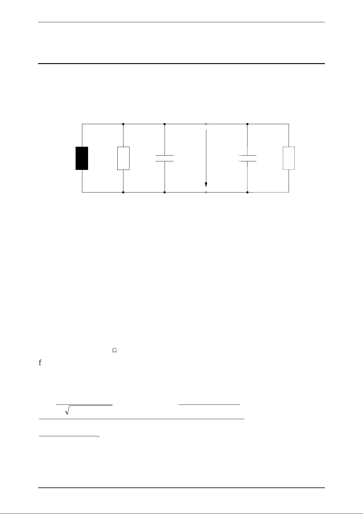
The HITAG 1 chip module has to be connected to a coil whose parameters are briefly described
in the following.
Equivalent circuit of the transponder
U
f
X
R
C
C
R
f
L
L
res
resc
pc
pc
c
pc
pc
p
chip
chip
Xpc Rpc Cp
Uc
... voltage at the connection pads
... resonant frequency of the transponder
... parallel reactance of the coil (f = 125 kHz)
... parallel resistance of the coil (f = 125 kHz)
... parasitic capacitance of the package
... capacitance of the chip (Uc > 4 Vpp)
... resistance of the chip
... self resonant frequency of the coil
=
=
Xpc/2πf (f = 125 kHz)
7.72 mH ± x % (Cp = 0, x depends on the coil production process)
Cchip Rchip
C
R
f
chip
pc
resc
= 210 pF ± 10 %
> 45 k
> 750 kHz
Note: The parasitic capacitance of the package (Cp) must be considered.
=
f
res
2(C C).L
π
1
+
chip p pc
Typical values for C
=⇒
125 kHz L =
p
pc
2f C + C
π
()
1
2
()
res chip p
hot laminated cards: Cp = 1.5 pF
moulded tags: Cp = 6.0 pF
Ht1moa3.doc/HS Page 10 of 24
Page 11

Specifications of the HT1 MOA3 S30 Rev. 1.1 1997-08-19
For a rough estimation ( ± 10 %) of the number of coil windings following formula can be used.
It is assumed that the winding is done in circular form.
N
=
1,85
L
2Uln(
u
)
d
N ... Number of windings
L ... Inductance [nH]
U ... average coil circumference [cm]
d ... copper diameter [mm]
u ... average coil circumference [mm]
For fine tuning a measurement of the inductance and an according adjustment of the number of
windings is necessary. This process always needs some iterations.
Ht1moa3.doc/HS Page 11 of 24
Page 12
Specifications of the HT1 MOA3 S30 Rev. 1.1 1997-08-19
y
y
g
g
g
5 Functional Description of HITAG 1
5.1 Memory Organization
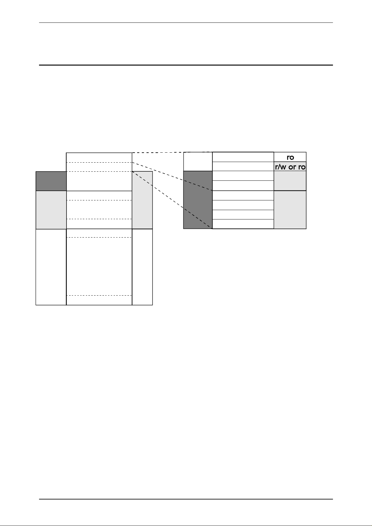
The 2 kBit EEPROM memory on the transponder is divided into 16 blocks.
Every block consists of 4 pages. A page is the smallest access unit.
Every page consists of 4 bytes (at 8 bits).
Block access is only available for Blocks 2-15, page access is available for Pages 0-63.
secret
secret
or
public
public
Block 0
Block 1
user data
Block 4
user data
Block 7
Block 8
user data
Block 15
r/w
or
OTP
r/w
public
Serial Number
Configuration
KeyA
wo or 0
r/w
or
0
secret
ro
r/w
wo
OTP
0
KeyB
Logdata 1B
data 0A
Lo
Lo
data 1A
data 0B
Lo
read onl
read/write
write onl
one time programmable
neither read nor write
Configuration of the memory is
done in the configuration page
Area s (or s etting s) with light d ark bac kgrou nd may be configur ed by the O EM client using t he
Configuration Page (Page 1).
Memory locations marked with "secret" can only be accessed after a mutual aut hentication. An
enciphered data communication is used in that area.
Memory locations marked with "public" can be accessed without mutual authentication, no
encryption is used.
Block 0 includes the unique serial number (programmed during the production process), the
Configuration Page (configuration of the memory area) and the keys, Block 1 includes the
logdata.
Ht1moa3.doc/HS Page 12 of 24
Page 13

Specifications of the HT1 MOA3 S30 Rev. 1.1 1997-08-19
Blocks 4 to 7 can be used either as secret or public areas (configurable), and Blocks 2 to 7 either
as read / write or read only areas (configurable). You can also modify keys and logdata and
prevent them from being accessed.
Finally the Configuration Page itself can be set to read only.
It is extremely important to be particularly careful when using the Configuration Page (it
only can be set to read only once!), keys and logdata as you can lose access to the secret
area on the transponder in case of a mistake.
ATTENTION:
Changing of the Configuration Page (Page 1), Keys and Logdata must be done in secure
environment. The transponder must not be moved out of the communication field of the
antenna during programming! We recommend to put the transponder close to the antenna
(zero-distance) and not to remove it during programming.
5.2 Anticollision
Ant icollision M ode in long rang e applications inclu ding HIT AG 1 tr anspond ers permits you to
process several transponders simultaneously. Theoretically up to 232 transponders can be
pr oce s s e d s imu ltan o usly. I n p r act ic e this n u mb e r is limited , because of the mutual influence of the
transponders - they detune each other, if there are too many too close to each other.
The currently used read/write device must also support full anticollisio n fe atu re (e .g. H TRM800).
For read/write devices without that feature only one transponder is handled even if there are
several transponders within the communication field of the antenna. In this case either no
communication takes place or the "stronger" or closer transponder takes over.
By muting a selected transponder (HALT Mode) another t ransponder that is to be found in the
communication field of the antenna can be recognized.
Ht1moa3.doc/HS Page 13 of 24
Page 14

Specifications of the HT1 MOA3 S30 Rev. 1.1 1997-08-19
5.3 Operation Modes and Configuration
5.3.1 Modes of Operation
The HITAG 1 can be operated in two modes (Standard Protocol Mode, Advanced Protocol
Mode) that cannot be configured using the Configuration Page, but via special host commands.
Advan ced Protocol Mode is not avai lable f or HITAG 1 transponders based on ASIC HT1 ICS30 01x
(only available f or HITAG 1 transponders based on ASIC HT1 ICS30 02x) and uses, above all, an
additional Cyclic Redundancy Check (CRC) for read operations.
5.3.2 Configuration
The Configuration Page consists of 4 Configuration Bytes, the first two bytes are used for
configuration, the other two bytes can be used freely.
The bitmaps in Configuration Bytes 0 and 1 determine the configuration of the memory, i.e. they
define which area is secret or public, read/write, read only, write only or neither read nor write.
You can allocate and write the Configuration Page until it is locked (Bit 4 of Configuration Byte
1 is set to ‘0’).
After that these bytes are read o nly bytes and the configuration of the transponder memory cannot
be changed any more.
ATTENTION: Once set to read only the Configuration Page cannot be changed back to
read/write again (transponder is hardware protected)!
Configuration Bytes 2 and 3: These two bytes, to o, are set to read only by the OEM Lock Bit
(Configuration Byte 1 / Bit 4 = ”0”). Co nsidering that fact you can use these two bytes freely.
They will not affect memory configuration.
Explanations of abbreviations used:
r/w read and write
ro read only
wo write only
0 neither read nor write
Ht1moa3.doc/HS Page 14 of 24
Page 15

Specifications of the HT1 MOA3 S30 Rev. 1.1 1997-08-19
Configuration Byte 0:
1 03 25 47 6
Block 7: "1" ... r/w
"0" ... ro
Block 6: "1" ... r/w
"0" ... ro
Block 5: "1" ... r/w
"0" ... ro
Block 4: "1" ... r/w
"0" ... ro
Block 3: "1" ... r/w
"0" ... ro
Block 2: "1" ... r/w
"0" ... ro
Key A and Key B: "1" ... wo
"0" ... 0
Logdata A and B: "1" ... r/w
"0" ... 0
Configuration Byte 0 / Bit 7:
Bit 7 = ‘1’: Logdata can be read and written to.
Bit 7 = ‘0’: Logdata cannot be accessed.
This bit can be set or reset until Bit 4 of Configuraion Byte 1 is set to ‘0’.
For further information on Logdata and Keys see chapter “Definition of Keys and Logdata“.
Configuration Byte 0 / Bit 6:
Bit 6 = ‘1’: Keys can only be written to.
Bit 6 = ‘0’: Keys cannot be accessed.
This bit can be set or reset until Bit 4 of Configuration Byte 1 is set to ‘0’.
For further information on Logdata and Keys see chapter “Definition of Keys and Logdata“.
Configuration Byte 0 / Bits 0 ... 5:
If one of these Configuration Bits is ‘1’, the corresponding block of the tr ansponder can be read
and written.
If the bit is set to ‘0’, the corresponding block can only be read.
Within one block the configuration is always identical, that means either all 4 pages are read/write
or all of them are read only.
These bits can be set or reset until Bit 4 of Configuration Byte 1 is set to ‘0’.
Ht1moa3.doc/HS Page 15 of 24
Page 16

Specifications of the HT1 MOA3 S30 Rev. 1.1 1997-08-19
Configuration Byte 1:
1 03 25 47 6
Access type for Blocks 4 to 7: "0" ... SECRET
"1" ... PUBLIC
reserved
reserved
reserved
OEM Lock Bit: "0" ... Configuration Page is ro
"1" ... Configuration Page is r/w
reserved
reserved
reserved
Configuration Byte 1 / Bits 5 ... 7:
These three bits are reserved.
ATTENTION: When writing a new value to Configurati on Byt e 1, bit p osition s marked as
“reserved“ must not be altered. To meet that condition read the current Configuration
Byte 1 value and mask in your new values for bit positions you are allowed to change.
Configuration Byte 1 / Bit 4:
Bit 4 = ‘1’: Configuration Page can be read and written to.
Bit 4 = ‘0’: Configuration Page can only be read. This process is irreversible !
ATTENTION: Do not set Bit 4 of Configuration Byte 1 to ‘0’ before having written the
final data into the Configuration Page of the transponder.
Configuration Byte 1 / Bits 1 ... 3:
These three bits are reserved.
ATTENTION: When writing a new value to Configurati on Byt e 1, bit p osition s marked as
“reserved“ must not be altered. To meet that condition read the current Configuration
Byte 1 value and mask in your new values for bit positions you are allowed to change.
Configuration Byte 1 / Bit 0:
Bit 0 = ‘0’: Access type for Blocks 4 to 7 is SECRET.
Bit 0 = ‘1’: Access type for Blocks 4 to 7 is PUBLIC.
This bit can be set or reset until Bit 4 of Configuration Byte 1 is set to ‘0’.
Ht1moa3.doc/HS Page 16 of 24
Page 17

Specifications of the HT1 MOA3 S30 Rev. 1.1 1997-08-19
5.4 Configuration of Delivered HITAG 1 Transponders
HITAG 1 transponders are delivered with the following configuration by Philips Semiconductors:
Unique Serial Number:
Serial Number: Read Only - fixed
Configuration Byte 0:
Logdata: ‘1’ = r/w - can be changed
Key A, Key B: ‘1’ = wo - can be changed
Blocks 2 - 7: ‘1’ = r/w - can be changed
Configuration Byte 1:
OEM Lock Bit: ‘1’ = Configuration Page is r/w - can be changed
Blocks 4 - 7: ‘1’ = public - can be changed
Value for Transport Keys, Transport Logdata:
0x00000000
RECOMMENDATION:
Before delivering transponders to end users, the Configuration Page should be set t o read o nly
(Configuration Byte 1/Bit 4 = ‘0’).
5.5 Definition of Keys and Logdata
In order to be able to read dat a from the secret area o f a transponder, you have to carry out a
procedure called authentication. To do this you need special data (keys).
After transmitting the according command the authentication is automatically carried out by the
read/write device.
Keys are cryptographic codes, which determine data encryption during data transfer between
read/write device and transponder.
Two keys (Key A and Key B) which you can use independently of each other, have been installed
fo r security an d fle xib ility rea s ons. The ide n tity o f e ither K e y A o r Key B on t he read/writ e dev ic e
and on the transponder is sufficient.
Logdata represent "passwo rds" needed to gain access to secr et areas on the tr ansponder. A pair
of logdata is included with every cryptographic key (Key A and Key B). T his logdata pair has t o
be identical both on the transponder and the read/write device.
ad Key A: Logdata 0 A "Password" which t he t r ansponder sends to
Logdata 1 A "Password" which the read/write device
ad Key B: Logdata 0 B and
Logdata 1 B analogous to Key A
Ht1moa3.doc/HS Page 17 of 24
the read/write device and which is verified
by the latter.
sends to the transponder and which is
checked for iden ti ty by the latter.
Page 18

Specifications of the HT1 MOA3 S30 Rev. 1.1 1997-08-19
It is important t hat t he following values are in accordance with each other, i.e. t he respect ive data
on the read/write device and on the transponder have to be identical pairs:
on the
read/write
on the
transponder
device
KEY A
LOGDATA 0A
LOGDATA 1A
KEY B
LOGDATA 0B
LOGDATA 1B
⇔
⇔
⇔
⇔
⇔
⇔
KEY A
LOGDATA 0A
LOGDATA 1A
KEY B
LOGDATA 0B
LOGDATA 1B
Set A
Set B
The keys and log dat a are predefined by P hilips Semico nduc tors by me ans o f defined Trans por t
Keys (both keys show the same bit map) and Transport Logdata (all logdata show the same bit
map), see also chapter “Configuration of Delivered HITAG 1 Transponders“.
They can be written to, which means that they can be changed.
ATTENTION: Keys and Logdata only can be changed if their current values are known!
Ht1moa3.doc/HS Page 18 of 24
Page 19

Specifications of the HT1 MOA3 S30 Rev. 1.1 1997-08-19
6 Quality Inspection
Quality inspection is performed with statistical quality control according to ISO 2859 part 1, with
AQL1.0.
Optical Properties scratches,
encapsulation failures,
gold discolouration,
delamination
Geometrical Properies width measured with gauge
length measured with gauge
overall thickness measured with micrometer at the center of
Electrical Properties operation basic read/write operations
Shipment Quantity
Packing and Labeling
according to the reference sample
catalogue
the glob top
Ht1moa3.doc/HS Page 19 of 24
Page 20

Specifications of the HT1 MOA3 S30 Rev. 1.1 1997-08-19
7 Characterisation and Test of the Final Transponder
7.1 Characterisation of the Transponder
The parameters recommended to be characterised for the transponder are:
Parameter Comment
Resonant frequency f
Threshold value B
Threshold value for READ B
Threshold value for WRITE B
res
TH
RD
WR
Transponder does not modulate
Resonant frequency @ T
Start of modulation
Command READ_PAGE OK
Command WRITE_PAGE OK
= 22°C, @ B
amb
TH
For the measurement of these parameters we recommend to use the test equipment available from
SCEMTEC, Marienheide-Rodt, Germany (Transponder Measurement System STM-1).
This device also supports functional testing (besides parameter testing). Therefore it can also be
used as production test equipment for the final transponder test. For further information please
contact Scemtec GmbH.
7.2 Final Test of the Transponder
In addition to the equipment described in the previous chapter Philips Semiconductors offers a
device for a final functional test of transponders, the HITAGTM Test System HT OT490.
Parameter tests are not supportet by this device.
Basic flow for production and test:
1. Assembly of transponders
2. Functional test and final test of the EEPROM
Since the Keys and Logdata are changed during final test the Configuration and
personalization must take place after the final test. The final test is disabled (not reversible)
by setting the Tag-test mode bit to 0.
For the final test of transponders we recommend to use the
TM
HITAG
Test System HT OT490 of Philips Semiconductors or the
Transponder Measurement System STM-1 of Scemtec.
Ht1moa3.doc/HS Page 20 of 24
Page 21

Specifications of the HT1 MOA3 S30 Rev. 1.1 1997-08-19
8 Ordering Information
Type Name Description Ordering Number
HT1 MOA3 S30/E/3 HITAG 1 S30 Chip Module, reels 9352 600 61118
HT1 MOA3 S30/E/1 HITAG 1 S30 Chip Module, bulk
9352 602 18122
Ht1moa3.doc/HS Page 21 of 24
Page 22

Specifications of the HT1 MOA3 S30 Rev. 1.1 1997-08-19
Definitions
Data sheet status
Objective specificationThis data sheet conta ins ta rget o r goal specific ations for product deve lopment.
Preliminary specificationThis data s heet conta ins preliminary data; s upp lementary data may be
published later.
Product spec ification This data sheet conta ins final product spec ifications.
Limiting values
Limiting values given are in acco rdance with the Abso lute Maximum Rating Syste m (IEC 134).
Stress above one o r more of the limiting values may cause pe rmanent da mage to the dev ice.
These are stres s ratings on ly and ope ration of the device at these o r at any othe r conditions
above those g iven in the Characteristics sect ion of the spec ification is not implied. Expos u re to
limiting values for extended pe riods may affect dev ice reliability.
Application information
Where application information is given, it is advisory and does not form part of the spec ification.
Life support applications
These products are not designed for use in life support appliances, devices, or systems where
malfunction of these products can reasonably be expected to result in personal injury. Philips
Semiconductors´ customers using or selling these products for use in such applications do so on
their own risk and agree to fully indemnify Philips Semiconductors for any damages resulting from
such improper use or sale.
Ht1moa3.doc /HS Page 22 of 24
Page 23

Specifications of the HT1 MOA3 S30 Rev. 1.1 1997-08-19
- this page intentionally left blank -
Ht1moa3.doc/HS Page 23 of 24
Page 24

Philips Semiconductors - a worldwide company
Argentina
Australia
Tel. +612 9805 4455, Fax. +612 9805 4466
Austria
Tel. +431 60 101, Fax. +431 30 101 1210
Belarus
220050 MINSK, Tel. +375172 200 733, Fax. +375172 200 773
Belgium
Brazil
Bulgaria
51 James Bourchier Blvd., 1407 SOFIA Tel. +4822 612 2831, Fax. +4822 612 2327
Tel. +3592 689 211, Fax. +3592 689 102
Canada
Tel. +1800 234 7381
China/Hong Kong
72 Tat Chee Avenue, Kowloon Tong, HONG KONG,
Tel. +85223 19 7888, Fax. +85223 19 7700 Tel. +65350 2538, Fax. +65251 6500
Colombia
Czech Republic
Denmark
Tel. +4532 88 2636, Fax. +4531 57 1949 2092 JOHANNESBURG, P.O.Box 7430 Johannesburg 2000,
Finland
Tel. +3589 61 5800, Fax. +3589 61 580/xxx
France
Tel. +331 40 99 6161, Fax. +331 40 99 6427 Tel. +5511 821 2333, Fax. +5511 829 1849
Germany
Tel. +4940 23 53 60, Fax. +4940 23 536 300 Tel. +343 301 6312, Fax. +343 301 4107
Greece
Tel. +301 4894 339/239, Fax. +301 4814 240 Tel. +468 632 2000, Fax. +468 632 2745
Hungary
India
Worli, MUMBAI 400018, Tel. +9122 4938 541, Fax. +9122 4938 722
Indonesia
Ireland
Tel. +3531 7640 000, Fax. +3531 7640 200
Israel
Tel. +9723 645 0444, Fax. +9723 649 1007 Tel. +662 745 4090, Fax. +662 398 0793
Italy
20124 MILANO, Tel. +392 6752 2531, Fax. +392 6752 2557 Tel. +90212 279 2770, Fax. +90212 282 6707
Japan
Tel. +813 3740 5130,Fax. +813 3740 5077 252042 KIEV, Tel. +38044 264 2776, Fax. +38044 268 0461
Korea
Tel. +822 709 1412, Fax. +822 709 1415 MIDDLESEX UM3 5BX, Tel. +44181 730 5000, Fax. +44181 754 8421
Malaysia
Tel. +60 3750 5214, Fax. +603 757 4880 Tel. +1800 234 7381
Mexico
Tel. +9 5800 234 7381
Middle East
: see South America
: 34 Waterloo Road, NORTHRYDE, NSW 2113, Tel. +3140 27 82785, Fax +3140 27 88399
: Computerstraße 6, A-1101 WIEN, P.O.Box 213, Tel. +649 849 4160, Fax. +649 849 7811
: Hotel Minsk Business Centre, Bld. 3, r.1211, Volodarski Str. 6, Tel. +4722 74 8000, Fax. +4722 74 8341
: see The Netherlands 106 Valero St. Salcedo Village, P.O.Box 2108 MCC, MAKATI,
: see South America Metro MANILA, Tel. +632 816 6380, Fax. +632 817 3474
: Philips Bulgaria Ltd., Energoproject, 15th floor,
: Philips Semiconductors/Components,
: 501 Hong Kong Industrial Technology Centre, Tel. +7095 247 9145, Fax. +7095 247 9144
: see South America
: see Austria
: Prags Boulevard 80, PB 1919, DK-2300 COPENHAGEN S,
: Sinikalliontie 3, FIN-02630 ESPOO, Tel. +2711 470 5911, Fax. +2711 470 5494
: 4 Rue du Port-aux-Vins, BP 317, 92156 SURESNES Cedex, 04547-130 Sao Paulo, SAO PAULO - SP, Brazil,
: Hammerbrookstraße 69, D-20097 HAMBURG,
: No. 15, 25th March Street, GR 17778 TAVROS/ATHENS,
: see Austria
: Philips INDIA Ltd., Shivsagar Estate, A Block, Dr. Annie Besant Rd. Tel. +411 488 2686, Fax. +411 481 7730
: see Singapore Chung Hsiao West Road, Sec. 1, P.O.Box 22978,
: Newstead, Clonskeagh, DUBLIN 14, TAIPEI 100, Tel. +8862 382 4443, Fax. +8862 382 4444
: RAPAC Electronics, 7 Kehilat Saloniki St., TEL AVIV 61180, 209/2 Sanpavuth-Bangna Road Prakanong, BANGKOK 10260,
: Philips Semiconductors, Piazza IV Novembre 3,
: Philips Bldg. 13-37, Kohnan 2-chome, Minato-ku, TOKYO 108,
: Philips House, 260-199, Itaewon-dong, Yonsan-ku, SEOUL,
: No. 76 Jalan Universiti, 46200 PETALING JAYA, Selangor,
: 5900 Gateway East, Suite 200, EL PASO, Texas 79905,
: see Italy
Netherlands
New Zealand
Norway
Philippines
Poland
Portugal
Romania
Russia
Singapore
Slovakia
Slovenia
South Africa
South America
Spain
Sweden
Switzerland
Taiwan
Thailand
Turkey
Ukraine
United Kingdom
United States
Uruguay
Vietnam
Yugoslavia
Tel. +38111 625 344, Fax. +38111 635 777
: Postbus 90050, 5600 PB EINDHOVEN, Bldg. VB,
: 2 Wagener Place, C.P.O. Box 1041, AUCKLAND,
: Box 1, Manglerud 0612, OSLO,
: Philips Semiconductors Philippines Inc.,
: Ul. Lukiska 10, PL 04-123 WARSZWA,
: see Spain
: see Italy
: Philips Russia, Ul. Usatcheva 35A, 119048 MOSCOW,
: Lorong 1, Toa Payoh, SINGAPORE 1231,
: see Austria
: see Italy
: S.A. Philips Pty Ltd., 195-215 Main Road Martindale,
: Al. Vicente Pinzon, 173 - 6th floor,
: Balmes 22, 08007 BARCELONA,
: Kottbygatan 7, Akalla, S-16485 STOCKHOLM,
: Allmendstraße 140, CH-8027 ZÜRICH,
: Philips Taiwan Ltd., 2330F, 66,
: Philips Electronics (Thailand) Ltd.,
: Talapasa Cad. No. 5, 80640 GÜLTEPE/ISTANBUL,
: Philips Ukraine, 4 Patrice Lumumba Str., Building B, Floor 7,
: Philips Semiconductors Ltd., 276 Bath Road, Hayes,
: 811 Argues Avenue, SUNNYVALE, CA94088-3409,
: see South America
: see Singapore
: Philips, Trg N. Pasica 5/v, 11000 BEOGRAD,
Philips Semiconductors, Mikron-Weg 1, A-8101 Gratkorn, Austria Fax: +43 / 3124 / 299 - 270
For all other countries apply to
Building BE-p, P.O.Box 218, 5600 MD EINDHOVEN, The Netherlands, Fax: +3140 27 24825
© Philips Electronics N.V. 1996 SCB52
All rights are reserved. Reproduction in whole or in part is prohibited without the prior written consent of the copyright owner.
The information presented in this document does not form part of any quotation or contract, is believed to be accurate and reliable and may be changed without any
notice. No liability will be accepted by the publisher for any consequence of its use. Publication thereof does not convey nor imply any license under patent- or other
industrial or intellectual property rights.
: Philips Semiconductors, Marketing & Sales Communications, Internet: http://www.semiconductors.philips.com
 Loading...