

Datasheet 16TTS12STRR, 16TTS12STPL, 16TTS08STRR, 16TTS08STRL Datasheet (International Rectifier)
Page 1
1
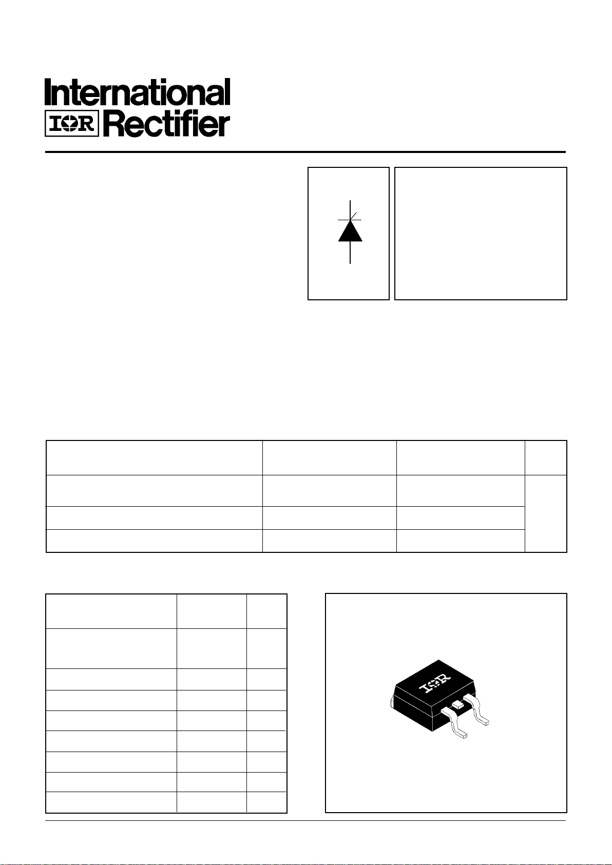
SURFACE MOUNTABLE
PHASE CONTROL SCR
Bulletin I2105
16TTS..S SERIES
V
T
< 1.4V @ 10A
I
TSM
= 200A
VR/ VD= 1200V
Major Ratings and Characteristics
D2 PAK (SMD-220)
I
T(AV)
Sinusoidal 10 A
waveform
I
RMS
16 A
V
RRM
/
V
DRM
800 and 1200 V
I
TSM
200 A
V
T
@ 10 A, TJ = 25°C 1.4 V
dv/dt 500 V/µs
di/dt 150 A/µs
T
J
- 40 to 125 °C
Characteristics 16TTS..S Units
Output Current in Typical Applications
TA = 55°C, TJ = 125°C, footprint 300mm
2
NEMA FR-4 or G10 glass fabric-based epoxy
2.5 3.5
with 4 oz (140µm) copper
Aluminum IMS, R
thCA
= 15°C/W 6.3 9.5 A
Aluminum IMS with heatsink, R
thCA
= 5°C/W 14.0 18.5
Applications Single-phase Bridge Three-phase Bridge Units
Description/Features
The 16TTS..S new series of silicon controlled
rectifiers are specifically designed for medium
power switching and phase control applications.
The glass passivation technology used has reliable operation up to 125° C junction temperature.
Typical applications are in input rectification (soft
start) and these products are designed to be used
with International Rectifier input diodes, switches
and output rectifiers which are available in identical package outlines.
Page 2
2
16TTS.. S Series
Part Number
V
RRM
, maximum V
DRM
, maximum I
RRM/IDRM
peak reverse voltage peak direct voltage 125°C
VVmA
16TTS08S 800 800 5
16TTS12S 1200 1200
V oltage Ratings
I
T(AV)
Max. Average On-state Current 10 A 50% duty cycle @ TC = 98° C, sinusoidal wave form
I
RMS
Max. RMS On-state Current 16
I
TSM
Max. Peak One Cycle Non-Repetitive 170 10ms Sine pulse, rated V
RRM
applied
Surge Current 200 10ms Sine pulse, no voltage reapplied
I2t Max. I2t for fusing 144 A2s 10ms Sine pulse, rated V
RRM
applied
200 10ms Sine pulse, no voltage reapplied
I2√t Max. I2√t for fusing 2000 A2√s t = 0.1 to 10ms, no voltage reapplied
V
TM
Max. On-state Voltage Drop 1.4 V @ 10A, TJ = 25°C
r
t
On-state slope resistance 24.0 mΩ TJ = 125°C
V
T(TO)
Threshold Voltage 1.1 V
IRM/IDMMax.Reverse and Direct 0.5 mA TJ = 25 °C
Leakage Current 5.0 TJ = 125 °C
I
H
Max. Holding Current 100 mA Anode Supply = 6V, Resistive load, Initial IT=1A
I
L
Max. Latching Current 200 mA Anode Supply = 6V, Resistive load
dv/dt Max. rate of rise of off-state Voltage 500 V/µs
di/dt Max. rate of rise of turned-on Current 150 A/µs
Absolute Maximum Ratings
Parameters 16TTS..S Units Conditions
VR = rated V
RRM
/ V
DRM
Page 3
3
16TTS.. S Series
Triggering
P
GM
Max. peak Gate Power 8.0 W
P
G(AV)
Max. average Gate Power 2.0
+ IGMMax. paek positive Gate Current 1.5 A
- VGMMax. paek negative Gate Voltage 10 V
I
GT
Max. required DC Gate Current 90 mA Anode supply = 6V, resistive load, TJ = - 10°C
to trigger 60 Anode supply = 6V, resistive load, TJ = 25°C
35 Anode supply = 6V, resistive load, TJ = 125°C
V
GT
Max. required DC Gate Voltage 3.0 V Anode supply = 6V, resistive load, TJ = - 10°C
to trigger 2.0 Anode supply = 6V, resistive load, TJ = 25°C
1.0 Anode supply = 6V, resistive load, TJ = 125°C
V
GD
Max. DC Gate Voltage not to trigger 0.25 TJ = 125°C, V
DRM
= rated value
I
GD
Max. DC Gate Current not to trigger 2.0 mA TJ = 125°C, V
DRM
= rated value
Parameters 16TTS..S Units Conditions
Switching
Parameters 16TTS..S Units Conditions
t
gt
Typical turn-on time 0.9 µs TJ = 25°C
t
rr
Typical reverse recovery time 4 TJ = 125°C
t
q
Typical turn-off time 110
T
J
Max. Junction Temperature Range - 40 to 125 °C
T
stg
Max. Storage Temperature Range - 40 to 125 °C
Soldering Temperature 2 40 °C for 10 seconds (1.6mm from case)
R
thJC
Max. Thermal Resistance Junction 1.3 °C/W DC operation
to Case
R
thJA
Typ. Thermal Resistance Junction 40 °C/W
to Ambient (PCB Mount)**
wt Approximate Weight 2 (0.07) g (oz.)
T Case Style D2 Pak (SMD-220)
Thermal-Mechanical Specifications
Parameters 16TTS..S Units Conditions
**When mounted on 1" square (650mm2) PCB of FR-4 or G-10 material 4 oz (140µm) copper 40°C/W
For recommended footprint and soldering techniques refer to application note #AN-994
Page 4

4
16TTS.. S Series
Fig. 2 - Current Rating Characteristics
Fig. 3 - On-state Power Loss Characteristics
Fig. 4 - On-state Power Loss Characteristics
Fig. 6 - Maximum Non-Repetitive Surge Current
Fig. 7 - Maximum Non-Repetitive Surge Current
Fig. 1 - Current Rating Characteristics
90
95
100
105
110
115
120
125
024681012
30°
60°
90°
120°
180°
Conduction Angle
Average On-state Current (A)
Maximum Allowable Case Temperature (°C)
16TTS.. Series
R (DC) = 1.3 K/W
thJC
90
95
100
105
110
115
120
125
0246810121416
DC
30°
60°
90°
120°
180°
Maximum Allowable Case Temperature (°C)
Conduction Period
Average On-state Current (A)
16TTS.. Series
R (DC) = 1.3 K/W
thJ C
0
5
10
15
20
024681012
RMS Limit
180°
120°
90°
60°
30°
Conduction Angle
Average On-state Current (A)
Maximum Average On-state Power Loss (W)
16TTS..
T = 125°C
J
0
5
10
15
20
25
0 2 4 6 8 10 12 14 16 18
DC
180°
120°
90°
60°
30°
RMS Limit
Conduction Period
Average On-state Current (A)
Maximum Average On-state Power Loss (W)
16TTS..
T = 125°C
J
80
100
120
140
160
180
1 10 100
Number Of Equal Amplitude Half Cycle Current Pulses (N)
At Any Rated Load Condition And With
Ra ted V App lied Followi ng Surge.
Initial T = 125°C
@ 60 Hz 0.0083 s
@ 50 Hz 0.0100 s
RRM
J
Peak Half Sine Wave On-state Current (A)
16TTS..Series
60
80
100
120
140
160
180
200
220
0.01 0.1 1 10
Pulse Train Duration (s)
Maximum Non Repetitive Surge Current
Peak Half Sine Wave Forward Current (A)
Versus Pulse Train Duration.
Initial T = 125°C
No Voltage Reapplied
Rated V Reapplied
J
RRM
16TTS.. Series
Page 5

5
16TTS.. S Series
Fig. 7 - On-state Voltage Drop Characteristics
Fig. 8 - Gate Characteristics
Fig. 9 - Thermal Impedance Z
thJC
Characteristics
1
10
100
1000
012345
T = 25°C
J
T = 125°C
J
Instantaneous On-state Voltage (V)
Instantan eous On-state Current (A)
16TTS.. Series
0.1
1
10
100
0.001 0.01 0.1 1 10 100
(b)
(a)
Rectangular gate pulse
(4) (3) (2) (1)
Instantaneous Gate Current (A)
Instan taneous Gate Voltage (V)
TJ = 25 °C
TJ = 125 °C
b)Recommended load line for
VGD
IGD
Frequency Limited by PG(AV)
a)Recommended load line for
rated di/dt: 10 V, 20 ohms
tr = 0.5 µs, tp >= 6 µs
<= 30% rated di/ dt: 10 V, 65 ohms
tr = 1 µs, tp >= 6 µs
(1) PGM = 40 , tp = 1 ms
(2) PGM = 20 W, tp = 2 ms
(3) PGM = 8 W, tp = 5 ms
(4) PGM = 4 W, tp = 10 ms
TJ = -10 °C
16T TS..
0.01
0.1
1
10
0.0001 0.001 0.0 1 0.1 1
Square Wave Pulse Duration (s)
thJC
Steady State Value
(DC Operation)
Transient Therm al Impedance Z (K/W)
16TTS.. Series
Single Pulse
D = 0.50
D = 0.33
D = 0.25
D = 0.17
D = 0.08
Page 6

6
16TTS.. S Series
9G3A
16TTS12S
9512
EXAMPLE: THIS IS AN 16TTS12S
INTERNATIONAL
RECTIFIER LOGO
PART NUMBER
Marking Information
DATE CODE (YYWW)
YY = YEAR
WW = WEEK
ASSEMBLY
LOT CODE
Tape & Reel Information
Dimensions in millimeters and inches
TR R
FEED DIR ECTION
TRL
FEED DIRECTION
10.90 (0.429)
10.70 (0.421)
16.10 (0.634)
15.90 (0.626)
1.7 5 ( 0. 069)
1.2 5 ( 0. 049)
1. 85 ( 0.073)
1. 65 ( 0.065)
4. 10 (0. 161)
3. 90 (0. 153)
1.6 0 ( 0. 063)
1.5 0 ( 0. 059)
DIA.
1.60 (0.063)
1.50 (0.059)
DIA.
11.60 (0.457)
11.40 (0.449)
15.42 (0.609)
15.22 (0.601)
4.7 2 ( 0. 186)
4.5 2 ( 0. 178)
24. 30 (0. 957)
23. 90 (0. 941)
0.368 (0.0145)
0.342 (0.0135)
360 ( 14.173 )
DIA. MAX.
26.40 (1.039)
24.40 (0.961)
13.50 (0.532)
12.80 (0.504)
DIA.
60 (2.362)
DIA. MIN.
SM D-220 Tape & Reel
When ordering, indicate the part
number, part orientation, and the
quantity. Qu antities are in multiples
of 800 pieces per reel f or both
TR L and TRR.
(K) (G)
(A)
Page 7

7
16TTS.. S Series
Outline Table
(K) (G)
1 (K) Cathode
2 (A) Anode
3 (G) Gate
(A)
10.1 6 ( 0.4 0)
REF.
8.89 (0.35)
4.57 (0.18)
4.32 (0.17)
0.61 (0.02) MAX.
5. 08 (0.20) REF.
1.32 (0.05)
1.22 (0.05)
13
6.47 (0.25)
6.18 ( 0.24)
93°
REF.
2.61 (0.10)
2.32 (0.09)
5.28 (0.21)
4.78 (0.19)
4.69 (0.18)
4.20 ( 0.16)
0.55 (0.02)
0.46 (0.02)
14.73 (0.58)
15.49 (0.61)
1.40 (0.055)
1.14 (0.045)
3X
0.93 (0.37)
0.69 (0.27)
2X
11.43 (0.45)
17.78 (0.70)
8.89 (0.35)
3.81 ( 0.15)
2.08 (0.08)
2X
2.54 (0.10)
2X
MINIMU M R E C OMME N D E D F OOT P R IN T
2
16 T T S 12 S TRL
Device Code
1 5243
Ordering Information Table
6
1 - Current Rating, RMS value
2 - Circuit Configuration
T = Single Thyristor
3 - Package
T = TO-220AC
4 - Type of Silicon
S = Converter Grade
5 - Voltage code: Code x 100 = V
RRM
6 - S = TO-220 D2Pak (SMD 220) Version
7 - Tape and Reel Option
TRL = Left Reel
TRR = Right Orientation Reel
08 = 800V
12 = 1200V
Dimensions in millimeters and inches
(G) 3
2
(A)
1 (K)
 Loading...