

Page 1
查询MPC17550供应商
Freescale Semiconductor, Inc.
MOTOROLA
SEMICONDUCTOR TECHNICAL DATA
Document order number: MPC17550
Rev 1.0, 03/2004
Advance Information
17550
Quad H-Bridge Micromotor Driver
with DC/DC Boost Converter
The 17550 is a monolithic quad H-Bridge power IC ideal for portable
electronic applications containing tiny bipolar stepper motors and/or brush
DC-motors powered by two-to-four cell NiCd/NiMH batteries.
The 17550 operates from 2.5 V to 5.5 V, with independent control of each
H-Bridge via parallel 3.0 V or 5.0 V logic-compatible I/O. The device features
an on-board DC/DC boost converter that allows motor operation all the way
down to 1.6 V (the boost converter supplies the gate-drive voltage for each of
the four independent H-bridge output stages). Each output bridge has its own
gate-drive and logic circuitry with built-in shoot-through current protection.
nc...
I
The 17550 has four operating modes: Forward, Reverse, Brake, and
Tri-Stated (High Impedance). The 17550 has a low total R
@ 25°C. In addition, it can be set into a very low current-drain standby mode.
The H-Bridge outputs can be independently PWM’ed at up to 200 kHz for
speed/torque and current control. The 17550 can efficiently drive many types
of micromotors owing to its low output resistance and high output slew rates.
DS(ON)
of 1.2 Ω max
QUAD H-BRIDGE MICROMOTOR
DRIVER WITH DC/DC BOOST
CONVERTER
EV (Pb-FREE) SUFFIX
CASE 1522-01
36-LEAD VMFP
cale Semiconductor,
Frees
Features
• Low Total R
• Output Current 700 mA (Continuous per Output)
• Shoot-Through Current Protection Circuit
• PWM Control Input Frequency up to 200 kHz
• Built-In DC/DC Boost Converter
• Low Power Consumption Standby Mode
• Undervoltage Detection and Shutdown Circuit
• Pb-Free Packaging Designated by Suffix Code EV
0.7 Ω (Typ), 1.2 Ω (Max) @ 25°C
DS(ON)
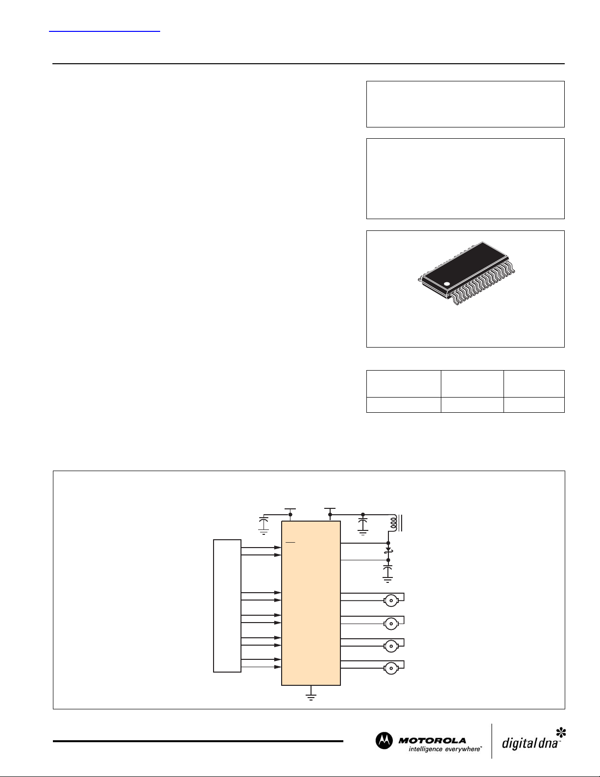
17550 Simplified Application Diagram
MCU
Simplified Application Diagram
V
M
VM
OE
PSB
INAF
INAR
INBF
INBR
INCF
INCR
INDF
INDR
17550
GND
V
V
DD
LX
VG
HBAF
HBAR
HBBF
HBBR
HBCF
HBCR
HBDF
HBDR
DD
ORDERING INFORMATION
Device
MPC17550EV/EL -10°C to 60°C 36 VMFP
Temperature
Range (T
)
A
Package
This document contains certain information on a new product.
Specifications and information herein are subject to change without notice.
© Motorola, Inc. 2004
For More Information On This Product,
Go to: www.freescale.com
Page 2
Freescale Semiconductor, Inc.
GND
V
DD
PSB
INAF
INAR
nc...
I
INBF
INBR
LX VG
DC/DC
Converter
V
DD
VG
V
DD
V
DD
HBA
HBB
AGND
VMA
HBAF
HBAR
PGND
VMB
HBBF
cale Semiconductor,
Frees
OE
INCF
INCR
INDF
INDR
HBBR
V
DD
Control
Logic
Gate
Driver
and
Level
Shifter
PGND
HBC
VMC
HBCF
HBCR
PGND
HBD
VMD
HBDF
HBDR
PGND
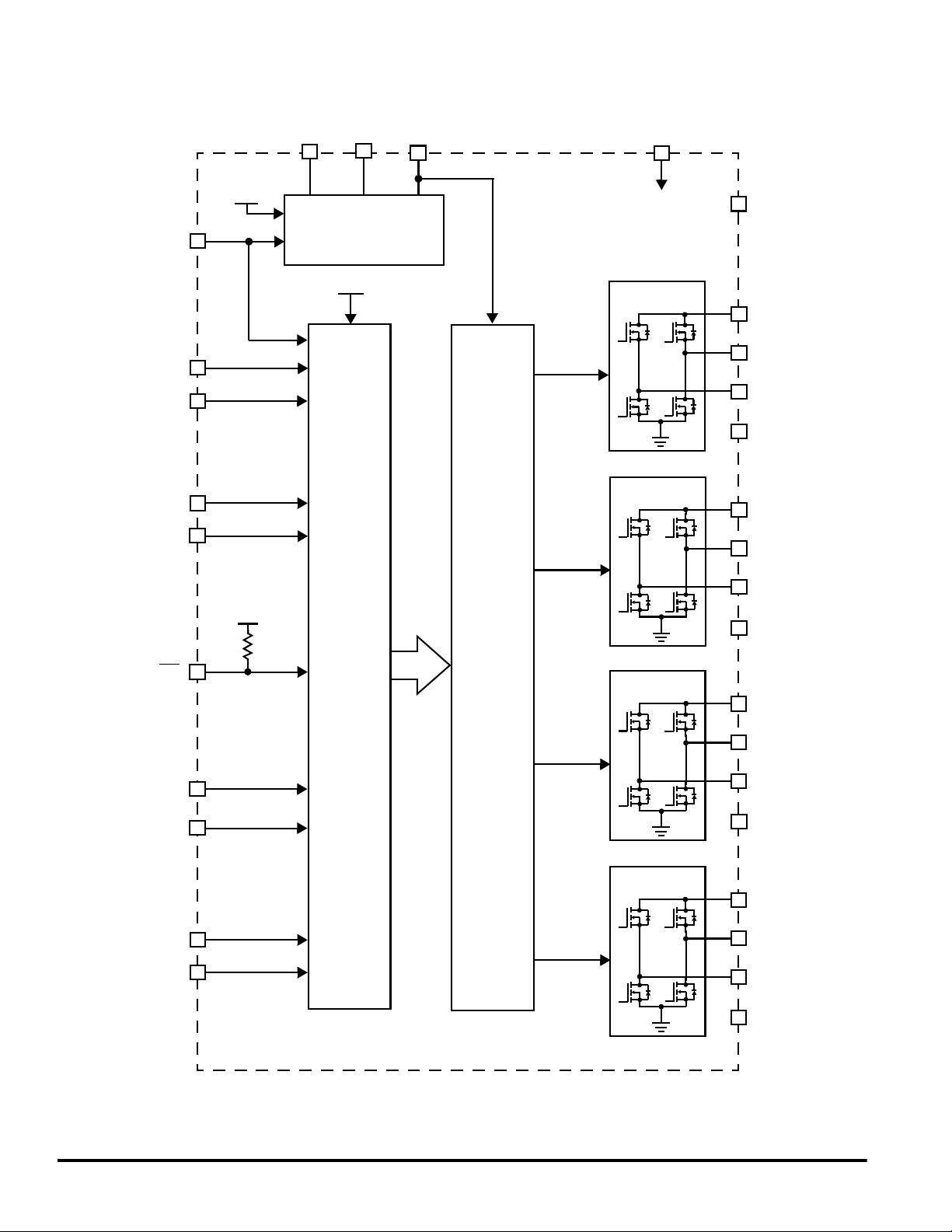
Figure 1. 17550 Simplified Internal Block Diagram
17550 MOTOROLA ANALOG INTEGRATED CIRCUIT DEVICE DATA
2
For More Information On This Product,
Go to: www.freescale.com
Page 3
Freescale Semiconductor, Inc.
nc...
I
cale Semiconductor,
Frees
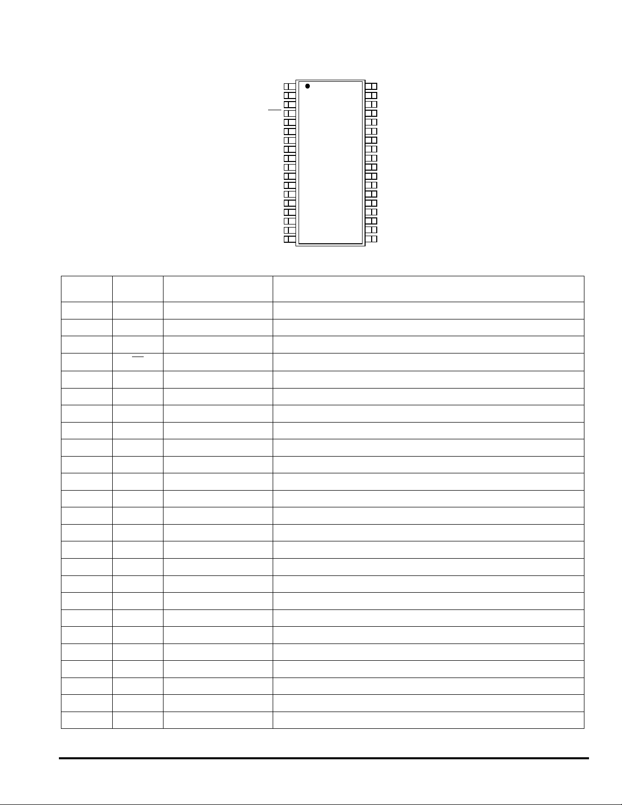
TERMINAL FUNCTION DESCRIPTION
Terminal
1 AGND Analog Ground
2 NC No Connect
3 PSB Power Standby
4 OE Output Enable
5, 9
6 HBAF HBA Forward Output
8 HBAR HBA Reverse Output
10, 14 VMB Motor Drive Power Supply B
11 HBBR HBB Reverse Output
7, 12, 25, 30 PGND Power Ground
13 HBBF HBB Forward Output
15 INAR Input Control HBA Reverse
16 INAF
17 INBF Input Control HBB Forward
18 INBR Input Control HBB Reverse
19 INDR Input Control HBD Reverse
20 INDF Input Control HBD Forward
21 INCF Input Control HBC Forward
22 INCR Input Control HBC Reverse
23, 27 VMD Motor Drive Power Supply D
24 HBDF HBD Forward Output
26 HBDR HBD Reverse Output
28, 32 VMC Motor Drive Power Supply C
29 HBCR HBC Reverse Output
31 HBCF HCB Forward Output
Terminal
Name
VMA Motor Drive Power Supply A
Formal Name Definition
Input Control HBA Forward Control signal input for H-Bridge A forward.
AGND
NC
PSB
OE
VMA
HBAF
PGND
HBAR
VMA
VMB
HBBR
PGND
HBBF
VMB
INAR
INAF
INBF
INBR
1
2
3
4
5
6
7
8
9
10
11
12
13
14
15
16
17
18
Analog and logic signal ground reference terminal.
No connection to this terminal.
Power standby mode control terminal.
Logic output Enable control of H-Bridges (Low = True).
Power supply voltage connection for Motor “A” (top of HBA).
Forward output of H-Bridge A.
Reverse output of H-Bridge A.
Power supply voltage connection for Motor “B” (top of HBB).
Reverse output of H-Bridge B.
Power ground connection.
Forward output of H-Bridge B.
Control signal input for H-Bridge A reverse.
Control signal input for H-Bridge B forward.
Control signal input for H-Bridge B reverse.
Control signal input for H-Bridge D reverse.
Control signal input for H-Bridge D forward.
Control signal input for H-Bridge C forward.
Control signal input for H-Bridge C reverse.
Power supply voltage connection for Motor “D” (top of HBD).
Forward output of H-Bridge D.
Reverse output of H-Bridge D.
Power supply voltage connection for Motor “C” (top of HBC).
Reverse Output of H-Bridge C.
Forward Output of H-Bridge C.
36
VG
35
V
34
33
32
31
30
29
28
27
26
25
24
23
22
21
20
19
DD
LX
GND
VMC
HBCF
PGND
HBCR
VMC
VMD
HBDR
PGND
HBDF
VMD
INCR
INCF
INDF
INDR
MOTOROLA ANALOG INTEGRATED CIRCUIT DEVICE DATA 17550
For More Information On This Product,
Go to: www.freescale.com
3
Page 4
Freescale Semiconductor, Inc.
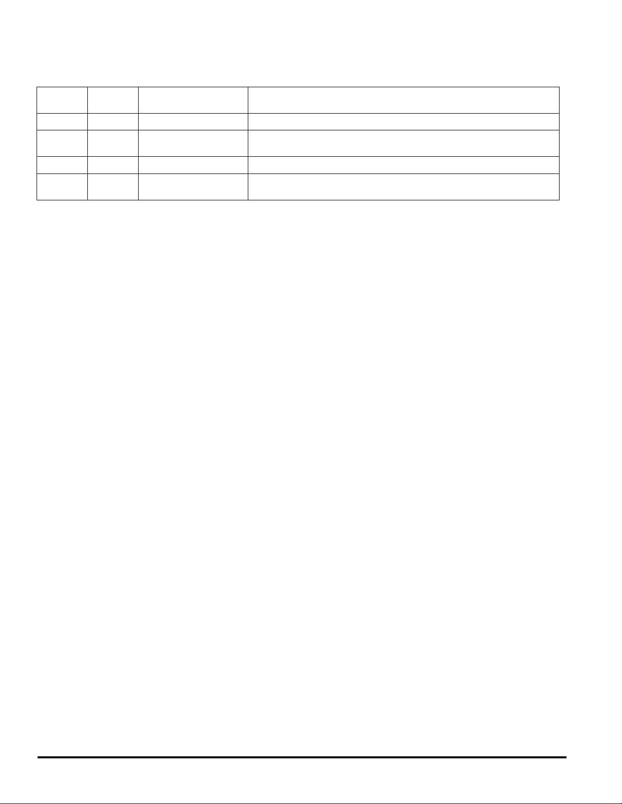
TERMINAL FUNCTION DESCRIPTION (continued)
Terminal
Name
DD
Formal Name Definition
Transistor Output
Logic Supply
Supply
nc...
I
Terminal
33 GND Ground
34 LX DC/ DC Converter Switching
35 V
36 VG Gate-Driver Circuit Power
Control circuit ground terminal for DC/DC circuit ground.
Open-drain output of the internal DC/DC converter circuit.
Control circuit power supply terminal.
Input terminal for the gate-drive voltage.
cale Semiconductor,
Frees
17550 MOTOROLA ANALOG INTEGRATED CIRCUIT DEVICE DATA
4
For More Information On This Product,
Go to: www.freescale.com
Page 5
Freescale Semiconductor, Inc.
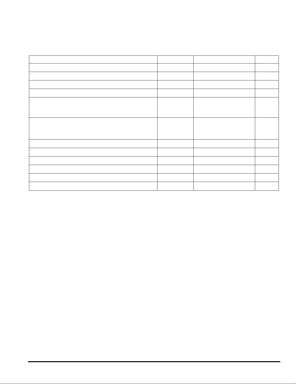
MAXIMUM RATINGS
All voltages are with respect to ground unless otherwise noted. Exceeding the ratings may cause a malfunction or permanent
damage to the device.
Rating Symbol Value Unit
Motor Supply Voltage
Gate-Driver Circuit Power Supply Voltage V
Logic Supply Voltage
Signal Input Voltage (Note 1)
Driver Output Current
Continuous (Note 2)
Peak (Note 3)
ESD Voltage
Human Body Model (Note 4)
nc...
I
cale Semiconductor,
Machine Model (Note 5)
Storage Temperature Range
Operating Ambient Temperature
Operating Junction Temperature
Thermal Resistance (Note 6) R
Power Dissipation (Note 7)
Soldering Temperature (Note 8) T
Notes
1. V
is the voltage level applied to any input terminal.
IN
is measured as the load current flowing through the H-bridge.
2. I
O
= 25°C, pulse width < 10 ms at intervals > 0.2 seconds.
3. T
A
4. ESD1 testing is performed in accordance with the Human Body Model (C
5. ESD2 testing is performed in accordance with the Machine Model (CZAP = 200 pF, RZAP = 0 Ω).
6. Mounted on 37 x 50 Cu area (1.6 mm FR-4 PCB).
7. Maximum at T
8. Soldering temperature limit is for 10 seconds maximum duration. Not designed for immersion soldering. Exceeding these limits may cause
malfunction or permanent damage to the device.
= 25°C.
A
V
M
G
V
DD
V
IN
I
O
I
OPK
V
ESD1
V
ESD2
T
STG
T
A
T
J
JA
θ
P
D
SOLDER
= 100 pF, R
ZAP
= 1500 Ω).
ZAP
-0.5 to 9.0 V
VDD-0.5 to 14 V
-0.5 to 6.0 V
-0.5 to VDD+0.5 V
0.7
2.0
±2000
±100
-65 to 150 °C
-10 to 60 °C
-10 to 150 °C
TBD °C/W
1500 mW
260 °C
A
V
Frees
MOTOROLA ANALOG INTEGRATED CIRCUIT DEVICE DATA 17550
For More Information On This Product,
Go to: www.freescale.com
5
Page 6
Freescale Semiconductor, Inc.
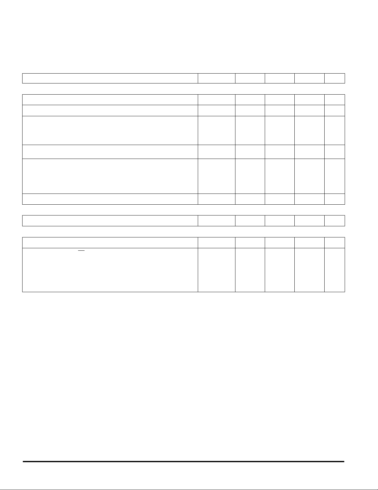
STATIC ELECTRICAL CHARACTERISTICS
Characteristics noted under conditions TA = 25°C, VDD = 3.0 V, VM = 2.5 V, GND = 0 V, f
values noted reflect the approximate parameter means at T
Characteristic Symbol Min Typ Max Unit
POWER
Motor Supply Voltage
Logic Supply Voltage
Standby Power Supply Current (Note 9)
Motor Supply Standby Current
Logic Supply Standby Current
Logic Supply Current
Gate Driver Circuit Power Supply Current (Note 10)
Standby (PSB = “L”)
nc...
I
No Signal Operating
Input Signal Operating (Note 11)
Driver Output ON Resistance (Note 12)
= 25°C under nominal conditions unless otherwise noted.
A
I
V
I
V
DDSTBY
I
I
I
R
DS(ON)
V
M
V
DD
MSTBY
V
DD
DDC0
DDCN
I
DDC
= 176 kHz unless otherwise noted. Typical
IN
1.6 2.5 5.5 V
2.5 3.0 5.5 V
–
–
–0.31.0mA
–
–
–
–0.71.2Ω
–
–
–
1.0
19
1.0
1.0
1.0
3.0
25
µA
µA
µA
mA
GATE DRIVE
Gate Driver Circuit Power Supply Voltage (Note 13)
CONTROL LOGIC
Logic Input Voltage (Note 14)
Logic Input (F, R, PSB,
High-Level Input Voltage
Low-Level Input Voltage
High-Level Input Current
Low-Level Input Current
Notes
9. Applies individually to each H-Bridge.
cale Semiconductor,
10. Average inductor current for DC/DC converter (connected between V
11. Full drive (input signal to all input terminals).
12. The total H-bridge ON resistance when V
13. When voltage is supplied externally without built-in DC/DC.
Frees
14. V
is the voltage level applied to any input.
IN
OE)
is 11.5 V.
G
V
G
V
IN
V
IH
V
IL
I
IH
I
IL
and LX [L = 1.0 mH, C = 2.2 µF]).
D
D
10 11.5 13 V
0–VDDV
VDDx0.7
–
–
-1.0
–
–
–
–
–
x0.3
V
DD
1.0
–
V
V
µA
µA
17550 MOTOROLA ANALOG INTEGRATED CIRCUIT DEVICE DATA
6
For More Information On This Product,
Go to: www.freescale.com
Page 7
Freescale Semiconductor, Inc.
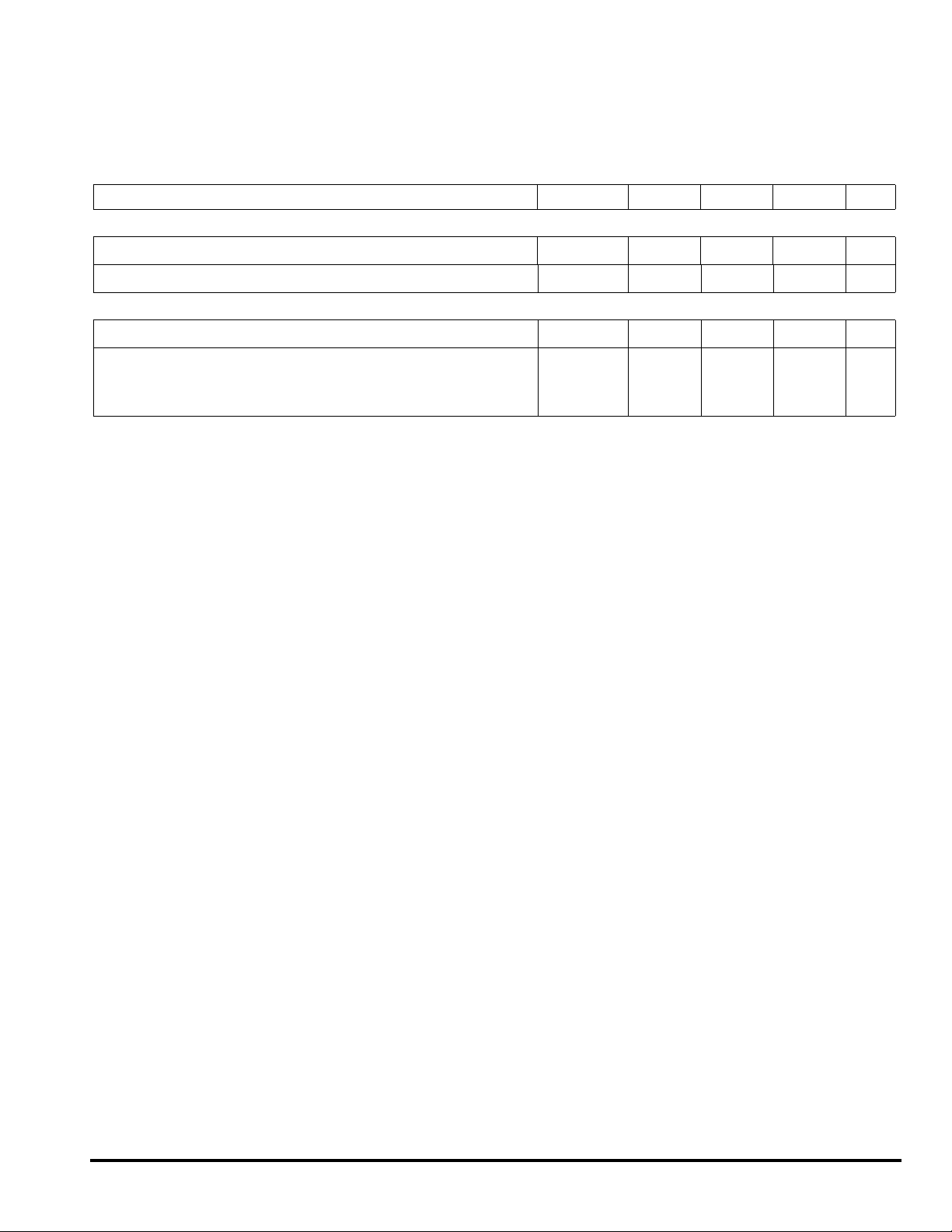
DYNAMIC ELECTRICAL CHARACTERISTICS
Characteristics noted under conditions T
Typical values noted reflect the approximate parameter means at T
Characteristic Symbol Min Typ Max Unit
INPUT
Pulse Input Frequency (Note 15)
Internal Oscillator Frequency
OUTPUT
Gate Driver Circuit Power Supply Wake-Up Time
Propagation Delay Time
Turn-ON Time
Turn-OFF Time
nc...
I
Notes
15.
f
is the signal frequency applied to an input terminal (F, R).
IN
= 25°C, VDD = 3.0 V, VM = 2.5 V, GND = 0 V, f
A
= 25°C under nominal conditions unless otherwise noted.
A
f
IN
f
OSC
t
VGON
t
PLH
t
PHL
= 176 kHz unless otherwise noted.
IN
– – 200 kHz
– 100 200 kHz
–1020ms
µs
–
–
0.2
0.2
1.0
1.0
cale Semiconductor,
Frees
MOTOROLA ANALOG INTEGRATED CIRCUIT DEVICE DATA 17550
For More Information On This Product,
Go to: www.freescale.com
7
Page 8
PSB
V
Freescale Semiconductor, Inc.
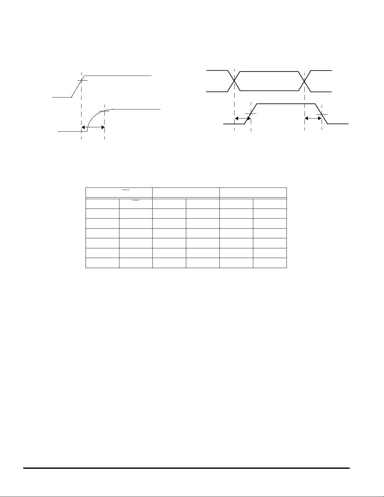
Timing Diagrams
V
t
VGON
IH
10 V
F, R ,
FO, RO
t
PLH
50%
t
50%
PHL
2.1 V
V
IL
G
Figure 2. DC/DC Converter Output Waveform
nc...
I
PSB, OE INA/ INB/ INC / IND HBA/HBB/HBC/HBC
PSB
HLLLL L
HLLHLH
HLHLHL
HLHHZ Z
HHXXZ Z
LXXXZZ
H = High.
L = Low.
Z = High impedance.
X = Don’t care.
* = A, B, C, or D.
OE
Table 1. Truth Table
IN*F IN*R HB*F HB*R
cale Semiconductor,
Figure 3. H-Bridge Output Waveform
Frees
17550 MOTOROLA ANALOG INTEGRATED CIRCUIT DEVICE DATA
8
For More Information On This Product,
Go to: www.freescale.com
Page 9

Freescale Semiconductor, Inc.
SYSTEM/APPLICATION INFORMATION
INTRODUCTION
The 17550 is a monolithic quad H-Bridge ideal for portable
electronic applications containing multiple bipolar step motors
and/or brush DC motors. The device features an on-board DC/
DC converter to provide gate-drive voltages, as well as levelshifting circuitry. The control logic translates the input signals
to the gate-driver circuitry while providing cross-conduction
suppression.
FUNCTIONAL TERMINAL DESCRIPTION
V
DD
The V
nc...
I
cale Semiconductor,
current into the logic sections of the IC. VDD has an
undervoltage threshold. If the supply voltage drops below the
undervoltage threshold, the output power stage switches to a
tri-state condition. When the supply voltage returns to a level
that is above the threshold, the power stage automatically
resumes normal operation according to the established
condition of the input terminals.
INAF, INAR, INBF, INBR, INCF, INCR, INDF, INDR
These logic input terminals control each H-Bridge output;
e.g., IN*F logic HIGH = HB*F HIGH; likewise, IN*R logic HIGH
= HB*R HIGH. However, if both “F” and “R” inputs are taken
HIGH, the associated bridge’s outputs are both tri-stated (refer
to Table 1,
OE
OE terminal is a LOW = TRUE enable input. When
OE = HIGH, all H-Bridge outputs are tri-stated (high
impedance) regardless of logic inputs states.
HBAF, HBAR, HBBF, HBBR, HBCF, HBCR, HBDF,
HBDR
terminal carries the logic supply voltage and
DD
Truth Table, page 8).
The 17550 has four operating modes: Forward, Reverse,
Brake, and Tri-Stated (High Impedance). The MOSFETs
comprising the output bridge have a total source+sink R
≤ 1.2 Ω.
The 17550 can simultaneously drive four brush DC motors
or two bipolar step motors. The drivers are designed to be
PWM’ed at frequencies up to 200 kHz.
VM
The VM terminals carry the main supply voltage and current
into the power sections of the 17550. This supply then
becomes controlled and/or modulated by the 17550 as it
delivers the power to the loads attached between the H-Bridge
output terminals. All VM terminals must be connected together
on the printed circuit board.
LX
The LX terminal is the open-drain output of the internal DC /
DC converter circuit. It is the junction for the external inductor
and the anode of the external Schottky diode.
VG
The VG terminal is the input terminal for the gate-drive
voltage. It can be supplied from the built-in DC/ DC converter
or from an external source.
Ground Terminals
All ground terminals must be tied together on the PCB.
DS(ON)
Frees
These terminals provide connection to the outputs of each
of the internal H-Bridges (see Figure 1,
Internal Block Diagram, page 2).
MOTOROLA ANALOG INTEGRATED CIRCUIT DEVICE DATA 17550
17550 Simplified
For More Information On This Product,
Go to: www.freescale.com
9
Page 10
Freescale Semiconductor, Inc.
APPLICATIONS
Introduction
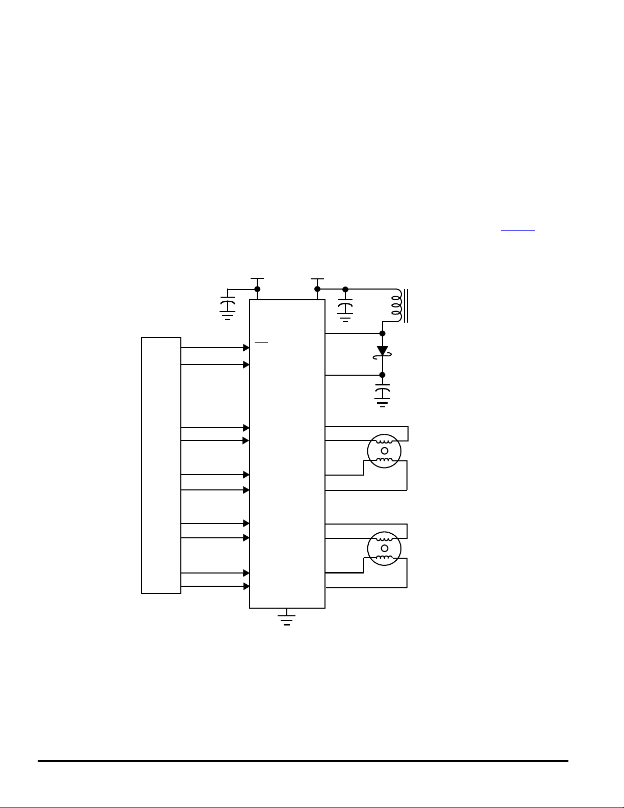
The 17550's built-in DC/DC converter must be connected to
an external inductor, rectifier, and filter capacitor. This step-up
converter generates the gate-drive voltage, V
internal gate driver circuits. Although there is some latitude in
selecting the values for the external component, care must be
taken that V
inductance will cause large instantaneous switching currents,
which may damage the device.
Important Do not use an inductance lower than 330 µH.
nc...
I
does not exceed 14 V. Additionally, too low an
G
MCU
, required by the
G
47µF
VM = 2.5 V
VM
OE
PSB
INAF
INAR
INBF
INBR
cale Semiconductor,
INCF
INCR
Frees
INDF
INDR
17550
GND
To attain high-efficiency operation, the rectifier should be a
Schottky diode, and the filter capacitor should be of the low
ESR type. Attention should be paid to proper switch mode
power supply PCB layout practice. Some experimentation may
be required to determine optimal external component values.
The recommended starting values are L = 1.0 mH, C = 2.2 µF.
The DC/DC converter includes its own internal oscillator and
does not require an external clock input.
Typical Application
A typical application schematic is shown in Figure 4.
= 3.0 V
V
DD
10
µ
V
DD
LX
VG
HBAF
HBAR
HBBF
HBBR
HBCF
HBCR
HBDF
HBDR
F
N
N
L = 1.0 mH
2.2µF
S
S
Figure 4. Typical 17550 Application
17550 MOTOROLA ANALOG INTEGRATED CIRCUIT DEVICE DATA
10
For More Information On This Product,
Go to: www.freescale.com
Page 11
Freescale Semiconductor, Inc.
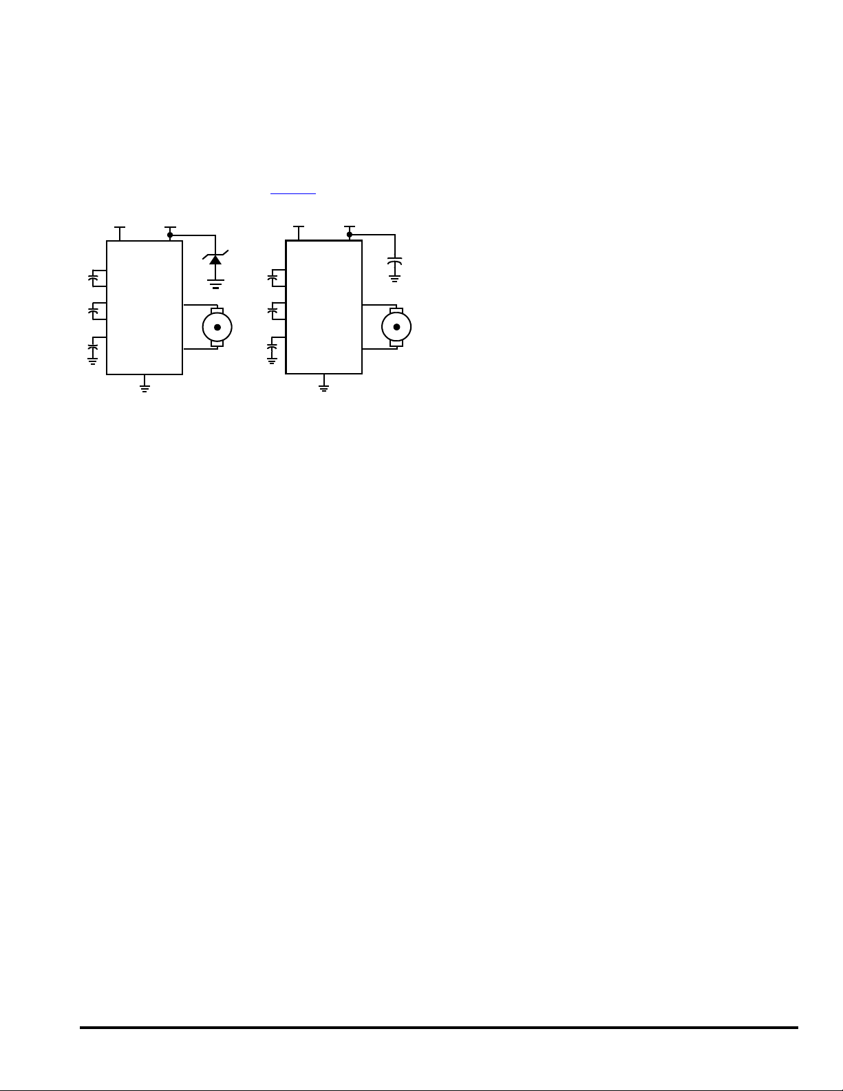
CEMF Snubbing Techniques
Care must be taken to protect the IC from potentially
damaging CEMF spikes induced when commutating currents
in inductive loads. Typical practice is to provide snubbing of
voltage transients by placing a capacitor or zener at the motor
supply voltage terminal (VM) (see Figure 5
).
5.0 V
V
DD
C1L
C1H
C2L
C2H
C
RES
nc...
I
5.0 V
175XX
VM
OUT
OUT
GND
Figure 5. CEMF Snubbing Techniques
5.0 V
V
C1L
C1H
C2L
C2H
C
cale Semiconductor,
175XX
DD
RES
GND
5.0 V
VM
OUT
OUT
Frees
MOTOROLA ANALOG INTEGRATED CIRCUIT DEVICE DATA 17550
For More Information On This Product,
Go to: www.freescale.com
11
Page 12
Freescale Semiconductor, Inc.
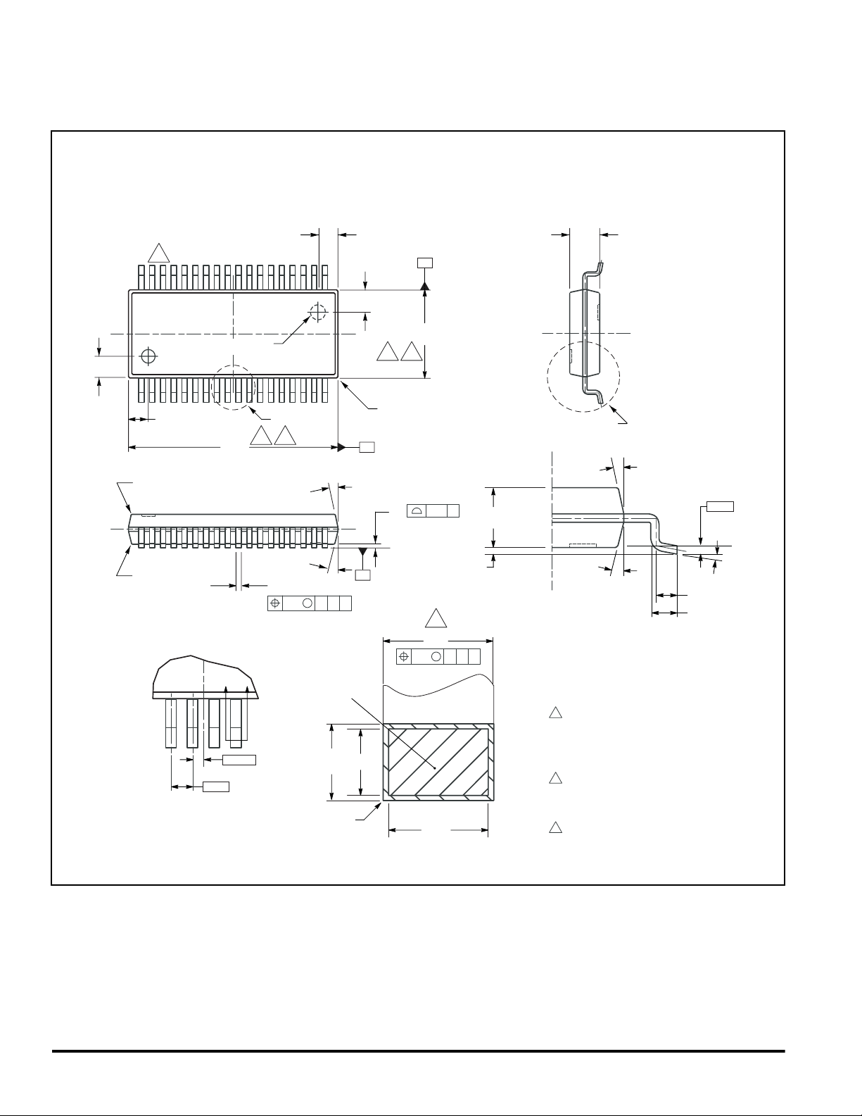
PACKAGE DIMENSIONS
EV (Pb-FREE) SUFFIX
36-LEAD VMFP
PLASTIC PACKAGE
CASE 1522-01
ISSUE O
nc...
I
cale Semiconductor,
Frees
1.20±0.10
36
1
1.30±0.10
2X
R0.15±0.10
2X
R0.15±0.10
VIEW Y
(JPN)/CAVITY #(A1)
BOTTOM SIDE
12.70
12.50
R
0.325
34X
0.65
VIEW Y
354
36X
R
19
JPN
AI
18
14˚±1˚
0.27
0.37
M
0.13 ACB
BASE METAL
0.27
0.15
PLATING
1.20±0.10
1.35±0.10
A
12˚±1˚
C
(0.20)
B
5.40
5.20
3 4
4X
R0.40±0.10
36X
SEATING PLANE
0.13 ACB
SECTION R-R
4
0.37
0.27
M
(0.30)
1.90
1.70
VIEW K
12˚±1˚
C0.10
1.90
1.70
0.20
0.00
14˚±1˚
VIEW K
VIEW ROTATED 90˚ CW
NOTES:
1.
ALL DIMENSIONS ARE IN MILLIMETERS.
2.
DIMENSIONING AND TOLERANCING PER ASME
Y14.5M, 1994.
DIMENSIONS DO NOT INCLUDE MOLD FLASH,
3.
PROTRUSIONS OR GATE BURRS. MOLD FLASH,
PROTRUSIONS OR GATE BURRS SHALL NOT
EXCEED 0.5 MM PER END. DIMENSION DOES NOT
INCLUDE INTERLEAD FLASH OR PROTRUSION.
INTERLEAD FLASH OR PROTRUSION. INTERLEAD
FLASH OR PROTRUSION SHALL NOT EXCEED
0.5 MM PER SIDE.
DIMENSIONS ARE DETERMINED AT THE OUTMOST
4.
EXTREMES OF THE PLASTIC BODY EXCLUSIVE OF
MOLD FLASH, TIE BAR BURRS, GATE BURRS AND
INTERLEAD FLASH, BUT INCLUDING ANY MISMATCH
BETWEEN THE TOP AND BOTTOM OF THE PLASTIC
BODY.
TERMINAL NUMBERS ARE SHOWN FOR REFERNCE
5.
ONLY.
0.25
GUAGE PLANE
0˚- 8˚
0.60±0.20
0.69±0.20
17550 MOTOROLA ANALOG INTEGRATED CIRCUIT DEVICE DATA
12
For More Information On This Product,
Go to: www.freescale.com
Page 13

Freescale Semiconductor, Inc.
nc...
I
NOTES
cale Semiconductor,
Frees
MOTOROLA ANALOG INTEGRATED CIRCUIT DEVICE DATA 17550
For More Information On This Product,
Go to: www.freescale.com
13
Page 14

Freescale Semiconductor, Inc.
nc...
I
NOTES
cale Semiconductor,
Frees
17550 MOTOROLA ANALOG INTEGRATED CIRCUIT DEVICE DATA
14
For More Information On This Product,
Go to: www.freescale.com
Page 15

Freescale Semiconductor, Inc.
nc...
I
NOTES
cale Semiconductor,
Frees
MOTOROLA ANALOG INTEGRATED CIRCUIT DEVICE DATA 17550
For More Information On This Product,
Go to: www.freescale.com
15
Page 16

Freescale Semiconductor, Inc.
nc...
I
cale Semiconductor,
Frees
Information in this document is provided solely to enable system and software implementers to use Motorola products. There are no express or implied
copyright licenses granted hereunder to design or fabricate any integrated circuits or integrated circuits based on the information in this document.
Motorola reserves the right to make changes without further notice to any products herein. Motorola makes no warranty, representation or guarantee
regarding the suitability of its products for any particular purpose, nor does Motorola assume any liability arising out of the application or use of any product
or circuit, and specifically disclaims any and all liability, including without limitation consequential or incidental damages. “Typical” parameters which may be
provided in Motorola data sheets and/or specifications can and do vary in different applications and actual performance may vary over time. All operating
parameters, including “Typicals” must be validated for each customer application by customer’s technical experts. Motorola does not convey any license
under its patent rights nor the rights of others. Motorola products are not designed, intended, or authorized for use as components in systems intended for
surgical implant into the body, or other applications intended to support or sustain life, or for any other application in which the failure of the Motorola product
could create a situation where personal injury or death may occur. Should Buyer purchase or use Motorola products for any such unintended or
unauthorized application, Buyer shall indemnify and hold Motorola and its officers, employees, subsidiaries, affiliates, and distributors harmless against all
claims, costs, damages, and expenses, and reasonable attorney fees arising out of, directly or indirectly, any claim of personal injury or death associated
with such unintended or unauthorized use, even if such claim alleges that Motorola was negligent regarding the design or manufacture of the part.
MOTOROLA and the Stylized M Logo are registered in the US Patent and Trademark Office. All other product or service names are the property of their
respective owners.
© Motorola, Inc. 2004
HOW TO REACH US:
USA/EUROPE/LOCATIONS NOT LISTED: JAPAN: Motorola Japan Ltd.; SPS, Technical Information Center
Motorola Literature Distribution 3-20-1 Minami-Azabu. Minato-ku, Tokyo 106-8573, Japan
P.O. Box 5405, Denver, Colorado 80217 81-3-3440-3569
1-800-521-6274 or 480-768-2130
ASIA/PACIFIC: Motorola Semiconductors H.K. Ltd.; Silicon Harbour Centre
2 Dai King Street, Tai Po Industrial Estate, Tai Po, N.T., Hong Kong
852-26668334
HOME PAGE: http://motorola.com/semiconductors
For More Information On This Product,
Go to: www.freescale.com
MPC17550
 Loading...