

Page 1

S/M No. : TCM905SEF0
Service Manual
Colour Television
CHASSIS : CM-905S/SF
Model :
DTD-
14D3/20D3/21D3 ME/MT/MP/MZ
14D4/20D4/21D4 ME/MT/MP/MZ
14D6/21D6 ME/MT/MP/MZ
14D7/20D7/21D7 ME/MT/MP/MZ
21U6/21U8 ME/MT/MP/MZ
Specification
Items Model DTD-14D3/20D3/21D3 ME/MT/MP/MZ
14D4/20D4/21D4 ME/MT/MP/MZ
14D6/21D6 ME/MT/MP/MZ
14D7/20D7/21D7 ME/MT/MP/MZ
21U6/21U8 ME/MT/MP/MZ
TV Standards PAL-SECAM-B/G,D/K,I,NTSC-M,NTSC-4.43(AV)
Mains V oltage A C 100~250V , 50/60Hz
Power Consumption Stand-by mode : 5W
Normal Operating Mode : 14”=85W, 20”=95W, 21”=105W, 21”(flat)=115W
Sound Ouput1 14/20”=5W+5W Over(80% MOD.at 1KHz THD.10%)
21U6=5W+5W Over(80% MOD.at 1KHz THD.10%)
21”,21U8=7W+7W Over(80% MOD.at 1KHz THD.10%)
Speaker 14/20”=7.5W 8 Ohm (2pcs)
21U6=5W 8 Ohm (2pcs) , 21”,21U8=12W 8 Ohm (2pcs)
Antenna 75 Ohm Unbalanced. (DIN Standard)
Tuning System FS Tuning System
Memory Channel 100 Channels
Remocon Control R-44C07
Reception Channel VHF - BAND1 : CH2-CH4
BAND2 : CH5-CH12
CABLE BAND : S1’-S3, S1-S20
HYPER BAND : S21-S41
UHF-BAND : CH21-CH69
Remark OSD
TELETEXT (Top & Flop Teletext)
PIP(AV PIP, Swap, Size, Position)
Digital Eye
DAEWOO ELECTRONICS CO., LTD
http : //svc.dwe.co.kr June.2001
Page 2

TABLE OF CONTENTS
SPECIFICATIONS .............................................................................................................. 2
SAFETY INSTRUCTION .................................................................................................... 3
CIRCUIT BLOCK DIAGRAM ............................................................................................. 4
ALIGNMENT INSTRUCTIONS .......................................................................................... 5
CM-905S/SF TYPICAL SERVICE DATA ............................................................................ 8
SCHEMATIC DIAGRAM ..................................................................................................... 11
PRINTED CIRCUIT BOARD .............................................................................................. 12
MECHANICAL EXPLODED VIEW AND PARTS LIST ...................................................... 13
ELECTRICAL PARTS LIST ............................................................................................... 19
CM-905S/SF EACH MODEL PARTS LIST ........................................................................ 29
APPENDIX (“Appendix is provided only by internet [http://svc.dwe.co.kr]”)
IC DESCRIPTION .............................................................................................................. 1
TROUBLE SHOOTING CHARTS ...................................................................................... 19
- 1 -
Page 3
SPECIFICATIONS
CAUTION
Items Model DTD-14D3/20D3/21D3 ME/MT/MP/MZ
14D4/20D4/21D4 ME/MT/MP/MZ
14D6/21D6 ME/MT/MP/MZ
14D7/20D7/21D7 ME/MT/MP/MZ
21U6/21U8 ME/MT/MP/MZ
TV Standards PAL-SECAM-B/G,D/K,I,NTSC-M,NTSC-4.43(AV)
Mains V oltage AC 100~250V , 50/60Hz
Power Consumption Stand-by mode : 5W
Normal Operating Mode :
Sound Ouput1 14/20”=5W+5W Over(80% MOD.at 1KHz THD.10%)
21U6=5W+5W Over(80% MOD.at 1KHz THD.10%)
21”,21U8=7W+7W Over(80% MOD.at 1KHz THD.10%)
Speaker 14/20”=7.5W 8 Ohm (2pcs)
21U6=5W 8 Ohm(2pcs) , 21”,21U8=12W 8 Ohm (2pcs)
Antenna 75 Ohm Unbalanced. (DIN Standard)
Tuning System FS Tuning System
Memory Channel 100 Channels
Remocon Control R-44C07
Reception Channel VHF - BAND1 : CH2-CH4
BAND2 : CH5-CH12
CABLE BAND : S1’-S3, S1-S20
HYPER BAND : S21-S41
UHF-BAND : CH21-CH69
14”=85W, 20”=95W, 21”=105W, 21”(flat)=115W
Remark OSD
TELETEXT (Top & Flop Teletext)
PIP(AV PIP, Swap, Size, Position)
Digital Eye
- 2 -
Page 4

SAFETY INSTRUCTION
CAUTION
NOTE
BEFORE SERVICING THIS CHASSIS READ THE “X-RAY RADIATION PRECAUTIONS”,
“SAFETY PRECAUTIONS” AND “PRODUCT SAFETY NOTICE” BELOW.
X-RA Y RADIATION PRECAUTIONS
1. Excessive high voltage can produce potentially hazardous X-RAY RADIATION. To avoid such hazards, the
high voltage must not exceed the specified limit. The
nominal value of the high voltage of this receiver is
25kV(21”) at max beam current. The high voltage must
not, under any circumstances, exceed 27kV(21”).
Each time a receiver requires servicing, the high voltage should be checked. It is recommended the reading
2. The only source of X-RAY RADIA TION in this TV
SAFETY PRECAUTIONS
1. Potentials of high voltage are present when this
receiver is operating. Operation of the receiver outside
the cabinet or with the back cover removed involves a
shock hazard from the receiver.
1) Servicing should not be attempted by anyone who is
not thoroughly familiar with the precautions necessary
when working on high voltage equipment.
2) Always discharge the picture tube to avoid the shock
harzard before removing the anode cap.
3) Discharge the high potential of the picture tube before
handling the tube. The picture tube is highly evacuated
and if broken, glass fragments will be violently expelled.
2. If any FUSE in this TV receiver is blown, replace it will
3. When replacing a high wattage resistor (oxide metal
4. Keep wires away from high voltage or high temperature
5. This receiver must operate between AC 100~240 volts,
of the high voltage recorded as a part of the service
recorded as a part of the service records. It is important
to use an accurate and reliable high voltage meter.
receiver is the picture tube. For continuous RADIATION
protection, the replacement tube must be exactly the
same type tube as specified in the “PA RT LIST”.
the FUSE specified in the “P ART LIST”.
film resistor) in circuit board, keep the resistor 10mm
away from circuit board.
components.
50/60Hz. NEVER connect to DC supply or any other
power or frequency.
PRODUCT SAFETY
Many electrical and mechanical parts in this chassis have
special safety-related characteristics.
These characteristics are often passed unnoticed by a
visual inspection and the X-RA Y RADIA TION protection
afforded by them cannot necessarily be obtained by using
replacement components rated for higher voltage, wattage,
etc.
Replacement parts which have these special safety characteristics are identified in this manual and its supple-
ments, electrical components having such features are
identified by designated symbol on the “P AR T LIST”.
Before replacing any of these components, read the “PA RT
LIST” in this manual carefully .
The use of substitute replacement part which do not have
the same safety characteristics as specified in the “P ART
LIST” may created X-RA Y RADIATION.
- 3 -
Page 5

CIRCUIT BLOCK DIAGRAM
CAUTION
- 4 -
Page 6

ALIGNMENT INSTRUCTIONS
CAUTION
1. AGC ADJUSTMENT
1) Pattern : P AL B/G 10CH Color BAR (RF Level = 60 dB)
2) Connect the Pattern Generator RF Output to Tuner RF Input.
3) Press the S10 Key of Service Remocon to enter the “AGC MODE”.
4) Execute the “AUTO AGC” using the V ol-Up Key.
2. SCREEN ADJUSTMENT
1) Pattern : PAL B/G Retma
2) Press the NORMAL Key to set the “NORMAL 1” mode.
3) Press the S2 Key of Service Remocon.
4) Adjust the SCREEN VOLUME on FBT so that the horizontal line reach the cut-off point.
3. FOCUS ADJUSTMENT
1) Pattern : PAL B/G Retma
2) Adjust the FOCUS VOLUME on FBT to obtain clear resolution.
4. WHITE BALANCE ADJUSTMENT
1) Press the NORMAL Key to set the “NORMAL 1” mode.
2) Press the S8 Key of Service Remocon to enter the “WHITE BALANCE” mode.
3) Adjust the each color ( R,G,B ) which appears abnormally on the screen.
5. GEOMETRIC ADJUSTMENT
1) Press the NORMAL Key to set the “NORMAL 1” mode.
2) Press the S6 Key of Service Remocon to enter the “GEOMETRIC” mode.
5-1. VERTICAL CENTER ADJUSTMENT
1) Pattern : P AL B/G Retma
2) Choose the “V-CENTER” using the Pr-Up/Down Keys.
3) Adjust the horizontal line of picture to coincide with the mechanical center marks of the CRT using the
V ol-Up/Down Keys.
If the pattern is smaller than the screen, adjust the V-size to fit.
*
5-2. VERTICAL SIZE ADJUSTMENT
1) Pattern : P AL B/G Retma
2) Choose the “V-SIZE” using the Pr-Up/Down Keys.
3) Adjust the vertical size of the picture using the Vol-Up/Down Keys.
- 5 -
Page 7

ALIGNMENT INSTRUCTIONS
5-3. HORIZONT AL CENTER ADJUSTMENT
1) Pattern : PAL B/G Retma
2) Choose the “H-CENTER” using the Pr-Up/Down Keys.
3) Adjust the vertical line of picture to coincide with the mechanical center marks of the CRT using the
Vol-Up/Down Keys.
5-4. HORIZONTAL SIZE ADJUSTMENT
1) Pattern : P AL B/G Retma
2) Choose the “H-SIZE” using the Pr-Up/Down Keys.
3) Set each side over scan to be 10% using the Vol-up/Down Keys.
5-5. PINCUSHION ADJUSTMENT
1) Pattern : P AL B/G Crosshatch
2) Choose the “PARABOLA” using the Pr-Up/Down Keys.
Adjust parabola width to fit on screen.
3) Choose the “CONER” using the Pr-Up/Down Keys.
Adjust coner parabola to fit on screen.
4) Choose the “TRAPEZIUM” using the Pr-Up/Down Keys,
Adjust trapezium to fit on screen.
5-6. S-CORRECTION ADJUSTMENT
1) Pattern : P AL B/G Crosshatch
2) Choose the “S-CORRECTION” using the Pr-Up/Down Keys.
3) Adjust each distance of horizontal line to be the same using the Vol-Up/Down Keys.
5-7. SUB-BRIGHTNESS ADJUSTMENT
1) Pattern : PAL B/G Retma
2) Press the NORMAL Keys to set the “NORMAL 1” mode.
- 6 -
Page 8
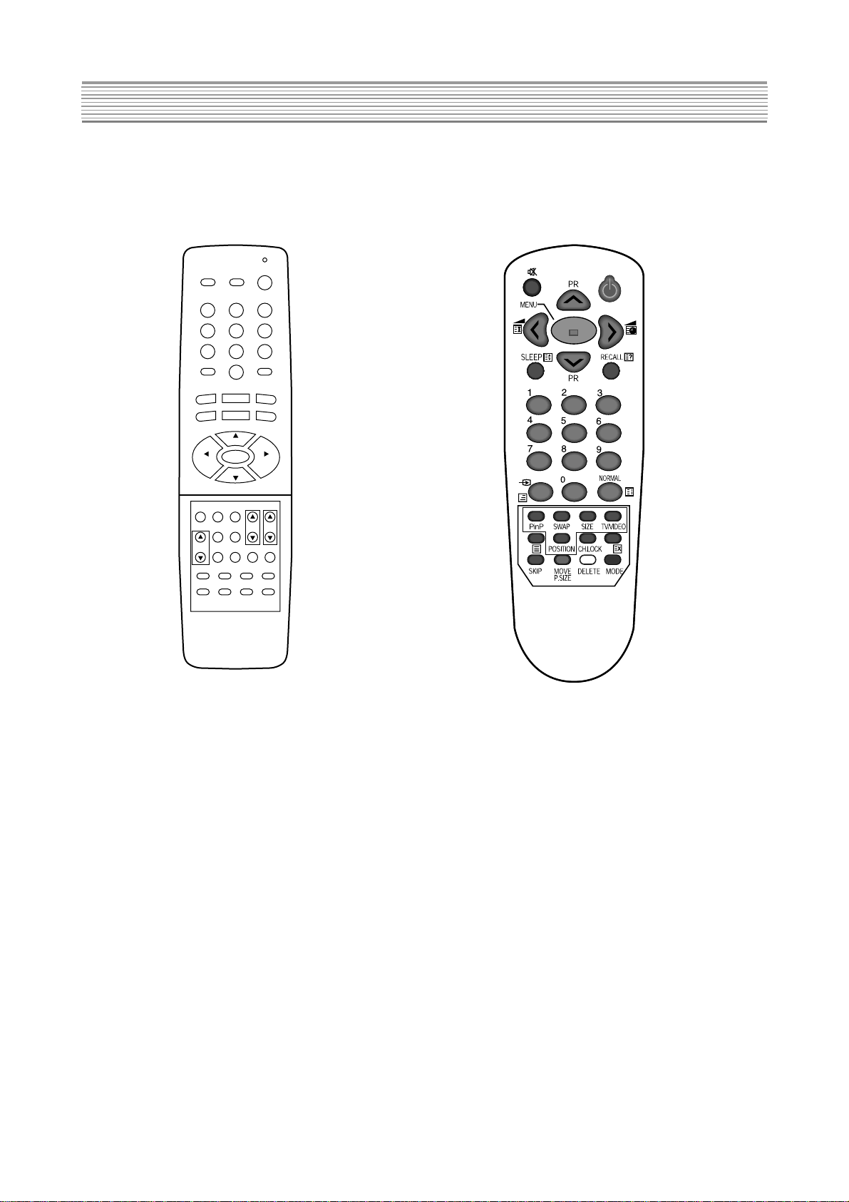
6. REMOCON
6-1. SERVICE REMOCON 6-2. USER REMOCON
ALIGNMENT INSTRUCTIONS
RECALL
S1 S2 S3
S4 S5 S6
S7 S8 S9
S10 S12
TV/CATV
SOUND MODE
PIP M/S
POSITION
TV/VIDEO
VPOSITION
3456
7
R-34SVC
POWER
MUTE
S11
TV/VIDEO
ADD/ERASE
NOISE CLEAR
SURROUND
CH
MENU
CH
PAUSE/
CH VOL
STILL
SIZE SLEEP
1
890
VOLVOL
2
6-3. SERVICE REMOCON
1) Enter SERVICE MODE : Press keys of User Remocon, as follows.
Ch91, Sharpness 0, Skip(red), Move(green), Menu.
2) Choice SERVICE MENU : Pr-Up/Down
3) Enter SERVICE SUB MENU : Vol-Up/Down
4) Adjust SERVICE MENU : Vol-Up/Down
- 7 -
Page 9
CM-905S/SF TYPICAL SERVICE DAT A
CAUTION
CM-905S/SF SVC KEY & FUNCTION DESCRIPTION
EY N NAME RFUNCTION
HEA TRUN MODE
S1
S2
S3
S4
S5
S6 PARABORA 27 48 27
S7
SCREEN
ADJUSTMENT
SOUND TEST
PICTURE TEST
NORMAL1
V-CENTER 04 04 04
V-SIZE 54 58 27
H-CENTER 11 12 14
H-SIZE 53 52 58
TRAPEZIUM 15 17 15
CORNER 05 05 05
H-EHT 03 03 03
S-CORRECTION 08 08 07
V-LINEARITY 08 07 09
V-EHT 03 03 03
PIP
R 220 220 128
G 220 220 128
B 220 220 128
PRESS THE S1 ONE TINE ----> PRESS THE S1 ANOTHER TIME
(HEATRUN MODE) (NORMAL OPRATION)
FBT SCREEN ADJUSTMENT
*
PRESS THE S2 ON TIME ----> PRESS THE S2 ANOTHER TIME
(HORIZONT AL KINE) (NORMAL OPRATION)
SOUND TEST
*
PRESS THE S3 KEY IS TOGGLE
VOLUME 00 ----> VOLUME 32 ----> VOLUME 63--->
BALANS LEFT ----> BALANS RIGHT ----> BALANS 00 ----> RELEAS
PICTURE TEST
*
PRESS THE S4 KEY IS TOGGLE
CONTRAST 00 ----> CONTRASR 32 ----> CONTRAST 63 ---->
RRIGHT 00 ----> BRIGHT 32 ----> BRIGHT 63 ---->
COLOR 00 ----> COLOR 32 ----> COLOR 63 ----> RELEASE
ADJUST NORMAL1 DA T A INITIAL DA TA
*
CONTRAST 48 63
RRIGHT 38 23
COLOR 38 32
SHARPNESS 28 32
ADJUST GEOMETRY DA T A
*
21 inch Normal 21 inch Flat Normal INITIAL DAT A(50Hz)
ADJUST PIP DA TA
*
21 inch Normal 21 inch Flat Normal
ON/OFF
ON/OFF
Line Production
Line Production
INITIAL DAT A
- 8 -
Page 10
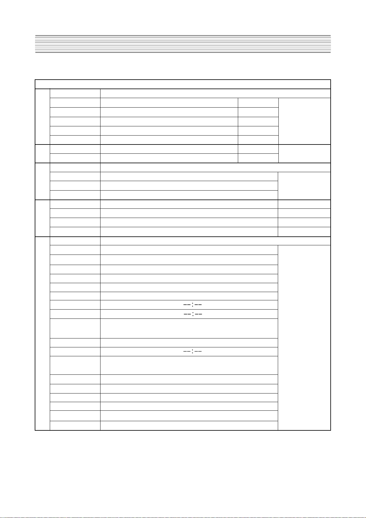
CM-905S/SF TYPICAL SERVICE DA TA
CM-905S/SF SVC KEY & FUNCTION DESCRIPTION
WHITE BALANCE
RB R LOW BEAM 127
S8
S9
S10
S11
POWER-ON-ST ART ON/OFF ON
S12
GB G LOW BEAM 146
BB B LOW BEAM 125
GG G HIGH BEAM 52
BG B HIGH BEAM 52
SUB-BRIGHT ADJUST BRIGHTNESS DA T A 35
SUB-CONTRAST ADJUST SUB CONTRAST DA T A 15
AGC TUNER AGC VOL T AGE 3.5Vdc
AUTO-AGC
DAT A 32
TEXT ARABIC/CYRILLIC/IRANIAN/EAST-LATIN//WEST-LATIN ARABIC
DIGIT AL EYE ON/OFF O N
PICTURE NORMAL 1
BLUE SCREEN ON
BASS CENTER
TREBLE CENTER
BALANCE CENTER
EFFECT OFF
CLOCK
ON TIMER
ON TIMER
ON/OFF
ON PR 1
OFF TIMER
OFF TIMER
ON/OFF
LANGUAGE ENGLISH
COLOR SYSTEM PA L
SOUND SYSTEM BG
SOUND MODE MEMORY
NAME(EACH PR) ----
TV/AV1/AV2 TV
ADJUST WHITE BALANCE DATA
*
MAIN RF AGC ADJUSTMENT KEY
*
OPTION MODE ADJUSTMENT KEY INITIAL DAT A
*
OUT DAT A
*
OFF
OFF
- 9 -
Page 11

CM-905S/SF TYPICAL SERVICE DA TA
CM-905S/SF SVC KEY & FUNCTION DESCRIPTION
TV/TEXT TV
LAST PR 1
S12
VOLUME
PICTURE SIZE NORMAL ( 4:3 )
CHILD LOCK OFF
CH LOCK OFF
SUB MENU
NO NAME FUNCTION
1 PIP ON / OFF (PIP) ON/OFF display a sub-picture
2 SWAP (PIP) The main picture and sub-picture are swapped
3 SIZE (PIP) The sub-picture will be smaller . To return to be normal size, Press this button again.
4 TV / VIDEO (PIP) To select the input for the sub pictrue
5 POSITION (PIP) The display position of the sub-picture will changed
6 S2 DA TA changed
RB 128
GB 0
SCREEN BB 0
GG 64
BG 64
Brightness 32
7 DIGITAL EYE DIGIT AL DYE funtion ON/OFF
8 ZOOM Picture size changed ( 4:3 -> 16:9 -> ZOOM -> 4:3 ->
9 TEXT TEXT funtion ON/OFF
10 CH UP USING the SERVICE MODE to CH UP/DOWN
11 CH DOWN
12 RESISTER
13 RELEASE
...
. )
- 10 -
Page 12
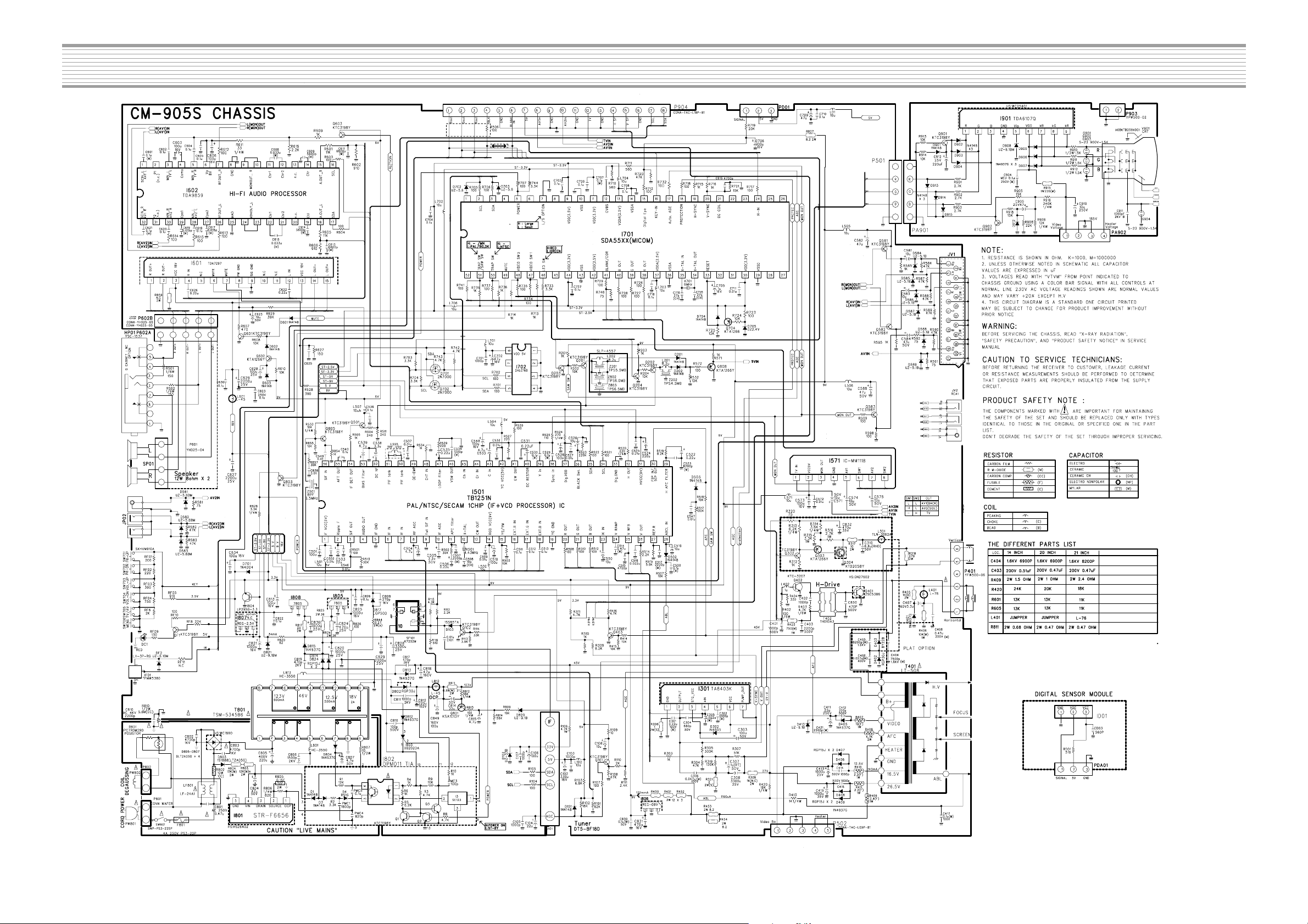
SCHEMATIC DIAGRAM
- 11 -
Page 13
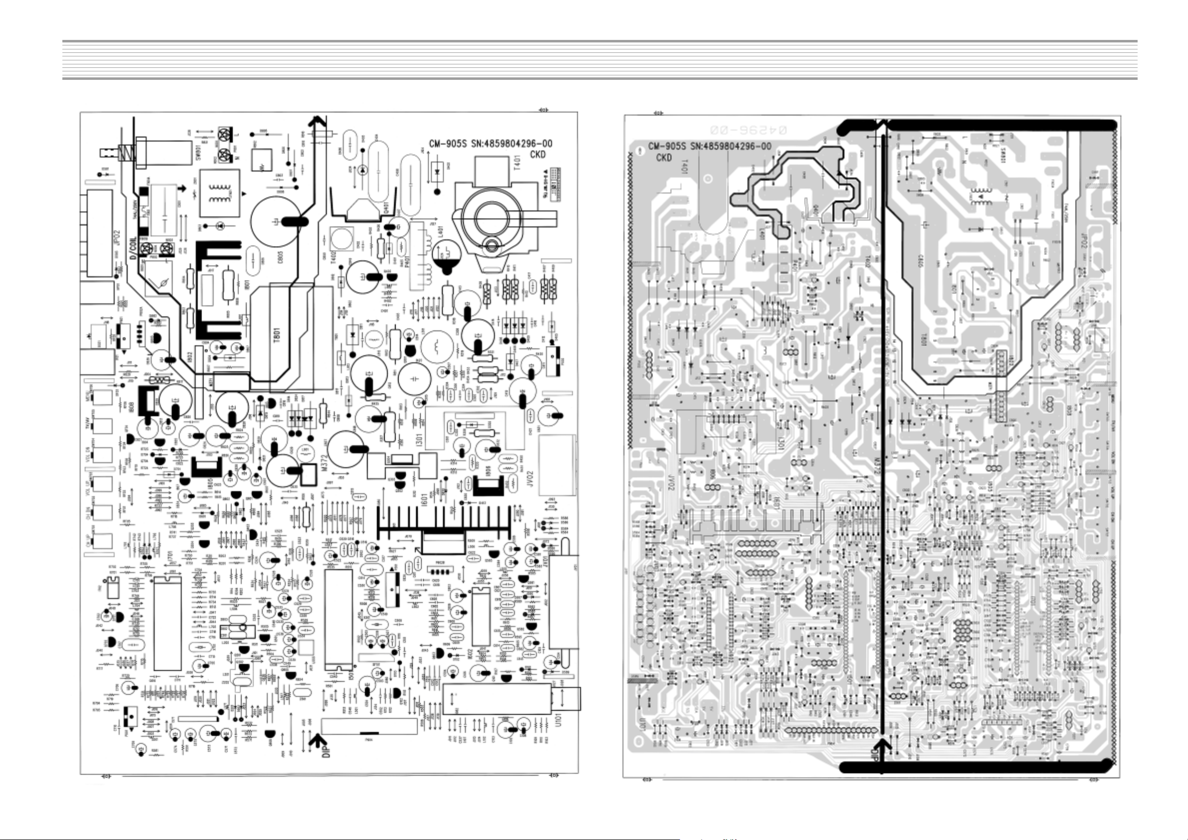
PRINTED CIRCUIT BOARD
PCB MAIN
- 12 -
Page 14
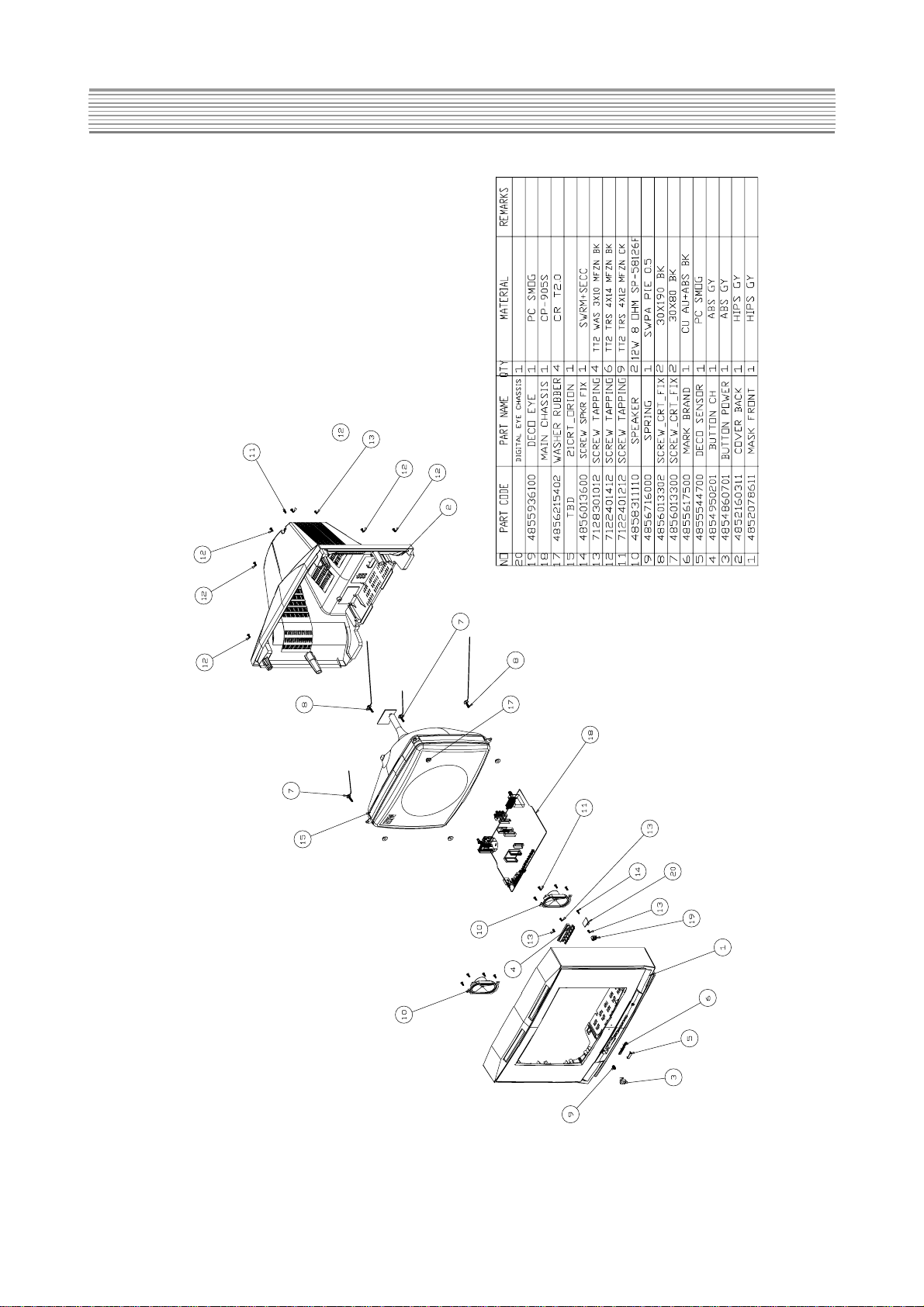
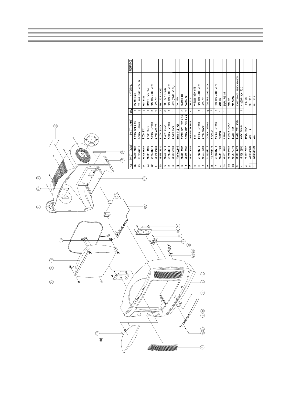
MECHANICAL EXPLODED VIEW AND PARTS LIST
CAUTION
1. DTD-21D7
- 13 -
Page 15
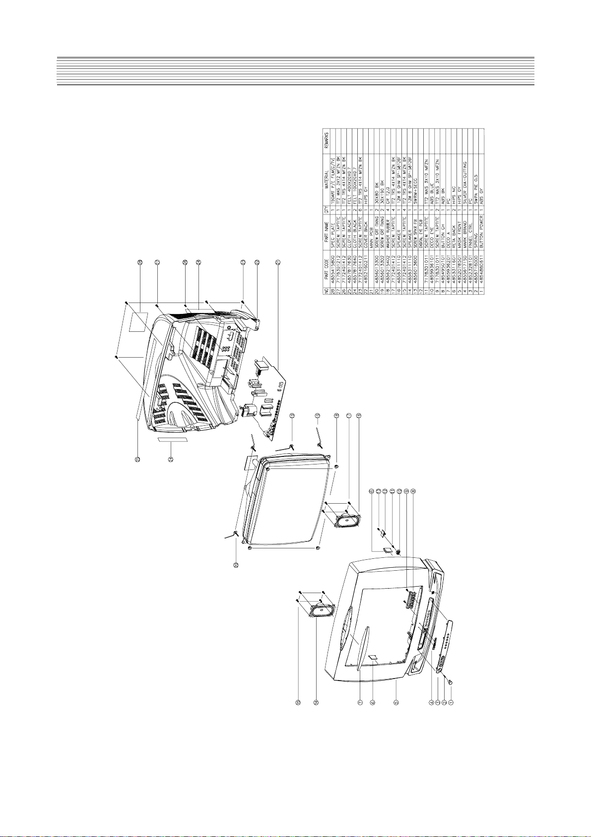
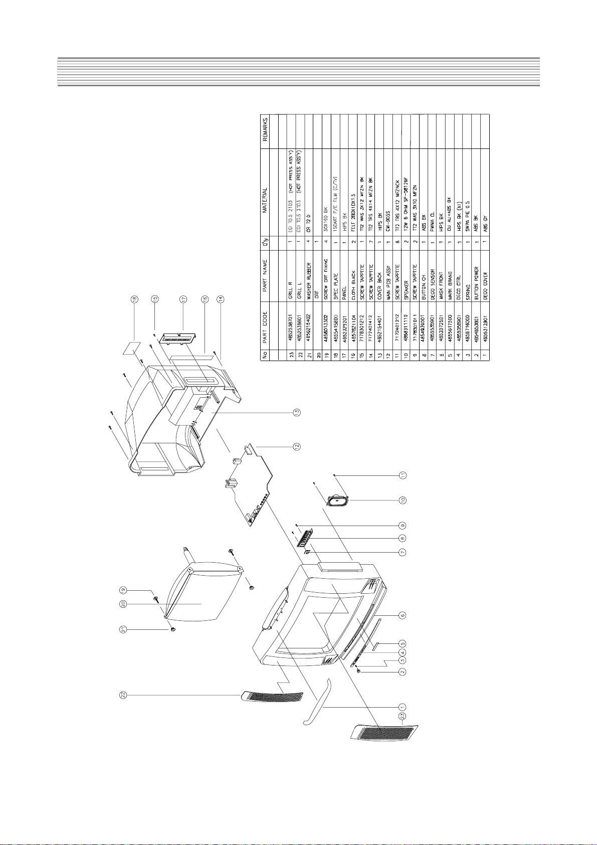
MECHANICAL EXPLODED VIEW AND PARTS LIST
2. DTD-21D6
- 14 -
Page 16
3. DTD-21D4
MECHANICAL EXPLODED VIEW AND PARTS LIST
- 15 -
Page 17
MECHANICAL EXPLODED VIEW AND PARTS LIST
4. DTD-21D3
- 16 -
Page 18

5. DTD-21U6
MECHANICAL EXPLODED VIEW AND PARTS LIST
- 17 -
Page 19

MECHANICAL EXPLODED VIEW AND PARTS LIST
6. DTD-21U8
- 18 -
Page 20

ELECTRICAL PARTS LIST
CAUTION
“ ” is safety component, so it must be used the same component.
“ ® ” is recomendable part for stock.
LOC PART CODE PART NAME DESCRIPTION REMARK
ZZ100 48B4844C07 TRANSMITTER REMOCON R-44C07 (AA)
ZZ110 PTACPWD414 ACCESSORY AS DTD-21D3MEP
100 4850Q00810 BATTERY R6P/LN
200 48586054K1 MANUAL INSTRUCTION DTM-2082CW
M001 4858213800 BAG INSTRUCTION L.D.P .E T0.05X250X400
ZZ120 PTBCSHA686 COVER BACK AS DTD-14D3ME
M211 4852152321 COVER BACK HIPS BK
M541 4855415800 SPEC PLATE 150ART P/E FILM (C/TV)
M781 4857817611 CLOTH BLACK FELT 200X20X0.7
M782 4857817640 CLOTH BLACK FELT 100X20X0.7
ZZ130 PTPKCPA686 PACKING AS DTD-14D3ME
10 6520010100 STAPLE PIN 18M/M J D O
20 6520010200 STAPLE PIN #3417
M801 4858054300 BOX DW-3 175X127X175
M811 4858187900 PAD EPS 14D3
M821 4858210600 BAG P.E L.D.P.E T0.03X1000X900
ZZ131 48519A4710 CRT GROUND NET 1401S-1015-1P
ZZ132 58G0000084 COIL DEGAUSSING DC-1450
ZZ140 PTCACAA686 CABINET AS DTD-14D3ME
40 2TF01612CL TAPE FILAMENT 0.15X12mmX55m
CRT1 PTRTPW A001 CRT AS PAL 14' ITC CRT AS
V01 58D1000046 COIL DY ODY-M1401
V02 48A96R004- RUBBER WEDGE HMR 28 SR (|0X54)
V03 4850PM001- MAGNET CP NY-225 (MINI NECK)
V04 2TC26019BE TAPE CLOTH 19X30 BEIGE
V05 2224050026 BOND SILICON RTV 122 CARTRIDGE
V901 48A96414P1 CRT BARE A34JLL90X
M191 4851936901 BUTTON CTRL 4940301+5537001
M201A 4856013300 SCREW CRT FIXING 30X80 BK
M201B 4856215402 WASHER RUBBER CR T2.0
M201C 4856013301 SCREW CRT FIXING 30X140 YL
M211A 7172401412 SCREW TAPPTITE TT2 TRS 4X14 MFZN BK
M211B 7178301212 SCREW TAPPTITE TT2 WAS 3X12 MFZN BK
M481 4854854201 BUTTON POWER ABS BK
M481A 4856716000 SPRING SWPA PIE0.5
M561 48556136SS MARK BRAND SILVER ETCHING DIA-CUTTIN
M681 4856812001 TIE CABLE NYLON66 DA100
SP01A 7172401212 SCREW TAPPTITE TT2 TRS 4X12 MFZNCK
SP01B 7172401212 SCREW TAPPTITE TT2 TRS 4X12 MFZNCK
ZZ200 PTFMSJA686 MASK FRONT AS DTD-14D3ME
M201 4852068511 MASK FRONT HIPS BK
M251 4852535810 GRILL L SECC T0.5 14D3 L
M252 4852535910 GRILL R SECC T0.5 14D3 R
ZZ210 PTSPPWA686 SPEAKER AS DTD-14D3ME
P601A 4850704S27 CONNECTOR YH025-04+35098+ULW=400
SP01 4858310910 SPEAKER SP-5090F03
SP02 4858310910 SPEAKER SP-5090F03
LOC PART CODE P ART NAME DECSCRIPTION REMARK
ZZ290 PTMPMSA686 PCB MAIN MANUAL AS DTD-14D3ME
10 2TM18006BE TAPE MASKING 6.2X500
20 2TM10006LB TAPE MASKING 3M #232-MAP-C 6.2X2000M
C308 CEYF1E332V C ELECTRO 25V RSS 3300MF (16X31.5)
C404 CMYH3C752J C MYLAR 1.6KV BUP 7500PF J
C408 CMYE2D624J C MYLAR 200V PU 0.62MF J
C801 CL1JB3474K C LINE ACROSS AC250V 0.47MF U/C/SNDF/SV
C805 CEYN2G181P C ELECTRO 400V LHS 180MF (25X35)
C806 CBYB3D152K C CERA SEMI 2KV BL(N) 1500PF K
C810 CH1AFE222M C CERA AC 4KV 2200PF M KX DE1210
C812 CEYF2C221V C ELECTRO 160V RSS 220MF (18X35.5)
C828 CEYF1E332V C ELECTRO 25V RSS 3300MF (16X31.5)
D802 DRGP30J--- DIODE RGP30J
D817 DEGP50D--- DIODE EGP50D (T APPING)
DC01 DKLR114L-- LED KLR114L
F801 5F3GB4022L FUSE GLASS TUBE V/S TL 4A 250V MF51
HP01 4859102130 JACK EARPHONE YSC-1537
I301 PTB2SW7903 HEAT SINK ASS`Y 1T A8403K-- + 7174301011
1 1TA8403K-- IC TA8403K
0000A 4857027903 HEAT SINK AL EX BK
0000B 7174301011 SCREW TAPPTITE TT2 RND 3X10 MFZN
I501 1TB1251N-- IC TB1251N
I571 1MM1118--- IC A/V SWITCH MM1118
I601 PTA2SW8218 HEAT SINK ASS`Y 1TDA7297-- + 7174301011
1 1TDA7297-- IC AUDIO AMP TDA7297
0000A 4857028218 HEAT SINK AL EX
0000B 7174301011 SCREW TAPPTITE TT2 RND 3X10 MFZN
I602 1TDA9859-- IC AUDIO PROCESSOR TDA9859
I701 1DW5555AB1 IC MICOM DW5555-AB1 ®
I702 124LC16B1B IC MEMORY 24LC16B1B
I801 PTD2SW7910 HEAT SINK ASS`Y 1STRF6656- + 7174301211
1 1STRF6656- IC POWER STR-F6656
0000A 4857027910 HEAT SINK AL EX
0000B 7174301211 SCREW TAPPTITE TT2 RND 3X12 MFZN
I802 4850M05210 MODULE POWER DPM123TIA
I803 TX0202DA-- THYRISTOR X0202DA1BA2
I804 1LP295033- IC REGULATOR LP2950 3.3V
I805 PTH2SW6900 HEAT SINK ASS`Y 1KA7805--- + 7174301011
1 1KA7805--- IC REGULATOR KA7805
0000A 4857026900 HEAT SINK AL EX
0000B 7174300811 SCREW TAPPTITE TT2 RND 3X8 MFZN
I806 PTH2SW6902 HEAT SINK ASS`Y 1K1A7809P1 + 7174301011
1 1K1A7809P1 IC REGULA TOR K1A7809API
0000A 4857026902 HEAT SINK AL EX BK
0000B 7174301011 SCREW TAPPTITE TT2 RND 3X10 MFZN
I808 PTH2SW6900 HEAT SINK ASS`Y 1KA7805--- + 7174301011
1 1KA7805--- IC REGULATOR KA7805
- 19 -
Page 21

ELECTRICAL PARTS LIST
LOC P ART CODE PART NAME DESCRIPTION REMARK
0000A 4857026900 HEAT SINK AL EX
0000B 7174300811 SCREW TAPPTITE TT2 RND 3X8 MFZN
IF01 1TS0P1238W IC PREAMP TS0P1238WI1
JP02 4859108450 JACK PIN BOARD YSC03P-4120-14A
JV01 4859200401 SOCKET RGB YRS21-R1
JV02 4859107050 JACK PIN BOARD PH-JB-9601 (PH06P-4120-C)
L555 58N0000045 COIL VCO TRF-V011
LF801 5PLF20A1-- FILTER LINE LF-20A1
M371 4853747800 RETA PCB NYLON 66
M372 4853747800 RETA PCB NYLON 66
M373 4853530901 HOLDER LED P.P
M683 4856812001 TIE CABLE NYLON66 DA100
P401 4859240120 CONN WAFER YFW500-06
P602A 4850705N18 CONNECTOR BIC-05T-25T+ULW=400
P904 4859281320 CONN WAFER TAC-L18X-A1
PW801 4859908110 CORD POWER AS 1-L0+H03VVH2-F+HOU=2200
Q401 PTH2SW7200 HEAT SINK ASS`Y TKSC5386-- + 7174301011
1 TKSC5386-- TR KSC5386
0000A 4857027200 HEAT SINK AL T1.0
0000B 7174301011 SCREW TAPPTITE TT2 RND 3X10 MFZN
R801 DEC140M290 POSISTOR ECPCC140M290
R802 RX10T109KS R CEMENT 10W 1 OHM K TRIPOD SMALL
SF101 5PK7252M-- FILTER SAW K7252M
SW801 5S40101143 SW POWER PUSH PS3-22SP (P.C.B)
T401 50H0000209 FBT LTC-508
T402 50D10A3--- TRANS DRIVE TD-10A3
T801 50M5345B6- TRANS SMPS TSM-5345B6
U101 4859721530 TUNER VARACTOR DT5-BF18D N ®
X701 5XE6R0000C CRYSTAL QUARTZ HC-49/U 6.000MHZ 20PPM
Z201 5PYXT5R5MB FILTER CERA XT 5.5MB
Z202 5PYXT4R5MB FILTER CERA XT 4.5MB
Z501 5PXLT6R5MH FILTER CERA LT 6.5MH
Z802 5PYXT6R0MB FILTER CERA XT 6.0MB
Z803 5PYXT6R5MB FILTER CERA XT 6.5MB
ZZ200 PTMPJ0A686 PCB MAIN (RHU) AS DTD-14D3ME
C411 CEXF2E220V C ELECTRO 250V RSS 22MF (13X20) TP
C413 CEXF1E102V C ELECTRO 25V RSS 1000MF (13X20) TP
C415 CEXF1V102V C ELECTRO 35V RSS 1000MF (13X25) TP
C629 CEXF1E222V C ELECTRO 25V RSS 2200MF (16X25) TP
C808 CCXB3D271K C CERA 2KV B 270PF K (T)
C811 CCXB3D102K C CERA 2KV B 1000PF K (TAPPING)
C817 CBXB3D471K C CERA SEMI 2KV BL(N) 470PF K (T)
C818 CEXF2C470V C ELECTRO 160V RSS 47MF (13X25) TP
C819 CBXB3D471K C CERA SEMI 2KV BL(N) 470PF K (T)
C820 CEXF1E102V C ELECTRO 25V RSS 1000MF (13X20) TP
C821 CEXF1C102V C ELECTRO 16V RSS 1000MF (10X20) TP
C824 CEXF1E471V C ELECTRO 25V RSS 470MF (10X16) TP
LOC PART CODE P ART NAME DECSCRIPTION REMARK
C825 CEXF1C102V C ELECTRO 16V RSS 1000MF (10X20) TP
C827 CEXF1E222V C ELECTRO 25V RSS 2200MF (16X25) TP
C829 CEXF1E222V C ELECTRO 25V RSS 2200MF (16X25) TP
C831 CEXF1C471V C ELECTRO 16V RSS 470MF (10X12.5)TP
C836 CEXF1E102V C ELECTRO 25V RSS 1000MF (13X20) TP
C849 CEXF2C101V C ELECTRO 160V RSS 100MF (16X25) TP
ZZ200 PTMPJBA686 PCB MAIN M-10 AS DTD-14D3ME
E001 4856310600 EYE LET BSR T0.2 (R2.3)
E002 4856310600 EYE LET BSR T0.2 (R2.3)
E003 4856310600 EYE LET BSR T0.2 (R2.3)
E004 4856310600 EYE LET BSR T0.2 (R2.3)
E005 4856310600 EYE LET BSR T0.2 (R2.3)
E006 4856310600 EYE LET BSR T0.2 (R2.3)
E007 4856310600 EYE LET BSR T0.2 (R2.3)
E008 4856310600 EYE LET BSR T0.2 (R2.3)
E009 4856310600 EYE LET BSR T0.2 (R2.3)
E010 4856310600 EYE LET BSR T0.2 (R2.3)
E011 4856310600 EYE LET BSR T0.2 (R2.3)
E012 4856310600 EYE LET BSR T0.2 (R2.3)
E013 4856310600 EYE LET BSR T0.2 (R2.3)
E014 4856310600 EYE LET BSR T0.2 (R2.3)
E015 4856310600 EYE LET BSR T0.2 (R2.3)
E016 4856310600 EYE LET BSR T0.2 (R2.3)
E017 4856310600 EYE LET BSR T0.2 (R2.3)
E018 4856310600 EYE LET BSR T0.2 (R2.3)
E019 4856310600 EYE LET BSR T0.2 (R2.3)
E020 4856310600 EYE LET BSR T0.2 (R2.3)
E021 4856310600 EYE LET BSR T0.2 (R2.3)
E022 4856310600 EYE LET BSR T0.2 (R2.3)
E023 4856310600 EYE LET BSR T0.2 (R2.3)
E024 4856310600 EYE LET BSR T0.2 (R2.3)
E025 4856310600 EYE LET BSR T0.2 (R2.3)
E026 4856310600 EYE LET BSR T0.2 (R2.3)
E027 4856310600 EYE LET BSR T0.2 (R2.3)
E028 4856310300 EYE LET BSR T0.2 (R1.6)
E029 4856310300 EYE LET BSR T0.2 (R1.6)
E030 4856310300 EYE LET BSR T0.2 (R1.6)
E031 4856310300 EYE LET BSR T0.2 (R1.6)
E032 4856310300 EYE LET BSR T0.2 (R1.6)
E033 4856310300 EYE LET BSR T0.2 (R1.6)
E034 4856310300 EYE LET BSR T0.2 (R1.6)
E035 4856310300 EYE LET BSR T0.2 (R1.6)
E036 4856310300 EYE LET BSR T0.2 (R1.6)
E037 4856310300 EYE LET BSR T0.2 (R1.6)
E038 4856310300 EYE LET BSR T0.2 (R1.6)
E039 4856310300 EYE LET BSR T0.2 (R1.6)
E040 4856310300 EYE LET BSR T0.2 (R1.6)
- 20 -
Page 22

ELECTRICAL PARTS LIST
LOC PART CODE PART NAME DESCRIPTION REMARK
E041 4856310300 EYE LET BSR T0.2 (R1.6)
E042 4856310300 EYE LET BSR T0.2 (R1.6)
E043 4856310300 EYE LET BSR T0.2 (R1.6)
E045 4856310300 EYE LET BSR T0.2 (R1.6)
E046 4856310300 EYE LET BSR T0.2 (R1.6)
E048 4856310300 EYE LET BSR T0.2 (R1.6)
E049 4856310300 EYE LET BSR T0.2 (R1.6)
E050 4856310300 EYE LET BSR T0.2 (R1.6)
E051 4856310300 EYE LET BSR T0.2 (R1.6)
E052 4856310300 EYE LET BSR T0.2 (R1.6)
E053 4856310300 EYE LET BSR T0.2 (R1.6)
E054 4856310300 EYE LET BSR T0.2 (R1.6)
E055 4856310300 EYE LET BSR T0.2 (R1.6)
E056 4856310300 EYE LET BSR T0.2 (R1.6)
E057 4856310300 EYE LET BSR T0.2 (R1.6)
E059 4856310600 EYE LET BSR T0.2 (R2.3)
E060 4856310600 EYE LET BSR T0.2 (R2.3)
N001 4857417500 TERM PIN DA-IB0214(D2.3/DY PIN)
N002 4857417500 TERM PIN DA-IB0214(D2.3/DY PIN)
N003 4857417500 TERM PIN DA-IB0214(D2.3/DY PIN)
N004 4857417500 TERM PIN DA-IB0214(D2.3/DY PIN)
P501 485923192S CONN WAFER YW025-06 (STICK)
P502 485923182S CONN WAFER YW025-05 (STICK)
P601 485923172S CONN WAFER YW025-04 (STICK)
PD01 485923162S CONN WAFER YW025-03 (STICK)
R106 RS01Z472J- R M-OXIDE FILM 1W 4.7K OHM J (TAPPING)
R306 RS02Z109JS R M-OXIDE FILM 2W 1 OHM J SMALL
R318 RS02Z271J- R M-OXIDE FILM 2W 270 OHM J (TAPPING)
R321 RS02Z209JS R M-OXIDE FILM 2W 2 OHM J SMALL
R406 RS01Z103J- R M-OXIDE FILM 1W 10K OHM J (TAPPING)
R407 RS01Z100J- R M-OXIDE FILM 1W 10 OHM J (TAPPING)
R408 RS02Z472JS R M-OXIDE FILM 2W 4.7K OHM J SMALL
R409 RF01Z109J- R FUSIBLE 1W 1 OHM J (TAPPING)
R410 RF01Z229J- R FUSIBLE 1W 2.2 OHM J (TAPPING)
R411 RF01Z229J- R FUSIBLE 1W 2.2 OHM J (TAPPING)
R425 RS01Z751J- R M-OXIDE FILM 1W 750 OHM J (TAPPING)
R453 RS02Z829JS R M-OXIDE FILM 2W 8.2 OHM J SMALL (TAP)
R454 RS02Z829JS R M-OXIDE FILM 2W 8.2 OHM J SMALL (TAP)
R803 RS02Z123JS R M-OXIDE FILM 2W 12K 0HM J SMALL
R804 RS02Z153JS R M-OXIDE FILM 2W 15K OHM J SMALL
R805 RF02Z158K- R FUSIBLE 2W 0.15 OHM K (TAPPING)
R811 RF02Z688K- R FUSIBLE 2W 0.68 OHM K (TAPPING)
R817 RS02Z200JS R M-OXIDE FILM 2W 20 OHM J SMALL
R844 RS02Z278JS R M-OXIDE FILM 2W 0.27 OHM J SMALL
ZZ200 PTMPJRA686 PCB MAIN RADIAL AS DTD-14D3ME
C101 CCXF1H103Z C CERA 50V F 0.01MF Z (TAPPING)
C102 CEXF1C331V C ELECTRO 16V RSS 330MF (8X11.5) TP
LOC PART CODE P ART NAME DECSCRIPTION REMARK
C104 CEXF1H220V C ELECTRO 50V RSS 22MF (5X11) TP
C105 CCXB1H102K C CERA 50V B 1000PF K (T APPING)
C106 CEXF1H101V C ELECTRO 50V RSS 100MF (8X11.5) TP
C108 CEXF1H100V C ELECTRO 50V RSS 10MF (5X11) TP
C301 CMXM2A224J C MYLAR 100V 0.22MF J
C302 CMXM2A102J C MYLAR 100V 1000PF J (TP)
C303 CEXF1H101V C ELECTRO 50V RSS 100MF (8X11.5) TP
C304 CCXB1H681K C CERA 50V B 680PF K (T APPING)
C305 CMXM2A223J C MYLAR 100V 0.022MF J TP
C306 CMXM2A473J C MYLAR 100V 0.047MF J (TP)
C307 CEXF1H109V C ELECTRO 50V RSS 1MF (5X11) TP
C401 CCXB2H102K C CERA 500V B 1000PF K (T APPING)
C402 CCXB1H102K C CERA 50V B 1000PF K (T APPING)
C403 CCXB2H222K C CERA 500V B 2200PF K (T APPING)
C407 CEXF2C339V C ELECTRO 160V RSS 3.3MF (8X16) TP
C412 CCXB2H221K C CERA 500V B 220PF K (T APPING)
C414 CCXB2H102K C CERA 500V B 1000PF K (T APPING)
C416 CCXB2H102K C CERA 500V B 1000PF K (T APPING)
C417 CMXM2A104J C MYLAR 100V 0.1MF J (TP)
C421 CMXB1H222J C MYLAR 50V EU 2200PF J (TP)
C501 CEXF1H101V C ELECTRO 50V RSS 100MF (8X11.5) TP
C503 CEXF1H220V C ELECTRO 50V RSS 22MF (5X11) TP
C504 CEXF1H479V C ELECTRO 50V RSS 4.7MF (5X11) TP
C505 CEXF1H229V C ELECTRO 50V RSS 2.2MF (5X11) TP
C506 CEXF1H228V C ELECTRO 50V RSS 0.22MF (5X11) TP
C507 CMXB1H222J C MYLAR 50V EU 2200PF J (TP)
C508 CXCH1H100D C CERA 50V CH 10PF D (TAPPING)
C510 CEXF1H101V C ELECTRO 50V RSS 100MF (8X11.5) TP
C514 CMXL1J474J C MYLAR 63V MEU 0.47MF J
C515 CMXB1H472J C MYLAR 50V EU 4700PF J (TP)
C516 CMXM2A223J C MYLAR 100V 0.022MF J TP
C517 CMXB1H222J C MYLAR 50V EU 2200PF J (TP)
C519 CEXF1H100V C ELECTRO 50V RSS 10MF (5X11) TP
C520 CMXM2A104J C MYLAR 100V 0.1MF J (TP)
C522 CEXF1H228V C ELECTRO 50V RSS 0.22MF (5X11) TP
C523 CMXB1H822J C MYLAR 50V EU 8200PF J (TP)
C524 CEXF1E221V C ELECTRO 25V RSS 220MF (8X11.5) TP
C526 CEXF1H100V C ELECTRO 50V RSS 10MF (5X11) TP
C529 CMXM2A104J C MYLAR 100V 0.1MF J (TP)
C530 CMXM2A104J C MYLAR 100V 0.1MF J (TP)
C531 CEXF1H228V C ELECTRO 50V RSS 0.22MF (5X11) TP
C533 CEXF1H479V C ELECTRO 50V RSS 4.7MF (5X11) TP
C534 CMXM2A102J C MYLAR 100V 1000PF J (TP)
C535 CEXF1H228V C ELECTRO 50V RSS 0.22MF (5X11) TP
C536 CMXM2A104J C MYLAR 100V 0.1MF J (TP)
C538 CEXF1H339V C ELECTRO 50V RSS 3.3MF (5X11) TP
C539 CEXF1H479V C ELECTRO 50V RSS 4.7MF (5X11) TP
- 21 -
Page 23

ELECTRICAL PARTS LIST
LOC PART CODE PART NAME DESCRIPTION REMARK
C548 CEXF1C101V C ELECTRO 16V RSS 100MF (6.3X11) TP
C550 CEXF1H100V C ELECTRO 50V RSS 10MF (5X11) TP
C571 CEXF1H100V C ELECTRO 50V RSS 10MF (5X11) TP
C573 CEXF1C101V C ELECTRO 16V RSS 100MF (6.3X11) TP
C574 CEXF1H100V C ELECTRO 50V RSS 10MF (5X11) TP
C575 CEXF1H100V C ELECTRO 50V RSS 10MF (5X11) TP
C581 CEXF1H100V C ELECTRO 50V RSS 10MF (5X11) TP
C582 CEXF1E470V C ELECTRO 25V RSS 47MF (5X11) TP
C583 CEXF1H100V C ELECTRO 50V RSS 10MF (5X11) TP
C584 CEXF1E470V C ELECTRO 25V RSS 47MF (5X11) TP
C588 CEXF1E470V C ELECTRO 25V RSS 47MF (5X11) TP
C601 CMXM2A104J C MYLAR 100V 0.1MF J (TP)
C603 CEXF1C101V C ELECTRO 16V RSS 100MF (6.3X11) TP
C606 CEXF1C101V C ELECTRO 16V RSS 100MF (6.3X11) TP
C608 CMXM2A333J C MYLAR 100V 0.033MF J (TP)
C609 CMXB1H562J C MYLAR 50V EU 5600PF J (TP)
C611 CMXB1H682J C MYLAR 50V 6800PF J (TP)
C613 CMXB1H682J C MYLAR 50V 6800PF J (TP)
C614 CMXB1H562J C MYLAR 50V EU 5600PF J (TP)
C615 CMXM2A333J C MYLAR 100V 0.033MF J (TP)
C617 CMXM2A153J C MYLAR 100V 0.015MF J (TP)
C619 CMXM2A153J C MYLAR 100V 0.015MF J (TP)
C621 CMXM2A104J C MYLAR 100V 0.1MF J (TP)
C622 CMXM2A224J C MYLAR 100V 0.22MF J
C623 CEXF1H100V C ELECTRO 50V RSS 10MF (5X11) TP
C626 CMXM2A224J C MYLAR 100V 0.22MF J
C628 CEXF1E101V C ELECTRO 25V RSS 100MF (6.3X11) TP
C702 CEXF1E470V C ELECTRO 25V RSS 47MF (5X11) TP
C705 CEXF1H109V C ELECTRO 50V RSS 1MF (5X11) TP
C706 CEXF1C101V C ELECTRO 16V RSS 100MF (6.3X11) TP
C707 CMXM2A104J C MYLAR 100V 0.1MF J (TP)
C709 CEXF1E470V C ELECTRO 25V RSS 47MF (5X11) TP
C715 CXCH1H270J C CERA 50V CH 27PF J (TAPPING)
C716 CXCH1H270J C CERA 50V CH 27PF J (TAPPING)
C802 CCXF3A472Z C CERA 1KV F 4700PF Z (T)
C803 CCXF3A472Z C CERA 1KV F 4700PF Z (T)
C804 CEXF1H470V C ELECTRO 50V RSS 47MF (6.3X11) TP
C807 CEXF1H479V C ELECTRO 50V RSS 4.7MF (5X11) TP
C813 CEXF1C101V C ELECTRO 16V RSS 100MF (6.3X11) TP
C814 CEXF1H220V C ELECTRO 50V RSS 22MF (5X11) TP
C815 CEXF1H479V C ELECTRO 50V RSS 4.7MF (5X11) TP
C816 CCXB2H101K C CERA 500V B 100PF K (T APPING)
C830 CMXM2A104J C MYLAR 100V 0.1MF J (TP)
C834 CEXF1C101V C ELECTRO 16V RSS 100MF (6.3X11) TP
C850 CCXB2H471K C CERA 500V B 470PF K (T APPING)
F801A 4857415001 CLIP FUSE PFC5000-0702
F801B 4857415001 CLIP FUSE PFC5000-0702
LOC PART CODE P ART NAME DECSCRIPTION REMARK
L601 58C0000096 COIL CHOKE 610G0233(470K)
L812 58C0000096 COIL CHOKE 610G0233(470K)
Q101 TKTC3198Y- TR KTC3198Y
Q102 TKTC3198Y- TR KTC3198Y
Q201 TKTC3198Y- TR KTC3198Y
Q202 TKTC3198Y- TR KTC3198Y
Q203 TKTC3198Y- TR KTC3198Y
Q204 TKTC3198Y- TR KTC3198Y
Q402 TKTC3207-- TR KTC3207 (TP)
Q403 TKTC3198Y- TR KTC3198Y
Q501 TKTC3198Y- TR KTC3198Y
Q581 TKTC3198Y- TR KTC3198Y
Q582 TKTC3198Y- TR KTC3198Y
Q583 TKTC3198Y- TR KTC3198Y
Q601 TKTC3198Y- TR KTC3198Y
Q602 TKTA1266Y- TR KTA1266Y (TP)
Q603 TKTC3198Y- TR KTC3198Y
Q701 TH2N7000-- FET H2N7000
Q702 TH2N7000-- FET H2N7000
Q704 TKTA1266Y- TR KTA1266Y (TP)
Q801 TKSA1013Y- TR KSA1013Y (TP)
Q803 TKTC3198Y- TR KTC3198Y
Q805 TKTC3198Y- TR KTC3198Y
Q808 TKTA1266Y- TR KTA1266Y (TP)
QF01 TKTC3198Y- TR KTC3198Y
R405 RN02B102JS R METAL FILM 2W 1K OHM J SMALL
R450 RN02B120JS R METAL FILM 2W 12 OHM J SMALL
R451 RN02B120JS R METAL FILM 2W 12 OHM J SMALL
R452 RN02B120JS R METAL FILM 2W 12 OHM J SMALL
R824 RN02B360JS R METAL FILM 2W 36 OHM J SMALL
R825 RN02B360JS R METAL FILM 2W 36 OHM J SMALL
R826 RN02B101JS R METAL FILM 2W 100 OHM J SMALL
SW701 5S50101090 SW TACT THVH472GCA
SW702 5S50101090 SW TACT THVH472GCA
SW703 5S50101090 SW TACT THVH472GCA
SW704 5S50101090 SW TACT THVH472GCA
SW705 5S50101090 SW TACT THVH472GCA
SW706 5S50101090 SW TACT THVH472GCA
X501 5XEX4R436C CRYSTAL QUARTZ HC-49U 4.433619M 20PP TA
ZZ200 PTMPJAA686 PCB MAIN AXIAL AS DTD-14D3ME
A001 4859814792 PCB MAIN 330X246
C103 CCZB1H102K C CERA 50V B 1000PF K (AXIAL)
C107 CCZB1H102K C CERA 50V B 1000PF K (AXIAL)
C502 CBZP1C103M C CERA SEMI 16V Y5S 0.01MF M (AXIAL)
C511 CBZF1H104Z C CERA SEMI 50V F 0.1MF Z
C512 CBZF1H104Z C CERA SEMI 50V F 0.1MF Z
C513 CBZF1H104Z C CERA SEMI 50V F 0.1MF Z
- 22 -
Page 24

ELECTRICAL PARTS LIST
LOC PART CODE PART NAME DESCRIPTION REMARK
C525 CBZP1C103M C CERA SEMI 16V Y5S 0.01MF M (AXIAL)
C532 CBZP1C103M C CERA SEMI 16V Y5S 0.01MF M (AXIAL)
C537 CBZP1C103M C CERA SEMI 16V Y5S 0.01MF M (AXIAL)
C540 CBZF1H104Z C CERA SEMI 50V F 0.1MF Z
C546 CBZP1C103M C CERA SEMI 16V Y5S 0.01MF M (AXIAL)
C547 CBZP1C103M C CERA SEMI 16V Y5S 0.01MF M (AXIAL)
C549 CBZP1C103M C CERA SEMI 16V Y5S 0.01MF M (AXIAL)
C572 CBZP1C103M C CERA SEMI 16V Y5S 0.01MF M (AXIAL)
C602 CBZF1H104Z C CERA SEMI 50V F 0.1MF Z
C604 CBZF1H104Z C CERA SEMI 50V F 0.1MF Z
C605 CBZF1H104Z C CERA SEMI 50V F 0.1MF Z
C616 CBZR1C472M C CERA 16V Y5R 4700PF M (AXIAL)
C618 CBZF1H104Z C CERA SEMI 50V F 0.1MF Z
C620 CBZF1H104Z C CERA SEMI 50V F 0.1MF Z
C630 CBZF1H104Z C CERA SEMI 50V F 0.1MF Z
C701 CCZB1H102K C CERA 50V B 1000PF K (AXIAL)
C703 CBZF1H104Z C CERA SEMI 50V F 0.1MF Z
C704 CBZF1H104Z C CERA SEMI 50V F 0.1MF Z
C708 CBZF1H104Z C CERA SEMI 50V F 0.1MF Z
C710 CBZF1H104Z C CERA SEMI 50V F 0.1MF Z
C711 CBZP1C103M C CERA SEMI 16V Y5S 0.01MF M (AXIAL)
C718 CBZF1H104Z C CERA SEMI 50V F 0.1MF Z
C720 CBZF1H104Z C CERA SEMI 50V F 0.1MF Z
C722 CBZF1H104Z C CERA SEMI 50V F 0.1MF Z
C822 CBZF1H104Z C CERA SEMI 50V F 0.1MF Z
C826 CBZF1H104Z C CERA SEMI 50V F 0.1MF Z
C838 CBZP1C103M C CERA SEMI 16V Y5S 0.01MF M (AXIAL)
D101 D1N4148--- DIODE 1N4148 (TAPPING)
D102 DUZ33B---- DIODE ZENER UZ-33B
D103 D1N4148--- DIODE 1N4148 (TAPPING)
D201 D1N4148--- DIODE 1N4148 (TAPPING)
D202 D1N4148--- DIODE 1N4148 (TAPPING)
D302 D1N4004S-- DIODE 1N4004S
D401 D1N4937G-- DIODE 1N4937G (TAPPING)
D405 D1N4937G-- DIODE 1N4937G (TAPPING)
D406 DRGP15J--- DIODE RGP15J
D407 DRGP15J--- DIODE RGP15J
D408 DRGP15J--- DIODE RGP15J
D409 DRGP15J--- DIODE RGP15J
D413 DUZ9R1BM-- DIODE ZENER UZ-9.1BM
D502 D1N4148--- DIODE 1N4148 (TAPPING)
D503 D1N4148--- DIODE 1N4148 (TAPPING)
D581 DUZ5R6BM-- DIODE ZENER UZ-5.6BM
D582 DUZ5R6BM-- DIODE ZENER UZ-5.6BM
D583 DUZ5R6BM-- DIODE ZENER UZ-5.6BM
D584 DUZ5R1B--- DIODE ZENER UZ-5.1B
D585 DUZ5R1B--- DIODE ZENER UZ-5.1B
LOC PART CODE P ART NAME DECSCRIPTION REMARK
D586 DUZ5R1B--- DIODE ZENER UZ-5.1B
D587 DUZ5R1B--- DIODE ZENER UZ-5.1B
D588 DUZ5R1B--- DIODE ZENER UZ-5.1B
D589 DUZ5R1B--- DIODE ZENER UZ-5.1B
D601 D1N4148--- DIODE 1N4148 (TAPPING)
D602 D1N4148--- DIODE 1N4148 (TAPPING)
D603 D1N4148--- DIODE 1N4148 (TAPPING)
D701 D1N4004S-- DIODE 1N4004S
D702 DUZ5R6BM-- DIODE ZENER UZ-5.6BM
D703 DUZ5R6BM-- DIODE ZENER UZ-5.6BM
D704 D1N4148--- DIODE 1N4148 (TAPPING)
D705 DUZ2R4B--- DIODE ZENER UZ-2.4B
D803 DLT2A05G-- DIODE L T2A05G (TP)
D804 D1N4937G-- DIODE 1N4937G (TAPPING)
D805 DLT2A05G-- DIODE L T2A05G (TP)
D806 DLT2A05G-- DIODE L T2A05G (TP)
D807 DLT2A05G-- DIODE L T2A05G (TP)
D808 DLT2A05G-- DIODE L T2A05G (TP)
D812 D1N4937G-- DIODE 1N4937G (TAPPING)
D813 D1N4937G-- DIODE 1N4937G (TAPPING)
D814 DRGP15J--- DIODE RGP15J
D815 D1N4937G-- DIODE 1N4937G (TAPPING)
D820 DUZ9R1BM-- DIODE ZENER UZ-9.1BM
D821 DUZ9R1BM-- DIODE ZENER UZ-9.1BM
D824 DRGP15J--- DIODE RGP15J
DF02 DUZ5R1B--- DIODE ZENER UZ-5.1B
J002 85801065GY WIRE COPPER AWG22 1/0.65 TIN COATING
J003 85801065GY WIRE COPPER AWG22 1/0.65 TIN COATING
J004 85801065GY WIRE COPPER AWG22 1/0.65 TIN COATING
J005 85801065GY WIRE COPPER AWG22 1/0.65 TIN COATING
J006 85801065GY WIRE COPPER AWG22 1/0.65 TIN COATING
J007 85801065GY WIRE COPPER AWG22 1/0.65 TIN COATING
J008 85801065GY WIRE COPPER AWG22 1/0.65 TIN COATING
J009 85801065GY WIRE COPPER AWG22 1/0.65 TIN COATING
J010 85801065GY WIRE COPPER AWG22 1/0.65 TIN COATING
J011 85801065GY WIRE COPPER AWG22 1/0.65 TIN COATING
J012 85801065GY WIRE COPPER AWG22 1/0.65 TIN COATING
J013 85801065GY WIRE COPPER AWG22 1/0.65 TIN COATING
J014 85801065GY WIRE COPPER AWG22 1/0.65 TIN COATING
J015 85801065GY WIRE COPPER AWG22 1/0.65 TIN COATING
J016 85801065GY WIRE COPPER AWG22 1/0.65 TIN COATING
J017 85801065GY WIRE COPPER AWG22 1/0.65 TIN COATING
J019 85801065GY WIRE COPPER AWG22 1/0.65 TIN COATING
J020 85801065GY WIRE COPPER AWG22 1/0.65 TIN COATING
J021 85801065GY WIRE COPPER AWG22 1/0.65 TIN COATING
J022 85801065GY WIRE COPPER AWG22 1/0.65 TIN COATING
J023 85801065GY WIRE COPPER AWG22 1/0.65 TIN COATING
- 23 -
Page 25

ELECTRICAL PARTS LIST
LOC PART CODE PART NAME DESCRIPTION REMARK
J024 85801065GY WIRE COPPER AWG22 1/0.65 TIN COATING
J025 85801065GY WIRE COPPER AWG22 1/0.65 TIN COATING
J026 85801065GY WIRE COPPER AWG22 1/0.65 TIN COATING
J027 85801065GY WIRE COPPER AWG22 1/0.65 TIN COATING
J028 85801065GY WIRE COPPER AWG22 1/0.65 TIN COATING
J029 85801065GY WIRE COPPER AWG22 1/0.65 TIN COATING
J030 85801065GY WIRE COPPER AWG22 1/0.65 TIN COATING
J031 85801065GY WIRE COPPER AWG22 1/0.65 TIN COATING
J032 85801065GY WIRE COPPER AWG22 1/0.65 TIN COATING
J033 85801065GY WIRE COPPER AWG22 1/0.65 TIN COATING
J034 85801065GY WIRE COPPER AWG22 1/0.65 TIN COATING
J035 85801065GY WIRE COPPER AWG22 1/0.65 TIN COATING
J036 85801065GY WIRE COPPER AWG22 1/0.65 TIN COATING
J037 85801065GY WIRE COPPER AWG22 1/0.65 TIN COATING
J038 85801065GY WIRE COPPER AWG22 1/0.65 TIN COATING
J039 85801065GY WIRE COPPER AWG22 1/0.65 TIN COATING
J040 85801065GY WIRE COPPER AWG22 1/0.65 TIN COATING
J041 85801065GY WIRE COPPER AWG22 1/0.65 TIN COATING
J042 85801065GY WIRE COPPER AWG22 1/0.65 TIN COATING
J043 85801065GY WIRE COPPER AWG22 1/0.65 TIN COATING
J044 85801065GY WIRE COPPER AWG22 1/0.65 TIN COATING
J045 85801065GY WIRE COPPER AWG22 1/0.65 TIN COATING
J046 85801065GY WIRE COPPER AWG22 1/0.65 TIN COATING
J047 85801065GY WIRE COPPER AWG22 1/0.65 TIN COATING
J048 85801065GY WIRE COPPER AWG22 1/0.65 TIN COATING
J049 85801065GY WIRE COPPER AWG22 1/0.65 TIN COATING
J050 85801065GY WIRE COPPER AWG22 1/0.65 TIN COATING
J051 85801065GY WIRE COPPER AWG22 1/0.65 TIN COATING
J052 85801065GY WIRE COPPER AWG22 1/0.65 TIN COATING
J053 85801065GY WIRE COPPER AWG22 1/0.65 TIN COATING
J054 85801065GY WIRE COPPER AWG22 1/0.65 TIN COATING
J055 85801065GY WIRE COPPER AWG22 1/0.65 TIN COATING
J056 85801065GY WIRE COPPER AWG22 1/0.65 TIN COATING
J057 85801065GY WIRE COPPER AWG22 1/0.65 TIN COATING
J058 85801065GY WIRE COPPER AWG22 1/0.65 TIN COATING
J059 85801065GY WIRE COPPER AWG22 1/0.65 TIN COATING
J060 85801065GY WIRE COPPER AWG22 1/0.65 TIN COATING
J061 85801065GY WIRE COPPER AWG22 1/0.65 TIN COATING
J062 85801065GY WIRE COPPER AWG22 1/0.65 TIN COATING
J063 85801065GY WIRE COPPER AWG22 1/0.65 TIN COATING
J064 85801065GY WIRE COPPER AWG22 1/0.65 TIN COATING
J065 85801065GY WIRE COPPER AWG22 1/0.65 TIN COATING
J066 85801065GY WIRE COPPER AWG22 1/0.65 TIN COATING
J067 85801065GY WIRE COPPER AWG22 1/0.65 TIN COATING
J068 85801065GY WIRE COPPER AWG22 1/0.65 TIN COATING
J069 85801065GY WIRE COPPER AWG22 1/0.65 TIN COATING
J070 85801065GY WIRE COPPER AWG22 1/0.65 TIN COATING
LOC PART CODE P ART NAME DECSCRIPTION REMARK
J071 RD-AZ101J- R CARBON FILM 1/6 100 OHM J
J072 85801065GY WIRE COPPER AWG22 1/0.65 TIN COA TING
J073 85801065GY WIRE COPPER AWG22 1/0.65 TIN COA TING
J075 85801065GY WIRE COPPER AWG22 1/0.65 TIN COA TING
J076 85801065GY WIRE COPPER AWG22 1/0.65 TIN COA TING
J077 85801065GY WIRE COPPER AWG22 1/0.65 TIN COA TING
J078 85801065GY WIRE COPPER AWG22 1/0.65 TIN COA TING
J079 85801065GY WIRE COPPER AWG22 1/0.65 TIN COA TING
J081 85801065GY WIRE COPPER AWG22 1/0.65 TIN COA TING
J082 85801065GY WIRE COPPER AWG22 1/0.65 TIN COA TING
J083 85801065GY WIRE COPPER AWG22 1/0.65 TIN COA TING
J084 85801065GY WIRE COPPER AWG22 1/0.65 TIN COA TING
J085 85801065GY WIRE COPPER AWG22 1/0.65 TIN COA TING
J086 85801065GY WIRE COPPER AWG22 1/0.65 TIN COA TING
J087 85801065GY WIRE COPPER AWG22 1/0.65 TIN COA TING
J088 85801065GY WIRE COPPER AWG22 1/0.65 TIN COA TING
J089 85801065GY WIRE COPPER AWG22 1/0.65 TIN COA TING
J090 85801065GY WIRE COPPER AWG22 1/0.65 TIN COA TING
J091 85801065GY WIRE COPPER AWG22 1/0.65 TIN COA TING
J092 85801065GY WIRE COPPER AWG22 1/0.65 TIN COA TING
J093 85801065GY WIRE COPPER AWG22 1/0.65 TIN COA TING
J094 85801065GY WIRE COPPER AWG22 1/0.65 TIN COA TING
J095 85801065GY WIRE COPPER AWG22 1/0.65 TIN COA TING
J096 85801065GY WIRE COPPER AWG22 1/0.65 TIN COA TING
J097 85801065GY WIRE COPPER AWG22 1/0.65 TIN COA TING
J098 85801065GY WIRE COPPER AWG22 1/0.65 TIN COA TING
J099 85801065GY WIRE COPPER AWG22 1/0.65 TIN COA TING
J100 85801065GY WIRE COPPER AWG22 1/0.65 TIN COA TING
J101 85801065GY WIRE COPPER AWG22 1/0.65 TIN COA TING
J102 85801065GY WIRE COPPER AWG22 1/0.65 TIN COA TING
J103 85801065GY WIRE COPPER AWG22 1/0.65 TIN COA TING
J104 85801065GY WIRE COPPER AWG22 1/0.65 TIN COA TING
J105 85801065GY WIRE COPPER AWG22 1/0.65 TIN COA TING
J106 85801065GY WIRE COPPER AWG22 1/0.65 TIN COA TING
J107 85801065GY WIRE COPPER AWG22 1/0.65 TIN COA TING
J108 85801065GY WIRE COPPER AWG22 1/0.65 TIN COA TING
J109 85801065GY WIRE COPPER AWG22 1/0.65 TIN COA TING
J110 85801065GY WIRE COPPER AWG22 1/0.65 TIN COA TING
J111 85801065GY WIRE COPPER AWG22 1/0.65 TIN COA TING
J113 85801065GY WIRE COPPER AWG22 1/0.65 TIN COA TING
J114 85801065GY WIRE COPPER AWG22 1/0.65 TIN COA TING
J116 85801065GY WIRE COPPER AWG22 1/0.65 TIN COA TING
J117 85801065GY WIRE COPPER AWG22 1/0.65 TIN COA TING
J118 85801065GY WIRE COPPER AWG22 1/0.65 TIN COA TING
J119 85801065GY WIRE COPPER AWG22 1/0.65 TIN COA TING
J120 85801065GY WIRE COPPER AWG22 1/0.65 TIN COA TING
J121 85801065GY WIRE COPPER AWG22 1/0.65 TIN COA TING
- 24 -
Page 26

ELECTRICAL PARTS LIST
LOC PART CODE PART NAME DESCRIPTION REMARK
J122 85801065GY WIRE COPPER AWG22 1/0.65 TIN COATING
J123 85801065GY WIRE COPPER AWG22 1/0.65 TIN COATING
J124 85801065GY WIRE COPPER AWG22 1/0.65 TIN COATING
J125 85801065GY WIRE COPPER AWG22 1/0.65 TIN COATING
J127 85801065GY WIRE COPPER AWG22 1/0.65 TIN COATING
J128 85801065GY WIRE COPPER AWG22 1/0.65 TIN COATING
J129 85801065GY WIRE COPPER AWG22 1/0.65 TIN COATING
J130 85801065GY WIRE COPPER AWG22 1/0.65 TIN COATING
J131 85801065GY WIRE COPPER AWG22 1/0.65 TIN COATING
J133 85801065GY WIRE COPPER AWG22 1/0.65 TIN COATING
J134 85801065GY WIRE COPPER AWG22 1/0.65 TIN COATING
J135 85801065GY WIRE COPPER AWG22 1/0.65 TIN COATING
J136 85801065GY WIRE COPPER AWG22 1/0.65 TIN COATING
J137 85801065GY WIRE COPPER AWG22 1/0.65 TIN COATING
J138 85801065GY WIRE COPPER AWG22 1/0.65 TIN COATING
J139 85801065GY WIRE COPPER AWG22 1/0.65 TIN COATING
J140 85801065GY WIRE COPPER AWG22 1/0.65 TIN COATING
L102 5CPZ100K02 COIL PEAKING 10UH K (AXIAL 3.5MM)
L201 5CPZ829K02 COIL PEAKING 8.2UH K (AXIAL 3.5MM)
L202 5CPZ829K02 COIL PEAKING 8.2UH K (AXIAL 3.5MM)
L402 5CPZ109M02 COIL PEAKING 1UH M (AXIAL 3.5MM)
L501 5CPZ100K02 COIL PEAKING 10UH K (AXIAL 3.5MM)
L502 5CPZ100K02 COIL PEAKING 10UH K (AXIAL 3.5MM)
L504 5CPZ100K02 COIL PEAKING 10UH K (AXIAL 3.5MM)
L505 5CPZ100K02 COIL PEAKING 10UH K (AXIAL 3.5MM)
L506 5CPZ100K02 COIL PEAKING 10UH K (AXIAL 3.5MM)
L507 5CPZ100K02 COIL PEAKING 10UH K (AXIAL 3.5MM)
L571 5CPZ100K02 COIL PEAKING 10UH K (AXIAL 3.5MM)
L701 5CPZ100K02 COIL PEAKING 10UH K (AXIAL 3.5MM)
L702 5CPZ100K02 COIL PEAKING 10UH K (AXIAL 3.5MM)
L703 5CPZ100K02 COIL PEAKING 10UH K (AXIAL 3.5MM)
L704 5CPZ100K02 COIL PEAKING 10UH K (AXIAL 3.5MM)
L706 5CPZ100K02 COIL PEAKING 10UH K (AXIAL 3.5MM)
L801 5MC0000100 COIL BEAD HC-3550
L813 5MC0000100 COIL BEAD HC-3550
LD01 5CPZ100K02 COIL PEAKING 10UH K (AXIAL 3.5MM)
R101 RD-AZ823J- R CARBON FILM 1/6 82K OHM J
R102 RD-AZ183J- R CARBON FILM 1/6 18K OHM J
R103 RD-AZ682J- R CARBON FILM 1/6 6.8K OHM J
R104 RD-AZ101J- R CARBON FILM 1/6 100 OHM J
R105 RD-AZ101J- R CARBON FILM 1/6 100 OHM J
R107 RD-AZ101J- R CARBON FILM 1/6 100 OHM J
R108 RD-AZ473J- R CARBON FILM 1/6 47K OHM J
R109 RD-AZ100J- R CARBON FILM 1/6 10 OHM J
R110 RD-AZ202J- R CARBON FILM 1/6 2K OHM J
R111 RD-AZ242J- R CARBON FILM 1/6 2.4K OHM J
R112 RD-AZ222J- R CARBON FILM 1/6 2.2K OHM J
LOC PART CODE P ART NAME DECSCRIPTION REMARK
R113 RD-AZ392J- R CARBON FILM 1/6 3.9K OHM J
R114 RD-AZ333J- R CARBON FILM 1/6 33K OHM J
R115 RD-AZ432J- R CARBON FILM 1/6 4.3K OHM J
R116 RD-AZ511J- R CARBON FILM 1/6 510 OHM J
R201 RD-AZ102J- R CARBON FILM 1/6 1K OHM J
R202 RD-AZ103J- R CARBON FILM 1/6 10K OHM J
R203 RD-AZ102J- R CARBON FILM 1/6 1K OHM J
R204 RD-AZ103J- R CARBON FILM 1/6 10K OHM J
R303 RD-AZ102J- R CARBON FILM 1/6 1K OHM J
R304 RD-AZ473J- R CARBON FILM 1/6 47K OHM J
R305 RD-AZ304J- R CARBON FILM 1/6 300K OHM J
R307 RD-AZ513J- R CARBON FILM 1/6 51K OHM J
R309 RD-AZ822J- R CARBON FILM 1/6 8.2K OHM J
R310 RD-AZ102J- R CARBON FILM 1/6 1K OHM J
R311 RD-AZ472J- R CARBON FILM 1/6 4.7K OHM J
R319 RD-AZ124J- R CARBON FILM 1/6 120K OHM J
R402 RD-AZ101J- R CARBON FILM 1/6 100 OHM J
R403 RD-AZ472J- R CARBON FILM 1/6 4.7K OHM J
R404 RD-AZ331J- R CARBON FILM 1/6 330 OHM J
R413 RD-4Z102J- R CARBON FILM 1/4 1K OHM J
R414 RD-AZ103J- R CARBON FILM 1/6 10K OHM J
R415 RD-AZ103J- R CARBON FILM 1/6 10K OHM J
R416 RD-AZ472J- R CARBON FILM 1/6 4.7K OHM J
R420 RD-4Z243J- R CARBON FILM 1/4 24K OHM J
R501 RD-AZ101J- R CARBON FILM 1/6 100 OHM J
R502 RD-AZ303J- R CARBON FILM 1/6 30K OHM J
R503 RD-AZ103J- R CARBON FILM 1/6 10K OHM J
R504 RD-AZ201J- R CARBON FILM 1/6 200 OHM J
R505 RD-AZ102J- R CARBON FILM 1/6 1K OHM J
R506 RD-AZ101J- R CARBON FILM 1/6 100 OHM J
R507 RD-AZ103J- R CARBON FILM 1/6 10K OHM J
R508 RD-AZ101J- R CARBON FILM 1/6 100 OHM J
R509 RD-AZ101J- R CARBON FILM 1/6 100 OHM J
R510 RD-AZ101J- R CARBON FILM 1/6 100 OHM J
R511 RD-AZ201J- R CARBON FILM 1/6 200 OHM J
R512 RD-AZ101J- R CARBON FILM 1/6 100 OHM J
R513 RD-AZ303J- R CARBON FILM 1/6 30K OHM J
R514 RD-AZ222J- R CARBON FILM 1/6 2.2K OHM J
R515 RD-AZ562J- R CARBON FILM 1/6 5.6K OHM J
R517 RD-AZ104J- R CARBON FILM 1/6 100K OHM J
R518 RD-AZ103J- R CARBON FILM 1/6 10K OHM J
R519 RD-AZ822J- R CARBON FILM 1/6 8.2K OHM J
R520 RD-4Z221J- R CARBON FILM 1/4 220 OHM J
R521 RD-AZ101J- R CARBON FILM 1/6 100 OHM J
R522 RD-AZ101J- R CARBON FILM 1/6 100 OHM J
R523 RD-AZ224J- R CARBON FILM 1/6 220K OHM J
R524 RD-4Z271J- R CARBON FILM 1/4 270 OHM J
- 25 -
Page 27

ELECTRICAL PARTS LIST
LOC PART CODE PART NAME DESCRIPTION REMARK
R525 RD-4Z111J- R CARBON FILM 1/4 110 OHM J
R527 RD-AZ221J- R CARBON FILM 1/6 220 OHM J
R529 RD-AZ221J- R CARBON FILM 1/6 220 OHM J
R532 RD-AZ103J- R CARBON FILM 1/6 10K OHM J
R533 RD-AZ103J- R CARBON FILM 1/6 10K OHM J
R534 RD-AZ102J- R CARBON FILM 1/6 1K OHM J
R535 RD-AZ101J- R CARBON FILM 1/6 100 OHM J
R540 RD-AZ472J- R CARBON FILM 1/6 4.7K OHM J
R571 RD-AZ102J- R CARBON FILM 1/6 1K OHM J
R572 RD-AZ101J- R CARBON FILM 1/6 100 OHM J
R581 RD-AZ750J- R CARBON FILM 1/6 75 OHM J
R582 RD-AZ473J- R CARBON FILM 1/6 47K OHM J
R583 RD-AZ473J- R CARBON FILM 1/6 47K OHM J
R584 RD-AZ473J- R CARBON FILM 1/6 47K OHM J
R585 RD-AZ102J- R CARBON FILM 1/6 1K OHM J
R587 RD-AZ473J- R CARBON FILM 1/6 47K OHM J
R588 RD-AZ473J- R CARBON FILM 1/6 47K OHM J
R589 RD-AZ473J- R CARBON FILM 1/6 47K OHM J
R590 RD-AZ473J- R CARBON FILM 1/6 47K OHM J
R591 RD-AZ750J- R CARBON FILM 1/6 75 OHM J
R592 RD-AZ750J- R CARBON FILM 1/6 75 OHM J
R595 RD-AZ102J- R CARBON FILM 1/6 1K OHM J
R598 RD-AZ101J- R CARBON FILM 1/6 100 OHM J
R601 RD-AZ133J- R CARBON FILM 1/6 13K OHM J
R602 RD-AZ911J- R CARBON FILM 1/6 910 OHM J
R603 RD-AZ101J- R CARBON FILM 1/6 100 OHM J
R604 RD-AZ101J- R CARBON FILM 1/6 100 OHM J
R605 RD-AZ133J- R CARBON FILM 1/6 13K OHM J
R606 RD-AZ911J- R CARBON FILM 1/6 910 OHM J
R607 RD-AZ471J- R CARBON FILM 1/6 470 OHM J
R608 RD-AZ103J- R CARBON FILM 1/6 10K OHM J
R609 RD-AZ102J- R CARBON FILM 1/6 1K OHM J
R610 RD-AZ103J- R CARBON FILM 1/6 10K OHM J
R611 RD-AZ330J- R CARBON FILM 1/6 33 OHM J
R612 RD-AZ101J- R CARBON FILM 1/6 100 OHM J
R613 RD-AZ101J- R CARBON FILM 1/6 100 OHM J
R614 RD-AZ101J- R CARBON FILM 1/6 100 OHM J
R615 RD-AZ101J- R CARBON FILM 1/6 100 OHM J
R616 RD-AZ222J- R CARBON FILM 1/6 2.2K OHM J
R627 RD-AZ151J- R CARBON FILM 1/6 150 OHM J
R628 RD-AZ391J- R CARBON FILM 1/6 390 OHM J
R629 RD-AZ393J- R CARBON FILM 1/6 39K OHM J
R701 RD-AZ101J- R CARBON FILM 1/6 100 OHM J
R702 RD-AZ101J- R CARBON FILM 1/6 100 OHM J
R703 RD-AZ332J- R CARBON FILM 1/6 3.3K OHM J
R704 RD-AZ332J- R CARBON FILM 1/6 3.3K OHM J
R705 RD-AZ101J- R CARBON FILM 1/6 100 OHM J
LOC PART CODE P ART NAME DECSCRIPTION REMARK
R706 RD-AZ101J- R CARBON FILM 1/6 100 OHM J
R707 RD-AZ101J- R CARBON FILM 1/6 100 OHM J
R710 RD-AZ561J- R CARBON FILM 1/6 560 OHM J
R711 RD-AZ561J- R CARBON FILM 1/6 560 OHM J
R712 RD-AZ101J- R CARBON FILM 1/6 100 OHM J
R713 RD-AZ102J- R CARBON FILM 1/6 1K OHM J
R714 RD-AZ102J- R CARBON FILM 1/6 1K OHM J
R715 RD-AZ102J- R CARBON FILM 1/6 1K OHM J
R716 RD-AZ102J- R CARBON FILM 1/6 1K OHM J
R717 RD-AZ101J- R CARBON FILM 1/6 100 OHM J
R718 RD-AZ101J- R CARBON FILM 1/6 100 OHM J
R719 RD-AZ203J- R CARBON FILM 1/6 20K OHM J
R720 RD-AZ473J- R CARBON FILM 1/6 47K OHM J
R721 RD-AZ103J- R CARBON FILM 1/6 10K OHM J
R723 RD-AZ101J- R CARBON FILM 1/6 100 OHM J
R724 RD-AZ103J- R CARBON FILM 1/6 10K OHM J
R725 RD-AZ103J- R CARBON FILM 1/6 10K OHM J
R726 RD-AZ101J- R CARBON FILM 1/6 100 OHM J
R727 RD-AZ101J- R CARBON FILM 1/6 100 OHM J
R728 RD-AZ101J- R CARBON FILM 1/6 100 OHM J
R729 RD-AZ101J- R CARBON FILM 1/6 100 OHM J
R732 RD-AZ101J- R CARBON FILM 1/6 100 OHM J
R733 RD-AZ332J- R CARBON FILM 1/6 3.3K OHM J
R734 RD-AZ101J- R CARBON FILM 1/6 100 OHM J
R735 RD-AZ101J- R CARBON FILM 1/6 100 OHM J
R736 RD-AZ102J- R CARBON FILM 1/6 1K OHM J
R737 RD-AZ101J- R CARBON FILM 1/6 100 OHM J
R739 RD-AZ102J- R CARBON FILM 1/6 1K OHM J
R741 RD-AZ101J- R CARBON FILM 1/6 100 OHM J
R742 RD-AZ472J- R CARBON FILM 1/6 4.7K OHM J
R743 RD-AZ472J- R CARBON FILM 1/6 4.7K OHM J
R744 RD-AZ332J- R CARBON FILM 1/6 3.3K OHM J
R746 RD-AZ750J- R CARBON FILM 1/6 75 OHM J
R751 RD-AZ472J- R CARBON FILM 1/6 4.7K OHM J
R806 RD-4Z821J- R CARBON FILM 1/4 820 OHM J
R807 RD-2Z100J- R CARBON FILM 1/2 10 OHM J
R809 RD-AZ103J- R CARBON FILM 1/6 10K OHM J
R810 RC-2Z565J- R CARBON COMP 1/2 5.6M OHM J
R812 RD-4Z363J- R CARBON FILM 1/4 36K OHM J
R813 RD-4Z163J- R CARBON FILM 1/4 16K OHM J
R814 RD-AZ563J- R CARBON FILM 1/6 56K OHM J
R820 RD-2Z620J- R CARBON FILM 1/2 62 OHM J
R821 85801065GY WIRE COPPER AWG22 1/0.65 TIN COATING
R828 RD-4Z332J- R CARBON FILM 1/4 3.3K OHM J
R854 RD-AZ102J- R CARBON FILM 1/6 1K OHM J
R855 RD-AZ103J- R CARBON FILM 1/6 10K OHM J
R857 RD-AZ303J- R CARBON FILM 1/6 30K OHM J
- 26 -
Page 28

ELECTRICAL PARTS LIST
LOC PART CODE PART NAME DESCRIPTION REMARK
RF01 RD-AZ201J- R CARBON FILM 1/6 200 OHM J
RF02 RD-AZ221J- R CARBON FILM 1/6 220 OHM J
RF03 RD-AZ391J- R CARBON FILM 1/6 390 OHM J
RF04 RD-AZ751J- R CARBON FILM 1/6 750 OHM J
RF05 RD-AZ911J- R CARBON FILM 1/6 910 OHM J
RF06 RD-AZ202J- R CARBON FILM 1/6 2K OHM J
RF08 RD-AZ223J- R CARBON FILM 1/6 22K OHM J
RF09 RD-AZ131J- R CARBON FILM 1/6 130 OHM J
RF10 RD-AZ100J- R CARBON FILM 1/6 10 OHM J
RS01 RD-AZ151J- R CARBON FILM 1/6 150 OHM J
RS02 RD-AZ151J- R CARBON FILM 1/6 150 OHM J
ZZ400 PTPMMSD405 PCB PIP MANUAL AS DTD-29M2MEO
I P02 1LP295033- IC REGULATOR LP2950 3.3V
PP01 4859279820 CONN WAFER TAC-L18P-A1 (ANGLE)
RP01 RS02Y829JS R M-OXIDE FILM 2W 8.2 OHM J SMALL
RP02 RS02Y829JS R M-OXIDE FILM 2W 8.2 OHM J SMALL
XP01 5XE20R250E CRYSTAL QUARTZ HC-49/U 20.2500MHZ 30PPM
ZZ200 PTPMJ2D405 PCB PIP CHIP B AS DTD-29M2MEO
I P01 1SDA9488XE IC CHIP PIP SDA9488X
ZZ200 PTPMJRD405 PCB PIP RADIAL AS DTD-29M2MEO
CP01 CXCH1H100D C CERA 50V CH 10PF D (TAPPING)
CP02 CXCH1H100D C CERA 50V CH 10PF D (TAPPING)
CP05 CEXF1H100V C ELECTRO 50V RSS 10MF (5X11) TP
CP08 CEXF1E470V C ELECTRO 25V RSS 47MF (5X11) TP
CP10 CEXF1E470V C ELECTRO 25V RSS 47MF (5X11) TP
CP11 CMXM2A103J C MYLAR 100V 0.01MF J (TP)
CP12 CEXF1H100V C ELECTRO 50V RSS 10MF (5X11) TP
CP14 CEXF1H109V C ELECTRO 50V RSS 1MF (5X11) TP
CP16 CEXF1H100V C ELECTRO 50V RSS 10MF (5X11) TP
CP18 CEXF1H229V C ELECTRO 50V RSS 2.2MF (5X11) TP
CP20 CEXF1H229V C ELECTRO 50V RSS 2.2MF (5X11) TP
CP21 CMXM2A473J C MYLAR 100V 0.047MF J (TP)
CP22 CMXM2A473J C MYLAR 100V 0.047MF J (TP)
CP23 CMXM2A473J C MYLAR 100V 0.047MF J (TP)
QP01 TKTC3198Y- TR KTC3198Y
QP02 TKSA1013Y- TR KSA1013Y (TP)
QP03 TKSA1013Y- TR KSA1013Y (TP)
QP04 TKSA1013Y- TR KSA1013Y (TP)
ZZ200 PTPMJAD405 PCB PIP AXIAL AS DTD-29M2MEO
10 2TM14006LB TAPE MASKING 3M #232 6.0X2000M
20 2TM10006LB TAPE MASKING 3M #232-MAP-C 6.2X2000M
A001 4859811724 PCB PIP 88X60(246X246/6) SIB
CP06 CBZP1C103M C CERA SEMI 16V Y5S 0.01MF M (AXIAL)
CP09 CBZF1H104Z C CERA SEMI 50V F 0.1MF Z
CP13 CCZF1H103Z C CERA 50V F 0.01MF Z
CP15 CCZF1H103Z C CERA 50V F 0.01MF Z
CP17 CCZF1H103Z C CERA 50V F 0.01MF Z
LOC PART CODE P ART NAME DECSCRIPTION REMARK
CP19 CCZF1H103Z C CERA 50V F 0.01MF Z
CP24 CCZB1H820K C CERA 50V B 82PF K (AXIAL)
DP02 D1N4148--- DIODE 1N4148 (TAPPING)
DP03 D1N4148--- DIODE 1N4148 (TAPPING)
DP04 D1N4148--- DIODE 1N4148 (TAPPING)
JP01 85801065GY WIRE COPPER AWG22 1/0.65 TIN COATING
JP02 85801065GY WIRE COPPER AWG22 1/0.65 TIN COATING
JP03 85801065GY WIRE COPPER AWG22 1/0.65 TIN COATING
JP04 85801065GY WIRE COPPER AWG22 1/0.65 TIN COATING
JP05 85801065GY WIRE COPPER AWG22 1/0.65 TIN COATING
JP06 85801065GY WIRE COPPER AWG22 1/0.65 TIN COATING
JP07 85801065GY WIRE COPPER AWG22 1/0.65 TIN COATING
LP02 5CPZ100K02 COIL PEAKING 10UH K (AXIAL 3.5MM)
LP03 5CPZ100K02 COIL PEAKING 10UH K (AXIAL 3.5MM)
LP04 5CPZ100K02 COIL PEAKING 10UH K (AXIAL 3.5MM)
LP05 5CPZ100K02 COIL PEAKING 10UH K (AXIAL 3.5MM)
RP03 RD-AZ221J- R CARBON FILM 1/6 220 OHM J
RP04 RD-AZ221J- R CARBON FILM 1/6 220 OHM J
RP05 RD-AZ331J- R CARBON FILM 1/6 330 OHM J
RP06 RD-AZ273J- R CARBON FILM 1/6 27K OHM J
RP07 RD-AZ101J- R CARBON FILM 1/6 100 OHM J
RP08 RD-AZ101J- R CARBON FILM 1/6 100 OHM J
RP09 RD-AZ101J- R CARBON FILM 1/6 100 OHM J
RP10 RD-AZ151J- R CARBON FILM 1/6 150 OHM J
RP11 RD-AZ151J- R CARBON FILM 1/6 150 OHM J
RP12 RD-AZ151J- R CARBON FILM 1/6 150 OHM J
RP13 RD-AZ102J- R CARBON FILM 1/6 1K OHM J
RP14 RD-AZ102J- R CARBON FILM 1/6 1K OHM J
RP15 RD-AZ102J- R CARBON FILM 1/6 1K OHM J
ZZ600 PTCPMSA686 PCB CRT MANUAL AS DTD-14D3ME
10 2193100710 SOLDER POWER BAR S62S-PB37-SB1
20 2193011101 SOLDER WIRE RS 60-1.2 1.6A
30 2291050615 FLUX SOLDER DF-2012U
40 2291050301 FLUX SOLVENT IM-1000
50 2291140501 WAX COVER
C910 CEYF2E100V C ELECTRO 250V RSS 10MF (10X20)
C911 CCYB3D102K C CERA 2KV B 1000PF K
G901 4SG0D00103 SPARK GAP S-23 900V-1.5KV
G902 4SG0D00103 SPARK GAP S-23 900V-1.5KV
G903 4SG0D00103 SPARK GAP S-23 900V-1.5KV
G904 4SG0D00103 SPARK GAP S-23 900V-1.5KV
I901 PTC3SW1100 HEA T SINK ASS`Y 1TDA6107Q- + 7174300811
1 1TDA6107Q- IC VIDEO TDA6107Q
0000A 4857031100 HEAT SINK A1050P-H24 T2.0
0000B 7174300811 SCREW TAPPTITE TT2 RND 3X8 MFZN
P501A 4850706S12 CONNECTOR YH025-06+YST025+ULW=300
P502A 4850705S02 CONNECTOR YH025-05+YST025+ULW=200
- 27 -
Page 29

ELECTRICAL PARTS LIST
LOC PART CODE PART NAME DESCRIPTION REMARK
R915 RS01Y391J- R M-OXIDE FILM 1W 390 OHM J
SCT1 4859303430 SOCKET CRT PCS633A
ZZ200 PTCPJRA686 PCB CRT RADIAL AS DTD-14D3ME
C902 CXCH1H120J C CERA 50V CH 12PF J (TAPPING)
C904 CMXL2E104K C MYLAR 250V MEU 0.1MF K
C905 CEXF1E470V C ELECTRO 25V RSS 47MF (5X11) TP
C912 CEXF1E221V C ELECTRO 25V RSS 220MF (8X11.5) TP
Q901 TKTA1266Y- TR KTA1266Y (TP)
Q902 TKTC3198Y- TR KTC3198Y
ZZ200 PTCPJAA686 PCB CRT AXIAL AS DTD-14D3ME
10 2TM14006LB TAPE MASKING 3M #232 6.0X2000M
20 2TM10006LB TAPE MASKING 3M #232-MAP-C 6.2X2000M
A001 4859828013 PCB CRT 110X68(246X246/6) SIB
D901 D1N4148--- DIODE 1N4148 (T APPING)
D902 D1N4148--- DIODE 1N4148 (T APPING)
D903 D1N4148--- DIODE 1N4148 (T APPING)
D904 D1N4148--- DIODE 1N4148 (T APPING)
D905 D1N4937G-- DIODE 1N4937G (T APPING)
D906 D1N4937G-- DIODE 1N4937G (T APPING)
D907 D1N4937G-- DIODE 1N4937G (T APPING)
D912 D1N4148--- DIODE 1N4148 (T APPING)
D913 D1N4148--- DIODE 1N4148 (T APPING)
D914 D1N4148--- DIODE 1N4148 (T APPING)
D915 D1N4148--- DIODE 1N4148 (T APPING)
J901 85801065GY WIRE COPPER AWG22 1/0.65 TIN COATING
J903 85801065GY WIRE COPPER AWG22 1/0.65 TIN COATING
J904 85801065GY WIRE COPPER AWG22 1/0.65 TIN COATING
R901 RD-AZ272J- R CARBON FILM 1/6 2.7K OHM J
R902 RD-AZ272J- R CARBON FILM 1/6 2.7K OHM J
R903 RD-AZ272J- R CARBON FILM 1/6 2.7K OHM J
R905 RD-AZ153J- R CARBON FILM 1/6 15K OHM J
R908 RD-AZ223J- R CARBON FILM 1/6 22K OHM J
R909 RD-4Z123J- R CARBON FILM 1/4 12K OHM J
R910 RC-2Z152K- R CARBON COMP 1/2 1.5K OHM K
R911 RC-2Z152K- R CARBON COMP 1/2 1.5K OHM K
R912 RC-2Z152K- R CARBON COMP 1/2 1.5K OHM K
R913 RD-AZ103J- R CARBON FILM 1/6 10K OHM J
R914 RD-AZ152J- R CARBON FILM 1/6 1.5K OHM J
R916 RD-4Z244J- R CARBON FILM 1/4 240K OHM J
R918 RD-AZ153J- R CARBON FILM 1/6 15K OHM J
- 28 -
Page 30

- 29 -
Inch Different Part List
Loc Part_nm 14INCH 20INCH 21INCH 21INCH(Flat)
C404 C Mylar 1.6KV BUP 7500PF J 1.6KV BUP 9100PF J 1.6KV BUP 8200PF J 1.6KV BUP 9100PF J Main Manul AS
C408 C Mylar 200V PU 0.62MF J 200V PU 0.62MF J 200V PU 0.47MF J 200V PU 0.36MF J Main Manul AS
J124 Wire Copper WG22 1/0.65 TIN COATIN WG22 1/0.65 TIN COATIN 0 0 Main Axial AS
L401 oil H-Lineart 0 0 L-76(76.5UH) L-76(76.5UH) Main Manual as
P501A Connector 025-06-YST025+ULW=3 025-06+YST025+ULW=4 025-06+YST025+ULW=4 025-06+YST025+ULW=4 CRT PCB Manual AS
P502A Connector 025-05-YST025+ULW=2 025-05+YST025+ULW=3 025-05+YST025+ULW=3 025-05+YST025+ULW=3 CRT PCB Manual AS
P601A Connector H025-04+35098+ULW=40 H025-04+35098+UL W=50 H025-04+35098+ULW=50 H025-04+35098+ULW=50 SPK AS
R409 R Fusible 1W 1 1W 1.5 1W 2.4 1W 2.4 Main M-10 AS
R420 R Carbon 1/4 24K OHM J 1/4 24K OHM J 1/4 18K OHM J 1/4 13K OHM J Main Axial AS
R601 R Carbon 1/6 13K OHM J 1/6 13K OHM J 1/6 11K OHM J 1/6 13K OHM J Main Axial AS
R605 R Carbon 1/6 13K OHM J 1/6 13K OHM J 1/6 11K OHM J 1/6 13K OHM J Main Axial AS
R801 Posistro ECPCC140M290 2322 662 96709 2322 662 96709 2322 662 96709 Main Manual AS
R811 R Fusible 2W 0.68 2W 0.47 2W 0.47 2W 0.33 Main M-10 AS
SCT1 Socker CRT PCS633A PCS629-03C PCS629-03C PCS629-03C Main Manual AS
SP01 Speaker SP-5090F03 SP-5090F03 12W 8
SP02 Speaker SP-5090F03 SP-5090F03 12W 8
SP-58126F 5W 8 SP-58126F SPK AS
SP-58126F 5W 8 SP-58126F SPK AS
CAUTION
CM-905S/SF EACH MODEL PARTS LIST
Page 31

686, AHYEON-DONG MAPO-GU
SEOUL, KOREA
C.P.O. BOX 8003 SEOUL, KOREA
TELEX : DWELEC K28177-8
CABLE : “DAEWOOELEC”
E-mail :djkoo@web.dwe.co.kr
Page 32

APPENDIX
IC DESCRIPTION
TB1251CN
PAL/NTSC/SECAM 1CHIP ( IF + VCD PROCESSOR ) IC
The TB1251N is a TV signal processor IC, which contains
PIF, SIF , V ideo, Chroma and deflection signal processors
for worldwide Multi-color systems. Also, it has V and EW
geometric correction Outputs.
The line-up and flexibility of this TB1251 series contributes
to reduce development costs and components in a TV
sets.
FEATURES
IF STAGE
• Multi-system IF
• SIF 4.5 ~ 6.5 MHz
• One External BPF for Multi-SIF carrier
• Inter/Sprit carrier inputs
• V C O tank coil alignment free
• for L system,
Positive demodulation
V low Ch
AM Sound demodulation(Sprit carrier)
VIDEO ST AGE
• Built-in Y delay line (8 adjustable steps)
• Built in C trap filter (Swithable)
• VSM output
SDIP56-P-600
Weight : 5.55g (typ)
TEXT ST AGE
• Built-in AKB
AKB on/off
AKB Color temperature control
• Analog RGB interface
• ABL / ACL
DEFLECTION ST AGE
• Built-in H-VCO
• V/EW geometric corrections
• Stnd Along Sync input
• Sand Castle Pulse Output
(HD+VD+Gate Pulse)
CHROMA ST AGE
• Multi-color Demodulation
• Automatic Chroma Identification
• 1 Xtal for Multi-color Systems
(3.58MHz/4.43MHz/M-PAL/N-PAL)
• Built-in 1H Delay line
• Cb/Cr input
• Built-in BPF/TOF
• Fsc Output
• Two NTSC demodulation phase
- 1 -
Page 33

TERMINAL INTERFACE
PIN NAME FUNCTION INTERFACE
1 IF VCC A Vcc terminal for the IF circuit.
Supply 5V.
2 RIPPLE A terminal should be connected to an internal
FILTE R bias filler. Put a capacilor.
3 SIF OUT An output terminal for a 2’nd SIF signal, that
is mixed down by a regenerated carrier.
The SIF frequencies are able to convert into
only 6.5MHz, in order to eliminate SIF BPFs
to single 6.5MHz.
APPENDIX
IC DESCRIPTION
-
4 AUDIO OUT An output terminal for audio signal.
FM Det.signal, inputted to pin53, is output.
An internal audio attenator controls the output
levels.
5 IF GND The GND terminal for IF circuit.
6 IF IN Input terminals for IF signals. Pin 6 and 7 are
7 IF IN the both input poles of a differential amplifier.
The normal input level is 90dB( V )( Pin6-7),
input impedance is 1.5 k ohms.
-
- 2 -
Page 34

APPENDIX
IC DESCRIPTION
PIN NAME FUNCTION INTERFACE
8 RF AGC An output terminal for RF AGC.
A pull up resister is required because of its
open collector output. A de-coupling capacitor
is also connected to reduce noise.
9 1’st SIF IN An input terminal for 1’st SIF signal.
10 IF AGC A terminal should be connceted to an IF AGC
filter. Connect 2.2uF capacitor to Vcc.
11 APC FIL T ER A terminal should be connected with an APC
filter for chroma demodulation.
This terminal voltage controls the frequency
of VCXO.
12 X’TAL A terminal should be connected with a
(4.43MHZ) 4.433619MHz X’tal oscillator. The oscillated
signal leads to the chroma demodulation, H
out frequency tuning, AFT, etc.
- 3 -
Page 35

PIN NAME FUNCTION INTERFACE
13 CW OUT An output terminal for the continuous chroma
sub-carrier frequency wave, with an amplitude
of 0.7Vp-p (typ).
Also the dc level shows chroma killer status,
with a level of 3.5V for B/W and 1.5V for
Color.
14 RGB VCC(9V) A Vcc terminal for RGB block, PIF det. Output
and sound output circuit. Supply 9V.
15 YS/YM SW A terminal for switching of EXT RGB Mode
/Spot killer and fast Half tone.
APPENDIX
IC DESCRIPTION
16 EXT.R IN Input terminals for EXT RGB signals. The
17 EXT.G IN signals are clamped by capacitors, therefore
18 EXT.B IN the input impedance should be low, 100 ohms
or less is recommended.
For this input, the brightness and RGB
contrast is adjustable, the ABL/ACL limits the
output level. This ABL/ACL may be turned On
and OFF.
OFF : for small area like OSD
ON : for large area like TELETEXT
(input level 0.7Vp-p/100IRE)
19 Y/C GND The GND terminal for Y/C circuit.
20 R OUT T erminals for R/G/B signal output.
21 G OUT Connect resistances to GND, for the current
22 B OUT source if the slew rate is not enough. Due to
the source current limitation, the resistances
should be 2.0 or more.
-
- 4 -
Page 36

APPENDIX
IC DESCRIPTION
PIN NAME FUNCTION INTERFACE
23 IK IN An input terminal to sense AKB cathode
current.
Connect this terminals to GND if the AKB
system is not being used.
12
23
19
24 V RAMP A terminal should be connected wiht a
capacitor to generate the V .Ramp signal.
The V .Ramp amplitude is kept constant by
the V .AGC.
25 V NFB An input terminal for the V saw-tooth signal
feedback.
If the DC voltage on this pin is less than 1.7V ,
it blanks RGB output for V guard.
31
24
33
31
25
12.5k
2V
33
26 V OUT An output terminal for the vertical driving
pulses.
- 5 -
31
26
33
Page 37

PIN NAME FUNCTION INTERFACE
27 REF. R A terminal should be connected with
resistance to stabilize internal current
sources.
Connect 5.6 1% resistance to GND.
APPENDIX
IC DESCRIPTION
31
28 ABCL IN An input terminal for ABL/ACL control.
Control voltage range is 5.5~6.0V .
The ratio of ABL versus ACL can be set by
bus control.
29 H ARC FILTER A terminal should be connected with H.AFC
Filter to GND. The DC voltage of this pin
controls the H VCO frequency .
27
29
6.8k
49k
33
31
60
100k
30 FBP IN/ SCP An input terminal for FBP.
OUT The V and GP Pulses are overlaid as SCP.
31 H VCC (9V) A Vcc terminal for DEF circuit, HOUT, IICBUS
POR, etc. Supply 9V.
- 6 -
33
31
-
30
33
Page 38

32
31
33
APPENDIX
IC DESCRIPTION
PIN NAME FUNCTION INTERFACE
32 H OUT An output terminal for horizontal driving
pulses.
33 DIG GND A GND terminal for digital block. 34 SCL An input terminal for IICBUS clock.
31
35 SD A An input/output terminal for IICBUS data.
36 BLACK DET A terminal should be connected with Black
det. filler for black stretch.
This terminal voltage controls the Black
stretching gain.
The IIC Bus controls the on/off and start point
of the Black stretch.
3.25V
34
35
36
5k
33
31
3.25V
5k
33
42
4k
2.5V
19
- 7 -
Page 39

PIN NAME FUNCTION INTERFACE
31
30
2.6V
30
H VCC
30 750
37
38
31
33
1k
40
42
19
50k
50k
37 DIG.VDD A Vdd terminal for of digital block.
Supply HVcc voltage through 270 ohms of
resistance.
The voltage of this terminal is clipped to
approximately 3.3V by the internal regulator.
38 SYNC IN An input terminal for Sync signal.
The input sync tip is clamped by
charging/discharging the coupling capacitors
so as to align the Sync slice level.
Input is through a low impedance buffer,
(input level 1Vp-p/140IRE)
APPENDIX
IC DESCRIPTION
39 Y IN An input terminal for Y signal.
The pedestal level is clamped by means of
charging/discharging the coupling capacitor,
42
therefore input through low impedance buffer.
(1Vp-p/140IRE input level)
39
1k
1k
1k
19
40 DC RESTOR A terminal to be connected wiht a capacitor to
detect the average picture level for DC
restoration.
The ratio of the DC restoration is set by bus.
Leave this terminal open if the DC restoration
is not required.
- 8 -
Page 40

41
31
APPENDIX
IC DESCRIPTION
PIN NAME FUNCTION INTERFACE
41 EW OUT An output terminal for E-W out.
42 Y/C VCC An Vcc terminal for Y/C circuit.
Supply 5V.
43 C-IN An input terminal for chroma signal.
(standard burst amplitude level 286mVp-p)
The Iow/High impedance status of this pin can
be read by bus to detect if S port is connceted
or not.
42
40
44 Cr IN Input terminals for Cb/Cr signals.
45 Cb IN This terminal is clamped by charging/
discharging the coupling capacitors
It is recommended that input impedance is
kept at or below 100 .
B.B.TINT (-/+ 12deg) / Sub color control are
available for Cb/Cr input signals.
46 VSM OUT The output terminal for veracity scanning
modulation (VSM).
The IIC Bus controls phase and Gain of VSM.
19
42
44
45
19
42
46
14
- 9 -
Page 41

PIN NAME FUNCTION INTERFACE
48
31
13k13k
3.5V
47 LOOP FIL TER A terminal to be connected with loop filter for
PIF PLL.
The terminal voltage controls the PIF VCO
frequency.
47
48 EHT IN The input terminal for EHT.
The ratio of EW/V is controlled by bus.
APPENDIX
IC DESCRIPTION
5V
1
1k
1k
500
1.5k
5
49 De-Emphasis A terminal to De-Emphasis Audio signal, and
/Mon-OUT pick up detected Audio signal. Connect
capacitor (0.01 F to GND).
The time constant 50/75us is set by the
IICBUS control “SIF Freq”.
Remove the capacitor in case of us US/JPN
sound multiplex system.
50 PIF T ANK T erminals to connect a PIF tank coil.
51 The tank coil should be pre-set within +/- 2%
for the automatic tuning. Manual tuning is
also available.
The resonance capacitance of the tank should
be 18pF.
14
49
50
51
15k 7.5k 500
5
1
5
- 10 -
Page 42

APPENDIX
IC DESCRIPTION
PIN NAME FUNCTION INTERFACE
52 DC NF A terminal for connect the capacitor for DC
NF.
14
52
5
53 VCO Bias Filter A terminal to be connected with a filler for PIF
VCO.
54 IF DET OUT Detected PIF output terminal.
(typical output level 2.2Vp-p)
55 AFT OUT An output terminal for AFT.
output dc range : 0~2.5~5V
output impedance : 50 k ohms(typ.)
14 1
2k
53
55
1.5k
15k
5
14
54
5
1
56 SIF in / H corr An input terminal for 2’nd SIF signal and
H.curve correction.
- 11 -
5
1
56
5
Page 43

I701
SDA-55xx
General
• Feature selection via special function register
• Simultaneous reception of TTX, VPS, PDC, and
WSS (line 23)
• Supply Voltage 2.5 and 3.3V
• ROM version package P-SDIP 52, P-MQFP64
• Romless version package P-MQFP100, P-LCC84
APPENDIX
IC DESCRIPTION
CMOS
External Crystal and Programmable clock speed
• Single external 6MHz crystal, all necessary clocks
are generated internally
• CPU clock speed selectable via special function
registers.
• Normal Mode 33.33 Mhz CPU clock, Power Save
mode 8.33 Mhz
Microcontroller Features
• 8bit 8051 instruction set compatible CPU.
• 33.33-MHz internal clock (max.)
• 0.360 s (min.) instruction cycle
• Two 16-bit timers
• Watchdog timer
• Capture compare timer for infrared remote control decoding
• Pulse width modulation unit (2 channels 14 bit, 6 channels 8 bit)
• ADC ( 4 channels, 8bit)
• UART
P-SDIP-52
T y p e Package
TVTEXT PRO (ROM) P-SDIP-52, P-MQFP-64
TVTEXT PRO (ROMless) P-MQFP-100, P-LCC-84
- 12 -
Page 44

APPENDIX
IC DESCRIPTION
Memory
• Non-multiplexed 8-bit data and 16 ... 20-bit address bus (ROMless Version)
• Memory banking up to 1Mbyte (Romless version)
• Up to 128 Kilobyte on Chip Program ROM
• Eight 16-bit data pointer registers (DPTR)
• 256-bytes on-chip Processor Internal RAM (IRAM)
• 128bytes extended stack memory .
• Display RAM and TXT/VPS/PDC/WSS-Acquisition-Buffer directly accessible via MOVX
• UP to 16KByte on Chip Extended RAM(XRAM) consisting of ;
- 1 Kilobyte on-chip ACQ-buffer-RAM (access via MOVX)
- 1 Kilobyte on-chip extended-RAM (XRAM, access via MOVX) for user software
- 3 Kilobyte Display Memory
Display Features
• ROM Character Set Supports all East and West European Languages in single device
• Mosaic Graphic Character Set
• Parallel Display Attributes
• Single/Double Width/Height of Characters
• V ariable Flash Rate
• Programmable Screen Size (25 Rows x 33 ... 64 Columns)
• Flexible Character Matrixes (H X V) 12 X 9 ... 16
• Up to 256 Dynamical Redefinable Characters in standard mode ; 1024 Dynamical Redefinable Characters in
Enhanced Mode
• CLUT with up to 4096 color combinations
• Up to 16 Colors per DRCS Character
• One out of Eight Colors for Foreground and Background Colors for 1-bit DRCS and ROM Characters
• Shadowing
• Contrast Reduction
• Pixel by Pixel Shiftable Cursor With up to 4 Different Colors
• Support of Progressive Scan and 100 Hz.
• 3 X 4Bits RGB-DACs On-Chip
• Free Programmable Pixel Clock from 10 MHz to 32MHz
• Pixel Clock Independent from CPU Clock
• Multinorm H/V-Display Synchronization in Master of Slave Mode
- 13 -
Page 45

Acquisition Features
• Multistandard Digital Data Slicer
• Parallel Multi-norm Slicing (TTX, VPS, WSS, CC, G+)
• Four Different Framing Codes Available
• Data Caption only Limited by available Memory
• Programmable VBL-buffer
• Full Channel Data Slicing Supported
• Fully Digital Signal Processing
• Noise Measurement and Controlled Noise Compensation
• Attenuation Measurement and Compensation
• Group Delay Measurement and Compensation
• Exact Decoding of Echo Disturbed Signals
Ports
• One 8-bit I/O-port with open drain output and optional I2C Bus emulation suport (Port 0)
• Two 8-bit multifunction I/O-ports (Port1, Port3)
• One 4-bit port working as digital or analog inputs for the ADC (Port2)
• One 2-bit I/O port wiht secondary functions (P4.2, 4.3, 4.7)
• One 4-bit I/O-port with secondary function (P4.0, 4.1, 4.4) (Not available in P-SDIP 52)
APPENDIX
IC DESCRIPTION
- 14 -
Page 46

APPENDIX
IC DESCRIPTION
Pin Configuration P-SDIP-52 (ROM Version)
(top view)
P-SDIP-52 (ROM Version of SDA 55xx)
- 15 -
Page 47

Port Alternate functions
APPENDIX
IC DESCRIPTION
Port
I/O
Default
function
Alternate Alternate
Function 2 Function 3
Toggle Function Toggle Function
Control bit Function Control bit Function
P0(0...7) I/O Port pin
P1(0) I/O Port pin PWME(E0) PWM 8 bit channel 0
P1(1) I/O Port pin PWME(E1) PWM 8 bit channel 1
P1(2) I/O Port pin PWME(E2) PWM 8 bit channel 2
P1(3) I/O Port pin PWME(E3) PWM 8 bit channel 3
P1(4) I/O Port pin PWME(E4) PWM 8 bit channel 4
P1(5) I/O Port pin PWME(E5) PWM 8 bit channel 5
P1(6) I/O Port pin PWME(E6) PWM 14 bit channel 0
P1(7) I/O Port pin PWME(E7) PWM 14 bit channel 1
P2(0) I Port pin CADCCO(AD0) ADC channel 0
P2(1) I Port pin CADCCO(AD1) ADC channel 1
P2(2) I Port pin CADCCO(AD2) ADC channel 2
P2(3) I Port pin CADCCO(AD3) ADC channel 3
P3(0) I/O Port pin CSCR0(O_E_P3_0) ODD/Even indicator
P3(1) I/O Port pin Port input mode External extra Int 0 Port output mode TXD
P3(2) I/O Port pin Port input mode External interrupt 0
P3(3) I/O Port pin Port input mode External interrupt 1
P3(4) I/O Port pin Port input mode Timer/counter 0 input
P3(5) I/O Port pin Port input mode Timer/counter 0 input
P3(6) I/O Port pin
P3(7) I/O Port pin Port input mode External extra Int 1 Port input mode RX D
1)
P4(0)
P4(1)
I/O A17 CSCR4(A17_P4_0) Port pin
1)
I/O A18 CSCR4(A18_P4_0) Port pin
P4(2) I/O Port pin CSCR1(ENARW) Read signal
P4(3) I/O Port pin CSCR1(ENARW) Write signal
1)
P4(4)
I/O A19 CSCR1(A19_P4_4) Port pin
P4(7) I/O Port/VS in CSCR0(VS_OE, VS output CSCR0(VS_OE, OddEven output
P4_7_AL T P4_7_ALT)
1) Not available in SDOP52
- 16 -
Page 48

APPENDIX
IC DESCRIPTION
SDA-9488X (PIP IC)
Block Diagram
- 17 -
Page 49

Pin Configuration
Numb Name Type Description
er
1 XIN I crystal oscillator (input) or external clock input
2 X Q O crystal oscillator (out put)
3 HSP I/TTL horizontal sync for parent channel
4 VSP I/TTL vertical sync for parent channel
5 SDA I/O I2C-bus data
6 SCL I I
7 VDD S digital supply voltage
8 VSS S digital ground
9 I2C I I2C Address
10 INT O/TTL interrupt
11 IN1 I/ana V/R input for external YUV/RGB source
12 IN2 I/ana Y/G input for external YUV/RGB source
13 IN3 I/ana U/B input for external YUV/RGB source
14 FSW I fast switch input for YUV/RGB switch
15 SEL O fast blanking output for PIP
16 OUT3 O/ana analog output : chrominance signal +(B-Y) or -(B-Y) or B
17 OUT2 O/ana analog output : luminance signal Y or G
18 OUT1 O/ana analog output : chrominance signal +(R-Y) or -(R-Y) or R
19 VDDA2 S analog supply voltage for DAC
20 VSSA2 S analog ground for DAC
21 VREFH I/ana uppper reference voltage for ADC and DAC
22 VDDA1 S analog supply voltage for ADC
23 VSSA1 S analog ground for ADC
24 CVBS3 I/ana CVBS3 or C Input
25 VREFL I/O lower reference voltage for ADC
26 CVBS2 I/ana CVBS2 or Y (from Y/C) Input
27 VREFM I/O mid-level reference voltage for ADC
28 CVBS1 I/ana CVBS1 lnput
I-lnput / ana=analog / O=Output /TTL=Digital (TTL) / S=Supply voltage
2
C-bus clock
APPENDIX
IC DESCRIPTION
- 18 -
Page 50

APPENDIX
TROUBLE SHOOTING CHARTS
CAUTION
1. NO RASTER
CHECK MAIN
B+(123V)
NORMAL
ABNORML
CHECK VOLTAGE
OF C805(180uF)
295Vdc AT AC 220V
NORMAL
ABNORML
CHECK /REPLACE
F801
CHECK / REPLACE
I801
(STR-F6656) &
CHECK Heater Voltage
VIDEO B+(220V) LINE
27V & 12V
NORMAL
ABNORML
CHECK Horizontal drive
pluse AT PIN 32 OF I501
NORMAL
CHECK /REPLACE
D805~D808,R802
CHECK VOLTAGE AT
PIN 5 OF I701
ST-BY:H,
POWER ON:L
CHECK VOLTAGE AT
PIN
9(2.5V), 44(3.3V)
NORMAL
CHECK SIGNAL AT PIN
2(SCL), 3(SDA)
OF I701
ABNORML
ABNORML
CHECK / REPLACE
I802 (DPM123TIA)
MODULE POWER
CHECK / REPLACE
I803(X0202DA)
I808(KA7805)
I804(LP2950 3.3V)
ABNORML
CHECK Horizontal VCC
AT PIN 31(9V) OF I501
NORMAL
CHECK SINGNAL AT
PIN34,35 OF I501
CHECK / REPLACE
I501
CHECK / REPLACE
Q402,Q401,T402
R425,D401
flat(D402,D403)
CHECK /REPLACE
X701(6MHz), I701
- 19 -
- 19 -
CHECK /REPLACE
CRT BLOCK
Page 51

2. NO PICTURE (RASTER OK)
CHECK SIGNAL AT PIN
39 OF I501
ABNORML
APPENDIX
TROUBLE SHOOTING CHARTS
NORMAL
CHANGE INPUT MODE
RF -> A V -> RF
CHECK SIGNAL
IF OF TUNER
ABNORML
NORMAL
CHECK SIGNAL AT PIN
54 OF I501
ABNORML
NORMAL
CHECK / REPLACE
I571 &
Peripheral Compnents
CHECK SIGNAL AT PIN
22,23,24 OF I501
NORMAL
ABNORML
CHECK VOLTAGE AT PIN
14 OF I501
NORMAL
CHECK SIGNAL AT PIN
12(X-TAL) OF I501
CHECK SIGNAL AT
CATHODE OF CRT
CHECK / REPLACE
SF 101,Q102,Q203
CHECK / REPLACE
SCL,SDA SIGNAL &
TUNER
ABNORML
CHECK / REPALCE
CRT BOARD
- 20 -
Page 52

APPENDIX
TROUBLE SHOOTING CHARTS
3. NO COLOR
CHECK SIGNAL AT PIN
43 OF I501
NORMAL
ABNORMAL
CHECK SYSTEM MODE
AU TO -> PAL -> SECAM
CHECK SIGNAL AT PIN
20,21,22 OF I501
NORMAL
CHECK SIGNAL AT
CATHOD OF CRT
ABNORMAL
CHECK SIGNAL AT PIN
3 OF I571
ABNORMAL
CHECK / REPLACE
Q203,Q201,D201
Q202,D202
CHECK / REPLACE
X501 OF I501
NORMAL
CHECK / REPLACE
CRT BOARD
ABNORMAL
CHECK / REPLACE
I901, Q902
- 21 -
Page 53

TROUBLE SHOOTING CHARTS
4. NO PIP PICTURE & NO ON-SCREEN DISPLAY(PICTURE OK)
4-1. NO PIP PICTURE (MAIN PICTURE OK)
CHECK SIGNAL AT
P904
TV,AV,AV2(SIGNAL)
ABNORMAL
NORMAL
APPENDIX
CHECK SIGNAL AT
P904
HORI & VERTI SYNC
NORMAL
CHECK 9V LINE &
SCL,SDA
AT P901
NORMAL
CHECK 5V & 3.3V LINE
AT PIP BOARD
NORMAL
CHECK SIGNAL AT PIN
15,16,17,18 OF IP01
CHECK SIGNAL AT
Q808,JP01,JP02
ABNORMAL
CHECK / REPLACE
Q403,R309,R310,
R311,R414
ABNORMAL
CHECK SIGNAL AT PIN
1,2(XP01) OF IP01
NORMAL
CHECK SIGNAL AT PIN
15,16,17,18 OF I501
ABNORMAL
CHECK / REPLACE
QP01,QP02,QP03,QP04
- 22 -
Page 54

APPENDIX
TROUBLE SHOOTING CHARTS
4-2. NO ON-SCREEN DISPLAY (PICTURE OK)
CHECK SIGNAL AT PIN
38,39,40,41 OF I701
(OSD & TEXT SIGNAL)
ABNORMAL
NORMAL
CHECK SIGNAL AT PIN
15,16,17,18 OF I501
(OSD & TEST SIGNAL)
NORMAL
CHECK SIGNAL AT PIN
20,21,22 OF I501
ABNORMAL
CHECK SIGNAL AT PIN
19,20 (HORI. & VERTI,
SYNC) OF I701
CHECK / REPLACE
PIP BOARD
ABNORMAL
CHECK / REPLACE
I501
- 23 -
Page 55

5. NO MAIN SOUND (PICTURE OK)
CHECK VOLTAGE AT PIN
OF I601
APPENDIX
TROUBLE SHOOTING CHARTS
NORMAL
ABNORMAL
CHECK SIGNAL AT PIN
1,2,14,15 OF I601
NORMAL
ABNORMAL
CHECK SIGNAL AT PIN
4,12 OF I601
NORMAL
ABNORMAL
CHECK SIGNAL AT PIN
7,26 OF I602
NORMAL
ABNORMAL
CHECK SIGNAL AT PIN
3,5 OF I602
NORMAL
ABNORMAL
CHECK / REPLACE
D817,L601
CHECK / REPLACE
P602A,P602B
CHECK / REPLACE
I601
CHECK / REPLACE
C622,C626
CHECK SIGNAL AT PIN
49 OF I501
NORMAL
ABNORMAL
CHECK SIGNAL AT PIN
56 OF I501
NORMAL
ABNORMAL
CHECK SIGNAL AT PIN
3 OF I501
CHECK / REPLACE
I601
CHECK / REDPLACE
Q603,C602,C604
CHECK / REPLACE
I501
- 24 -
Page 56

APPENDIX
TROUBLE SHOOTING CHARTS
6. NO EXTERNAL A/V (RF OK)
CHECK EXTERNAL
AUDIO & VIDEO SIGNAL
I602,I571
ABNORMAL
NORMAL
CHECK SIGNAL AT PIN
1,28,30,32 OF I602
ABNORMAL
NORMAL
CHECK / REPLACE
I602
CHECK RCA &
SCART JACK
CHECK / REPLACE
I701
7. REMOTE CONTROL UNIT TROUBLE (LOCAL CONTROL OK)
CHECK PULSE AT COLLECTOR
OF Q1(TRANSMITTER BOARD)
ABNORMAL
CHECK / REPLACE
1,Q1 (TRANSMITTER BOARD)
CHECK / REPLACE
I571
NORMAL
CHECK PULSE AT PIN
24 OF I701
ABNORMAL
NORMAL
CHECK / REPLACE
701 & PERIPHEPAL COMPONENT
CHECK IC1
R-2021-NM
CHECK SIGNAL AT
X1,C1 AND REPLACE
CHECK / REPLACE
IF01
- 25 -
 Loading...