

Page 1

4#,
………………………………………………………………
………………………………………………………………
3%26)#%-!.5!,
/F30 MS63F-LA
#AUTION…………………………………………………………………………
SPECIFICATION……………………………………………………………………………
!LIGNMENT0ROCEDURE…………………………………………………………
ˊ"LOCKDIAGRAM…………………………………………………………………
ˊ3CHEME$IAGRAM ……………………………………………………………
4ROUBLESHOOTING
"om list
4HISM ANUALI ST HEL ATESTAT T HET IMEOF PR INTING ANDDOE S NOT
INCLUDETHEMODIFICATIONWHICHMAYBEMADEAFTERTHEPRINTINGBY
THECONSTANTIMPROVEMENTOFPRODUCT
Page 2
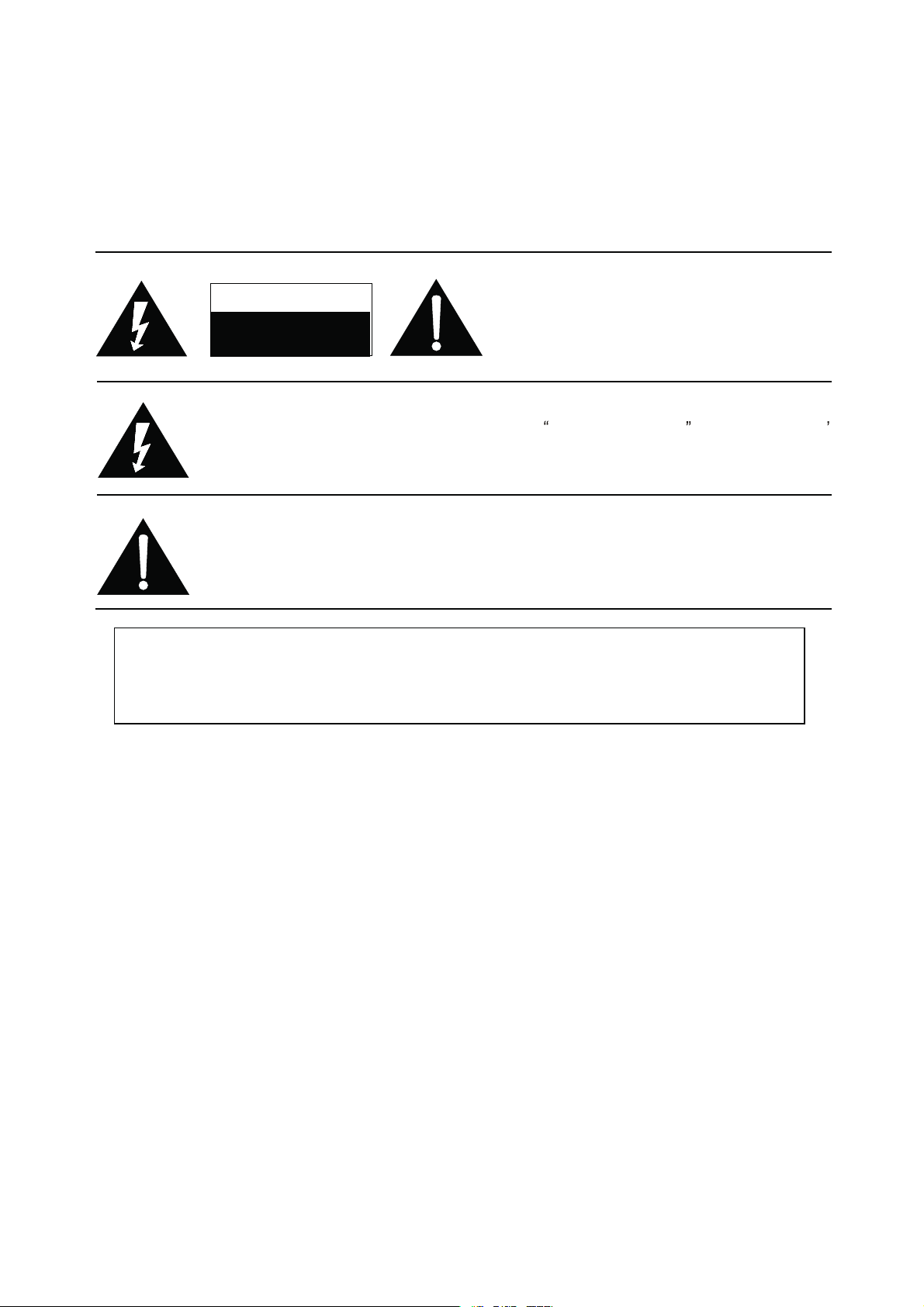
RISK OF
ELECTRIC
SHOCK DO
NOT
OPEN.
SCHNEIDER ELECTRONICS GMBH-GERMANY
1. CAUTION
CAUTION:
Use of controls, adjustments or procedures other than those specified herein may result in
hazardous radiation exposure.
CA UTION : TO RE DUCE THE RIS K OF
CA U T ION
RISK
SHOCK
The lighting flash with arrowhead symbol, with an equilateral triangle is intended to
alert the user to the presence of uninsulated voltage within the products
enclosure that may be of sufficient magnitude to constitute a risk of electric shock to
the person.
The exclamation point within an equilateral triangle is intended to alert the user to the
presence of important operating and maintenance (servicing) instructions in the
literature accompanying the appliance.
ELECTRI
NOT
OPEN.
ELECTR ICAL SHOCK, DO NOT RE MOVE
COVER (OR BACK). NO USER SERVIC EABLE
PAR TS INS IDE. RE FER SE R VICING TO
QUALIFIE D SERVIC E PE RS ONNEL.
dangerous
WARNING: TO REDUCE RISK OF FIRE OR ELECTRIC SHOCK, DO NOT
EXPOSE THIS APPLIANCE TO RAIN OR MOISTURE.
2
2
Page 3

SCHNEIDER ELECTRONICS GMBH-GERMANY
IMPORTANT SAFETY INSTRUCTIONS
CAUTION:
Read all of these instructions. Sa ve these instructions for later use . Follo w all Warnings and
Instructions marked on the audio equipment.
1. Read Instructions-All the safety and operatinginstructionsshouldbe read before the productis operated.
2. Retain Instructions- The safety and operating instructions should be retained for future reference.
3. Heed Warnings- All warnings on the product and in the operating instructions should be adhered to.
4. Follow Instructions- All operating and use instructions should be followed.
FOR YOUR PERSONAL SAFETY
1. When the power cord or plug is damaged or frayed, unplug this television set from the wall outlet and refer servicing to
qualified service personnel.
2. Do not overload wall outlets and extension cords as this can result in fire or electric shock.
3. Do not allow anything to rest on or roll over the power cord, and do not place the TV where power cord is subject to
traffic or abuse. This may res ult in a shock or fire hazard.
4. Do not attempt to ser vice this television set yourself as opening or removing covers may expose you to dangerous
voltage or other hazards. Refer all servicing to qualified service personnel.
5. Never push objects of any kind into this television set through cabinet slots as they may touch dangerous voltage
points or short out parts that could result in a fire or electric shock. Never spill liquid of any kind on the television set.
6. If the television set has been dropped or the cabinet has been damaged, unplug this television set from the wall outlet
and refer servicing to qualified service personnel.
7. If liquid has been spilled into the tele vision set, unplug this television set from the wall outlet and refer servicing to
qualified service personnel.
8. Do not subject your television set to impact of any kind. Be particularly careful not to damage the picture tube surface.
9. Unplug this television set from the wall outlet before cleaning. Do not use liquid cleaners or aerosol cleaners. Use a
damp cloth for cleaning.
10.1. Do not place this television set on an unstable cart, stand, or table. The television set may fall, causing serious injury
to a child or an adult, and serious damage to the appliance. Use only with a cart or stand recommended by the
manufacturer, or sold with the television set. Wall or shelf mounting should follow the manufacturer s instructions, and
should use a mounting kit approved by the manufacturer.
10.2. An appliance and cart combination should be moved with care. Quick stops, excessive force, and uneven surfaces
may cause the appliance and cart combination to overturn.
3
3
Page 4
SCHNEIDER ELECTRONICS GMBH-GERMANY
PROTECTION AND LOCATION OF YOUR SET
11. Do not use this television set near water ... for example, near a bathtub, washbowl, kitchen sink, or laundry tub, in a
wet basement, or near a swimming pool, etc.
Never expose the set to rain or water. If the set has been exposed to rain or wate r, unplug the set from the wall
outlet and refer servicing to qualified service personnel.
12. Choose a place where light (artificial or sunlight) does not shine directly on the screen.
13. Avoid dusty places, since piling up of dust inside TV chassis may cause failure of the set when high humidity persists.
14. The set has slots, or openings in the cabinet for ventilation purposes, to provide reliable operation of the receiver, to
protect it from overheating. These openings must not be blocked or covered.
Never cover the slots or openings with cloth or other material.
Never block the bottom ventilation slots of the set by placing it on a bed, sofa, rug, etc.
Never place the set near or over a radiator or heat register.
Never place the set in enclosure, unless proper ventilation is provided.
a built-in
PROTECTION AND LOCATION OF YOUR SET
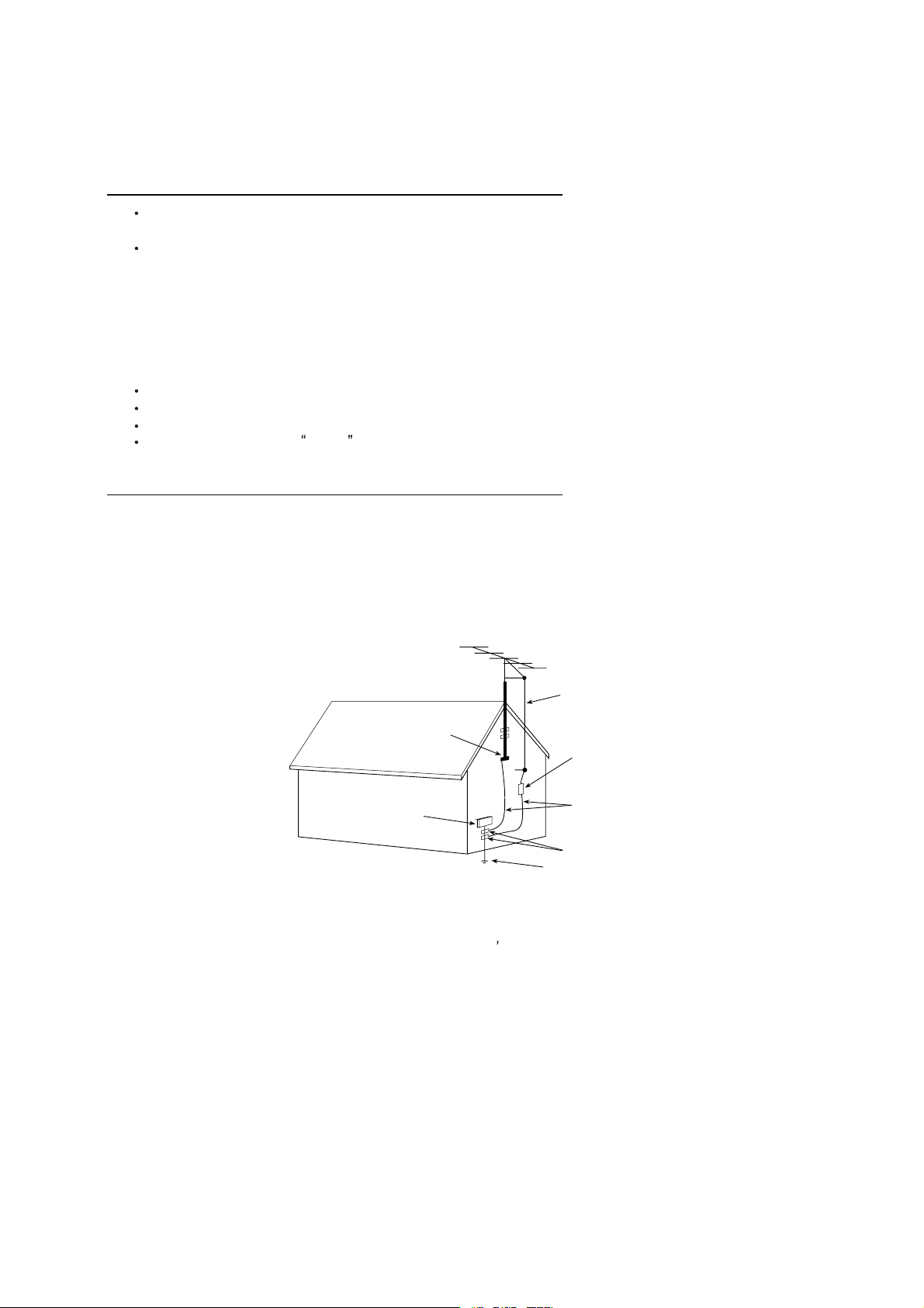
15.1. If an outside antenna is connected to the television set, be sure the antenna system is grounded so as to provide some
protection against voltage surges and built up static charges, Section 810 of the National Electrical Code, NFPA No.
70-1975, provides information with respect to proper grounding of the mast and supportingstructure, grounding of the
lead-in wire to an antenna discharge unit, size of grounding conductors, location of antenna discharge unit, connection
to grounding electrode, and requirements for the grounding electrode.
EXAMPLE OF ANTENNA GROUNDING AS PER NATIONAL ELECTRICAL CODE INSTRUCTIONS
EXAMPLE OF ANTENNA GROUNDING AS PER
NATIONAL ELECTRICAL CODE
ANTENNA
LEAD- IN WIRE
GROUND CLAMP
ELECTRIC SERVICE
EQUIPMENT
NEC-NATIONAL ELECTRICAL CODE
ANTENNA DISCHARGE
UNIT (NEC SECTION
810-20)
GROUNDING
CONDUCTORS
(NECSECTION 810-21)
GROUND CLAMPS
POWER SER VICE GROUNDING
ELECTRODE SYSTEM
(NEC ART 250. PART H)
15.2. Note to CATV system installer : (Only for the television set with CATV reception)
This reminder is provided to call the CATV system attention to Ar ticle 820-40 of the NEC that provides
installer s
guidelines for proper grounding and, in particular, specifies that the cable ground shall be connected to the grounding
system of the building, as close to the point of cable entry as practical.
16. An outside antenna system should not be located in the vicinity of overhead power lines or other electric lights or power
circuits, or where it can fall into such power lines or circuits. When installing an outside antenna system, extreme care
should be taken to keep from touching such power lines or circuits as contact with them might be fatal.
17. For added protection for this television set during a lightning storm, or when it is left unattended and unused for long
periods of time, unplug it from the wall outlet and disconnect the antenna. This will prevent damage due to lightning
and power-line surges.
4
4
Page 5

SCHNEIDER ELECTRONICS GMBH-GERMANY
OPERATION OF YOUR SET
18.
This television set should be operated only from the type of power source indicated on the marking label.If you are not
sure of the type of power supply at your home, consult your television dealer or local power company. For television
sets designed to operate from battery power, refer to the operating instructions.
19. If the television set does not operate normally by following the operating instructions, unplug this television set from the
wall outlet and refer servicing to qualified service personnel. Adjust only those controls that are coveredin the operating
instructions as improper adjustment of other controls may result in damage and will often require extensive work by a
qualified technician to restore the television set to normal operation.
20. When going on a holiday : If your television set is to remain unused for a period of time, for instance, when you go on
a holiday, turn the television set and unplug the television set from the wall outlet.
off
IF THE SET DOES NOT OPERATE PROPERLY
21. If you are unable to restore normaloperation by following the detailed procedurein your operatinginstructions,
do not attempt any further adjustment. Unplug the set and call your dealer or service technician.
22. Whenever the television set is damaged or fails, or a distinct change in performance indicates a need for
service, unplug the set and have it checked by a professional ser vice technician.
23. It is normal for some TV sets to make occasional snapping or popping sounds, particularly when being
turned on or off. If the snapping or popping is continuous or frequent, unplug the set and consult your
dealer or service technician.
FOR SERVICE AND MODIFICATION
24. Do not use attachments not recommendedby the television set manufacturer as they may cause hazards.
25. When replacement parts are required,be sure the service technician has used replacementparts specified
by the manufacturer that have the same characteristics as the original part. Unauthorized substitutions
may result in fire, electric shock, or other hazards.
26. Upon completion of any service or repairs to the television set, ask the ser vice technician to perform
routine safety checks to determine that the television is in safe operating condition.
5
5
Page 6
EM BUSINESS CENTER
FTV PRODUCT PLANNING DEPT.
SPECIFICATION RELEASE
Version: V1.0 Issued Date: 2012.12.26
Model: L39F3300F/MS63F-LA/LVF390CMTM E20
PICTURE
Panel Size (inch) 39'
Category LED TV(LED BACK LIGHT)
Aspect Ratio 16:9
Color Temperature Warm / Standard / Cold SIGNAL FORMAT CAPABILITY
Backlight Adjustable Yes Component Video Format Y,Pb/Cb,Pr/Cr:up to 720p,1080i,1080p @50Hz/60Hz
Scaler Mode Auto, 4:3, Cineme,Subtitle,Full Screen DVI Video Format Up to XGA for HDMI-PC
Picture Effect StandardˈVividˈsoftˈUserˈ HDMI Video Format Up to 720p,1080i,1080P
Picture Enhancement PC Compatibility VGA: up to UXGA@60Hz
Comb Filter 3D TERMINALS
Core Technology
MstarAC E Ye s YPbPr Input
Motion Compensation Yes Audio Input for YP bPr
DLTI Yes YCbC r Input
DCTI Yes Audio Input for YC bCr
Dynamic Skin To ne Correction Yes VGA Input(RGB)
DNR Yes Audio Input for RGB
Panel Specification DVI
Panel supplier CMI LAN
Display Resolution 1920*1080 HDMI 1.3+CEC
Brightness (cd/m2) 300
Contrast Ratio 3000:1
Response Time 8ms (G to G) RF Input
Viewing Angle (H/V) 178°/178° USB 2.0
Life Time 50000hrs Earphone
Color 16.7M (8 bit) Basic Info.
SOUND TV System ATV:NTSC PAL/M PAL/N DTV:ISDB-T
Speakers Integrated speakers (Bottom side) AV System
Audio Power Output 8W*2 TV Channels (Analog)
Sound Processing
Dolby Virtual Surround
AVC (Auto Volume Control)
SRS
Sound Features MTS, AVC, Equalizer, Surround Power Consumption-TV on
Sound Control Volume, Balance,
Function Default Color of Front Cabinet
Subtitle Yes Keyboard Position
Clock/Timers Yes Base Stand Detachable
Parent Lock Yes Unpackaged Dimension for Main Body (L*H*D) (mm)
OSD Language E nglish/Portuguese With Base Stand (mm)
OSD Features Semi-transparent Without Base Stand (mm)
HDMI CEC Yes Packaged Dimension (L*H*D)
USB Connection Yes Main Body (mm)
Demo Function Yes Base Stand
GINGA Yes Net W eight (Kg)
Picture Freeze Yes Gross Weight (Kg)
IPTV FEATURE Container Loading
Browser Opera 2.0 20 feet
NETFLIX NETFLIX3.1.4 40 feet
YouTube V3 40 feet high
Terra TV Yes ACCESSORIES
DLNA DLAN DMP 1.5 Operation Manual
Wi-Fi IEEE Standards 802.11 g/n Remote Control
Software Upgrade HUAN Base Stand
Social Network Facebook & Twitter Speaker Box
Online Picture/Album Picasa Wall Mount
High-quality scaling engine & 3-D video de-interlacer Audio/CVBS Input (Composite)
Audio/CVBS Output (Composite) 1(R/L+CVBS)
SPDIF
BTSC (SAP, Stereo, Mono) TV Channels (Digital)
MS10(DD+,DP)
Yes
Yes
Chassis
Certification
Power Supply
Power Consumption-Standby
USB Dongle
Others
2 R/L+2 Video: AV1, AV2(Bottom)
1
1˄Share with AV1˅
Share with "YPbPr"
Share with Audio for "YPbPr"
1 (D-Sub,1 5 Pins)
1˄Share with AV2˅
VKDUHZLWK³+'0,´SRUW
1
3
1 (Coaxial)
2 (Antenna, Cable)
2
1
PAL,NTSC
Cable (1125), Antenna (269)
Antenna (769)
MS63F-LA
CB
AC 100V-240V 50/60Hz
90W
Less than 0.5W
BLACK
Side
Yes
889.0×231.0×586.3
889.0×91.5×529.2
1108*200*660
Packaged with Main Body
12
13.5
180
366
488
English(Default)
For TV control (with two batteries)
Packaged with Main Body
Integrated
WMB 331
Yes(TP-LINK)
AC Power cord,AV Adapter cable
Drafted by:jiang yang 2012-12-26
Approved by:
Design and specifications are subject to change without notice! Page 1 of 1
Page 7

Factory Test & Alignment Specification For MS63F-LA Series (V0.10)
TCL World-Wide R&D
FPD CENTER
Factory Test & Alignment Specification
(FTAS)
for MS63F-LA Series
Version 0.10
PREPARED BY : Jianwei Li DATE : 2012-09-12
APPROVED BY : _____ DATE :
Page 1 of 18
Page 8
Factory Test & Alignment Specification For MS63F-LA Series (V0.10)
Disclosure
The information contained in this document is proprietary to TCL SZ FPD lab and shall
not be disclosed by the recipient to third persons without the written permission of the
team leader or GM of R&D.
Revision History
Version Issue Date Description of changes
v0.10 2012-8-12 This is the draft version of normal SIACP
·HDMI as the main absolute input
·The password of factory menu is 9735
Page 2 of 18
Page 9
Factory Test & Alignment Specification For MS63F-LA Series (V0.10)
These chassis are designed for Latin America(LA) markets Ready for IPTV. The main chip is from
Mstar and supports below features matrix:
Class Item MS63F-LA
ATV
( PAL M/PAN N/ NTSC)
DTV
(ISDB-T)
HDMI
(480i/p, 576i/p, 720p up to 1080i/p, compliant v1.4
with HDCP)
VGA
VGA/DVI audio
Inputs
&
Outputs
CMP
(YPrPb can support from 480i up to 1080p,audio)
AV 1
(CVBS ,audio)
Side AV
(CVBS,audio)
AV O U T
USB thumb drive
Headphone output
SPDIF output
OAD
WIFI Ready
DIVX
DLNA (DMP)
Functions
Internet
3D (auto, top & bottom, side by side, frame
sequencing, …)
1920x2205@24Hz (1920x1080p x2)
1280x1470@50Hz (1280x720p x2)
1280x1470@60Hz (1280x720p x2)
Audio Return Channel (ARC)
Serial connector
VGA connector
I2C connector of MEMC module
Others
Main SW Serial NAND Flash
BIN image
IC Details
&
Main EEPROM
Position
VGA connector pinout:
VGA/P508 Pin4:RXD VGA Pin11:TXD
CABLE&ANTENNA
ANTENNA
3
1
1
1
1
1
1
2
- Picture,Video,Audio Playback
- Hub, Mouse, Keyboard rd
1
Optical
•
USB Dongle accessory
(IEEE 802.11 b/g/n)
•
•
Opera
Passive Glasses
•
N/A
P508
N/A
U301
V8-6328L01-LF1Rxxx
U302
Page 3 of 18
Page 10
Factory Test & Alignment Specification For MS63F-LA Series (V0.10)
INFO:
ª All tests and measurements mentioned hereafter have to be carried out at a normal mains voltage
(220 ~ 240 VAC)
ª All voltages have to be measured with respect to ground, unless otherwise stated
ª All final tests have to be done on a complete set including LCD panel in a room with temperature of
25+/-7°C
ª The Picture Performance assessment such as White Balance (luminance and color temperature)
has to be performed into subdued lighted room after at least 45min of warm-up in order to avoid any
temperature drift influence (colorimetry vs time)
1. PCB/SKD Assembly: Test & Alignment
1.1. Pre-Conditions and DC/DC Check
Before power-on, please check the board according to the relevant block diagram and circuit
diagram, and make sure that no serious issue or mistake can destroy the board. For example, the
output of DC/DC and LDO should not be shorted to ground.
Supply a suited voltage and power-on, then check the voltage according to the relevant block
diagram, circuit diagram and voltage spec . the error should less than 5% .For example, the voltage
for main chip(+3V3, AV3.3, +1V2, CORE1V2, etc.), the voltage for DDR (DDRV) , the voltage for
amplifier (AMP_VCC), etc...
Position Value Remark
U200(U200A)
U201
U202
U203
U204
U205
U208
U209
Here enclosed circuit diagram:
3.3V ±5%
2.5V ±5%
1.5V ±5%
1.2V ±5%
5V ±5%
12V ±5%
1.2V ±5%
3.3V ±5%
3V3
2V5
1V5
1V2
5V
12V
DEMO_1V2
TU_3V3
'?⭥䐟മ?06?
06/$0$&+*
1.2. SW Image download
Download the latest release SW from below FTP server:
- Link: http://sw.tcl-cctv.com
- User name: TCL_HW_MS6328
- Passw ord: to be requested!
Page 4 of 18
Page 11
Factory Test & Alignment Specification For MS63F-LA Series (V0.10)
Æ
In case of starting from blanked flash, it’s necessary to write first “V8-6328L01-LB1Rxxx” file.
Then, following files need to be written down:
- “MS6328LA_FULL_UPGRADE.bin”
See Appendix n “How to upgrade FLASH SW using Mstar tool”
See Appendix
o “How to upgrade FLASH SW using USB”
1.3. Project ID Modification
There are different IDs stored into the NVM depending on different Panels settings and Models
features, but there’s only one key branching ProjectID that includes all. So, it’s not recommended to
modify Panel ID with Hyper terminal as other ID features may not change!
To modify Project ID, you need to go through “Design menu
spin left or right with RCU “Zoom±” keys to suitable ID (Project name is dynamically refreshed).
Service menuÆProject ID”, then
See Appendix
Here below is none exhausti ve ProjectID table for reference:
MODEL
L32E5300 001
L46E5300F 002
L42E5300F 003
L42D4330F3D 004
L39E5300F/CMI 005
L39E5300F/AUO… 006…
p “How to change Project ID with RCU”
ProjectID Panel Name
1.4. Functional Test
Once the boards (chassis, KB, IR, PSU…) and the panel are well interconnected, plug all
external generator devices to relevant inputs/outputs below according to their respective test patterns
format and check picture content and sound quality accordingly:
Source Test Signal Test Pattern
Analog /Digital Tuner
(VHF/UHF & CATV)
SPDIF (optical)
AV 1 IN
(CVBS & AUDIO)
AV 2 IN
(CVBS &AUDIO)
VGA
2D - Movie 1280x720
2D - Static Picture 1920x1080
RF cable generator
Audio Amplifier PCM or Dolby D+
Chroma/Fluke
generator
Chroma/Fluke
generator
Chroma/QuantumData UXGA - 1600x1200@60Hz
Page 5 of 18
1. Frequency Range: full band
2. Standard: NTSC /PAL M
3. ISDB-T
PAL Half Color & Gray bars
PAL Half Color & Gray bars 720x576
Half Color & Gray bars
Page 12

Factory Test & Alignment Specification For MS63F-LA Series (V0.10)
(VGA&AUDIO) generator Half Color & Gray bars
CMP via mini jack adaptor
(YPrPb & Audio)
HDMI
(Video & Audio)
RJ45
(LAN)
Headphone via mini jack adapter
Loud Speakers / Enclosures
AV OU T
(Video & Audio)
Audio tones can be defined by the factory (ie: 1KHz & 3KHz, sweep, …).
Picture video formats can be changed by the factory according to their own standard.
Remark˖1.CMP Audio in shared with AV1.
2.VGA Audio in shared with AV2.
Chroma/QuantumData
generator
with beyond HDMI 1.3
and HDCP compliant
DVD/BD player
DHCP Server ICMP packets echo request
RF signal Suitable channel
RF signal Suitable channel
RF signal Suitable channel
1920x1080i@60Hz
Half Color & Gray bars
2D - Movie 1280x720i@60Hz
3D - Movie 1920x1080@p24Hz
1.5. AD Calibration Test
As SoC as built-in A/D self-calibration mechanism, there’s not any ADC to perform.
1.6. DDC & EDID & T-Link Test
The E-EDID data structures are according to VESA Enhanced EDID 1.3 (and EIA/CEA-861B for
HDMI). CEA Timing Extension structure has been extended to support all 3D capable timings.
All VGA and HDMI structures have their own BIN profile which are part of main SW and uploaded
at power-on into HDMI switch chipset:
For EDID check, it’s needed to check whether the correct EDID is downloaded by checking
corresponding EDID NVM Checksum or read them out to check bit by bit if it is in line with the
released EDID bin file.
1.7. HDCP Test
For HDCP compliancy, it’s needed to check whether the HDCP key has been well set.
1.8. LAN/WLAN Test (MAC address and Device/User ID codes)
MAC Address Upgrade
See Appendix s“How to upgrade MAC Address
DeviceID (DID) and UserID (UID)
Purpose is to allow Other Newtork Download (OND) and further specific Services over dedicated
portal based on UK.
Description/Portal Links/Flow chart are welcome ?
For such, specific DID (32 bytes) and UID (8 bytes) needs to be paired and overwritten into
Page 6 of 18
Page 13

Factory Test & Alignment Specification For MS63F-LA Series (V0.10)
Æ
Æ
v
memory for internal client encryption.
Here are below codes examples:
Device ID User ID
BE4F255BBD106BC8F806AE456350D91F 3546187
Those DID/UID codes can only be set using UART commands following enclosed SIACP
requirements (rev. v3.9).
SIACP v3. 9
(EN_20110613).pdf
See Appendix u “,QVWUXFWLRQVRI8pdating DID,UID and MAC”
LAN Test
A rough LAN test can be done by connecting DHCP server to TV’s RJ45 and check that IP,
subnet mask, DNS addresses, … are visible on “User menuÆ
SettingÆ
More in-depth test can be performed faster using suitable UART/IR commands following SIACP
requirements. SW will internally manage Network ID (NID) flag controlling all MAC/DID/UID
integrity to facilitate PA screening further.
Note:
Cabal NetworkÆÆOK” (ensure that “Internet Connection” is Enabled at first).
It’s not necessary to check video and audio from DLNA server.
SettingÆÆNetwork
See Appendix
v
“NETWORK CONNECTION AND TEST”
2. Product Assembly (PA): Test & Alignment
2.1.Factory Menu
Follow the below steps to pop-up the Factory menu in case of “FactoryKey” is disabled:
- Press RCU “MENU” key to display main menu
- Select “Setting” and press “OK” key to enter into Setting submenu
- Select “Picture” and press “OK” key to enter into Picture submenu
- Scroll down to “Contrast” item
- Press the subsequence RCU keys “9”, “7”, “3” and “5”
In case of “FactoryKey” is enabled, just press RCU “Return” key to pop-up again the Factory
menu.
The status of “Factory Key” can be changed in Factory Menu->Hotkey.
Press RCU “OK” key or “RIGHT” key to enter the submenu.
Press RCU “Menu” key to go back to the root menu.
Press RCU “RIGHT”or “LEFT” key to change the values.
Press RCU “OK” key run the function.
Page 7 of 18
Page 14

Factory Test & Alignment Specification For MS63F-LA Series (V0.10)
t
Æ
Press RCU “Exit” key exit the Factory menu.
Factory Captions Info.
While “FactoryKey” is enabled, there’re some toggled display informations relative to SW,
ProjectID, ADC Status, to facilitate 100% quick screening without accessing to whatever else
menu:
Î Mboot SW Version
Î Main SW Version
Î Project ID
Î P (Production/Factory mode flag) / S (Factory UART
Parser mode flag) / W (Warm-Up mode flag)
See Appendix
“Factory Menu Description”
2.2. Warm-up Test
Following TCL standard and practices, it’s required minimum 15min of Warm-Up that can be
considered as Burn-In.
Additional Aging for W hite Balance alignment is no more necessary due to consistent Picture
Performance with Cloning usage.
This function is accessible by selecting “Factory menu
key and then leaving Factory menu. Other faster methods are available on above enclosed
SIACP requirements (rev. v3.9).
WARM-UP”, pressing RCU “Zoom+”
2.3. White Balance (WB)
White Balance Touch-Up
As some color coordinates discrepancies can be noticed from panel batches to others, it may
necessary to perform slight touch-up.
For Color temperature adjustment, switch TV on leading HDMI input where should be connected
suitable generator providing following format 1280x720p@60Hz test pattern. A 32 steps grey scale is
recommended to assess relevant colorimetry tracking and low/high light saturation points.
Page 8 of 18
Page 15

Factory Test & Alignment Specification For MS63F-LA Series (V0.10)
Make sure that Picture Preset is set to “VIVID” mode, “Contrast” bargraph is set to maximum
(100%) and “Active BackLight” is set to “Off”.
Ensure that TV is in
scroll down to toggle off “Pic. Enhance” flag.
PC VGA, CMP YPrPb, RGB, CVBS_PAL Gain/Offset matrix offsets locations are relative to
HDMI/DTV.
CVBS_SECAM and CVBS_NTSC Gain/Offset matrix offsets locations are relative to
CVBS_PAL.
Warm and Cool Tone are relatives to Normal mode.
Factory mode to access to ”W hite Balance” adjustment subm enu, then
¾ “Gain” registers set need to be adjusted at 70IRE.
¾ “Offsets”
defaulted.
Note:
All matrix offsets locations can be individually fine-tuned.
registers set can be adjusted at 30IRE, but it’s not recommended to keep them
Targets and Tolerances for all inputs
The measured parameters should be mainly “x”, “y” coordinates.
The “Y” peak luminance measurement at 100IRE is depending on achievable panel
performance and less important than saturation on high light. If necessary, “Scaling Contrast”
register can be adjusted.
The “BlackLevel” measurement need to be within 1% ±2. If necessary, “Scaling Brightness”
register can be adjusted.
The White Balance alignment should be performed using a well calibrated and contact less
analyzer (ex: Minolta CA210 or CA310). The analyzer may not touch the screen surface, and
measurement must be performed in a dark environment keeping the probe(s) at 90+/-2° from the
panel center.
The result should fulfill TCL matching specification (Minolta CA310 reference with CH00):
MODEL COOL(x/y) NORMAL(x/y) WARM(x/y)
L32E5300 275/280 280/290 302/307
L42E5300F 270/280 282/297 302/307
L46E5300F 270/280 280/295 302/307
……
……
within below tolerances:
¾
for Alignment: ± 0.003
¾
for Measurement: ± 0.015
Page 9 of 18
Page 16

Factory Test & Alignment Specification For MS63F-LA Series (V0.10)
Æ
2.4. SHOP-END Test
At final process stage, it’s necessary to perform “Reset shop” before any packing to leave
Factory mode and restore User default presets.
This function is accessible by selecting “Factory menu
key. Other faster methods are available on above enclosed SIACP requirements (rev. v3.9).
SHOP init”, then pressing RCU “OK”
Appendix n “How to upgrade SW FLASH using Mstar tool”
¾ Open Mstar “Mboot” software programming tool “ISP_Tool_4528”
¾ Click on “Read”,and select “mboot.bin”file
¾
¾ Then click “Connect”,it will check SPI FLASH’s tape----correct,it will display OK.
Page 10 of 18
Page 17

Factory Test & Alignment Specification For MS63F-LA Series (V0.10)
¾ Next,click on “Auto” menu,then click “Run”,it begin programming “Mboot.bin”,when
programming success,it will display a word “Pass”.
¾
¾
Page 11 of 18
Page 18

Factory Test & Alignment Specification For MS63F-LA Series (V0.10)
Æ
Æ
Appendix o “How to upgrade FLASH SW using USB”
There are two methods to upgrade SW using USB,the first one like below˖
¾ In the previous of upgrade SW using USB,should program mboot bin file”
V8-6328L01-LF1Rxxxbin” by ISP_Tool .
¾ Then switch off TV by removing AC cord.
¾ Copy the SW BIN image “MS6328LA_FULL_UPGRADE.bin” into USB stick (pen drive)
root path
If there’s already other “
Note:
to be deleted or renamed
¾ Plug USB stick to the TV
¾ Press and hold the power key of key board before reconnect AC cord to restart TV for
5-8seconds.
¾ Once USB stick starts blinking, TV is uploading SW BIN image.
¾ When update is successful, TV should restart automatically.
¾ Remember to perform “Factory menu
¾ Switch off TV by removing AC cord
¾ Reconnect AC cord to restart TV and wait few seconds for Eeprom update
MS6328LA_FULL_UPGRADE.bin” into USB root, it needs
NVM reset“and then press RCU “OK” key
The second method ˖
¾ To use this method,there should be SW in mainboard to ensure TV can display normally.
¾ Copy the SW BIN image “
path
¾ Press RCU MENU
¾ TV display a warning information ,that means it is upgrading,almost 3minutes later,when
upgrade successful,TV should restart automatically.
SettingÆFunctionÆsoftware upgradeÆOKÆBy USB
V8-6328L01-LF1RXXX.bin” into USB stick (pen drive) root
Appendix p “How to change ProjectID with RCU”
¾ Process following subsequence IR codes to change projectID: 062598+MENU+xxx
(xxx:ProjectID, ex: 003)
¾ Restart TV
Appendix q “How to upgrade MAC Address
¾ Upgrading MAC address need to use the tool in factory and through serial command, The
specific methods according to the operation of the factory guidance.
Appendixr“Factory Menu Description”
1-Factory hotkey submenu
Item Sub-item Value Note
)DFWRU\
KRWNH\
Off/On
OFF᧶hotkey is invalid
ON ᧶hotkey(Ret urn ke y) is av ailability
Page 12 of 18
Page 19

Factory Test & Alignment Specification For MS63F-LA Series (V0.10)
2-Warm-Up Mode submenu
Item Sub-item Value Note
Select panel On with left/right key, Press
Warm-UP
Mode
Off/On
“EXIT” key to enter the burning mode;
Press “Menu” key on keyboard to exit the
burni ng mode
3-ADC submenu
As SoC as built-in A/D self-calibration mechanism, there’s not any ADC to perform.
4-White Balance submenu
Item Sub-item Value Note
Bala nce source are˖
HDMI, VGA, DTV, PAL, SECAM, NTSC,
Scart RGB, CMP
Warm and cool value is relative to Normal
one. Normal is the default Tone mode
R W hi te balanc e ( -127..+128 for gain)
G W hite balanc e (-127..+128 for gain)
B W hit e ba lanc e (-127..+128 f or gain)
R Gray balanc e (-127 .. +128 for offset )
G Gray balance (-127..+128 for offset)
B Gray balance (-127..+128 for offset)
Press “OK” key t o ini tia l the preset RGB
Gain/Offset value
White
Balance
Source HDMI,etc
Color Temp
Normal
/Warm/Cool
R Gain 000..255
G Gain 000..255
B Gain 000..255
R Offset 000..255
G Offset 000..255
B Offset 000..255
White Balance Init DO
5-Shop init submenu
Item Sub-item Value Note
Shop Init
6-NVM Reset submenu
Item Sub-item Value Note
Reset ALL
VGA ADC Status NG
YPbPr ADC Status NG
DO
DO
Page 13 of 18
Clea r date of NVM i n use r men u,i nclude
the v alue re lated i nstallation,and Clea r
date of factory menu except the item of
Bala nce and sound ,set to default value
Clear NVM values ˈ and set to default
value
Page 20

Factory Test & Alignment Specification For MS63F-LA Series (V0.10)
7-Preset Factory Channel submenu
Item Sub-item Value Note
Preset Factory
Channel
HZ/CD/NM/W
X/POLAND
8-Power On Mode submenu
Item Sub-item Value Note
Power On
Mode
ON/LAST/STB
Preset the cha nnel t able of fac to ry.To
pres et the c hannel table of certa in
factory,firstly,choose the corresponding
factory name,then press OK button of
remot e contr ol a nd wait until the
disappearance of Factory Menu.
ON: T he s et will power o n af te r switching
on power
STB: Force TV to sta rt i n sta ndby
Last: Force TV to start from last power
status
9-USB UPDATE submenu
Item Sub-item Value Note
Main Upgrade
MEMC Upgrade
HDCP Uprade
USB
UPDATE
Mboot upgrade
NVM Upgrade
NVM backup
CH list Upgrade
CH list backup
0- DeviceID test submenu
Item Sub-item Value Note
USB Clone Mode
USB
Clone
TV TO USB DO
USB TO TV DO
All
ChannelList
EEPROM
User Setting
Upgrade software
Upgrade MEMC
Upgrade HDCP
Upgrade Mboot
Upgrade NVM
Bac kup NVM
Upgrade C H lis t
Bac kup CH list
Sele ct to choose the things you want to
clone
Press “Right” key to copy the
data (WB,ADC,pi cture sett ing,etc) to USB
Press “Right” key to set the
data (WB,ADC,pi cture sett ing) from USB
Page 14 of 18
Page 21

Factory Test & Alignment Specification For MS63F-LA Series (V0.10)
Appendix u “,QVWUXFWLRQVRI8SGDWLQJ','8,'DQG0$&”
1,use the Uart command to sent DID and MAC using the command :
DID write: B2 DATA 0 TO DATA N(ASCII )
UID write:B8 DATA 0 TO DATA N(ASCII )
MAC write:B3 MAC address 6 ˄Binary˅
The process is as the picture below:
Portal give the UID and DID to the factory local service ,and the service connect to the factory LAN.
When product line produce the IPTV , there will be a work station (PC normally) down load the DID , UID
and also MAC from the local service ,then using UART command sent them to the module.
2,How to test the function:
When there is a module need to test the Device function connect the set to the LAN use the device ID test the
module will sent the device ID information and user ID information to the local service and compare with the
data-base .so that the data is verified .
Page 15 of 18
Page 22

Factory Test & Alignment Specification For MS63F-LA Series (V0.10)
Appendix v”NETWORK CONNECTION AND TEST”
1.Network connection
You can set up your TV so that it can access the Internet through your local area network (LAN)
using a wired or wireless connection.
1.1Connecting to a wired network
You can attach your TV to your LAN using cable in three ways:
• You can attach your TV to your LAN by connecting the LAN port on your TV to an external modem
using a Cat 5 cable.
• You can attach your TV to your LAN by connecting the LAN port on your TV to a IP Sharer which is
connected to an external modem. Use Cat 5 cable for the connection.
• Depending on how your network is configured, you may be able to attach your TV to your LAN by
connecting the LAN port on your TV directly to a network wall outlet using a Cat 5 cable. Note that the
wall outlet is attached to a modem or router elsewhere in your house.
Select Options > Network > Configuration >Interface, then select Ethernet to connect to a wired
network.
1.2 Connecting to a wireless network
To connect your TV to your network wirelessly, you need a wireless router or modem and a Wireless
LAN Adapter. Connect your Wireless High Gain USB
Adapter (USB dongle) delivered with your TV to your TV’s USB 1 port.
1.2.1 Select Options > Network > Configuration >Interface, then select Wireless to connect to a
wireless network.
1.2.2. Select Wireless setting and press OK/• to enter.
1.2.3. Connection Methods: You can setup the wireless network connection three ways.
1.2.3.1 Scan
• Select Wireless setting > Scan, then press OK/• , the TV will scan all access points within range.
The access points found by the TV will be displayed.
• Select an available access point, then press OK/• to connect the TV to it.
Notes:
- If you select a protected access point, you will have to enter the corresponding password.Press
Menu on the remote control to display virtual keyboard to enable you to enter the password.
- This set has a memory function of available access point, which enables your set to be connected
to the network even if you switch on TV after power off.
1.2.3.2 Manual
Select Wireless setting > Manual, then press OK/• , you will be prompted to enter the correct SSID
of an available wireless router to setup the connection.
-1.2.3.3 Auto
If your AP supports WPS (Wi-Fi Protected Setup), you can connect to the network via PIN (Personal
Identification Number) or PBC (Push Button Configuration). WPS will automatically configure the
SSID and WPA key in either mode. Select Wireless setting > Auto, then press OK/• to enter.
• PIN: Select PIN and press OK/• to enter. Generate a random PIN code. Make sure this code is
installed to the AP. (For the procedures, refer to your router manual.) Press OK/• again to setup the
connection.
• PBC: If your router has a PBC push button, select PBC, then press OK/• to enter. Press PBC
push button on your router within 2 EN 12 minutes after you press OK/• again. Your TV will
automatically acquire all the network setting values it needs and connect to your network.
Network setup
1. Press Menu on the remote control and select
Page 16 of 18
Page 23

Factory Test & Alignment Specification For MS63F-LA Series (V0.10)
Options > Network > Configuration > Internet connection. Press • /• to select On. Wait until the
connection is automatically established.
2. Select Options > Network > Configuration >Connection test, then press OK/• to check the
Internet connectivity. If fail, follow below step to make sure the connectivity.
3. Select Options > Network > Configuration > IP setting, then press OK/• to enter the IP setting
menu.
- Set Address type to Auto, it will acquire and enter the needed IP address automatically.
- You can follow below steps to enter your IP address manually.
• Set Address type to Manual, then press • to go to the first entry field.
• Enter the IP address, Subnet mask, Default gateway, Primary DNS and Secondary DNS values.
Use the digit buttons to enter numbers and the arrow buttons to move from one entry field to another.
- After setting, select Options > Network > Configuration > Connection test to check the Internet
connectivity again.
4. Select Options > Network > Configuration> Information, then press OK/• to display the
information on current connection, such as Interface, Address type, IP address, etc..
Share & See
Note: This manual covers products with either Share& See or DLNA function. Share & See is DLNA
compatible.
Connecting to your PC
Make sure to set up a wired or wireless connection from your TV to a router first. Then connect your
PC to your router either through a network cable or wirelessly. Follow the steps in turn specified
hereafter, then you can enjoy recorded video, picture, music and/or text files saved on your PC.
Adding media from your PC for sharing
Install a DLNA media server in your PC. The simple and familiar server you may install is Microsoft
Windows Media Player 11. Allow your TV to share the designated files on your PC.
1. Open Microsoft Windows Media Player 11.
- Select Library > Media sharing.
- Check the checkbox Share my media to.
- Select the icon of the TV set connected to your PC.
- Select Allow to allow the TV set to access your PC, and select OK to enable your allowing.
Note: You can push Settings button to customize your desired settings.
2. - Select Library > Add to Libray.
- Select your personal folders or folders of other users that you can access for sharing.
- Select Add and press OK to enable your adding.
Share & See application
1. Select Options > Network > Applications > Share & See
, then press • /• to select On.
2. Press Menu on the remote control and select USB, then press OK to launch Share & See
applications.
Stopping Share & See function
1. Select Options > Network > Configuration >Internet connection, and set it to Off.
2. Or select Options > Network > Applications >Share & See, and set it to Off.
Opera browser
This feature brings desired contents and services directly from the web to your TV.
Notes:
- Configure the network settings before using this feature.
- Unsupported fonts within the provider’s content will not display normally.
- Slow responses and/or interruptions may occur, depending on your network conditions.
1. Press Option on the remote control and select Quick access > Opera.
Page 17 of 18
Page 24

Factory Test & Alignment Specification For MS63F-LA Series (V0.10)
Positon
3$57
7<3(
Part Number
6:
2. Press OK to display the homepage of your browser.
3. Use • /• /• /• on the remote control to navigate through the webpage, and press OK on the
remote control to confirm an entry or selection. You can also press Menu on the remote control to
access or exit virtual keyboard. Connect your wired or wireless mouse through your TV’s USB jack.
Use your mouse to navigate within the webpage.
Home: Click it to display the homepage.
Back: Return to the webpage you just left.
Go to: Select from the list to get back to a recently visited webpage.
Refresh: Click it to refresh the webpage.
Bookmark manager: Click it to display the Bookmark manager.
English
- Add a folder: Add folders to your Bookmark manager so as to organise your bookmarks into
folders to include all the websites you visit frequently. Click Add a folder bar, type a name for the
folder, and then click Ad d . Repeat this step until you have created as many folders as you’d like.
- Visit a bookmark: Go to a bookmark by simply clicking its name, instead of having to type its
address.
- Delete a bookmark: Click the Delete icon after a link to delete the link if you want to.
- Edit a bookmark: Click the Edit icon after a link to edit the name and/or URL of the bookmark if
you want to.
- Click Close bookmark manager bar to close.
Add a bookmark: Go to the webpage you want to add to your Bookmark manager and click Type a
new name for the webpage if you want to, specify the folder that the bookmark should be created in,
then click Ad d .
Notes for password in Parental Control Lock function:
- The default password is 1234. You can change it to a new one.
- The super password is 0423. If you forget your code, enter the super password to override any
existing codes.
Appendix
u “,QVWUXFWLRQVRI8SGDWLQJ6:”
7KHIROORZLQJ,&VKRXOGEHSUHFRSLHGEHIRUH607SURFHVV
7
8 62- 13-W25Q16-00B˄CPP˅
8 ,&-762
3
13-FHMT29-4GB(CPP)
MBOOT:
V8-6328L01-LB1Rxxx
0DLQ6RIWZDUH˖
V8-6328L01-LF1Rxxx
7KH'(9,&(,'0$&$GGUHVV+'&3.(<(61.(<PXVWEHXSJUDGHE\GXEXJSRUWLQWR8.
Page 18 of 18
Page 25

R
Amplifier
R
E
W
O
P
S
D
V
L
DDR2
Y
E
K
R
I
DDR
IPTVDDR1
MS6328
LVDS
Flash
TS
FLASH
DEMO
USB
TMDS
VGA
YPbPr
CVBS
IF
Audio
IR
L
TS8121
Page 26

7
65432
1
D D
MSD6328BX TCL DESIGN
PAGE1 INDEX
PAGE2 TUNER
C C
PAGE3 POWER SUPPLY INTERFACE
PAGE4 MSD6328
PAGE5 DDR
PAGE6 YPBPR/AV IN/VGA IN
PAGE7 HDMI SWITCH
PAGE8 USB&LVDS
PAGE9 AMPLIFIER
PAGE10 ISDB
B B
A
THIS DRAWING CANNOT BE COMMUNICATED TO UNAUTHORIZED PERSONS COPIEDUNLESS PERMITTED IN WRITING
7
6
SHENZHEN V0.1
...
...
...
18-SEP
...
DD-MM
DD-MM
DATE DESCRIPTION Last modifNAMEIndex-Lab
...
...
Last saved :
INITIAL VERSION 18-SEP
...
...
...
7-16-2012_14:17
...
...
...
SBU :
TCLNO:
.............
...
DESIGNATION
INDEX
ADDRESS1
ADDRESS2
ADDRESS3
TELEPHONE
ON:
BY:
DRAWN
TCL
CHECKED
DD-MM-YY
ON:
BY:
......
PAGE:
1
OF :
25
FORMAT DIN A4
MT5311B
Page 27

8765432 1
TU_3V3
T
TU_3V3
C101
100U
16V
C102
0.1U
R101
AD2RF_SW
1M
T
T
AIR
AIR
3
TU_3V3
F101
1
RF_SW
R102
33K
0BAV99
D102
C114
2
C1150.047U
987
GND6
RF2
GND5
U103
GND1
RF1
312
GND4
RFC
GND3
GND2
C2
10
C1
11
VDD
12
GND8
GND7
GND6
GND5
GND4
GND3
GND2
GND1
R100
NC/0R
0.01U
C103
TUNER_GND
10
9
8
7
6
5
4
3
S2
2
S1
1
T
CABLE
3V3
F
E
TU101
D
0.047U
CABLE
3
F102
1
0BAV99
D101
2
IF_AGC
T
TUNER_IF_AGC
C
TU_3V3
R121
R126
4K7
4K7
B
TUNER_CLOCK
TUNER_DATA
C135
10P
A
GND
R124 NC/100R
R125 NC/100R
C136
10P
R122
100R
R123
100R
T_SCL
T_SDA
OSCL0
OSDA0
C134
0.047U
GND
THIS DRAWING CANNOT BE COMMUNICATED TO UNAUTHORIZED PERSONS COPIED UNLES S PERMITTED IN WRITING
6
5
4
PE42750
R115
TU_3V3
10R
TU_3V3
C104
C106
C105
0.047U
0.047U
0.047U
L101
NC/330NH 140MA
R171
10K
DD-MM
...
...
DD-MM
DD-MM
...
DD-MM
...
DATE DESCRIPTION Last modifNAMEIndex-Lab
Last saved :
C1070.047U
C141
82P
NC/0R
Q132
BT3904
R117
C
R172
GND
...
...
...
...
100K
100P
C108
A_IF_AGC
E
BT3906
B
Q131
C
B
E
...
...
...
...
4-14-2009_15:30
10P
C109
1000P
C110
150P
C116
L102
220NH 120MA
R173
100K
45678
TU_3V3
BT3904
TU_3V3
C117
82P
TUNER_CLOCK
TUNER_DATA
NC/0R
C
R175
R174
10K
C
Q134
B
E
GND
R116
100K
...
...
...
...
B
FAT+_D
E
BT3906
Q133
10K
FAT-_D
R103
0R
R198
NC/0R
R176
SBU :
TCLNO:
.............
D_IF_AGC
Close to SoC
L103
2.2NH
C129
0.22U
39
383637
CAPRFAGC
RFAGC_SENSE
UHFSUPPLY
UHFHIGH
VCC1-RF
1
RFIN
2
NC1
3
NC2
4
GND1
5
AS_XTSEL
6
GND2
7
TEST1
8
TEST2
9
GND3
10
R111
33R
33R
R112
IF-AGC-SEL
DESIGNATION
...........
30P
SCL
SDA
11
C131
TDA18273HN
XTALP
GND4
13
12
X16M1
16M
33R
L1058.2NH
2.4NH L104
0.1UC130
TU_3V3
3534323331
UHFLOW
VCC2-RF
VHFHIGH
VHFSENSE
U102
TDA18273HN
GND5
CAPREGVCO
VCC-SYNTH
XTALN
174020
16
15
14
0.1U
TU_3V3
C121
30P
R104
33R
R105
L106
100NH
VHFLOW
VHFSUPPLY
VSYNC
VIFAGC
VCC-IF
XTOUT2
XTOUT1
VTUNE
CP
18
19
6.8N
C122
C132
GND7
GND6
IRQ
IFP
IFN
C153
30
29
28
27
26
25
24
23
22
21
ADDRESS1
ADDRESS2
ADDRESS3
TELEPHONE
DRAWN
ON:
BY:
120P
TUNER_IF_AGC
C127
C128 1U
T
XOUT
2.7N
C123
R109
56R
R107
56R
TU_3V3
1U
NC/47P
XOUT
C125
R110
430R
C124
TCL
CHECKED
DD-MM-YY
ON:
BY:
......
NC/47P
C126
0.22U
PAGE:
OF :
123
FORMAT DIN A3
D_IF2
D_IF1
FAT+_D
FAT-_D
F
E
D
C
B
A
Page 28

876554321
C225
GND
GND
GND
2U2
R242
220R
12
11
10
9
D2B
5
D2A
6
D1B
7
D1A
8
R2391K
R240
33K
L201
8U2
C210
10U
C243
390P/NC
10R
R223
R224
C256
1000P
GND
C263
0.1U
L215
1UH
C267
10N
54418 VREF=0.8V
54519 VREF=0.6V
G5193 VREF=0.827V
DIM_DC
C244
U204
P202
10N
0R/NC
R24
0R/NC
R25
1
2
3
4
LGATE
GNDPHASE
1
2
3
4
VCC
BOOT
VIN
EN
SS
47K/NC
VIN1
VIN2
GND1
GND2
C221
R257
1
34
56
78
9
1112
C226
0.1U
VSENSE
TPS54331
U205
f=570KHz
GND
1
2
36
4
C269
NC/10N
24/12V
GND
GND
COMP
C206
VIN3
AGND
24/12V
0.1U
PH
2.2U
GND
16
TPS54319
TPS54418
5
R256
20K
T
GND
DIM_IN
8
7
6
5
GND
15
EN
U203
VSENSE
6
GND
3V3SB
DIM_PWM
GND
R207
68K
C246
3300P
R251
33K/NC
14 7
PWRGD COMP
GND
C268
G2
4
S2
3
G1
2
S1
1
Q201
BOOT RT/CLK
3300P
T
T
C249
0.01U
D204
SR34
GND
AO4822A
13 8
R255
150K
3V3SB
GND
PH3
PH2
PH1
SS/TR
T
24V
F
VBL_CTRL
R238
GND
DIM_DC
POWER_ON
R241
330R
10K
0.01U
C247
P_ON
2
T
T
BL_ON
T
GND
10
BL_ON
C250
0.01U
C248
0.01U
GND
E
24/12V
(vin=3.5V~28V)
C219
24/12V
D
0.1U
GND
24/12V
C
B
5V
C261,C262 must connect PIN3,4,5
A
All above are PIN to PIN
f:adjustable 300kHz~2MHz ,set f=1.1MHz
Caution:
G5193:RD3=20K
54519:RD4=33K,f=1.1MHZ
G54418:RD3=12K
BOM COST=1.55RMB(5193)
C202
2.2U/50V
R209
22K
12V
C231
0.1U
TPS54418:4A
TPS54519:5A
RD3=20K
R208
100K
GND
C232
0.1U
GND
5V
(vin=2.95V~5.8V)
C261
10U
G5193:3A
C245
NC/1N
C205
2.2U/50V
D205
8
7
VIN
5
BOOTFBUGATE
C262
0.1U
LL4148
RT8110B
f=400KHz
GND
THIS DRAWING CANNOT BE COMMUNICATED TO UNAUTHORIZED PERSONS COPIED UNLES S PERMITTED IN WRITING
GND
10R
C264
0.1U
GND
BRI_ADJ
C201
10U
VREF=0.8V
L202
10UH
C200
16V
220U
VREF=0.8V
22U
GND
3DSELECT
C220
0.1U
C258
10U
GND
22U
C266C265
R271
10K
3D ENABLE:3DSELECT=H
12V
T
12V
@max 3A
R206
39K
R205
2K7
GND
C234C233
10U
C209
0.1U
0.1U
1V2
T
100R
R266
0R
R252
6K8
R253
12K
R254
3K3
GND
R265
B
5V
T
R225 3K3
R226
560R
47R
GND
@max 3A
5V
R272
3K3
C
BT3904
R274
Q207
E
470R
R275
470R
C255
150P
R227
VCC_VSENSE
3D-DIM
B
BRI_ADJ
BT3904
3V3SB
GND
T
100R
R273
C
Q209
Q208
E
E
C
BT3904
2
3
4
P203
B
PWR-ON/OFF
1
LVDS24PIN
16V
3V3SB
C213
100U
C257
0.1U
GND
R243
3K3
R244
330R
POWER_ON
5V
U209
LD1117S33
4
4
GND/ADJ
OUT
VIN
123
TU_3V3
C271
C272
10U
0.1U
GND
U208
AS1117AD
3V3
C288
DTMB-1V2
T
4
4
GND/ADJ
OUT
VIN
123
0.1U
R285
120R
C289
DEMO_1V2
C287
0.1U
2U2
F
E
D206
1
DRAWN
R237
47K
C240
1000P
2
GND
5V
F200
GND
3V3SB
KEY
C236
GND8
T
TT
1
2
3
4
C222
0.1U
0.1U
T
+5V
GND
GND
IR
3V3IR
TT
T
C235
0.1U
3V3KEY
KEY
C223
1000P
TCL
CHECKED
DD-MM-YY
ON:
BY:
......
P201
3VSB
IR
STBY_LED
SENSOR
PAGE:
OF :
D
1
2
3
4
5V
5
6
7
P200
T
GND2
C
B
A
0BAV99
3
GND
close to SOC
R210
10K
F210
0.1U
C224
GND
5VKEY
GR
T
T
T
C237
0.1U
C239
1000P
GND
ADDRESS1
ADDRESS2
ADDRESS3
TELEPHONE
ON:
BY:
U202
R200
3R9
R222
NC/0R
U200
LD1117S33
4
5
PGOOD
6
DD-MM
DD-MM
DD-MM
DD-MM
DATE
PVIN
VIN
f=1.2MHz
VREF=0.8V
AS1117-2.5
Z208
C251
0.1U
MP2127
T
C212
VIN
SW
GND
FB
U201
10U
4
4
OUT
...
...
...
...
(vin=2.7V~6V)
5V
C203
C227
0.1U
10U
GND GND
5V
5V
R261
1R2
5V
R262
1V2
NC/0R
...
...
...
...
Index-Lab
Last saved :
L204
3
1UH
2
GND
1
4
4
OUT
VIN
C230
0.1U
GND/ADJ
123
C216
10U
...
...
...
...
DESCRIPTION Last modifNAME
4-14-2009_15:28
C254
0.1U
R219
33K
GND/ADJ
123
1V5
T
C228
0.1U
C204
10U
R220
33K
R221
4K7
GND
2V5
T
C229
0.1U
U200A
3V3
T
C253
10P
AZ1084
ADJ/GND
C260
1
1V5
@max 2A
C214
10U
2V5
10U
23
VOUTVIN
3V3
...
...
TCLNO:
...
.............
...
L_SENSOR
SBU :
LED_R
LED_G
IR-IN
DESIGNATION
3V3SB
4K7
R228
5V
L_SENSOR
R245
100K
power
600R
KEY0-IN
600R
LS
L209600R
L210
L206
L211600R
L207600R
L208
600R
C238
1000P
...........
4678
321
FORMAT DIN A2
Page 29

12 11 10 9 8 7 6 5 4 3 2 1
H
VCC_VSENSE
VSENSE_VSS
T
VSENSE
GND
DVDD_NODIE
G
2V5 FOR lvds
AVDD25_PGA
GND
120R
L301
F
E
D
2V5
C
2U2
C318
L300
60R
0.1U
B
Mode Selection
// CHIP Config {I2S_OUT_BCK, I2S_OUT_MCK, PAD_PWM1, PAD_PWM0}
B51_NO_EJ 4'b0000 Boot from 8051 with SPI flash
SB51_WOS 4'b0001 Secure B51 without scramble
SB51_WS 4'b0010 Secure B51 with scramble
MIPS_SPI_NO_EJ 4'b0100 Boot from MIPS with SPI flash
MIPS_SPI_EJ_1 4'b0101 Boot from MIPS with SPI flash
MIPS_SPI_EJ_2 4'b0110 Boot from MIPS with SPI flash
MIPS_WOS 4'b1001 Secure MIPS without scramble
MIPS_WS 4'b1010 Secure MIPS with scramble
R4064K7
R4144K7
R4084K7
A
R4104K7
GND
1V2
1V5
0.1U
PGA_VCOM
LED_R
I2S_BCK
I2S_MCK
3D_IN
3V3SB
1U
C315
2V5
PGA_VCOM
3V3
C374
C378
0.1U
GND
C375
0.1U
AVDD25_PGA
C376
U303
R17
R18
T18
T19
T20
T21
U19
U20
U21
U22
V22
T22
R19
P17
N15
M15
N16
P16
L8
Y6
Y7
Y8
W8
W9
Y5
Y4
M8
M5
M6
M7
N4
N6
M4
H6
N5
N7
H17
H16
J16
J17
H15
K18
L17
L18
M18
K17
J8
F8
U25
A9
A12
A15
F20
C21
D19
C25
E19
F19
E22
F25
J25
L23
D22
D7
D8
D9
D10
D11
D12
D13
D14
D15
D16
E8
E9
E10
E11
E12
E13
E14
E15
E16
F9
F11
F12
F13
F14
F15
F16
G22
G9
G11
G12
G13
G14
G15
G16
G17
G18
C377
0.1U
GND
U7U8U9
VDDC1
VDDC2
GND135
GND136
VDDC3
VDDC6
VDDC7
VDDC8
VDDC4
VDDC5
VDDC9
VDDC
VDDC10
VSENSE
VSENSE_VSS
DVDD_DDR
AVDDL_MOD
AVDD11_ETH
AVDD1P1_ADC
AVDDLV_USB
DVDD_NODIE
AVDD25_DADC
AVDD25_REF
AVDD25_REF1
AVDD25_ETH
AVDD_MOD
AVDD25_PGA
PGA_VCOM
AVDD_DMPLL
AVDD_NODIE
AVDD_DVI
AVDD_DVI1
AVDD_AU33
AVDD_EAR33
AVDD3P3_ADC_MPLL
VDDP5
VDDP
AVDD_LPLL
AVDD_DDR0_D1
AVDD_DDR0_D2
AVDD_DDR0_D3
AVDD_DDR0_D
AVDD_DDR0_C
AVDD_DDR1_D1
AVDD_DDR1_D2
AVDD_DDR1_D3
AVDD_DDR1_D
AVDD_DDR1_C
GND_FU
GND168
DDR_GND14
DDR_GND2
DDR_GND1
DDR_GND
DDR_GND7
DDR_GND8
DDR_GND9
DDR_GND6
DDR_GND10
DDR_GND11
DDR_GND13
DDR_GND5
DDR_GND4
DDR_GND3
DDR_GND12
GND19
GND7
GND8
GND12
GND21
GND113
GND18
GND100
GND114
GND115
GND101
GND24
GND22
GND23
GND25
GND116
GND117
GND102
GND26
GND27
GND58
GND59
GND20
GND118
GND119
GND123
GND173
GND120
GND121
GND122
GND124
GND125
GND126
GND127
GND130
GND111
GND112
GND178
GND149
GND150
V9
C7
V10
V11
V12
MSD6328EX
AUVRM
AUVRP
AUVAG
Close to MSTAR IC
with width trace
GND137
GND151
U10
U11
U12
U13
U14
U15
U17
U18
W19
W20
W21
W22V5V6V7V8
GND138
GND139
GND140
GND141
GND142
GND143
GND144
GND145
GND146
GND147
GND148
GND163
GND164
GND165
GND166
GND129
GND128
GND174
GND10
GND11
GND13
GND14
GND15
GND16
GND17
GND28
GND29
GND30
GND31
GND32
GND33
GND34
GND35
GND36
GND37
GND38
GND39
GND40
GND41
GND42
GND103
GND43
GND44
GND45
GND179
GND169
GND46
GND172
GND180
GND47
GND48
GND49
GND50
GND51
GND52
GND104
GND53
GND54
GND60
GND61
GND62
GND63
GND64
GND65
GND66
GND67
GND68
GND170
GND69
GND70
GND71
GND72
GND55
GND56
GND57
GND73
GND74
GND75
GND76
GND77
GND78
GND79
GND80
GND81
GND82
GND83
GND84
GND85
GND86
GND87
GND88
GND89
GND90
GND91
GND92
GND93
GND94
GND95
GND96
GND97
GND98
GND99
GND105
GND106
GND107
GND108
GND109
GND110
GND131
GND132
GND133
GND134
GND171
GND175
GND152
GND153
GND154
GND155
GND156
GND157
GND158
GND159
GND160
GND161
GND162
W4W5W6
W7
A20
V13
V14
B19
R24
W10
W11
W12
W13
W14
3V3SB
2U2
GND
DDR3 POWER
1V5
2U2
2U2
C320
C319
GND
C389
10U
10U
0.1U
C305
C304
THIS DRAWING CANNOT BE COMMUNICATED TO UNAUTHORIZED PERSONS COPIED UNLES S PERMITTED IN WRITING
GND167
GND1
GND2
GND3
GND4
GND5
GND6
GND9
GND176
C321
Close to MST IC
with wide trace
VGA-RIN
GND
R38833R
NAND & CI & TS & Front End
PCM_D0
PCM_D1
PCM_D2
PCM_D3
PCM_D4
PCM_D5
PCM_D6
H7
H8
H9
GND
D
H11
H12
H13
H14
H22
J7
V4
J10
J11
J12
J13
J14
J15
J22
K7
K9
K10
K11
K12
K13
K14
K15
K16
K20
K21
K22
L9
L10
L11
L12
L13
L14
L15
L16
J9
R22
L22
F22
M9
M10
M11
M12
M13
M14
W15
M16
M17
N8
N9
N10
N11
N12
N13
N14
V15
V16
N17
P25
N19
P7
P8
P9
C
P10
P11
P12
P13
P14
P15
W16
V17
P18
P19
R7
R8
R9
R10
R11
R12
R13
R14
R15
R16
W17
V18
R21
R20
T7
T8
T9
T10
T11
T12
T13
T14
T15
T16
T17
W18
V19
V20
V21
N18
GND177
B23
C384
C383
C382
0.1U
0.1U
0.1U
0.1U
C381
C380
C379
0.1U
0.1U
C338
0.1U
C390
0.1U
3V3
2U2
60R
L302
C324
GND
PCM_A0N
PCM_A1N
PCM_A2N
PCM_A3N
PCM_A4N
PCM_A5N
PCM_A6N
PCM_A7N
NAND_ALE
NAND_WPZ
NAND_CEZ
NAND_CLE
NAND_REZ
NAND_WEZ
NAND_RBZ
3V3
POW_PM
3V3
HDMI1-RX0N
HDMI1-RX0P
HDMI1-RX1N
HDMI1-RX1P
HDMI1-RX2N
HDMI1-RX2P
HDMI1-CLKN
HDMI1-CLKP
HDMI1-SCL
HDMI1-SDA
HDMI1-HPDIN
HDMI2-RX0N
HDMI2-RX0P
HDMI2-RX1N
HDMI2-RX1P
HDMI2-RX2N
HDMI2-RX2P
HDMI2-CLKN
HDMI2-CLKP
HDMI2-SCL
HDMI2-SDA
HDMI2-HPDIN
HDMI3-RX0N
HDMI3-RX0P
HDMI3-RX1N
HDMI3-RX1P
HDMI3-RX2N
HDMI3-RX2P
HDMI3-CLKN
HDMI3-CLKP
HDMI3-SCL
HDMI3-SDA
HDMI3-HPDIN
HDMI-ARC
3V3
HDMI-CEC
3D_FLAG
R344 4K7
SPDIF_OUT
C393
C392
0.1U
C391
0.1U
0.1U
GND
PCM_D7
PCM_A0
R382 33R
PCM_A1
R378 33R
PCM_A2
R377 33R
PCM_A3
R376 33R
PCM_A4
R375 33R
PCM_A5
R374 33R
PCM_A6
R373 33R
PCM_A7
R372 33R
PCM_A8
PCM_A9
PCM_A10
PCM_A11
PCM_A12
PCM_A13
PCM_A14
PCM_RESET
PCM_IRQA_N
PCM_IOWR_N
PCM_OE_N
PCM_IORD_N
PCM_CE_N
PCM_WE_N
PCM_CD_N
PCM_REG_N
PCM_WAIT_N
R36933R
R36833R
R36733R
R36633R
R38333R
R37133R
R37033R
C35233P
GND
CFG-PWM0
3D_IN
4K7
R347
BRI_ADJ
LED_R
L_SENSOR
3D_SYNC_IN
R15
KEY0-IN
100R
SPI_SCK
SPI_SDI
SPI_SDO
SPI_CSN
UART-RX
UART-TX
M_SCL
M_SDA
UART-RX2
UART-TX2
EEPROM-WP
FLASH-WPN1
AMP-MUTE
4K7
PWR-ON/OFF
R398
VBL_CTRL
HP_MUTE
HD_DET
TCON8
PAD_SPI1_DI
PAD_SPI1_CK
PAD_SPI2_DI
PAD_SPI2_CK
PAD_VSYNC_LIKE
HDMI & Audio
U303
J2
A_RX0N
J1
A_RX0P
J3
A_RX1N
K1
A_RX1P
K2
A_RX2N
K3
A_RX2P
H2
A_RXCN
H3
A_RXCP
J4
DDCDA_CK/GPIO23
K4
DDCDA_DA/GPIO24
D2
HOTPLUGA/GPIO19
AE3
C_RX0N
AD4
C_RX0P
AE4
C_RX1N
AC5
C_RX1P
AE5
C_RX2N
AD5
C_RX2P
AE2
C_RXCN
AD3
C_RXCP
AC4
DDCDC_CK/GPIO27
AB4
DDCDC_DA/GPIO28
Y3
HOTPLUGC/GPIO21
F2
D_RX0N
F1
D_RX0P
F3
D_RX1N
G1
D_RX1P
G2
D_RX2N
G3
D_RX2P
E2
D_RXCN
E3
D_RXCP
G4
DDCDD_CK/GPIO29
H4
DDCDD_DA/GPIO30
D3
HOTPLUGD/GPIO22
K5
PAD_ARC0
G5
CEC/GPIO5
E7
SPDIF_IN/GPIO152
T6
SPDIF_OUT/GPIO153
C385
33P
GND
1V2
10U
C303
GND
C386
33P
PWM_PM
MSD6328EX
0.1U
C394
0.1U
C398
HDMI
0.1U
U303
W24
AB19
AC19
AA19
AB20
SPDIF
C395
V24
V23
U16
U24
U23
Y19
U303
AA16
PCM_D0
AC16
PCM_D1
Y17
PCM_D2
AC15
PCM_D3
AC13
PCM_D4
AD13
PCM_D5
AD14
PCM_D6
AC14
PCM_D7
AA15
PCM_A0
AB16
PCM_A1
Y16
PCM_A2
Y13
PCM_A3
Y15
PCM_A4
AD15
PCM_A5
AC17
PCM_A6
AE17
PCM_A7
AB13
PCM_A8
Y12
PCM_A9
AE13
PCM_A10
AB11
PCM_A11
AD16
PCM_A12
AA14
PCM_A13
Y14
PCM_A14
AD17
PCM_RESET
AA17
PCM_IRQA_N
AA13
PCM_IOWR_N
AC12
PCM_OE_N
AA12
PCM_IORD_N
AE14
PCM_CE_N
AE16
PCM_WE_N
AD18
PCM_CD_N
AB14
PCM_REG_N
AC18
PCM_WAIT_N
AE11
NAND_ALE
AC11
NAND_WPZ
AA11
NAND_CEZ
AD12
NAND_CLE
AA10
NAND_REZ
AD11
NAND_WEZ
Y11
NAND_RBZ
MSD6328EX
PWM0/GPIO66
PWM1/GPIO67
PWM
PWM2/GPIO68
NC
G6
PWM_PM/GPIO199
E6
SAR0/GPIO31
F4
SAR1/GPIO32
F5
SAR
SAR2/GPIO33
F6
SAR3/GPIO34
C6
PM_SPI_CK/GPIO1
B6
PM_SPI_DI/GPIO2
B5
PM_SPI_DO/GPIO3
A5
PM_SPI_CS1/GPIO12/PM6
J6
DDCA_CK/UART0_RX
H5
DDCA_DA/UART0_TX
DDCR_CK/GPIO72
DDCR_DA/GPIO71
G8
PAD_GPIO4/GPIO40
F7
PAD_GPIO3/GPIO39
G7
PAD_GPIO2/GPIO38
J5
TCON8/GPIO6/PM0/INT
B3
GPIO7/PM1/PM_UART_TX
C5
GPIO10/PM4
A3
GPIO11/PM5/PM_UART_RX/INT
L4
TCON10/PM_SPI_WP2/GPIO14/PM8/INT
K6
TCON9/PM10
D6
PM_SPI_CZ
SPI1_DI/SD_CLK
SPI1_CK/SD_CMD
SPI2_DI/SC_CDZ
SPI2_CK/SD_WP#
VSYNC_LIKE
MSD6328EX
LINE_IN_0L
LINE_IN_0R
LINE_IN_1L
LINE_IN_1R
LINE_IN_2L
LINE_IN_2R
LINE_IN_3L
Analog
LINE_IN_3R
Audio
HP_OUT_1L
HP_OUT_1R
LINE_OUT_0L
LINE_OUT_0R
I2S_OUT_BCK/GPIO156
I2S_OUT_MCK/GPIO154
I2S_OUT_WS/GPIO155
I2S_OUT_SD/GPIO157
I2S_IN_BCK/GPIO150
I2S
I2S_IN_WS/GPIO149
I2S_IN_SD/GPIO151
IRINT
RESET
XTALIN
XTALOUT
TESTPIN
M_SCL
M_SDA
C399
0.1U
C397
C396
0.1U
0.1U
SPI
GPIO
VRP
VAG
VRM
LVDS
T1
T2
T3
U2
U3
V2
V1
V3
AC3
AB3
W1
W2
U4
U5
U6
D5
D4
B
E5
E4
F10
G10
H10
D1
C4
AC2
AD1
K8
R3464K7
R3454K7
VGA_L_IN
VGA_R_IN
SIDEAV_L_IN
SIDEAV_R_IN
MICIN_L
MICIN_R
GND
3V3
...
...
...
...
Index-Lab
AC9
TS1_D0
AD8
TS1_D1
AD9
TS1_D2
AE7
TS1_D3
AE8
TS1_D4
AC8
TS1_D5
AE10
TS1_D6
AC10
TS1_D7
AD10
TS_CLK
TS1_CLK
AB5
TS_VLD
TS1_VLD
AB7
TS_SYNC
TS1_SYNC
AA8
TS0_D0
AB8
TS0_D1
Y10
TS0_D2
AB6
TS0_D3
AA6
TS0_D4
Y9
TS0_D5
AB10
TS0_D6
AA7
TS0_D7
AA9
TS_CLK_IN
TS0_CLK
AA4
TS_VALID_IN
TS0_VLD
AA5
TS_SYNC_IN
TS0_SYNC
Y18
EMMC_CMD
AA18
EMMC_CDZ/RESET
AB17
EMMC_CLK
AA2
IP
VIFP
AA1
IM
VIFM
AB2
IFAGC
AB1
RF_TAGC
IF-AGC-SEL
AA3
TGPIO0/UPGAIN
AD2
AD2
TGPIO1
Y2
TGPIO2/_I2C_CLK
TGPIO3/_I2C_SDA
OSCL0
W3
OSDA0
Closed to MSTIC
AA24
LVB0N/_RLV6N
Y23
LVB0P/_RLV6P
AB24
LVB1N/_RLV7N
AA23
LVB1P/_RLV7P
AB23
LVB2N/_RLV8N
AB25
LVB2P/_RLV8P
AC24
LVBCKN/_LLVON
AC25
LVBCKP/_LLVOP
AD24
LVB3N/_LLV1N
AD25
LVB3P/_LLV1P
AC23
LVB4N/_LLV2N
AE24
LVB4P/_LLV2P
AD23
LVA0N/_LLV3N
AE23
LVA0P/_LLV3P
AD22
LVA1N/_LLV4N
AE22
LVA1P/_LLV4P
AD21
LVA2N/_LLV5N
AC22
LVA2P/_LLV5P
AD20
LVACKN/_LLV6N
AC21
LVACKP/_LLV6P
AC20
LVA3N/_LLV7N
AE20
C1=C2=2*CL-5
LVA3P/_LLV7P
AD19
LVA4N/_LLV8N
AE19
LVA4P/_LLV8P
Y22
TCON0
AA22
TCON1
AB22
TCON2
AB21
TCON3
WIFI_ON
Y20
TCON4
TCON5
AA20
TCON5
TCON6
Y21
TCON6
TCON7
AA21
TCON7
LDE
Y25
LDE
LCK
Y24
LCK
LVSYNC
W25
LVSYNC
LHSYNC
W23
LHSYNC
SCART1_L_IN
SCART1_R_IN
EARPHONE_OUTL
EARPHONE_OUTR
AV_AUOUTL0
AV_AUOUTR0
AUVRP
AUVAG
AUVRM
I2S_BCK
I2S_MCK
I2S_LRCK
I2S_DATA
layout ¿¼ÂÇ£¬¾¡Á¿ÎðÓÃ
SYSTEM-RST
XTALI
XTALO
XTALO
XTALI
GND
R3800R
1
2
R381
NOTE:¾§ÌåƵƫÐèҪСÓÚ30PPM
DD-MM
DD-MM
DD-MM
DD-MM
Last saved :
TS_D0
TS_D1
TS_D2
TS_D3
TS_D4
TS_D5
TS_D6
TS_D7
TS_MDO0
TS_MDO1
TS_MDO2
TS_MDO3
TS_MDO4
TS_MDO5
TS_MDO6
TS_MDO7
EMMC_CMD
DEMOD_RESET
EMMC_CLK
0.1U
R342
100R
C444
22P
1
1M
2
NAME Last modifDESCRIPTIONDATE
C3530.1U
C354
R7_RXO0R6_RXO0+
R5_RXO1R4_RXO1+
R3_RXO2R2_RXO2+
R1_RXOCR0_RXOC+
G7_RXO3G6_RXO3+
G5_RXO4G4_RXO4+
G3_RXE0G2_RXE0+
G1_RXE1G0_RXE1+
B7_RXE2B6_RXE2+
B5_RXECB4_RXEC+
B3_RXE3B2_RXE3+
B1_RXE4B0_RXE4+
LED_G
3DSELECT
180P
C331
180P
C330
ARC_DET
DCR/3DSET
AV_AUOUTL0
IR-IN
X300
24M
22P
...
...
...
...
EMMC for iNAND FLASH
GND
0.022U
100K
R329
GND
AV_AUOUTR0
100K
R327
GND
C35122P
C350
GND
...
...
...
...
4-14-2009_15:30
D_IF2
Closed to MSTIC
D_IF1
R34110K
3V3
R3860R
A_IF_AGC
C355
3V3SB
R3140R
132
D301
Q301
0BAV99
R315
BT3906
100K
C302
10U
E
4K7
B
R316
C
47K
R319
GND
...
...
...
...
VGA-GIN
VGA-BIN
YPBPR_PR
GND
YPBPR_Y
YPBPR_PB
MCU_RESET
T
10U
C301
100R
GND
R324
BT3906
R317
1K
SYSTEM-RST
1000P
C323
NC
12
BAT54C
GND
SBU :
TCLNO:
.............
DESIGNATION
C3570.047U
C3580.047UR36468R
C3590.047U
R36533R
C3620.047UR38933R
C3670.047U
R39033R
C3680.047U
R39168R
C3420.047U
R35233R
C3440.047U
R35433R
R3550R
1000P
C372
24/12V
3V3SB
47K
R323
100R
R320
E
4K7
B
Q302
C
R322
1K
D302
3
POW_PM
10K
R321
22K
GND
...........
U303
RIN0
M1
RIN0P
GIN0N
M2
GIN0M
GIN0
L3
GIN0P
BIN0
L2
BIN0P
VGA_HSYNC
L6
HSYNC0
VGA_VSYNC
L7
VSYNC0
RIN1
P2
RIN1P
GIN1N
N3
GIN1M
GIN1
N2
RGB
GIN1P
BIN1
M3
YPbPr
BIN1P
SOGIN1
N1
SOGIN1
R3
RIN2
RIN2P
GIN2N
R2 T5
GIN2M CVBS0P
GIN2
R1
GIN2P
BIN2
P3
BIN2P
L5
SC1_FB
VSYNC2
MSD6328EX
R325
R318
PCM_CD1_N
VGA
PHY
USB
CVBS
SCART
GND GND
GND
NC
NC
A2
RN
B2
RP
B1
TN
C2
TP
C3
PAD_GPIO19
C1
PAD_GPIO20
A4
DM_P0
B4
DP_P0
AC7
DM_P1
AD7
DP_P1
AC6
DM_P2/NC
AD6
DP_P2/NC
P6
CVBS3P
R6
CVBS2P
P4
VCOM0
T4
CVBS_OUT1
P5
CVBS_OUT2
3V3SB
SCK
0.1U
C308
GND
3V3
10K
R403
NAND_RBZ
NAND_CEZ
NAND_CLE
NAND_ALE
NAND_WEZ
NAND_WPZ
GND
PCM_CD2_N PCM_CD_N
NC
GND
NC
MDI_RN
MDI_RP
MDI_TN
MDI_TP
LAN-LED0
LAN-LED1
USB1_DUSB1_D+
USB2_DUSB2_D+
USB3_DUSB3_D+
CVBS3
CVBS0
VCOM0
CVBS1_OUT
USB3 only For 6A800
R303
49R9
49R9
R302
R301
R300
49R9
49R9
Close to MST IC
0.1U
0.1U
C365
C341
GND
SIDEAV
R34933R
C3400.047U
C3690.047U
SCT1_AV_IN
R35033RC3390.047U
R39268R
GND
H
G
U302
8
1
SPI_CSN
VCC
CS#
7
2
HOLD#
SO/SIO1
SPI_SCK
6
SCLK
5
SI/SIO0
MX25L8006E
3
WP#
4
GND
TT
SPI_SDI
SDI
SPI_SDO
T
CS
T
SD0
R338
1K
FLASH-WPN1
T
10K
F_WP
R337
0.1U
C322
GND
F
E
0.1U
C373
U301
HY27UF082G2B
1
NC1 NC29
2
NC2
3
NC3
4
NC4
5
NC5
6
NC6
7
R/B#
8
RE
9
CE
10
NC7
11
NC8
12
VCC1
13
VSS1
14
NC9
15
NC10
16
CLE
17
ALE
18
WE
19
WP
20
NC11
21
NC12
22
NC13
23
NC14
24
48
47
NC28
46
NC27
45
NC26
44
PCM_A7N
I/O7
43
PCM_A6N
I/O6
42
PCM_A5N
I/O5
41
PCM_A4NNAND_REZ
I/O4
40
NC25
39
NC24
38
NC23
37
VCC2
36
VSS2
35
NC22
34
NC21
33
NC20
32
PCM_A3N
I/O3
31
PCM_A2N
I/O2
30
PCM_A1N
I/O1
29
PCM_A0N
I/O0
28
NC19
27
NC18
26
NC17
25
NC16NC15
0.1U
C388
GND
D
C
0V
L
4.3V
H
4.3V
H
4.3
H
TCL
ADDRESS1
ON:
BY:
ADDRESS2
ADDRESS3
TELEPHONE
DRAWN
CHECKED
ON:
BY:
DD-MM-YY
......
PAGE:
OF :
123456789101112
FORMAT DIN A1
A
Page 30

12 11 10 9 8 7 6 5 4 3 2 1
H
U303
A_DDR3_A0
A_DDR3_A1
DDR3 1G bit 1600MHz
G
A_DDR3_MCLK
A_DDR3_MCLKZ
A_DDR3_CKE
A_DDR3_A10
A_DDR3_A12
A_DDR3_BA1
F
A_DDR3_A1
A_DDR3_A8
A_DDR3_A11
A_DDR3_A14
E
A_DDR3_CASZ
A_DDR3_RASZ
A_DDR3_WEZ
D
A_DDR3_A7
A_DDR3_A13
A_DDR3_A5
A_DDR3_RESET
C
A_DDR3_BA2
A_DDR3_A3
A_DDR3_ODT
A_DDR3_BA0
A_DDR3_A4
A_DDR3_A6
A_DDR3_A0
A_DDR3_A9
A_DDR3_A2
R9
22R
A-DDR3_MCLK
R8
22R
A-DDR3_MCLKZ
R439
22R
8
1
2
7
A-DDR3-CKE
3
6
A-DDR3-A10
45
R418
22R
8
1
2
7
A-DDR3-A12
3
6
A-DDR3-BA1
45
R419
22R
8
1
2
7
A-DDR3-A4
3
6
A-DDR3-A6
45
R420
22R
8
1
2
7
A-DDR3-A1
3
6
A-DDR3-A8
45
R421
22R
8
1
2
7
A-DDR3-A11
3
6
A-DDR3-A14
45
R422
22R
8
1
2
7
A-DDR3-CASZ
3
6
A-DDR3-RASZ
45
R423
22R
8
1
A-DDR3-WEZ
2
7
A-DDR3-A0
3
6
45
R424
22R
8
1
2
7
A-DDR3-A9
3
6
A-DDR3-A2
45
R425
22R
8
1
A-DDR3-A7
2
7
3
6
A-DDR3-A13
45
R426
22R
8
1
A-DDR3-A5
2
7
A-DDR3-RESET
3
6
45
R440
22R
8
1
A-DDR3-BA2
2
7
A-DDR3-A3
3
6
45
R427
22R
8
1
A-DDR3-ODT
2
7
3
6
A-DDR3-BA0
45
B_DDR3_A10
B_DDR3_A12
B_DDR3_BA1
B_DDR3_A4
B_DDR3_A6
B_DDR3_A1
B_DDR3_A8
B_DDR3_A11
B_DDR3_A14
B_DDR3_CASZ
B_DDR3_RASZ
B_DDR3_WEZ
B_DDR3_A9
B_DDR3_A2
B_DDR3_A7
B_DDR3_A13
B_DDR3_A5
B_DDR3_RESET
B_DDR3_ODT
B_DDR3_BA0
B_DDR3_MCLK
B_DDR3_MCLKZ
B_DDR3_CKE
B_DDR3_A0
B_DDR3_BA2
B_DDR3_A3
R428
22R
8
1
2
7
B-DDR3-CKE
3
6
B-DDR3-A10
45
R441
22R
8
1
2
7
B-DDR3-A12
3
6
B-DDR3-BA1
45
R429
22R
8
1
2
7
B-DDR3-A4
3
6
B-DDR3-A6
45
R430
22R
8
1
2
7
B-DDR3-A1
3
6
B-DDR3-A8
45
R431
22R
8
1
B-DDR3-A11
2
7
3
6
B-DDR3-A14
45
R432
22R
8
1
2
7
B-DDR3-CASZ
3
6
B-DDR3-RASZ
45
R433
22R
8
1
2
7
B-DDR3-A0
3
6
B-DDR3-WEZ
45
R434
22R
8
1
2
7
B-DDR3-A9
3
6
B-DDR3-A2
45
R435
22R
8
1
2
7
B-DDR3-A7
3
6
B-DDR3-A13
45
R436
22R
8
1
2
7
B-DDR3-A5
3
6
B-DDR3-RESET
45
R437
22R
8
1
2
7
B-DDR3-BA2
3
6
B-DDR3-A3
45
R438
22R
8
1
2
7
B-DDR3-ODT
3
6
B-DDR3-BA0
45
R10
22R
B-DDR3_MCLK
R11
22R
B-DDR3_MCLKZ
¿ª·¢½×¶Î½¨ÒéÌù2G bit£¬·½±ãµ÷ÊÔ
A-DDR3-A0
A-DDR3-A1
A-DDR3-A2
A-DDR3-A3
A-DDR3-A4
A-DDR3-A5
A-DDR3-A6
A-DDR3-A7
A-DDR3-A8
A-DDR3-A9
A-DDR3-A10
A-DDR3-A11
A-DDR3-A12
A-DDR3-BA0
A-DDR3-BA1
A-DDR3-BA2
A-DDR3-RASZ
A-DDR3-CASZ
A-DDR3-WEZ
GND
A-DDR3-ODT
A-MVREFCA
A-DDR3-A13
A-DDR3-A14
B-DDR3-A0
B-DDR3-A1
B-DDR3-A2
B-DDR3-A3
B-DDR3-A4
B-DDR3-A5
B-DDR3-A6
B-DDR3-A7
B-DDR3-A8
B-DDR3-A9
B-DDR3-A10
B-DDR3-A11
B-DDR3-A12
B-DDR3-BA0
B-DDR3-BA1
B-DDR3-BA2
B-DDR3-RASZ
B-DDR3-CASZ
B-DDR3-WEZ
GND
B-DDR3-ODT
B-MVREFCA
B-DDR3-A13
B-DDR3-A14
U401
N3
A0
P7
A1
P3
A2
N2
A3
P8
A4
P2
A5
R8
A6
R2
A7
T8
A8
R3
A9
L7
A10
R7
A11
N7
A12
M2
BA0
N8
BA1
M3
BA2
L2
CS
J3
RAS
K3
CAS
L3
WE
K1
ODT
M8
VREFCA
J1
NC1
J9
NC2
L1
NC3
L9
NC4
M7
NC5
T3
A13
T7
NC7
R415
240R
U402
N3
P7
P3
N2
P8
P2
R8
R2
T8
R3
L7
R7
N7
M2
N8
M3
L2
J3
K3
L3
K1
M8
J1
J9
L1
L9
M7
T3
T7
R416
240R
GNDGND
B
1V5
R9N1N9
VDD
VDD1
VDD2
VDD3
VDD4
VDD5
VDD6
VDD7
VDD8
VDDQ4
123 789
A
DQU5 DQU7
DQU4 VSS
B
VSSQ VDD VSS
DQSU# DQU6 VSSQ
C
VDDQ DQU3 DQU1
DQSU DQU2 VDDQ
D
VSSQ VDDQ DMU
DQU0 VSSQ VDD
E
VSS VSSQ DQL0
DML VSSQ VDDQ
F
VDDQ DQL2 DQSL
DQL1 DQL3 VSSQ
G
DQSL#
VSSQ DQL6
VDD VSS VSSQ
H
VREFDQ VDDQ DQL4
DQL7 DQL5 VDDQ
J
NC VSS RAS#
CK VSS NC
K
VDD CAS#
CK# VDD CKE
ODT
L
NC CS# WE#
A10 ZQ
M
BA0 BA2
NC VREFCA VSS
VSS
N
VDD A3 A0
A12 BA1
P
A5 A2
A1 A4
VSS
R
VDD A7 A9
A11 A6
R
VSS RST# NC NC A8 VSS
ZQ
VSS
VSS1
VSS2
VSS3
VSS4
VSS5
VSS6
VSS7
VSS8
VSS9
VSS10
VSSQ
J8
J2
L8
T9
T1
P9
P1
E1
A9
G8
G9
G1
M9
M1
GND
1V5
R9N1N9
VDD
VDD1
VDD2
VDD3
VDD4
VDD5
VDD6
VDD7
VDD8
123 789
A0
A1
A2
A3
A4
A5
A6
A7
A8
A9
A10
A11
A12
BA0
BA1
BA2
CS
RAS
CAS
WE
ODT
VREFCA
NC1
NC2
NC3
NC4
NC5
A13
NC7
A
DQU5 DQU7
B
VSSQ VDD VSS
C
VDDQ DQU3 DQU1
D
VSSQ VDDQ DMU
E
VSS VSSQ DQL0
F
VDDQ DQL2 DQSL
G
DQSL#
VSSQ DQL6
H
VREFDQ VDDQ DQL4
J
NC VSS RAS#
K
VDD CAS#
ODT
L
NC CS# WE#
M
BA0 BA2
VSS
N
VDD A3 A0
P
A5 A2
VSS
R
VDD A7 A9
R
VSS RST# NC NC A8 VSS
ZQ
VSS
VSS1
VSS2
VSS3
VSS4
VSS5
VSS6
VSS7
VSS8
VSS9
J8
J2
L8
T9
T1
P9
P1
E1
G8
M9
M1
GND
D2K2A1
VDDQ2
VDDQ3
VDDQ5
VDDQ6
VDDQVDDQ
VSSQ1
VSSQ2
VSSQ3
VSSQ4
F9
E8
E2
D8
VDDQ2
VDDQ3
VDDQ4
DQU4 VSS
DQSU# DQU6 VSSQ
DQSU DQU2 VDDQ
DQU0 VSSQ VDD
DML VSSQ VDDQ
DQL1 DQL3 VSSQ
VDD VSS VSSQ
DQL7 DQL5 VDDQ
CK VSS NC
CK# VDD CKE
A10 ZQ
NC VREFCA VSS
A12 BA1
A1 A4
A11 A6
VSS10
VSSQ
VSSQ1
VSSQ2
F9
A9
E8
G9
G1
VDDQ1
VSSQ5
VDDQVDDQ
C1C9F1H2H9K8G7D9B2R1E9
NC
VDD
VSS
VDD
D1
D2K2A1
VDDQ5
VSSQ3
E2
A8
VDDQ
VDDQ7
VDDQ8
D3
A_DDR3_DMU
DMU
C7
A_DDR3_DQSU
DQSU
B7
A_DDR3_DQSUB
DQSU
D7
A_DDR3_DQU0
DQU0
C3
A_DDR3_DQU1
DQU1
C8
A_DDR3_DQU2
DQU2
C2
A_DDR3_DQU3
DQU3
A7
A_DDR3_DQU4
DQU4
A2
A_DDR3_DQU5
DQU5
B8
A_DDR3_DQU6
DQU6
A3
A_DDR3_DQU7
DQU7
E7
A_DDR3_DML
DML
F3
A_DDR3_DQSL
DQSL
G3
A_DDR3_DQSLB
DQSL
E3
A_DDR3_DQL0
DQL0
F7
A_DDR3_DQL1
DQL1
F2
A_DDR3_DQL2
DQL2
F8
A_DDR3_DQL3
DQL3
H3
A_DDR3_DQL4
DQL4
H8
A_DDR3_DQL5
DQL5
G2
A_DDR3_DQL6
DQL6
H7
A_DDR3_DQL7
DQL7
H1
A-MVREFDQ
VREFDQ
J7
A-DDR3_MCLK
CK
K7
A-DDR3_MCLKZ
CK
K9
A-DDR3-CKE
CKE
T2
A-DDR3-RESET
RESET
VSS11
VSSQ6
VSSQ7
VSSQ8
K4B2G1646C
over 1.3G
B3
B9
B1
1V5
A-DDR3-CKE
R19
10K
R18
10K
GND
A-DDR3-RESET
C1C9F1H2H9K8G7D9B2R1E9
A8
VDDQ
VDDQ1
VDDQ6
VDDQ7
VDDQ8
D3
B_DDR3_DMU
DMU
C7
B_DDR3_DQSU
DQSU
B7
B_DDR3_DQSUB
DQSU
D7
B_DDR3_DQU0
DQU0
C3
B_DDR3_DQU1
DQU1
C8
B_DDR3_DQU2
DQU2
C2
B_DDR3_DQU3
DQU3
A7
B_DDR3_DQU4
DQU4
A2
B_DDR3_DQU5
DQU5
B8
B_DDR3_DQU6
DQU6
A3
B_DDR3_DQU7
DQU7
E7
B_DDR3_DML
DML
F3
B_DDR3_DQSL
DQSL
G3
B_DDR3_DQSLB
DQSL
E3
B_DDR3_DQL0
DQL0
F7
B_DDR3_DQL1
DQL1
F2
B_DDR3_DQL2
DQL2
F8
B_DDR3_DQL3
DQL3
NC
H3
B_DDR3_DQL4
DQL4
H8
B_DDR3_DQL5
DQL5
G2
B_DDR3_DQL6
DQL6
H7
B_DDR3_DQL7
DQL7
VDD
H1
B-MVREFDQ
VREFDQ
VSS
J7
B-DDR3_MCLK
CK
VDD
K7
B-DDR3_MCLKZ
CK
K9
B-DDR3-CKE
CKE
T2
B-DDR3-RESET
RESET
VSS11
VSSQ4
VSSQ5
VSSQ6
VSSQ7
VSSQ8
K4B2G1646C
B9
B1
B3
D8
D1
over 1.3G
1V5
B-DDR3-CKE
R16
R17
10K
10K
GND
B-DDR3-RESET
56R
R12
R13
56R
0.01U
C443
GND
R417
R400
56R
56R
0.01U
C442
GND
A_DDR3_A2
A_DDR3_A3
A_DDR3_A4
A_DDR3_A5
A_DDR3_A6
A_DDR3_A7
A_DDR3_A8
A_DDR3_A9
A_DDR3_A10
A_DDR3_A11
A_DDR3_A12
A_DDR3_A13
A_DDR3_A14
A_DDR3_CASZ
A_DDR3_RASZ
A_DDR3_WEZ
A_DDR3_ODT
A_DDR3_BA0
A_DDR3_BA1
A_DDR3_BA2
A_DDR3_RESET
A_DDR3_CKE
A_DDR3_DQL0
A_DDR3_DQL1
A_DDR3_DQL2
A_DDR3_DQL3
A_DDR3_DQL4
A_DDR3_DQL5
A_DDR3_DQL6
A_DDR3_DQL7
A_DDR3_DQU0
A_DDR3_DQU1
A_DDR3_DQU2
A_DDR3_DQU3
A_DDR3_DQU4
A_DDR3_DQU5
A_DDR3_DQU6
A_DDR3_DQU7
A_DDR3_DML
A_DDR3_DMU
A_DDR3_MCLK
A_DDR3_MCLKZ
A_DDR3_DQSL
A_DDR3_DQSLB
A_DDR3_DQSU
A_DDR3_DQSUB
R5
1K +/-1%
1V5
1K +/-1%
R4
1K +/-1%
1V5
1K +/-1%
R1
1K +/-1%
1V5
1K +/-1%
R401
1K +/-1%
1V5
1K +/-1%
C11
A_DDR3_A0/DDR2_A5
B13
A_DDR3_A1/DDR2_A13
A10
A_DDR3_A2/DDR2_A9
C9
A_DDR3_A3/DDR2_A10
C15
A_DDR3_A4/DDR2_A2
A8
A_DDR3_A5/DDR2_A3
C14
A_DDR3_A6/DDR2_A4
C10
A_DDR3_A7/DDR2_A7
A13
A_DDR3_A8/DDR2_A8
B10
A_DDR3_A9/DDR2_A14
B15
A_DDR3_A10/DDR2_RASZ
C13
A_DDR3_A11/DDR2_A6
A14
A_DDR3_A12/DDR2_A0
B9
A_DDR3_A13/DDR2_A12
B12
A_DDR3_A14/DDR2_A11
A11
A_DDR3_CASZ/DDR2_BA0
B11
A_DDR3_RASZ/DDR2_BA1
C12
A_DDR3_WEZ/DDR2_A1
B7
A_DDR3_ODT/DDR2_WEZ
A7
A_DDR3_BA0/DDR2_CKE
B14
A_DDR3_BA1/DDR2_CASZ
C8
A_DDR3_BA2/DDR2_BA2
B8
A_DDR3_RESETB
C16
A_DDR3_CKE/DDR2_ODT
B22
A_DDR3_DQL0/DDR2_DQ6
C17
A_DDR3_DQL1/DDR2_DQ0
A22
A_DDR3_DQL2/DDR2_DQ1
B18
A_DDR3_DQL3/DDR2_DQ7
A23
A_DDR3_DQL4/DDR2_DQ4
B17
A_DDR3_DQL5/DDR2_DQ2
C22
A_DDR3_DQL6/DDR2_DQ3
A17
A_DDR3_DQL7/DDR2_DQ5
D17
A_DDR3_DQU0/DDR2_DQ15
E20
A_DDR3_DQU1/DDR2_DMU
E17
A_DDR3_DQU2/DDR2_DQ10
C20
A_DDR3_DQU3/DDR2_DQ9
F18
A_DDR3_DQU4/DDR2_DML
B20
A_DDR3_DQU5/DDR2_DQ12
F17
A_DDR3_DQU6/DDR2_DQ8
D20
A_DDR3_DQU7/DDR2_DQ14
C18
A_DDR3_DML//DDR2_DQ13
B21
A_DDR3_DMU/DDR2_DQ11
A16
A_DDR3_MCLK/DDR2_MCLK
B16
A_DDR3_MCLKZ/DDR2_MCLKZ
C19
A_DDR3_DQSL/DDR2_DQS0
A19
A_DDR3_DQSLB/DDR2_DQSB0
D18
A_DDR3_DQSU/DDR2_DQS1
E18
A_DDR3_DQSUB/DDR2_DQSB1
A-MVREFDQ
C440
1000P
R6
C439
0.1U
GND
A-MVREFCA
R7
C421
0.1U
GND
B-MVREFDQ
R2
C410
0.1U
B-MVREFCA
R3
C408
0.1U
1V5
C422
1000P
0.1U
1V5
C411
1000P
GND
C409
1000P
GND
MSD6328EX
C437
1V5
0.1U
0.1U
C419
MIU1MIU0
1V5
C438
0.1U
2U2
C420
0.1U
D
B_DDR3_A0/DDR2_A5
B_DDR3_A1/DDR2_A13
B_DDR3_A2/DDR2_A9
B_DDR3_A3/DDR2_A10
B_DDR3_A4/DDR2_A2
B_DDR3_A5/DDR2_A3
B_DDR3_A6/DDR2_A4
B_DDR3_A7/DDR2_A7
B_DDR3_A8/DDR2_A8
B_DDR3_A9/DDR2_A14
B_DDR3_A10/DDR2_RASZ
B_DDR3_A11/DDR2_A6
B_DDR3_A12/DDR2_A0
B_DDR3_A13/DDR2_A12
B_DDR3_A14/DDR2_A11
B_DDR3_CASZ/DDR2_BA0
B_DDR3_RASZ/DDR2_BA1
B_DDR3_WEZ/DDR2_A1
B_DDR3_ODT/DDR2_WEZ
B_DDR3_BA0/DDR2_CKE
B_DDR3_BA1/DDR2_CASZ
B_DDR3_BA2/DDR2_BA2
B_DDR3_RESETB
B_DDR3_CKE/DDR2_ODT
B_DDR3_DQL0/DDR2_DQ6
B_DDR3_DQL1/DDR2_DQ0
B_DDR3_DQL2/DDR2_DQ1
B_DDR3_DQL3/DDR2_DQ7
B_DDR3_DQL4/DDR2_DQ4
B_DDR3_DQL5/DDR2_DQ2
B_DDR3_DQL6/DDR2_DQ3
B_DDR3_DQL7/DDR2_DQ5
B_DDR3_DQU0/DDR2_DQ15
B_DDR3_DQU1/DDR2_DMU
B_DDR3_DQU2/DDR2_DQ10
B_DDR3_DQU3/DDR2_DQ9
B_DDR3_DQU4/DDR2_DML
B_DDR3_DQU5/DDR2_DQ12
B_DDR3_DQU6/DDR2_DQ8
C
B_DDR3_DQU7/DDR2_DQ14
B_DDR3_DML//DDR2_DQ13
B_DDR3_DMU/DDR2_DQ11
B_DDR3_MCLK/DDR2_MCLK
B_DDR3_MCLKZ/DDR2_MCLKZ
B_DDR3_DQSL/DDR2_DQS0
B_DDR3_DQSLB/DDR2_DQSB0
B_DDR3_DQSU/DDR2_DQS1
B_DDR3_DQSUB/DDR2_DQSB1
2U2
C401
0.1U
C430
C429
0.1U
0.1U
C402
C400
0.1U
C413
C412
0.1U
0.1U
C423
C431
0.1U
F23
H25
E24
C24
J23
D24
H23
C23
H24
E25
K24
G23
J24
D23
G24
F24
G25
E23
A24
B24
K25
B25
D25
K23
R23
N24
T24
N25
T23
M23
T25
M24
L21
M20
L20
P21
M22
P22
M21
N20
N23
P20
L24
L25
P23
P24
N21
N22
C424
0.1U
0.1U
Close to DDR POWER PIN
C403
C414
0.1U
Close to DDR POWER PIN
0.1U
C432
C404
0.1U
C415
0.1U
B_DDR3_A0
B_DDR3_A1
B_DDR3_A2
B_DDR3_A3
B_DDR3_A4
B_DDR3_A5
B_DDR3_A6
B_DDR3_A7
B_DDR3_A8
B_DDR3_A9
B_DDR3_A10
B_DDR3_A11
B_DDR3_A12
B_DDR3_A13
B_DDR3_A14
B_DDR3_CASZ
B_DDR3_RASZ
B_DDR3_WEZ
B_DDR3_ODT
B_DDR3_BA0
B_DDR3_BA1
B_DDR3_BA2
B_DDR3_RESET
B_DDR3_CKE
B_DDR3_DQL0
B_DDR3_DQL1
B_DDR3_DQL2
B_DDR3_DQL3
B_DDR3_DQL4
B_DDR3_DQL5
B_DDR3_DQL6
B_DDR3_DQL7
B_DDR3_DQU0
B_DDR3_DQU1
B_DDR3_DQU2
B_DDR3_DQU3
B_DDR3_DQU4
B_DDR3_DQU5
B_DDR3_DQU6
B_DDR3_DQU7
B_DDR3_DML
B_DDR3_DMU
B_DDR3_MCLK
B_DDR3_MCLKZ
B_DDR3_DQSL
B_DDR3_DQSLB
B_DDR3_DQSU
B_DDR3_DQSUB
C425
C434
0.1U
C407
0.1U
0.1U
C428
C427
0.1U
0.1U
GND
C435
C433
0.1U
0.1U
GND
C406
C405
0.1U
0.1U
GND
C418
C417
C416
0.1U
0.1U
GND
H
G
F
E
C426
0.1U
C436
D
0.1U
C441
0.1U
C
A
THIS DRAWING CANNOT BE COMMUNICATED TO UNAUTHORIZED PERSONS COPIED UNLES S PERMITTED IN WRITING
...
DD-MM
DD-MM
...
...
DD-MM
DD-MM
...
Index-Lab
Last saved :
...
...
...
...
NAME Last modifDESCRIPTIONDATE
...
...
...
...
4-14-2009_15:30
SBU :
...
...
TCLNO:
.............
...
...
DESIGNATION
...........
ON:
BY:
ADDRESS1
ADDRESS2
ADDRESS3
TELEPHONE
DRAWN
TCL
CHECKED
DD-MM-YY
ON:
BY:
......
MT5325_DDR3
PAGE:
OF :
123456789101112
FORMAT DIN A1
A
Page 31

12 11 10 9 8 7 6 5 4 3 2 1
H
G
F
E
YPBPR1 IN
P505
GREEN
BLUE
RED
6
5
4
3
2
1
PB
PR
Y
T
T
T
L620
60R
L621
60R
L622
60R
F515
F514
F513
T
GND13
GND
GND
VGA IN
P508
16
D
C
B
UART-TX
UART-RX
A
THIS DRAWING CANNOT BE COMMUNICATED TO UNAUTHORIZED PERSONS COPIED UNLES S PERMITTED IN WRITING
5
VGASCL_IN
T
15
V_SCL
10
4
VSYNC_IN
14
9
3
HSYNC_IN
13
8
2
VGASDA_IN
12
7
1
VGA_TXD
11
6
17
GND
R519
100R
VGA_TXD
R531
100R
VGA_RXD
VGABIN
VGAGIN
VGARIN
VGA_RXD
V_RX
T
T
VS
T
V_TX
F528
HSYNC_IN
VSYNC_IN
T
V_B
T
HS
T
V_G
T
V_SDA
T
V_R
F527
F525
F524
F523
GND
10K
R556
F501
10K
R560
F530
CVBS
GND21
T
SCT1_AV_IN
VGA_L
T
R527
10K
F516
VGA_R
T
R525
10K
GND
F510
GND
C509
2U2
VGA_L_IN
C534
560P
R528
12K
GND
C507
2U2
VGA_R_IN
C533
560P
R526
12K
GND
CVBS
1
R
2
GND
3
L
4
5
T
GND
YELLOW
WHITE
P503
6
5
4
3
2
RED
1
GND12
nearly VGA
12V
R500
470R
C537
R501
1K
100U
16V
GND
R534
10K
SCT1_AUL_OUT
C512
150P
R532
22K
R538
6K8
B
R537
C513
7K5
1500P
GND
AV_AUOUTR0
1K
R502
SCT1_AUR_OUT
C510
150P
R536
22K
R535
R539
10K
C511
1500P
C
6K8
R533
7K5
AV_AUOUTL0
B
Q501
E
BT3904
GND
YPBPR_Y
47P
R524
C538
75R
GND
YPBPR_PB
47P
R523
C539
75R
47P
R522
C540
75R
YPBPR_PR
SCT1_AV_IN
R550
F506
75R
GND
P501
C523
10P
AVL
SIDE AV INPUT
T
AV
AVR
T
T
SIDEAV
R506
10K
C527
R555
47P
75R
F519
F518
F517
T
GND
C
Q500
E
BT3904
R504
10K
GND
CVBS1_OUT
C502
2U2
SIDEAV_L_IN
C516
560P
R507
12K
GND
C501
2U2
SIDEAV_R_IN
C515
560P
12K
R505
GND
5V
R540
R544
470R
47K
R545
C
1K
Q502
B
BT3904
E
R543
220R
C514
R542
47K
R541
NC/
220R
22P
GND
C500
1U
E
Q503
B
GND
C
BT3906
R503
75R
SCT1_AV_OUT
Side AV OUTPUT
AVOUT
ROUT
LOUT
T
T
T
SCT1_AV_OUT
SCT1_AUL_OUT
SCT1_AUR_OUT
VGARIN
VGAGIN
VGABIN
R562
0R
R547
75R
R563
0R
R548
75R
R564
0R
R549
75R
VGA-GIN
C528
47P
GND
VGA-BIN
C529
47P
GND
VGA-RIN
C530
47P
GND
EU NOT USE,ONLY USE ISDB AND AUSTRALIA.
R558
NC/0R
C532
SPDIF_OUT
0.1U
Near Connector
R546
100R
100R
VGA_HSYNC
C531
10P
GND
R561
VGA_VSYNC
C535
10P
GND
VGASCL_IN
VGASDA_IN
R516
UART-RX
100R
C522
F503
10P
GND
R529
100R
UART-TX
C536
10P
F531
GND
...
DD-MM
DD-MM
...
...
DD-MM
DD-MM
...
Index-Lab
Last saved :
...
...
...
...
NAME Last modifDESCRIPTIONDATE
...
...
...
...
4-14-2009_15:30
SBU :
...
...
TCLNO:
.............
...
...
SPDIF OUT(OPTICAL) use 0R
DESIGNATION
...........
5
4
Y/AV
PR/L
3
P504
PB/R
2
GND
1
F522
F520
F521
T
Z528
GND
5V
R518
10R/NC
SPDIF
SPDIF_5V
T
R521
33R
F512
R520
100R
GND11
P507
T
TX
VIN
IC
3
VCC
DRIVE
2
GND
LED
1
C521
0.1U/NC
1
T
BLACK
2
P500
TCL
ADDRESS1
ADDRESS2
ADDRESS3
TELEPHONE
DRAWN
ON:
BY:
CHECKED
ON:
BY:
DD-MM-YY
......
PAGE:
OF :
123456789101112
FORMAT DIN A1
H
G
F
E
D
C
A
Page 32

876554321
P600
HDMI1-RX2P
1
RX2+
2
F
E
HDMI2
D
HDMI3
C
B
RX2-
GND2
RX0+
RX0-
GND4
DDCCLK
GND5
HPD
RX2+
RX2-
GND2
RX0+
RX0-
GND4
DDCCLK
GND5
RX2+
RX2-
GND2
RX0+
RX0-
GND4
DDCCLK
GND5
NC1
NC1
HPD
NC1
HPD
GND1
RX1+
RX1-
GND3
RXC+
RXC-
NC2
DDCDA
VCC
P602
GND1
RX1+
RX1-
GND3
RXC+
RXC-
DDCDA
VCC
P601
GND1
RX1+
RX1-
GND3
RXC+
RXC-
NC2
DDCDA
VCC
HDMI1-RX2N
3
4
HDMI1-RX1P
5
6
HDMI1-RX1N
7
HDMI1-RX0P
8
9
HDMI1-RX0N
10
HDMI1-CLKP
11
12
HDMI1-CLKN
13
CEC
14
HDMI1-DDC-SCL
15
16
HDMI1-DDC-SDA
17
HDMI1_5V
18
19
HDMI1-HPD
GND
HDMI2-RX2P
1
2
3
HDMI2-RX2N
4
HDMI2-RX1P
5
6
HDMI2-RX1N
7
HDMI2-RX0P
8
HDMI2-RX0N
9
HDMI2-CLKP
10
11
HDMI2-CLKN
12
CEC
13
14
NC2
HDMI2-DDC-SCL
15
16
HDMI2-DDC-SDA
17
HDMI2_5V
18
HDMI2-HPD
19
GND
1
HDMI3-RX2P
2
3
HDMI3-RX2N
HDMI3-RX1P
4
5
HDMI3-RX1N
6
HDMI3-RX0P
7
8
9
HDMI3-RX0N
10
HDMI3-CLKP
11
HDMI3-CLKN
12
CEC
13
14
15
16
17
18
19
GND
HDMI_ARC
HDMI3-DDC-SCL
HDMI3-DDC-SDA
HDMI3_5V
HDMI3-HPD
CEC & ARC
C600
2U2
HDMI_ARC
R632
200R
CEC
R631
0R
HDMI-CEC
A
THIS DRAWING CANNOT BE COMMUNICATED TO UNAUTHORIZED PERSONS COPIED UNLES S PERMITTED IN WRITING
F601
F602
HDMI-ARC
F
HDMI1-HPD
Q600
BT3904
HDMI1_5V
R651
1K
GND
HDMI1_5V
10K
R645
R650
C
4K7
HDMI1-HPDIN
B
E
HDMI1-DDC-SCL
HDMI1-DDC-SDA
R641
10K
R644
10K
HDMI1-SCL
R63722R
HDMI1-SDA
R63822R
E
HDMI2-HPD
Q601
BT3904
HDMI3-HPD
HDMI2_5V
R652
1K
C
E
GND
HDMI3_5V
Q602
BT3904
R653
10K
R646
R649
4K7
HDMI2-HPDIN
B
R647
1K
C
B
E
GND
10K
R648
4K7
HDMI3-HPDIN
HDMI2-DDC-SCL
HDMI2-DDC-SDA
HDMI3-DDC-SCL
HDMI3-DDC-SDA
HDMI2_5V
R633
10K
HDMI3_5V
R642
10K
10K
R634
HDMI2-SCL
R63922R
HDMI2-SDA
R64022R
D
C
10K
R643
HDMI3-SCL
R63522R
HDMI3-SDA
R63622R
B
GND
DD-MM
...
...
DD-MM
...
DD-MM
DD-MM
...
DATE
Index-Lab
Last saved :
...
...
...
...
...
...
...
DESCRIPTION Last modifNAME
4-14-2009_15:28
4678
...
SBU :
...
TCLNO:
...
.............
...
DESIGNATION
...........
321
ADDRESS2
ADDRESS3
TELEPHONE
ON:
BY:
ADDRESS1
DRAWN
TCL
CHECKED
DD-MM-YY
ON:
BY:
......
A
PAGE:
OF :
FORMAT DIN A2
Page 33

876554321
T
F
USB2_5V USB2M
T
R7232R2
R7222R2
USB2 IN
USB2_D+
C708
USB2_D-
0.1U
R751
5V
NC/0R
0R
R752
C701
220U
16V
GND4
USB2P
T
T
F701
F702
E
GND5
12V
USB1_D+
R762
22K
R763
E
D
R761
3D_IN
(5)
4K7
R764
NC/4K7
C
B
B
GND
R758
NC/0R
3D_SYNC_IN
5K6
Q708
BT3904
R734
5V
GNDP52
5V
VG
0R
3DSELECT
B
C
RED-LIGHT
T
3D_VDD_GLASS
T
3DSYNC
12V
R702 0R/NC
C
E
Q709
BC807
T
R7010R
R733
R737
C761
0.1U
GND
T
T
R718
22K
GND
S
USB1 IN
RED-LIGHT
Q701
PMV65XP
D
G
1
2
3
4
5
6
P704
PANEL_VCC
C760
10U
GND
P705
2
1
0R
GND
0R
3DSELECT
USB1_D-
WIFI_5V
R720
2R2
2R2
R721
USB CONNECTOR
USB1_5V
T
USB1M USB1P
F703
F700
TT
MNT-HOLE2
6
MNT-HOLE1
5
GND-1
4
DPOS-1
3
DNEG-1
2
VCC-1
1
P700
2V5
MNT-HOLE2
T
6
MNT-HOLE1
5
GND-1
4
DPOS-1
3
DNEG-1
2
VCC-1
1
P701
GND
C741
0.1U/NC
WIFI_5V
USB1_DUSB1_D+
WIFI_ON
100R/NC
R741
R7432R2/NC
R7422R2/NC
GND
WIFI_ON
Must be differential 100ohm
R724
0R
1
2
3
4
5
6
P701A
T
MDI_TP
MDI_TN
MDI_RP
MDI_RN
3D_FLAG
DCR/3DSET
BRI_ADJ
GND
GND
NC/100R
R726
0.01U C706
0.01U
C707
100R
R708100R
U700
1
2
3
4
5
6
7
89
TS8121CLF
16
15
14
13
12
11
10
IPTV IN
GND
TX1P
T
TX1P
TX1N
T
TX1N
RX1P
TT TT
RX1P
TXC
RX1N
RX1N
RXC
GND
P_VCC
T
T
GND6
4
6
GND
8
B1_RXE4-
10
B3_RXE3-
12
B5_RXEC-
14
B7_RXE2-
DCR
G1_RXE1G3_RXE0-
T
T
G5_RXO4-
G7_RXO3-
R1_RXOCR3_RXO2R5_RXO1-
R7_RXO0-
16
18
20
22
24
26
28
32
34
36
38
12V
40
FORMAT
R709
R705100R
T
3D_EN
LVDS24PIN
TX1P
TX1N
RX1P
RX1N
TXC
RXC
R710
R711
75R
75R
R712
1000P
C702
75R
TXC
GND
R71375R
RXC
F
E
P703
11
12
1
2
3
4
5
6
7
8
9
10
PANEL_VCC
12
C705
3
0.1U
5
GND
7
P702
B0_RXE4+
9
B2_RXE3+
11
B4_RXEC+
13
B6_RXE2+
15
G0_RXE1+
17
G2_RXE0+
19
21
23
25
G4_RXO4+
27
G6_RXO3+
2930
R0_RXOC+
31
R2_RXO2+
33
R4_RXO1+
35
37
39
100R
R706
100R
R703
3D_SYNC_IN
R6_RXO0+
12V
GND
M_SCL
M_SDA
T
M_SCL
T
M_SDA
R704
100R
T
3D_SYNC
D
C
DIM_IN
B
R716
4K7
Panel(T-com) power on/off
CFG-PWM0
R717
3K3
A
C
0.1U
GND
BT3904
C704
B
0.1U
E
R719
2K7
GND
Q700
C703
THIS DRAWING CANNOT BE COMMUNICATED TO UNAUTHORIZED PERSONS COPIED UNLES S PERMITTED IN WRITING
DATE
Index-Lab
Last saved :
SBU :
.............
TCLNO:
DESCRIPTION Last modifNAME
4678
DESIGNATION
DESIGNATION
321
ON:
BY:
TCL Thomson Electronics Singapore Pte. Ltd.
8 Jurong Hall Road #28-01/06
The JTC Summit SINGAPORE 609434
Tel (65) 63092900 Fax (65) 63092999
DRAWN
CHECKED
ON:
BY:
A
PAGE:
OF :
FORMAT DIN A2
Page 34

8765432 1
3V3
F
24/12V
L800
C806
0.1U
C801
1U
35V
220U
C804
1U
C800
C828
C827
0.01U
AMP_VCC
0.01U
GND
AMP_VCC
E
RESET&MUTE CIRCUIT
R806
18K
R815
22K
3K9
R816
D
GND
C
INCONNECTED=H
B
CONNECTED=L
HD_DET
C841
0.1U
R811
10K
GND
A
THIS DRAWING CANNOT BE COMMUNICATED TO UNAUTHORIZED PERSONS COPIED UNLES S PERMITTED IN WRITING
BT3906
Q801
B
3V3
R812
BT3906
E
10K
Q803
E
C
C
B
22U
C826
GND
HP_R
H_DET
T
headphone out
HP_L
R819
10K
B
C847
2200P
R822
GND
GND
3V3SB
10K
C
E
Q800
R821
100R
BT3904
L818
1000R
L817
C850
2200P
1000R
MUTE
HR
I2S_DATA
I2S_BCK
I2S_LRCK
I2S_MCK
HL
T
5
4
Y/AV
PR/L
3
PB/R
2
T
GND
1
T
GND16
GND
P800
3V3
M_SDA
M_SCL
R823
R824
R825
R826
close to chip
DD-MM
...
...
DD-MM
DD-MM
...
DD-MM
...
DATE DESCRIPTION Last modifNAMEIndex-Lab
Last saved :
33R
33R
33R
33R
GND
C845 33P
NC
33P
C846
NC
...
...
...
...
AMP-MUTE
4K7
R857
33P
33P
C844
C843
NC
NC
...
...
...
...
4-14-2009_15:30
C829
ASDATA0
ABCLK
ALRCLK
AMCLK
45678
10P
TWARNEXT/FFX4B
EAPD/FFX4A
FFX3B
FFX3A
GNDDIG1
VDDDIG1
U800
STA381BW
VCC1
OUT1B
OUT2A
VCC2
GND2
OUT2B
OUT_2A
OUT_1B
OUT_2B
AMP_VCC
600R
L810
C832
VDD3V3CHP
CPP
GNDPSUB
VDD3V3
SOFTMUTE
LINEHPOUT_R
LINEHPOUT_L
LINEINR
F3X_FILT
VDD_REG
OUT1A
GND1
987654321
11
10
12
C8310.1U
OUT_1A
0.1U
CPM
CPVSS
GNDA
LINEINL
F3XR
F3XL
GND_REG
C8092U2
24
23
22
21
20
19
18
17
16
15
C813 1U
14
13
C807
1U
HP_L
HP_R
C812 1U
C810
1U
C842
600R
L812
C811 1U
R809 27K
R807 10K
0.1U
27KR808
10KR810
F
3V3
E
C8082U2
AMCLK
3534333231302928272625
36
AGNDPLL
VREGFILT
0R
1U
C857
R814100R
R813100R
C830
10P
3V3
ASDATA0
L811
ABCLK
ALRCLK
MUTE
600R
R858
I2C Address:0x38
37
38
39
40
41
42
43
44
45
46
47
48
BICKI
LRCKI
SDI
RESET
PWDN
INTLINE
SDA
SCL
SA
TESTMODE
GNDDIG2
VDDDIG2
MCLK
VSS_REG
VCC_REG
C833
0.1U
0.1U C839
D
L-
OUT_1B
330P
C840
22R
R804
OUT_1A
OUT_2B
R805
22R
C834
330P
OUT_2A
L809
33UH
L803
NC/80R
C8220.1U
0.22U
C803
L806
33UH
L805
NC/80R
L804
L807
NC/80R
33UH
0.22U
C802
L808
33UH
L802
NC/80R
...
...
...
SBU :
TCLNO:
...
.............
DESIGNATION
C8250.1U
...........
C8210.1U
R8006R8
C8140.1U
R8016R8
C8230.1U
0.1U
C8240.1U
C816
R8026R8
L+
T
T
R-
C8150.1U
R8036R8
ADDRESS1
ADDRESS2
ADDRESS3
TELEPHONE
DRAWN
ON:
BY:
T
C835
1000P
C836
1000P
SPK_L-
SPK_L+
SPK_R-
SPK_R+
C838
1000P
C837
1000P
T
R+
TCL
CHECKED
DD-MM-YY
ON:
BY:
......
PAGE:
OF :
P802
C
1
2
1
2
P801
B
A
123
FORMAT DIN A3
Page 35

876554321
3V3
R901
0R
C901
F
SLADRS0
SLADRS1
R903 10K
R902 10K
GND
1U
GND
DEMO3V3
E
R904 4K7
R905 4K7
OSCL0
OSDA0
D
R906 100R
R907 100R
C905 10P
C904 10P
GND
C906
0.1U
XOUT
C
C907
C902
0.1U
SCL_D
SDA_D
NC/18P
X16M2
NC/16M
DEMO3V3
C903
0.1U
T_SCL
T_SDA
XI_D
XO_D
AGCCNTI
SYC
SLADRS0
DEMO3V3
TNSCL
TNSDA
AGCCNTR
TC90527FG
U905
STSFLG1
SYRSTN
VPGM
AINNQ
SYRSTN
GND
AINPQ
AINNQ
0.1UC910
0.1UC909
GND
AGCCNTI
SLADRS0
STSFLG0
SBYTE
SCL
SCL_D
SDA
RSEORF
VSS3
SDA_D
GND
13
VSS2
VDDS1
VDDS2
4847464544434241403938
DEMO3V3
SRCK
PBVAL
SRDT
SLOCK
RLOCK
RERR
SLPEN
GPIO2
GPIO1
GPIO0
VDDC1VREFH
CLK
12
VAL
11
RSOUT7
10
RSOUT6
9
RSOUT5
8
RSOUT4
7
RSOUT3
6
RSOUT2
5
RSOUT1
4
RSOUT0
3
VSS1
2
DEMO_D1V2
1
GND
R912
D_IF_AGC
AGCCNTI
15K
SYRSTN
C912
0.1U
GND
100P
C938
GND GND
R935
33R
R936
10K
DEMOD_RESET
2423222120191817161514
XI
XO
PLLVDD
DEMO_D1V2
GND
SLADRS1
DEMO_D1V2
ADCVDD
GND
VREFH
GND
XI_D
R908
NC/1M
R909
NC/1K2
XO_D
NEAR IC
C908
NC/18P
GNDGND
XCKO
PLLVDD
25
PLLVSS
26
VDDC2
27
CKI
28
SLADRS1
29
TSMD
30
VSS
31
VDDC
32
ADCVDD
33
ADCVSS
34
VREFL
35
36
AINNQ
AINPQ
AINNI
AINPI
37
AINPQ
FAT-_D_1
FAT+_D_1
NEAR IC
DEMO_1V2
R913
0R
C914
1U
GND
DEMO_1V2
R914
DEMO_D1V2
C916
C915
C917
0.1U
0.1U
0.1U
0R
VREFH
C918
0.1U
GND
R920
SYC
R922
CLK
R923
VAL
RSOUT7
DEMO_1V2
DEMO_1V2
R915
0R
R916
0R
C920
1U
GND
C922
1U
GND
PLLVDD
C921
0.1U
ADCVDD
C923
0.1U
F
E
D
33R
33R
33R
33RR977
33RR976
33RR975
33RR974
33RR973
33RR972
TS_SYNC_IN
TS_CLK_IN
TS_VALID_IN
TS_MDO7
TS_MDO6RSOUT6
TS_MDO5RSOUT5
TS_MDO4RSOUT4
TS_MDO3RSOUT3
33RR971
33RR970
TS_MDO2RSOUT2
TS_MDO1RSOUT1
TS_MDO0RSOUT0
C
B
L901
NC/1.8UH
NC/0.1U
C930
C931
0.1U
FAT-_D_1
C932
0.1U
FAT+_D_1
FAT-_D
FAT+_D
R931
R932
0R
0R
A
THIS DRAWING CANNOT BE COMMUNICATED TO UNAUTHORIZED PERSONS COPIED UNLES S PERMITTED IN WRITING
DD-MM
...
...
DD-MM
...
DD-MM
DD-MM
...
DATE
Index-Lab
Last saved :
...
...
...
...
...
...
...
...
DESCRIPTION Last modifNAME
4-25-2012_9:39
B
...
SBU :
...
TCLNO:
...
.............
...
4678
DESIGNATION
...........
321
ON:
BY:
TCL Thomson Electronics Ltd.
B Building, TCL Tower, Nanhai Road
Nanshan District, Shenzhen, Guangdong
Tel +86-755-3331xxxx Fax +86-755-3331xxxx
DRAWN
CHECKED
ON:
BY:
DD-MM-YY
......
PAGE:
OF :
A
FORMAT DIN A2
Page 36

1ǃ Can not switch on˖
NO
Trouble shooting
no switch on
Check 3.3V/12V/24V of power supply
Check PW
Y
Check reset
signal of main
Only 3.3V
Check signal P—ONˈ
DIMBL—ON of main IC link
to PW
N
Check the peripheral circuit
of mail IC,check solder of
main IC,check data fo NVM
yes
Check DC-DC
part,check
Y
Check IIC bus
and reset it
i
Check crystal frequence
Page 37

2ǃabnormal picture ˖
Abnormal picture
Individual signal source
bad
Check the path with this
signal source
Check the peripheral circuit
of mail IC,updating SW,reset
NVM,replace main IC
All signal source bad
Check panel ID˛
Check LVDS signal to main
IC˛check LVDS cable?
Check crystal frequence˛
Page 38

3ǃ Abnormal sound˖
Abnormal sound
Individual sound
signal source
Check the sound signal
link to main IC
Check the peripheral
circuit of main IC,SW
N
N
Check the power of
sound IC
Check the mute
function
Check all sound
source
Check sound IC
Y
Check wave filter and
speaker˛
Y
 Loading...