


Service Guide
Colour Television
CHASSIS : CP-005
Model :
DTP-14V1/V2/V3/V5/C3/C4/C5TF
20V1/V3/C4/C5TF
21V1/V2/V4/V6/C6TF
S/G No. : CP005P-010G1
14/20/21 V1
14 V5
14/21 V2
14 C3
14/20 V3
14/20 C4
21 V4
14/20 C5
21 C6
If you need further information ( IC, Circuit descriptions or troubleshooting . . .)
about this model, Please visit our web site.( http://svc.dwe.co.kr)
Specifications
ITEM
ITEMS
CCIR STANDARD
COLOR STANDARD
POWER INPUT
POWER CONSUMPTION
TUNING SYSTEM
RECEPTION CHANNEL
SOUND OUTPUT
SPEAKER
ANTENNA INPUT
IMPEDANCE
AUXILIARY TETMINAL
REMOTE CONTROL
SPECIAL FUNCTION
DTP-14V1TF
DTP-14V2TF
DTP-14V3TF
DTP-14V5TF
DTP-14C3TF
DTP-14C4TF
DTP-14C5TF
57 W
Frequency Synthesizer (FS) Tuning System
BAND I : CH2 - CH4
BAND II : CH5 - CH12
CABLE BAND : S1' - S3', S1 - S20
HYPER BAND : S21 - S41
BAND IV, V : CH21 - CH69 (CH 70 for Italy)
INPUT : RCA JACK (Front)
SCART JACK (Rear)
DTP-20V1TF
DTP-20V3TF
DTP-20C4TF
DTP-20C5TF
BG, D/K, I/I, H, L/L'
PAL / SECAM / NTSC(AV only)
AC 230V, 50Hz
70 W
3 W
3 W 8 ohm
75 ohm Unbalanced
R-40A01
14 - Language OSD
With TELETEXT
Wake-up On Time
Sleep Timer
DTP-21V1TF
DTP-21V2TF
DTP-21V4TF
DTP-21V6TF
DTP-21C6TF
73 W
COMMOM
REMARKS
DAEWOO ELECTRONICS CO., LTD
http : //svc.dwe.co.kr
April. 2000
Important Service Notes
1. X-ray Radiation Rrecaution
1) Excessive high voltage can produce potentially hazardous X-RAY RADIATION. To avoid such hazards, the high voltage must not be above the specified limit. The nominal value of the high voltage of this receiver is
25.5kv(20”/21”) & 23.5kv(14”)at zero beam current (minimum brightness)
under a 120V/220V AC power source. The high voltage must not, under any
circumstances, exceed 28kv(20”/21”) & 26kv(14”). Each time a receiver
requires servicing, the high voltage should be checked following the HIGH
VOLTAGE CHECK procedure on page 10 of this manual. It is recommended as a parts of the service record. It is important to use an accurate
and reliable high voltage meter.
2) This receiver is equipped with X-RADIATION PROTECTION circuit which
prevents the receiver from producing an excessively high voltage even if the
B+voltage increases abnormally. Each time the receiver is serviced, XRADIATION PROTECTION circuit must be checked to determine that the
circuit is properly functioning, following the X-RADIATION PROTECTION
CIRCUIT CHECK procedure on page 6 of this manual.
3) The only source of X-RAY RADIATION in this TV receiver is the picture tube.
For continued X-RAY RADIATION protection, the replacement tube must be
exactly the same type tube as specified in the parts list.
4) Some parts in this receiver have special safety-related characteristics for XRAY RADIATION protection. For continued safety, parts replacement
should be undertaken only after referring to the PRODUCT SAFETY
NOTICE below.
2. Safety Precaution
WARNING: Service should not be attempted by anyone unfamiliar with the
necessary precaution on this receiver. The following are the necessary precaution to be observed before servicing.
1) Since the chassis of this receiver has hazardous potential to ground whenever the receiver is plugged in (floating chassis), an isolation transformer
must be used during servicing to avoid shock hazard.
2) Always discharge the picture tube anode to the CRT conductive coating the
picture tube. The picture tube is highly evacuated and if broken, glass fragments will be violently expelled. Use shatterproof goggles and keep picture
tube away from the body while handling.
3) When placing chassis in the cabinet, always be certain that all the protective
devices are put back in place, such as; nonmetallic control knobs, insulating covers, shields, isolation resistor-capacitor network, etc.
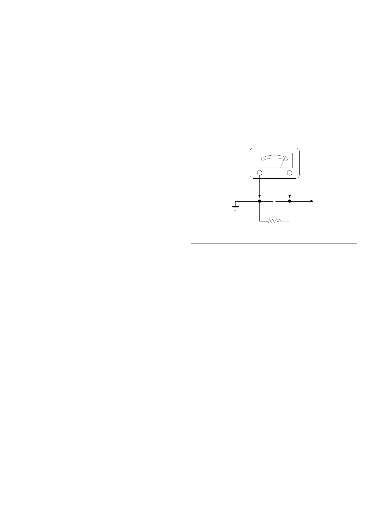
4) Before returning the set to the customer, always perform an AC leakage current check on the exposed metallic parts of the cabinet, such as antennas,
terminals, screw-heads, metal overlays, control shafts etc. to be sure the set
is safe to operate without danger of electrical shock. Plug the AC line cord
directly into a 120V AC outlet (do not use a line isolation transformer during
this check). Use an AC voltmeter having 5000 ohms per volt or more sensitivi-ty in the following manner.
Connect at 1500 ohm 10 watt resistor, paralleled by a 0.15 mfd. AC type
capacitor, between a known good earth ground (water pipe, conduit etc.)
and the exposed metallic parts, one at a time. Measure the AC voltage
across the combination of 1500 ohm resistor and 0.15 mfd capacitor. Voltage measured must not exceed 0.3 volts RMS. This corresponds to 0.2 millliamp. AC. Any value exceeding the limit constitutes a potential shock
hazard and must be corrected immediately.
AC VOLT METER
0.15uF
Good earth ground
such as d water
pipe, conduit, etc.
1500 OHM
10WATT
Place this probe
on each exposed
metallic part.
3. Product Safety Notice
Many electrical and mechanical parts in this chassis have special safety-related
characteristics. These characteristics are often passed unnoticed by a visual
inspection and the protection afforded by them cannot necessarily be obtained
by using replacement components rated for higher voltage, wattage, etc.
Replacement parts which have these special safety characteristics are identified in this manual and its supplements; electrical components having such features are identified by shading on the schematic diagram and the parts list.
Before replacing any of these components, read the parts list in this manual
carefully. The use of substitute replacement parts which do not have the same
safety characteristics as specified in the parts list may create X-ray radiation or
other hazards.
4. Service Notes
1) When replacing parts or circuit boards, clamp or bend the lead wires to terminals before soldering.
2) When replacing a high wattage resistor (metal oxide film resistor) in the circuit board, keep the resistor min 1/2 inch away form circuit board.
3) Keep wires away from high voltage or high temperature components.
DAEWOO ELECTRONICS CO., LTD.
C.P.OBOX8003 SEOUL, KOREA
Tel : 82-2-360-7798
Fax : 82-2-360-7877
E-mail : G7F00E@dwe.web.co.kr
Printed in Apr. 2000

Alignment Instructions
SVC v0
R BIAS
G BIAS
B BIAS
R DRIVE
G DRIVE
B DRIVE
V. CENTER
V. SIZE
H. CENTER
VCO
VCO FIN
VCO-L
VCO-L FIN
AGC
LED EAST
Pr
159
136
127
35
31
32
10
23
28
07
107
05
113
NO
44
01
ENTER SERVICE MODE
1. Select the Pr 91.
2. Adjust “ Sparpness “ to 0.
3. Enter the service mode
using the follow keys.
R G MENU.
2. SCREEN
1) Receive the Retma pattern and heat run over 15minutes.
2) Adjust the “R, G BIAS, R, G DRIVE” to 0, “B BIAS” to
127, “B DRIVE” to 32.
Adjust the screen volume that the Retma pattern reachs
the cut-off point.
3. WHITE BALANCE
1) Receive the Full white pattern and heat run over
15minutes.
2) Adjust the picture control at the point “X” value of white
balance instrument in 20cd/m
3) Enter the service mode.
4) Adjust “R BIAS, G BIAS” to x=288, y=301.
5) In order to exit the service mode power off the TV set and
power on.
6) Set the TV set to “Normal I” mode(20/21 inch) or set to
“Normal II” mode(14 inch)
7) Enter the service mode.
8) Adjust “R DRIVE, G DRIVE” to x=288, y=301.
9) Repeat above process until the white balance value to
x=288, y=301, X=20, x=288, y=301, X=200
(approximate) in 2) -8).
1. AFT
1) Set a signal Generator with
- RF FREQUENCY = 38.9MHz, 34.2MHz (L’)
- RF OUTPUT LEVEL = 80+/-5dBuV
- System = PAL for 38.9MHz.
SECAM-I for 43.2MHz.
2) Connect the Signal Generator RF Output
(PAL 38.9MHz) to P101 (Tuner IF Output).
There must be no signal input to the tuner.
3) Locate the cusor to “VCO” in Service Mode Menu,
then press the “Vol +” key and wait until the
“Please wait” disappear on the TV screen.
4) Connect the Signal Generator RF Output
(SECAM-L 34.2MHz) to P101 (Tuner IF Output).
5) Locate the cusor to “VCO-L” in Service Mode Menu,
then press the “Vol +” key and wait until the
“Please wait” disappear on the TV screen.
4. FOCUS
1) Apply a RETMA PATTERN signal.
2) Adjust the Focus Volume on FBT to obtain optimal
resolution.
5. AGC
1) Set a pattern Generator with
- RF LEVEL = 60dBuV
- 100% FULL COLOR BAR
2) Connect the Pattern Genetator RF Output to tuner
RF input.
3) Connect the probe of oscilloscope in AGC pin of tuner.
4) Adjust the AGC point to MAX - 1V.
( Simple Method )
1) Receive the pattern.
2) Locate the cusor in “AGC” and adjust using the
“VOL +” or “VOL -” keys.
3) Adjust the point there is no noise in about 60dBuV and no
beat in about 90dBuV.

6. GEOMETRY
6.1 VERTICAL CENTER
1) Set the TV to “NORMAL I” mode.
2) Enter the service mode.
3) Locate the cusor at “V.CENTER” then press “VOL +”
or “VOL -” keys to adjust the center line with the
mechanical center marks of the CRT.
6.2 VERTICAL SIZE
* The VERTICAL CENTER adjustment has to be done in advance.
1) Receive the Retma pattern.
2) Set the TV to “NORMAL I” mode.
3) Enter the service mode.
4) Locate the cursor at “V.SIZE” then press “VOL +”
or “VOL -” keys to adjust the upper part of the picture.
6.3 HORIZONTAL CENTER
1) Apply a RETMA PATTERN signal.
2) Set the TV to “NORMAL I” mode.
3) Enter the service mode.
4) Locate the cursor at “H.CENTER” then press “VOL +”
or “VOL -” keys to adjust the picture centering.
if EEPROM(I702) has been changed;
- Option data has to be change and
- all alignment function has to be readjusted
* The initial state of adjustment are as follows;
- V-Center, V-Size, H-Center, R, G, B, AFT = Center ( )
- AGC =
* Service Remocon

Electrical Parts List
LOC PART CODE PART NAME PART DESCRIPTION
R
ZZ100 48B3740A01
ZZ110 PTACPWA627 ACCESSORY AS DTP-14C5TF
100 4850Q00910 BATTERY R03/NN
M821 4858213800 BAG INSTRUCTION L.D.P.E T0.05X250X400
ZZ120 PTBCSHA627 COVER BACK AS DTP-14C5TF
R
M211 4852151401 COVER BACK HIPS BK
M541 4855415800 SPEC PLATE 150ART P/E FILM (C/TV)
ZZ130 PTPKCPA627 PACKING AS DTP-14C5TF
M801 4858038700 BOX CARTON SW-2 DTQ-1463FW
M811 4858189600 PAD EPS 14V5
M821 4858210600 BAG P.E
ZZ131 48519A4710 CRT GROUND NET 1401S-1015-1P
ZZ132 58G0000084 COIL DEGAUSSING DC-1450
ZZ140 PTCACAA627 CABINET AS DTP-14C5TF
R
CRT1 PTRTPWA605 CRT AS PAL 14" ITC CRT AS
V01 58D0000082 COIL DY ODY-M1489
V02 48A96R004- RUBBER WEDGE HMR 28 SR (|0X54)
V03 4850PM001- MAGNET CP NY-225 (MINI NECK)
V04 2TC26019BE TAPE CLOTH 19X30 BEIGE
V05 2224050026 BOND SILICON RTV 122 CARTRIDGE
V06 2233030001 PAINT LOCK 3B-1401B
V901 48A96414P4 CRT BARE A34JLL90X(K)
M193 4851937902 BUTTON CTRL 4942102+5537501
R
M321 4853214800 BRKT FR HIPS BK
R
M491B 4854942103 BUTTON ABS BK
M561 4855621401 MARK BRAND ABS BK
M681 4856812001 TIE CABLE NYLON66 DA100
SP01A 7178301011 SCREW TAPPTITE TT2 WAS 3X10 MFZN
R
ZZ200 PTFMSJA627 MASK FRONT AS DTP-14C5TF
M201 4852069901 MASK FRONT HIPS BK
ZZ210 PTSPPWA627 SPEAKER AS DTP-14C5TF
P601A 4850703S50 CONNECTOR
R
SP01 4858314010 SPEAKER SP-5070F01 3W 8 OHM
R
ZZ290 PTMPMSA627
C101 CEXF1H109V C ELECTRO 50V RSS 1MF (5X11) TP
C102 CEXF1H479V C ELECTRO 50V RSS 4.7MF (5X11) TP
C103 CEXF1C222V C ELECTRO
C301 CEXF1V471C C ELECTRO
C302 CCXB3A471K C CERA 1KV B 470PF K (T)
C303 CEXF1E102C C ELECTRO
C304 CEXF1H220V C ELECTRO 50V RSS 22MF (5X11) TP
C305 CMXE2A473J C MYLAR 100V PU 0.047MF J
C306 CEXF1V101C C ELECTRO
C307 CMXB1H224J C MYLAR 50V EU 0.22MF J (TP)
C313 CEXF1H109V C ELECTRO 50V RSS 1MF (5X11) TP
C401 CMYE2D364J C MYLAR 200V PU 0.36MF J
C402 CEXF2C109V C ELECTRO 160V RSS 1MF (6.3X11) TP
C404 CMYH3C692J C MYLAR 1.6KV BUP 6900PF J
C406 CCXB2H102K C CERA
TRANSMITTER
REMOCON
PCB MAIN MANUAL
AS
R-40A01
L.D.P.E
T0.03X1000X900
YH02503+35098+ULW=200
DTP-14C5TF
16V RSS 2200MF
(13X25) TP
35V RUS 470MF
(10X20) TP
25V RUS 1000MF
(13X20) TP
35V RUS 100MF
(8X11.5) TP
500V B 1000PF K
(TAPPING)
is a recommendable part for stock.
®
is safety component, so it must be used the same component.
LOC PART CODE PART NAME PART DESCRIPTION
C410 CMXM2A104J C MYLAR 100V 0.1MF J (TP)
C411 CMYN1J105K C MYLAR (MKT) 63V 1MF K (7.5MM)
C420 CEXF1C470V C ELECTRO 16V RSS 47MF (5X11) TP
C421 CEXF2E330V C ELECTRO 250V RSS 33MF (13X25) TP
C501 CEXF1H478V C ELECTRO 50V RSS 0.47MF (5X11) TP
C502 CEXF1H109V C ELECTRO 50V RSS 1MF (5X11) TP
C503 CEXF1C470V C ELECTRO 16V RSS 47MF (5X11) TP
C504 CEXD1H229F C ELECTRO 50V RND 2.2MF (5X11) TP
C506 CEXD1H229F C ELECTRO 50V RND 2.2MF (5X11) TP
C507 CEXF1C101V C ELECTRO
16V RSS 100MF
(6.3X11) TP
C511 CEXF1C470V C ELECTRO 16V RSS 47MF (5X11) TP
C512 CEXF1H109V C ELECTRO 50V RSS 1MF (5X11) TP
C513~7 CEXF1H100V C ELECTRO 50V RSS 10MF (5X11) TP
C520 CEXF1C470V C ELECTRO 16V RSS 47MF (5X11) TP
C522 CEXF1C470V C ELECTRO 16V RSS 47MF (5X11) TP
C523 CEXF1H109V C ELECTRO 50V RSS 1MF (5X11) TP
C524 CEXF1H109V C ELECTRO 50V RSS 1MF (5X11) TP
C601 CEXF1C101V C ELECTRO
16V RSS 100MF
(6.3X11) TP
C602 CEXF1H108A C ELECTRO 50V RSM 0.1MF 4X7
C606 CEXF1C101V C ELECTRO
16V RSS 100MF
(6.3X11) TP
C611 CEXF1C470V C ELECTRO 16V RSS 47MF (5X11) TP
C620 CEXF1H100V C ELECTRO 50V RSS 10MF (5X11) TP
C702 CEXF1H109V C ELECTRO 50V RSS 1MF (5X11) TP
C703 CEXF1C470V C ELECTRO 16V RSS 47MF (5X11) TP
C704 CEXF1C102V C ELECTRO
16V RSS 1000MF
(10X20) TP
C706 CEXF1H478V C ELECTRO 50V RSS 0.47MF (5X11) TP
C801 CL1JB3474K C LINE ACROSS
AC250V 0.47MF U/C/
SNDF/SV
C803 CCXF3A472Z C CERA 1KV F 4700PF Z (T)
C804 CCXF3A472Z C CERA 1KV F 4700PF Z (T)
C805 CEYN2G181P C ELECTRO 400V LHS 180MF (25X35)
C807 CMYU3C222J C MYLAR 1.6KV BCP 2200PF J
C809 CH1HFE102M C CERA AC 4.0KV 1000PF E DG
C812 CH1HFE102M C CERA AC 4.0KV 1000PF E DG
C814 CCYR3A471K C CERA
C815 CEXF2C101V C ELECTRO
1KV R 470PF K 125
DE0705
160V RSS 100MF
(16X25) TP
C816 CCXB3A471K C CERA 1KV B 470PF K (T)
C818 CEXF2C101C C ELECTRO
C819 CEXF2A100V C ELECTRO
C820 CEXF1E102V C ELECTRO
C822 CEXF1C101V C ELECTRO
160V RUS 100MF
(16X25) TP
100V RSS 10MF
(6.3X11) TP
25V RSS 1000MF
(13X20) TP
16V RSS 100MF
(6.3X11) TP
C823 CCXB3A471K C CERA 1KV B 470PF K (T)
C824 CCXB3A471K C CERA 1KV B 470PF K (T)
C825 CEXF1H220V C ELECTRO 50V RSS 22MF (5X11) TP
C826 CEXF1H479V C ELECTRO 50V RSS 4.7MF (5X11) TP
C827 CEXF1C222V C ELECTRO
16V RSS 2200MF
(13X25) TP
LOC PART CODE PART NAME PART DESCRIPTION
C828 CEXF1C101V C ELECTRO
C829 CEXF1H100V C ELECTRO 50V RSS 10MF (5X11) TP
C830 CEXF1C471V C ELECTRO
C841 CCXF1H103Z C CERA 50V F 0.01MF Z (TAPPING)
C842 CCXB3A102K C CERA 1KV B 1000PF K (TAPPING)
C850 CEXF1C470V C ELECTRO 16V RSS 47MF (5X11) TP
C902 CMXL2E104K C MYLAR 250V MEU 0.1MF K
C905 CMXL2E104K C MYLAR 250V MEU 0.1MF K
C906 CBXB3D102K C CERA SEMI 2KV BL(N) 1000PF K (T)
CC102 HCFK104ZCA C CHIP CERA 50V Y5V 0.1MF Z 2012
CC103 HCQK101JCA C CHIP CERA 50V CH 100PF J 2012
CC104 HCQK101JCA C CHIP CERA 50V CH 100PF J 2012
CC105 HCQK102JCA C CHIP CERA 50V CH 1000PF J 2012
CC108 HCFK104ZCA C CHIP CERA 50V Y5V 0.1MF Z 2012
CC109 HCFK104ZCA C CHIP CERA 50V Y5V 0.1MF Z 2012
CC118 HCBK104KCA C CHIP CERA 50V X7R 0.1MF K 2012
CC412 HCQK160JCA C CHIP CERA 50V CH 16PF J 2012
CC501 HCQK101JCA C CHIP CERA 50V CH 100PF J 2012
CC502 HCFK103ZCA C CHIP CERA 50V Y5V 0.01MF Z 2012
CC504 HCFK104ZCA C CHIP CERA 50V Y5V 0.1MF Z 2012
CC505 HCBK222KCA C CHIP CERA 50V X7R 2200PF K 2012
CC506 HCQK102JCA C CHIP CERA 50V CH 1000PF J 2012
CC508 HCBK472KCA C CHIP CERA 50V X7R 4700PF K 2012
CC509~12 HCFK104ZCA C CHIP CERA 50V Y5V 0.1MF Z 2012
CC515~7 HCFK104ZCA C CHIP CERA 50V Y5V 0.1MF Z 2012
CC518 HCBK222KCA C CHIP CERA 50V X7R 2200PF K 2012
CC519 HCFK334ZCA C CHIP CERA 50V Y5V 0.33MF Z 2012
CC520 HCFK104ZCA C CHIP CERA 50V Y5V 0.1MF Z 2012
CC521 HCBK472KCA C CHIP CERA 50V X7R 4700PF K 2012
CC522~4 HCQK102JCA C CHIP CERA 50V CH 1000PF J 2012
CC526 HCBK223KCA C CHIP CERA 50V X7R 0.022MF K 2012
CC533 HCFK104ZCA C CHIP CERA 50V Y5V 0.1MF Z 2012
CC534 HCQK300JCA C CHIP CERA 50V CH 30PF J 2012
CC535 HCQK300JCA C CHIP CERA 50V CH 30PF J 2012
CC536 HCQK300JCA C CHIP CERA 50V CH 30PF J 2012
CC602~4 HCQK102JCA C CHIP CERA 50V CH 1000PF J 2012
CC605 HCQK471JCA C CHIP CERA 50V CH 470PF J 2012
CC606 HCQK471JCA C CHIP CERA 50V CH 470PF J 2012
CC610 HCQK181JCA C CHIP CERA 50V CH 180PF J 2012
CC612 HCFK104ZCA C CHIP CERA 50V Y5V 0.1MF Z 2012
CC613 HCFK103ZCA C CHIP CERA 50V Y5V 0.01MF Z 2012
CC701 HCFK104ZCA C CHIP CERA 50V Y5V 0.1MF Z 2012
CC702 HCQK820JCA C CHIP CERA 50V CH 82PF J 2012
CC705 HCBK472KCA C CHIP CERA 50V X7R 4700PF K 2012
CC707 HCQK820JCA C CHIP CERA 50V CH 82PF J 2012
CC708 HCBK472KCA C CHIP CERA 50V X7R 4700PF K 2012
CC709 HCQK220JCA C CHIP CERA 50V CH 22PF J 2012
CC713 HCBK222KCA C CHIP CERA 50V X7R 2200PF K 2012
CC722 HCQK102JCA C CHIP CERA 50V CH 1000PF J 2012
CC723 HCQK220JCA C CHIP CERA 50V CH 22PF J 2012
CC801 HCFK104ZCA C CHIP CERA 50V Y5V 0.1MF Z 2012
CC830 HCFK104ZCA C CHIP CERA 50V Y5V 0.1MF Z 2012
D101 D1N4148--- DIODE 1N4148 (TAPPING)
D103 D1SS85TA-- DIODE 1SS85TA
D105 DUZ33B---- DIODE ZENER UZ-33B
D106 D1N4148--- DIODE 1N4148 (TAPPING)
16V RSS 100MF
(6.3X11) TP
16V RSS 470MF
(10X12.5)TP
LOC PART CODE PART NAME PART DESCRIPTION
D107 DUZ5R1B--- DIODE ZENER UZ-5.1B UNIZON
D301,3 D1N4937G-- DIODE 1N4937G (TAPPING)
D402~3 D1N4937G-- DIODE 1N4937G (TAPPING)
D404 DDG3------ DIODE DG3
D410 DUZ5R1B--- DIODE ZENER UZ-5.1B UNIZON
D450 D1N4148--- DIODE 1N4148 (TAPPING)
D452 D1N4148--- DIODE 1N4148 (TAPPING)
D501~7 DUZ5R6BM-- DIODE ZENER UZ-5.6BM(TAPPING)
D508 D1N4148--- DIODE 1N4148 (TAPPING)
D509 D1N4148--- DIODE 1N4148 (TAPPING)
D510 DUZ5R1B--- DIODE ZENER UZ-5.1B UNIZON
D512~4 D1N4148--- DIODE 1N4148 (TAPPING)
D602 DUZ5R6BM-- DIODE ZENER UZ-5.6BM(TAPPING)
D610 D1N4148--- DIODE 1N4148 (TAPPING)
D620 D1N4148--- DIODE 1N4148 (TAPPING)
D701 DUZ3R9B--- DIODE ZENER UZ-3.9B
D704 85801065GY WIRE COPPER
AWG22 1/0.65 TIN
COATING
D706 DLH2PR---- LED BLOCK LH-2P-R
D720 D1N4148--- DIODE 1N4148 (TAPPING)
D806 DRGP30J--- DIODE RGP30J
D808,10,
D1N4936GP- DIODE 1N4936GP (TAPPING)
12
D816 DUZ3R9B--- DIODE ZENER UZ-3.9B
D820 D1N4148--- DIODE 1N4148 (TAPPING)
D835 DR2M------ DIODE ZENER R2M
D837~40 DLT2A05G-- DIODE LT2A05G (TP)
F801 5FSCB4022R FUSE CERA
SEMKO F4AH 4A 250V
MF51
F801A 4857415001 CLIP FUSE PFC5000-0702
F801B 4857415001 CLIP FUSE PFC5000-0702
I301 PTA2SW7104 HEAT SINK ASS`Y 1TDA1771-- + 7174301011
I301 1TDA1771-- IC VERTICAL TDA1771
R
I301A 4857027104 HEAT SINK SPCC T1.0+SN
I301B 7174301011 SCREW TAPPTITE TT2 RND 3X10 MFZN
R
I501 1STV2238DQ IC CHIP VIDEO STV2238D
R
I601 1TDA7267A- IC AMP TDA7267A
R
I701 1DW195DE1Q IC MICOM DW92195B7T-DE1(ERP)
R
I702 1AT24C16PC IC AT24C16-10PC
R
I703 1KA7805--- IC REGULATOR KA7805
I704 1KRT30---- IC PREAMP KRT30
R
R
I802 4850M04710 MODULE POWER DPM001T1A
I805 PTA2SW6904 HEAT SINK ASS`Y 1STV8131-- + 7174301011
I805 1STV8131-- IC REGULATOR STV8131
R
I805A 4857026904 HEAT SINK AL EX
I805B 7174301011 SCREW TAPPTITE TT2 RND 3X10 MFZN
I901 PTB3SW1100 HEAT SINK ASS`Y 1TDA6103Q- + 7174301011
R
I901 1TDA6103Q- IC VIDEO TDA6103Q
I901A 4857031100 HEAT SINK A1050P-H24 T2.0
I901B 7174301011 SCREW TAPPTITE TT2 RND 3X10 MFZN
J046 RD-4Z101J- R CARBON FILM 1/4 100 OHM J
JC001~6 HRFT000-CA R CHIP 1/10 0 OHM 2012
JC008~9 HRFT000-CA R CHIP 1/10 0 OHM 2012
JC011~20 HRFT000-CA R CHIP 1/10 0 OHM 2012
JC022 HRFT000-CA R CHIP 1/10 0 OHM 2012
JC024~5 HRFT000-CA R CHIP 1/10 0 OHM 2012
JS02 4859109950 JACK PIN BOARD PH-JB-9710A
L101 58N0000044 COIL VCO TRF-V010
L301 5CPZ100K04 COIL PEAKING 10UH 10.5MM K (LAL04TB)
L511 5CPZ100K02 COIL PEAKING 10UH K (AXIAL 3.5MM)
L601 5CPZ109M02 COIL PEAKING 1UH M (AXIAL 3.5MM)
L602 5CPZ109M02 COIL PEAKING 1UH M (AXIAL 3.5MM)
LOC PART CODE PART NAME PART DESCRIPTION
L603 85801065GY WIRE COPPER
AWG22 1/0.65 TIN
COATING
L604 5CPZ109M02 COIL PEAKING 1UH M (AXIAL 3.5MM)
L606 85801065GY WIRE COPPER
AWG22 1/0.65 TIN
COATING
L701 5CPZ100K02 COIL PEAKING 10UH K (AXIAL 3.5MM)
L702 5CPZ569K02 COIL PEAKING 5.6UH K (AXIAL 3.5MM)
L800 58Q0000093 COIL DELAY LINE RS208
L801 5PLF24A3-- FILTER LINE LF-24A3
L802 5MC0000100 COIL BEAD HC-3550
L803 5MC0000100 COIL BEAD HC-3550
L805 58C4500079 COIL CHOKE L-45
L806 5CPZ390K04 COIL PEAKING 39UH 10.5MM K (LAL04TB)
M681 4856812001 TIE CABLE NYLON66 DA100
M721 4857235402 SHIELD CASE SPTH-C T0.25
P401 4859240020 CONN WAFER YFW500-05
P601 485923162S CONN WAFER YW025-03 (STICK)
P801 4859287320 CONN WAFER MKS2822-6-10-202
P802 4859242220 CONN WAFER YFW800-02
P901 4850709N02 CONNECTOR
PA801 4859906210 CORD POWER AS 6-L0+H03VVH2=2200
R
YBNH250-
09YBNT025+ULW=300
Q105 TKTC3198Y- TR KTC3198Y
Q401 TKTC3207-- TR KTC3207 (TP)
R
Q402 T2SD2499-- TR 2SD2499
Q501 TKTC3198Y- TR KTC3198Y
Q502 TKTC3198Y- TR KTC3198Y
Q503 TKTA1266Y- TR KTA1266Y (TP)
Q505 TKTA1266Y- TR KTA1266Y (TP)
Q506 TKTC3198Y- TR KTC3198Y
Q601 TKTC3198Y- TR KTC3198Y
Q620 TKTA1266Y- TR KTA1266Y (TP)
Q701 TKTA1266Y- TR KTA1266Y (TP)
Q702 TKTC3198Y- TR KTC3198Y
Q703 TKTC3198Y- TR KTC3198Y
Q704 TKTC3198Y- TR KTC3198Y
Q705 TKTC3198Y- TR KTC3198Y
Q710 TKTC3198Y- TR KTC3198Y
Q801 PTR2SW4500 HEAT SINK ASS`Y T2SK2671-- + 7174300811
R
Q801 T2SK2671-- FET 2SK2671
Q801A 4857024500 HEAT SINK AL EX B/K
Q801B 7174300811 SCREW TAPPTITE TT2 RND 3X8 MFZN
R
Q802 TKSA1013Y- TR KSA1013Y (TP)
R101 RD-4Z242J- R CARBON FILM 1/4 2.4K OHM J
R109 RD-4Z183J- R CARBON FILM 1/4 18K OHM J
R110 RD-4Z102J- R CARBON FILM 1/4 1K OHM J
R111 RD-4Z101J- R CARBON FILM 1/4 100 OHM J
R120 RD-4Z101J- R CARBON FILM 1/4 100 OHM J
R301 RD-2Z249J- R CARBON FILM 1/2 2.4 OHM J
R302 RN02B229JS R METAL FILM 2W 2.2 OHM J SMALL
R303 RN02B271JS R METAL FILM 2W 270 OHM J SMALL
R307 RN02B181JS R METAL FILM 2W 180 OHM J SMALL
R308 RN02B181JS R METAL FILM 2W 180 OHM J SMALL
R309 RN02B181JS R METAL FILM 2W 180 OHM J SMALL
R310 RN02B181JS R METAL FILM 2W 180 OHM J SMALL
R402 RS02Z103JS R M-OXIDE FILM 2W 10K OHM J SMALL
R403 RS01Z439J- R M-OXIDE FILM 1W 4.3 OHM J
R406 RD-2Z472J- R CARBON FILM 1/2 4.7K OHM J
R407 RD-4Z102J- R CARBON FILM 1/4 1K OHM J
R408 RD-4Z102J- R CARBON FILM 1/4 1K OHM J
R409 RD-4Z561J- R CARBON FILM 1/4 560 OHM J
R410 RN01B132JS R METAL FILM 1W 1.3K OHM J SMALL
LOC PART CODE PART NAME PART DESCRIPTION
R501 RD-4Z101J- R CARBON FILM 1/4 100 OHM J
R502 RD-4Z101J- R CARBON FILM 1/4 100 OHM J
R503 RN01B300JS R METAL FILM 1W 30 OHM J SMALL
R512 RD-4Z750J- R CARBON FILM 1/4 75 OHM J
R521 RD-4Z101J- R CARBON FILM 1/4 100 OHM J
R525 RD-4Z104J- R CARBON FILM 1/4 100K OHM J
R526 RD-4Z102J- R CARBON FILM 1/4 1K OHM J
R532 RD-4Z101J- R CARBON FILM 1/4 100 OHM J
R601 RD-2Z102J- R CARBON FILM 1/2 1K OHM J
R602 RD-4Z511J- R CARBON FILM 1/4 510 OHM J
R611 RD-4Z362J- R CARBON FILM 1/4 3.6K OHM J
R715 RD-4Z102J- R CARBON FILM 1/4 1K OHM J
R723 RD-4Z332J- R CARBON FILM 1/4 3.3K OHM J
R735 RD-4Z103J- R CARBON FILM 1/4 10K OHM J
R736 RD-4Z224J- R CARBON FILM 1/4 220K OHM J
R753 RD-4Z473J- R CARBON FILM 1/4 47K OHM J
R801 DEC140M290 POSISTOR ECPCC140M290
R802 RX07C339JF R CEMENT 7W 3.3 OHM J 15MM 4P
R803 RD-4Z514J- R CARBON FILM 1/4 510K OHM J
R804 RD-4Z514J- R CARBON FILM 1/4 510K OHM J
R805 85801065GY WIRE COPPER
AWG22 1/0.65 TIN
COATING
R806 RD-4Z363J- R CARBON FILM 1/4 36K OHM J
R808 RS02Z828JS R M-OXIDE FILM 2W 0.82 OHM J SMALL
R809 RD-4Z103J- R CARBON FILM 1/4 10K OHM J
R810 RD-4Z333J- R CARBON FILM 1/4 33K OHM J
R812 RC-2Z825KP R CARBON COMP 1/2 8.2M OHM K
R819 RS02Z278JS R M-OXIDE FILM 2W 0.27 OHM J SMALL
R823 RD-4Z101J- R CARBON FILM 1/4 100 OHM J
R824 RD-4Z101J- R CARBON FILM 1/4 100 OHM J
R834 RD-4Z392J- R CARBON FILM 1/4 3.9K OHM J
R850 RN02B180JS R METAL FILM 2W 18 OHM J SMALL
R890 RC-2Z335KP R CARBON COMP 1/2 3.3M OHM K
R901~3 RN01B124JS R METAL FILM 1W 120K OHM J SMALL
R910~2 RD-2Z152J- R CARBON FILM 1/2 1.5K OHM J
RC106 HRFT682JCA R CHIP 1/10 6.8K OHM J 2012
RC107 HRFT473JCA R CHIP 1/10 47K OHM J 2012
RC111 HRFT511JCA R CHIP 1/10 510 OHM J 2012
RC114 HRFT432JCA R CHIP 1/10 4.3K OHM J 2012
RC115 HRFT102JCA R CHIP 1/10 1K OHM J 2012
RC301 HRFT361JCA R CHIP 1/10 360 OHM J 2012
RC302 HRFT202JCA R CHIP 1/10 2K OHM J 2012
RC303 HRFT562JCA R CHIP 1/10 5.6K OHM J 2012
RC304 HRFT272JCA R CHIP 1/10 2.7K OHM J 2012
RC306 HRFT472JCA R CHIP 1/10 4.7K OHM J 2012
RC307 HRFT562JCA R CHIP 1/10 5.6K OHM J 2012
RC308 HRFT332JCA R CHIP 1/10 3.3K OHM J 2012
RC309 HRFT154JCA R CHIP 1/10 150K OHM J 2012
RC310 HRFT103JCA R CHIP 1/10 10K OHM J 2012
RC313 HRFT224JCA R CHIP 1/10 220K OHM J 2012
RC404 HRFT561JCA R CHIP 1/10 560 OHM J 2012
RC405 HRFT362JCA R CHIP 1/10 3.6K OHM J 2012
RC408 HRFT103JCA R CHIP 1/10 10K OHM J 2012
RC419 HRFT152JCA R CHIP 1/10 1.5K OHM J 2012
RC420 HRFT394JCA R CHIP 1/10 390K OHM J 2012
RC501 HRFT750JCA R CHIP 1/10 75 OHM J 2012
RC503~5 HRFT750JCA R CHIP 1/10 75 OHM J 2012
RC506 HRFT101JCA R CHIP 1/10 100 OHM J 2012
RC507 HRFT103JCA R CHIP 1/10 10K OHM J 2012
RC508 HRFT103JCA R CHIP 1/10 10K OHM J 2012
RC509 HRFT102JCA R CHIP 1/10 1K OHM J 2012
RC510 HRFT102JCA R CHIP 1/10 1K OHM J 2012

LOC PART CODE PART NAME PART DESCRIPTION
RC511 HRFT470JCA R CHIP 1/10 47 OHM J 2012
RC512 HRFT223JCA R CHIP 1/10 22K OHM J 2012
RC513 HRFT103JCA R CHIP 1/10 10K OHM J 2012
RC514 HRFT151JCA R CHIP 1/10 150 OHM J 2012
RC515 HRFT000-CA R CHIP 1/10 0 OHM 2012
RC516 HRFT102JCA R CHIP 1/10 1K OHM J 2012
RC517 HRFT102JCA R CHIP 1/10 1K OHM J 2012
RC518 HRFT101JCA R CHIP 1/10 100 OHM J 2012
RC519 HRFT101JCA R CHIP 1/10 100 OHM J 2012
RC520 HRFT103JCA R CHIP 1/10 10K OHM J 2012
RC521 HRFT363JCA R CHIP 1/10 36K OHM J 2012
RC522 HRFT222JCA R CHIP 1/10 2.2K OHM J 2012
RC523 HRFT822JCA R CHIP 1/10 8.2K OHM J 2012
RC524 HRFT103JCA R CHIP 1/10 10K OHM J 2012
RC525 HRFT153JCA R CHIP 1/10 15K OHM J 2012
RC526 HRFT273JCA R CHIP 1/10 27K OHM J 2012
RC527 HRFT473JCA R CHIP 1/10 47K OHM J 2012
RC528 HRFT221JCA R CHIP 1/10 220 OHM J 2012
RC529~31 HRFT271JCA R CHIP 1/10 270 OHM J 2012
RC532 HRFT273JCA R CHIP 1/10 27K OHM J 2012
RC534 HRFT334JCA R CHIP 1/10 330K OHM J 2012
RC535 HRFT184JCA R CHIP 1/10 180K OHM J 2012
RC537 HRFT103JCA R CHIP 1/10 10K OHM J 2012
RC538 HRFT223JCA R CHIP 1/10 22K OHM J 2012
RC539 HRFT122JCA R CHIP 1/10 1.2K OHM J 2012
RC541~3 HRFT222JCA R CHIP 1/10 2.2K OHM J 2012
RC553 HRFT102JCA R CHIP 1/10 1K OHM J 2012
RC555 HRFT101JCA R CHIP 1/10 100 OHM J 2012
RC560 HRFT472JCA R CHIP 1/10 4.7K OHM J 2012
RC605 HRFT153JCA R CHIP 1/10 15K OHM J 2012
RC606 HRFT153JCA R CHIP 1/10 15K OHM J 2012
RC610 HRFT102JCA R CHIP 1/10 1K OHM J 2012
RC611 HRFT152JCA R CHIP 1/10 1.5K OHM J 2012
RC620 HRFT101JCA R CHIP 1/10 100 OHM J 2012
RC621 HRFT104JCA R CHIP 1/10 100K OHM J 2012
RC623 HRFT512JCA R CHIP 1/10 5.1K OHM J 2012
RC630 HRFT102JCA R CHIP 1/10 1K OHM J 2012
RC702 HRFT102JCA R CHIP 1/10 1K OHM J 2012
RC703 HRFT102JCA R CHIP 1/10 1K OHM J 2012
RC704 HRFT562JCA R CHIP 1/10 5.6K OHM J 2012
RC705 HRFT153JCA R CHIP 1/10 15K OHM J 2012
RC706 HRFT562JCA R CHIP 1/10 5.6K OHM J 2012
RC707 HRFT101JCA R CHIP 1/10 100 OHM J 2012
RC708 HRFT102JCA R CHIP 1/10 1K OHM J 2012
RC709 HRFT222JCA R CHIP 1/10 2.2K OHM J 2012
RC710 HRFT222JCA R CHIP 1/10 2.2K OHM J 2012
RC711 HRFT222JCA R CHIP 1/10 2.2K OHM J 2012
RC712 HRFT101JCA R CHIP 1/10 100 OHM J 2012
RC713 HRFT101JCA R CHIP 1/10 100 OHM J 2012
RC714 HRFT102JCA R CHIP 1/10 1K OHM J 2012
RC715 HRFT152JCA R CHIP 1/10 1.5K OHM J 2012
RC716 HRFT392JCA R CHIP 1/10 3.9K OHM J 2012
RC717 HRFT153JCA R CHIP 1/10 15K OHM J 2012
RC719 HRFT332JCA R CHIP 1/10 3.3K OHM J 2012
RC720 HRFT271JCA R CHIP 1/10 270 OHM J 2012
RC721 HRFT102JCA R CHIP 1/10 1K OHM J 2012
RC722 HRFT332JCA R CHIP 1/10 3.3K OHM J 2012
RC723 HRFT624JCA R CHIP 1/10 620K OHM J 2012
RC725 HRFT471JCA R CHIP 1/10 470 OHM J 2012
LOC PART CODE PART NAME PART DESCRIPTION
RC726 HRFT103JCA R CHIP 1/10 10K OHM J 2012
RC727 HRFT103JCA R CHIP 1/10 10K OHM J 2012
RC729 HRFT101JCA R CHIP 1/10 100 OHM J 2012
RC730 HRFT332JCA R CHIP 1/10 3.3K OHM J 2012
RC731 HRFT100JCA R CHIP 1/10 10 OHM J 2012
RC732 HRFT000-CA R CHIP 1/10 0 OHM 2012
RC733 HRFT101JCA R CHIP 1/10 100 OHM J 2012
RC736 HRFT102JCA R CHIP 1/10 1K OHM J 2012
RC738 HRFT101JCA R CHIP 1/10 100 OHM J 2012
RC751 HRFT103JCA R CHIP 1/10 10K OHM J 2012
RC752 HRFT682JCA R CHIP 1/10 6.8K OHM J 2012
RC754 HRFT333JCA R CHIP 1/10 33K OHM J 2012
RC755 HRFT473JCA R CHIP 1/10 47K OHM J 2012
RC822 HRFT134JCA R CHIP 1/10 130K OHM J 2012
RC828 HRFT102JCA R CHIP 1/10 1K OHM J 2012
RC829 HRFT102JCA R CHIP 1/10 1K OHM J 2012
RC901 HRFT272JCA R CHIP 1/10 2.7K OHM J 2012
RC902 HRFT302JCA R CHIP 1/10 3K OHM J 2012
RC903 HRFT302JCA R CHIP 1/10 3K OHM J 2012
RC904 HRFT302JCA R CHIP 1/10 3K OHM J 2012
RC905~7 HRFT272JCA R CHIP 1/10 2.7K OHM J 2012
RLY1 5SC0101338 SW RELAY DQ5D1-O(M)/GJ-SS-105LM
SCT1 4859303430 SOCKET CRT PCS633A
SF101 5PG3962M-- FILTER SAW G 3962-M
SF102 5PK9650M-- FILTER SAW K9650M
SJ01 4859200401 SOCKET RGB YRS21-R1
SW701 5S50101090 SW TACT SKHV17910A
SW702 5S50101090 SW TACT SKHV17910A
SW703 5S50101090 SW TACT SKHV17910A
SW704 5S50101090 SW TACT SKHV17910A
SW705 5S50101090 SW TACT SKHV17910A
R
SW801 5S40101146 SW POWER PUSH SS-160-7-B
T401 50D10A3--- TRANS DRIVE TD-10A3
R
T402 50H0000202 FBT FUY20C001
T801 50M4042A5- TRANS SMPS TSM-4042A5
R
U101 4859719930 TUNER VARACTOR DT5-BF18D
W101 4851900130
X501 5XEX4R433B CRYSTAL QUARTZ
X502 5XEX3R579B CRYSTAL QUARTZ
GROUND TUNER
AS
DS-W1015-S
HC-49U 4.43361M 15PPM
TP
HC-49U 3.57954M 15PPM
TP
X701 5XEX4R000C CRYSTAL QUARTZ HC-49U 4.0000MHZ (TP)

Video
Audio
 Loading...