

Daewoo DP-A43D1D-AN, DP-A62D1D-LS, DP-A61D1D-LS, DP-A61D1S-BJ, DP-A61D1S-LS Service Manual
...
S/M No. : VD2113TET0
✔ Caution :
In this Manual, some parts can be changed for improving, their
performance without notice in the parts list. So, if you need the latest
parts information,please refer to PPL(Parts Price List) in Service
Information Center (http://svc.dwe.co.kr).
DAEWOO ELECTRONICS Corp.
Sep. 2003
http : //svc.dwe.co.kr
Service Manual
VE 2.0 DVD PLAYER
* Refer to the Model list of page 82.
MODEL : DP-A61D1D Series
DP-A61D1S Series
DP-A62D1D Series
DP-A62D1S Series
DP-A43D1D Series
DP-A64D2D Series
OPEN/CLOSE
PLAY
PAUSE/ STEP STOP PREV NEXT

EXTERNAL VIEWS.......................................................................................................2
1. FRONT VIEWS ......................................................................................................................................... 2
2. REAR VIEWS ............................................................................................................................................2
SPECIFICATIONS.........................................................................................................3
CIRCUIT DIAGRAM..................................................................................................................4
CIRCUIT OPERATIONAL DESCRIPTION .............................................................................16
TROUBLE SHOOTING...........................................................................................................35
WAVEFORMS .........................................................................................................................49
COMPONENTS LOCATION GUIDE ON PCB BOTTOM VIEW.............................................56
DISASSEMBLY.......................................................................................................................60
ELECTRICAL PARTSLIST.....................................................................................................71
1
CONTENTS
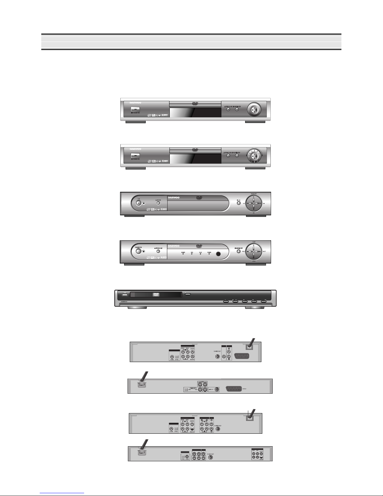
1. FORNT VIEWS
( Refer to the Model list of page
)
1)DQD-2113/DP-A61D1D Series(PANEL: 1, 2CH)
2)DQD-6113/DP-A61D1D Series(PANEL: 1, 5.1CH)
3)DVD-323/DVD-363/DP-A62D1D Series(PANEL:2, 2/5.1CH)
4)DVD-223/DVD-263/DP-A43D1D Series(PANEL:3, 2/5.1CH)
5)DVD-423/DVD-463/DP-A64D2D Series(PANEL:4, 2/5.1CH)
2. REAR VIEWS
1) PAL System Series
2) NTSC System Series
2
EXTERNAL VIEWS
EURO AV
DIGITAL AUDIO OUT
AUDIO OUT (5.1 CH)
AUDIO OUTVIDEO OUT
DIGITAL AUDIO OUT
AUDIO OUT (5.1 CH)
AUDIO OUT (2 CH)
VIDEO OUT
OPEN/CLOSE
PLAY
PAUSE/ STEP STOP PREV NEXT
65MM Model
65MM Model
65MM Model
65MM Model
43MM Model
65MM Model
43MM Model
65MM Model
43MM Model
DIGITAL AUDIO OUT
AUDIO OUT (5.1 CH)
AUDIO OUT (2 CH)
VIDEO OUT
82
3
SPECIFICATIONS
1. Prodcut features
- Over 500 resolution of horizontal frequency
- Dolby Digital decoding
- 5.1ch Analog signal output
- DTS output
- Screen zoom function
- Special playback function(slow playback/fast playback)
- NTSC Type : Component output(Y, Pb, Pr)
- PAL Type : RGB output
- Progressive SCAN (NTSC Only)
2. Specifications
Audio Dolby Digital Analog 5.1ch output and digital output
DTS Digital output
Convenience Screen zoom function OK
Special playback function OK
MP3 playback function OK
Connecting terminal Video terminal Composite terminal : 1 unit
Component terminal : 1 unit(NTSC only)
S-Video terminal : 1 unit
Audio terminal 2ch terminal : 1 unit
5.1ch terminal : 1 unit
Optical terminal : 1 unit
Coaxial terminal : 1 unit
Size 420mm x65mm x250.3mm (65MM Model)
420mm x42.8mm x257.2mm (43MM Model)
3. Playable Disc
Disc type Playable Restriction
DVD Possible Region 2 or Region ALL
Video CD Possible Version 1.0/1.1/2.0, SVCD
CD Possible PCM or dts
CD-G Possible Audio with graphic
CD-ROM Possible MP3/JPEG File
CD-R Possible Video-CD/CD/MP3/JPEG
CD-RW Possible Video-CD/CD/MP3/JPEG
DVD-R Possible DVD Video
DVD-RW Possible DVD Video
DVD+RW Possible DVD Video
DVD-ROM Impossible
DVD-RAM Impossible
Photo CD Impossible
4
CIRCUIT DIAGRAM
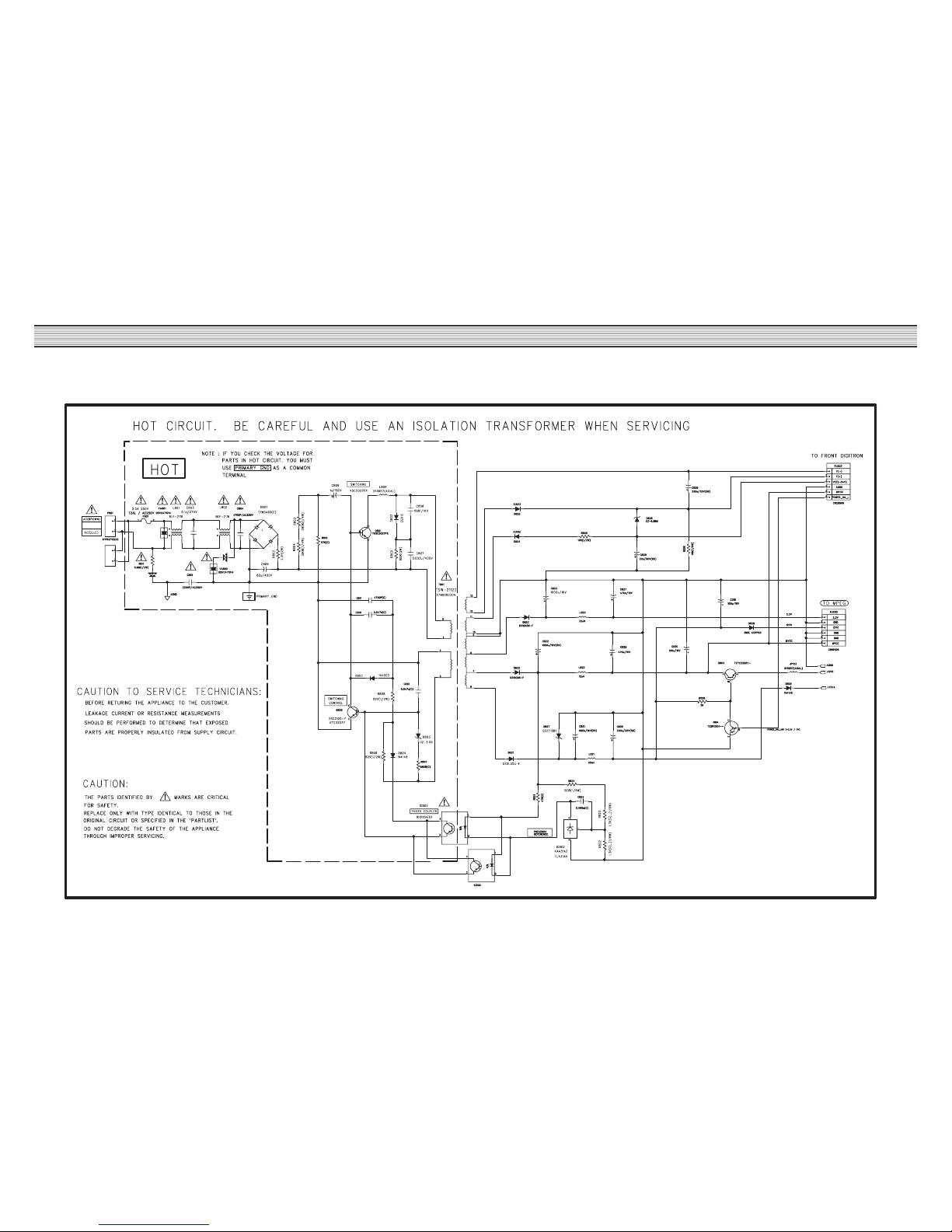
POWER SUPPLY SCHEMATIC DIAGRAM(DP-A62D1D-AN)/(65MM Mode)
5
CIRCUIT DIAGRAM
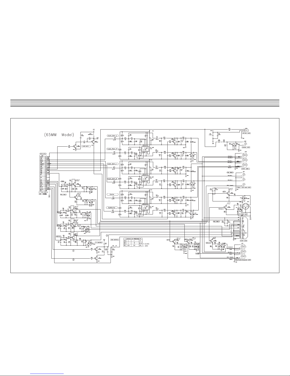
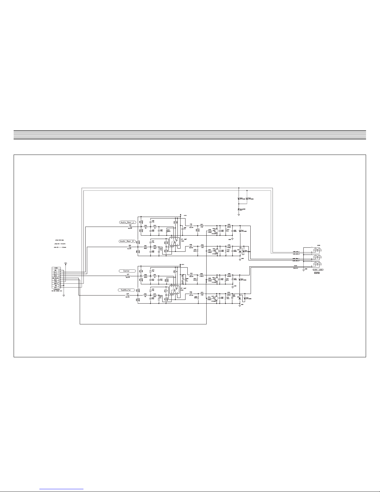
AUDIO (65MM)
6
CIRCUIT DIAGRAM
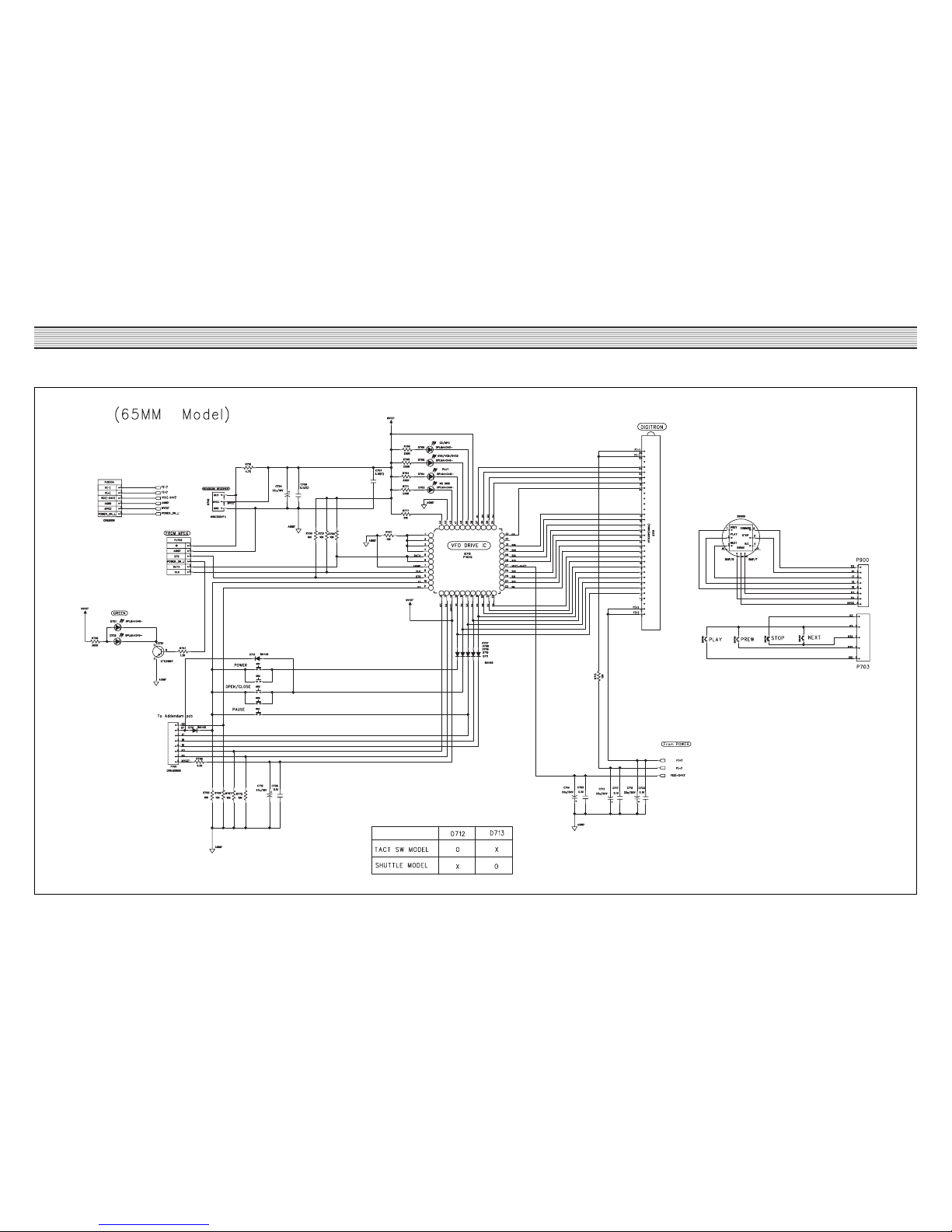
FRONT (VFD)-65MM
7
CIRCUIT DIAGRAM
AUDIO(43MM)
8
CIRCUIT DIAGRAM
AV(43MM)
9
CIRCUIT DIAGRAM
FRONT(43MM)

10
CIRCUIT DIAGRAM
DQL-1000(ALIM3351 MPEG IC)
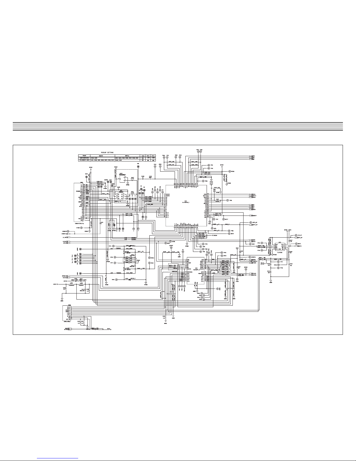
11
CIRCUIT DIAGRAM
DQL-1000(RF-MOTOR_DIRIVERS)
12
CIRCUIT DIAGRAM
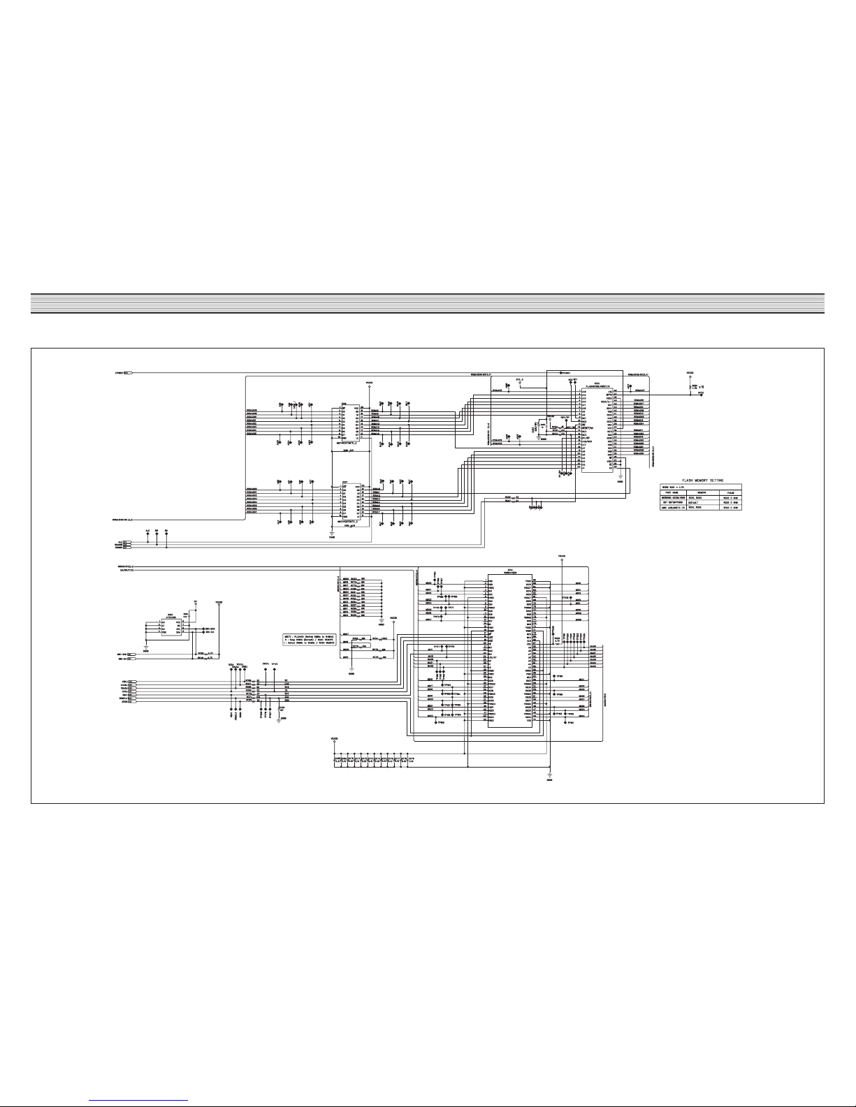
DQL-1000(FLASH, SDRAM)
13
CIRCUIT DIAGRAM
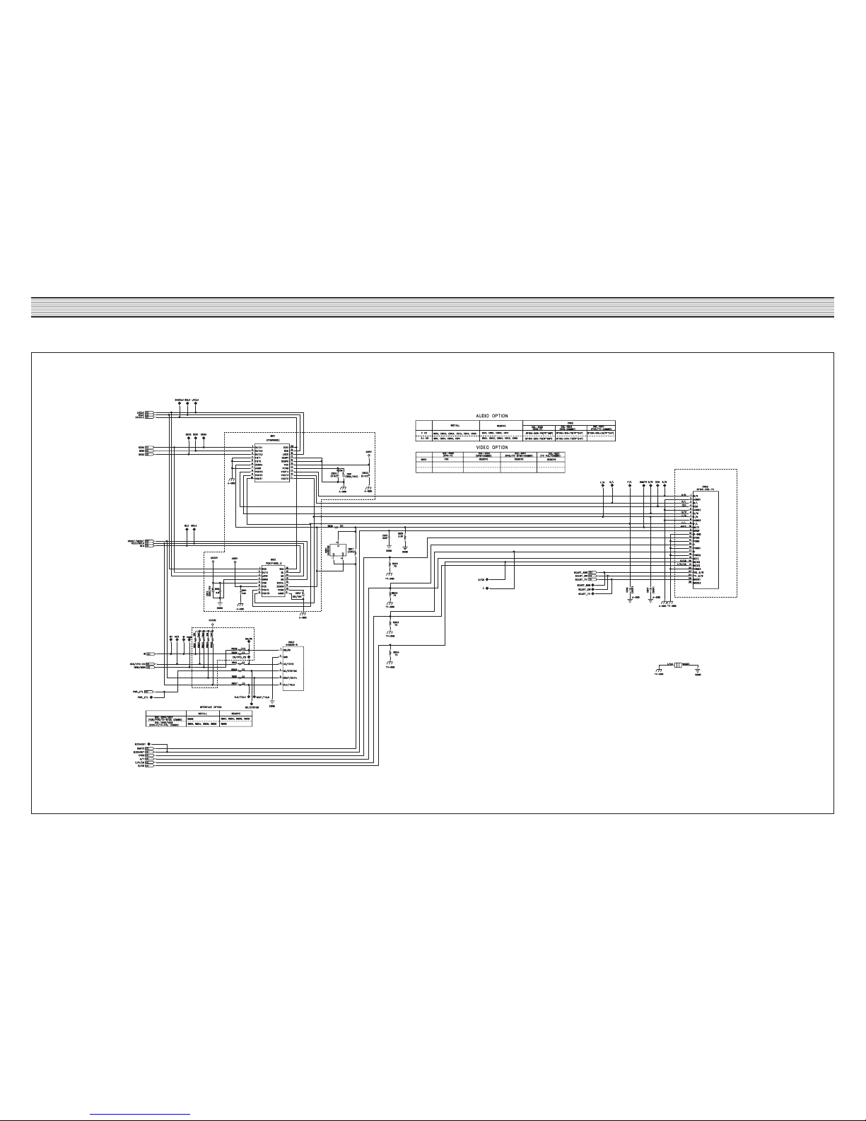
DQL-1000(AUDIO_DAC, VIDEO_CHANNEL)

14
CIRCUIT DIAGRAM
DQL-1000(SYSTEM_POWER)

15
CIRCUIT DIAGRAM
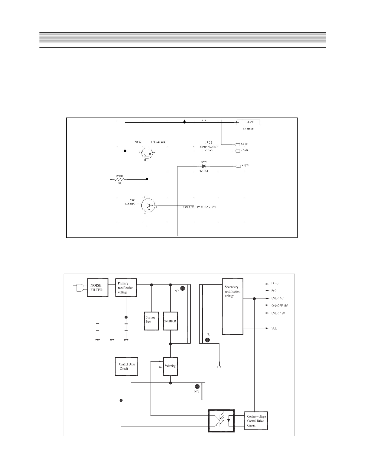
VE2.0 DVD-Player Series Block Diagram
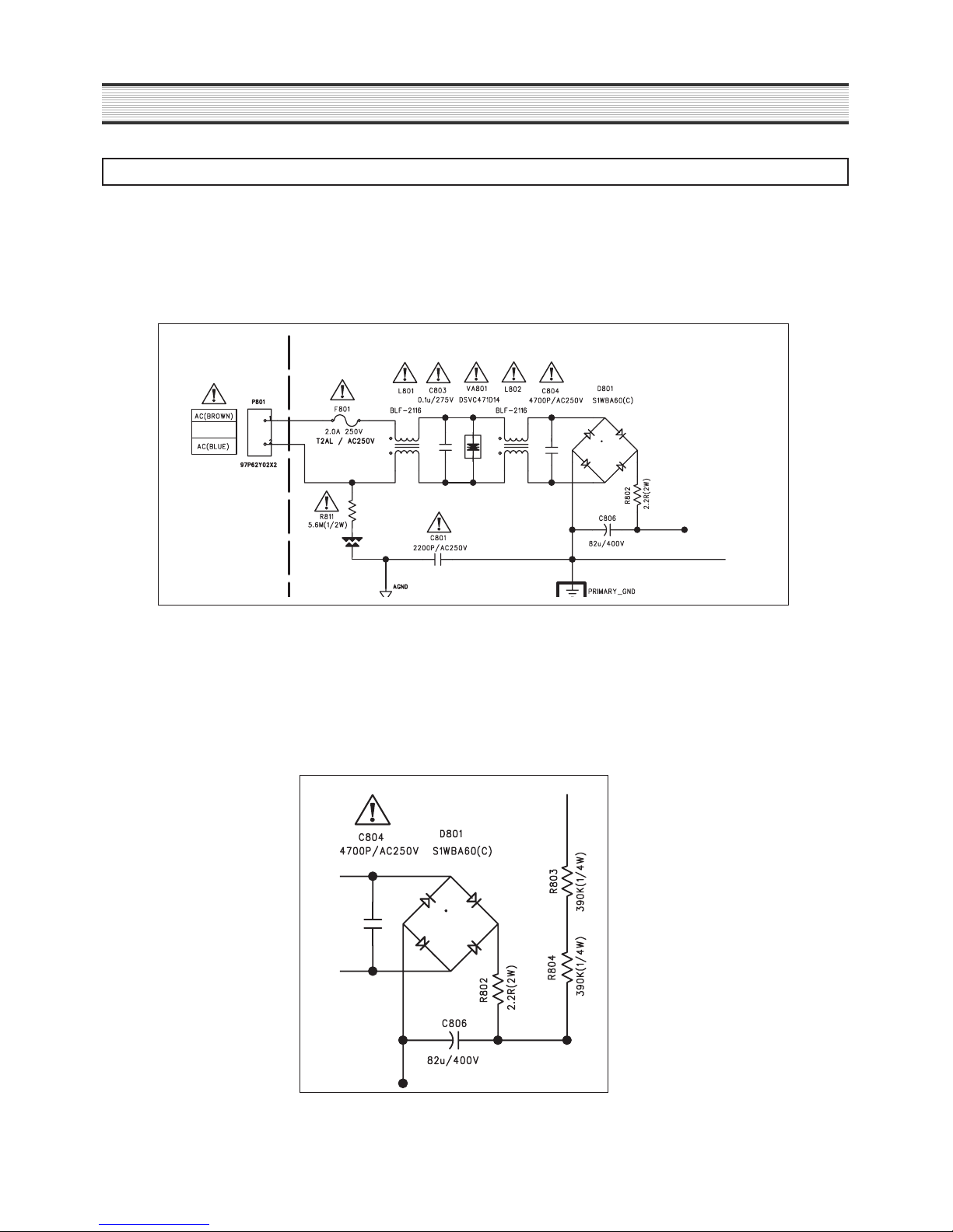
2) Primary rectification and smoothing circuit
AC voltage passed through AC lnlet is rectified to Brige Rectification Diode D801 and changes to DC voltage.
After that it smooths the Smoothing Condenser C806.
When C806 is charged at first, Resistor R802 intercepts voltage current and protects D801, F801.
Start Resistor R803, R804 supply Control IC VCC terminal with rectified DC voltage.
16
1. POWER SUPPLY OPERATION(220V)
1) AC input and EMI FILTER
AC inlet consists of fuse, Line Filter, X-Cap, Y-Cap, Varister. Line Filter(L801, L802), X-Cap(C803, C804), YCap(C801) belong to EMI Filter section. They decrease noise to get into and out of AC Line.
CIRCUIT OPERATIONAL DESCRIPTION
POWER SECTION
Picture 1. [AC Input section]
Picture 2 [Rectification, smoothing and starting circuit]
17
CIRCUIT OPERATIONAL DESCRIPTION
Picture
3 [
Snubber circuit
]
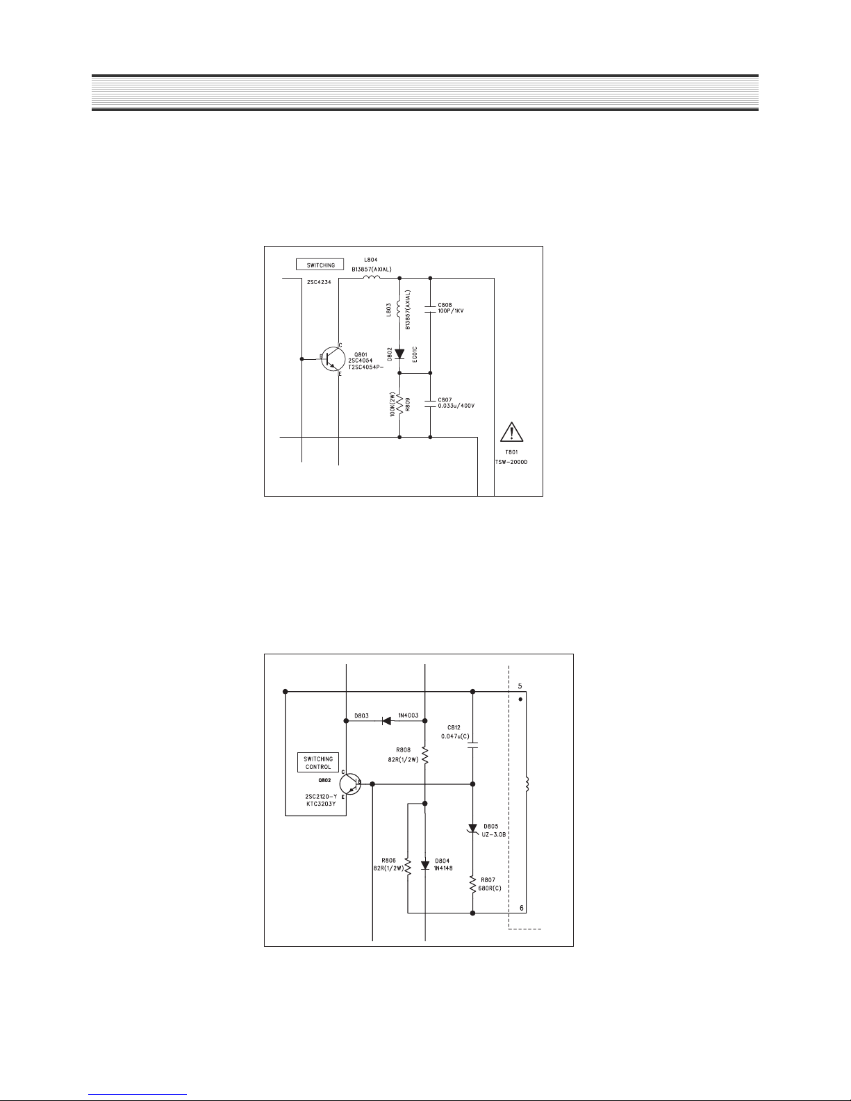
3) Snubber circuit
Snubber circuit protects speedy voltage rising between Collector and Emitter when Main Switching TR is turned off.
So Collector and Emitter voltage enter into safety operation and noise is decreased. When TR is turnd off, because
high reverse voltage is generated between Collector and Emitter, it is rectified to D802, smoothed to C807 and
consumed to R809. C808 is Speed-Up Capacitor.
4) Switching and Control Drive Circuit
When Base of TR is charged through starting part, TR is turned on. So voltage is added to primary winding of
transformer and genertaed at Base Drive. Because this voltage becomes to Positive Feedback voltage, TR is
turned on again and Primary Winding of Trans is charged with electricity .
Picture 4 [Drive Circuit]
18
CIRCUIT OPERATIONAL DESCRIPTION
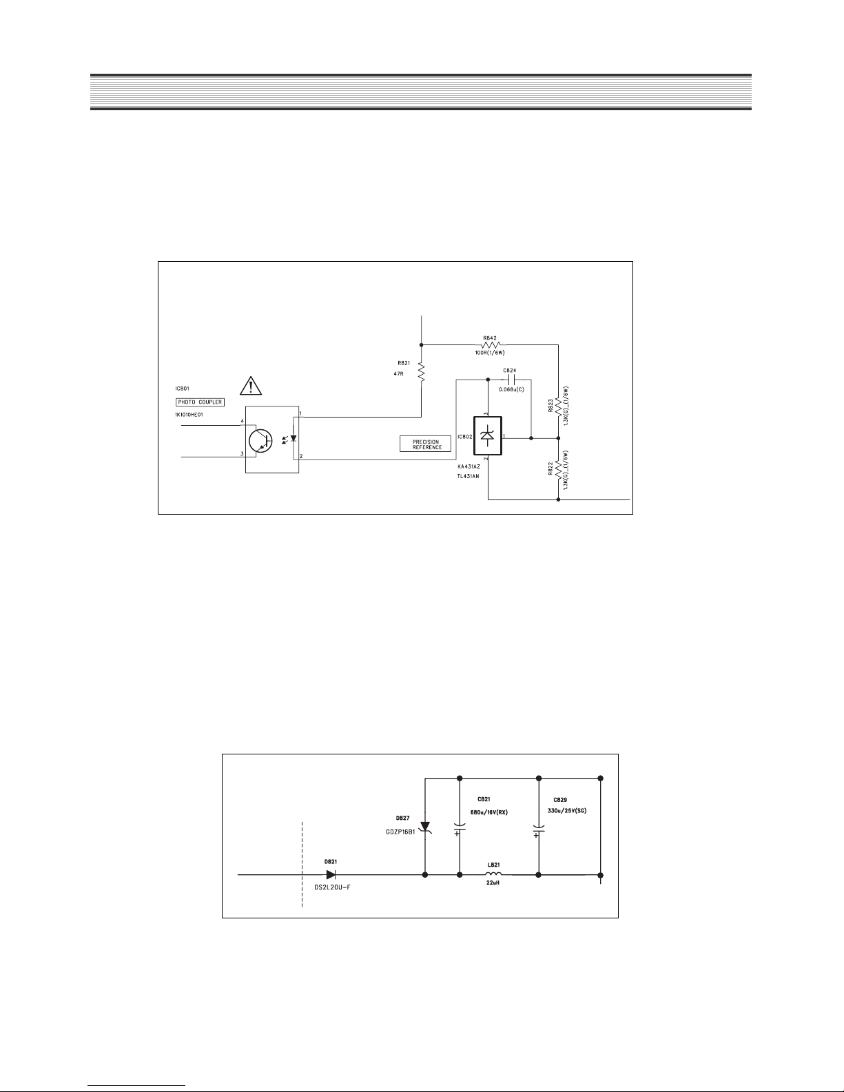
5) Costant-voltage Circuit
This circuit maintains constant voltage. When voltage is lower or higher than reference voltage(2.5V) of IC802 pin1,
this circuit compensates for a loss. Base voltage of Switching TR is controlled and final voltage is regulated by
increasing or decreasing Internal Diode Current of IC801.
Picture
5 [
Costant-voltage Circuit
]
6) Secondary rectification circuit
This circuit generates DC voltage needed to each terminal. It is rectified half-wave by D821, passes through
Electrolytic Condenser C821 and generates the rectified DC voltage. DC voltage passes through L821, C829 of
LC filter and is removed of Ripple and Noise. The other terminal operation is same like this.
Picture
6 [
Secondary rectification circuit
]
19
CIRCUIT OPERATIONAL DESCRIPTION
7) Output terminal
When power is turned off at power applied status, High signal (+3.3V) is applied to Q804 Base terminal and GND
is applied to Q803 Base terminal therefore +5VD is not applied to Q803 emitter terminal and only MVCC(+5V) is
applied to Q803 collector terminal line.
When power is turned on, Low signal(0V) is applied to Q804 Base terminal and Q804 is shorted. At this time,
Q803 Base terminal becomes High status and Q803 is activated. Therefore Q803 outputs +5VD to Emitter
terminal.
2. POWER SUPPLY BLOCK DIAGRAM
Picture
7 [
Output terminal
]
20
CIRCUIT OPERATIONAL DESCRIPTION
FRONT SECTION
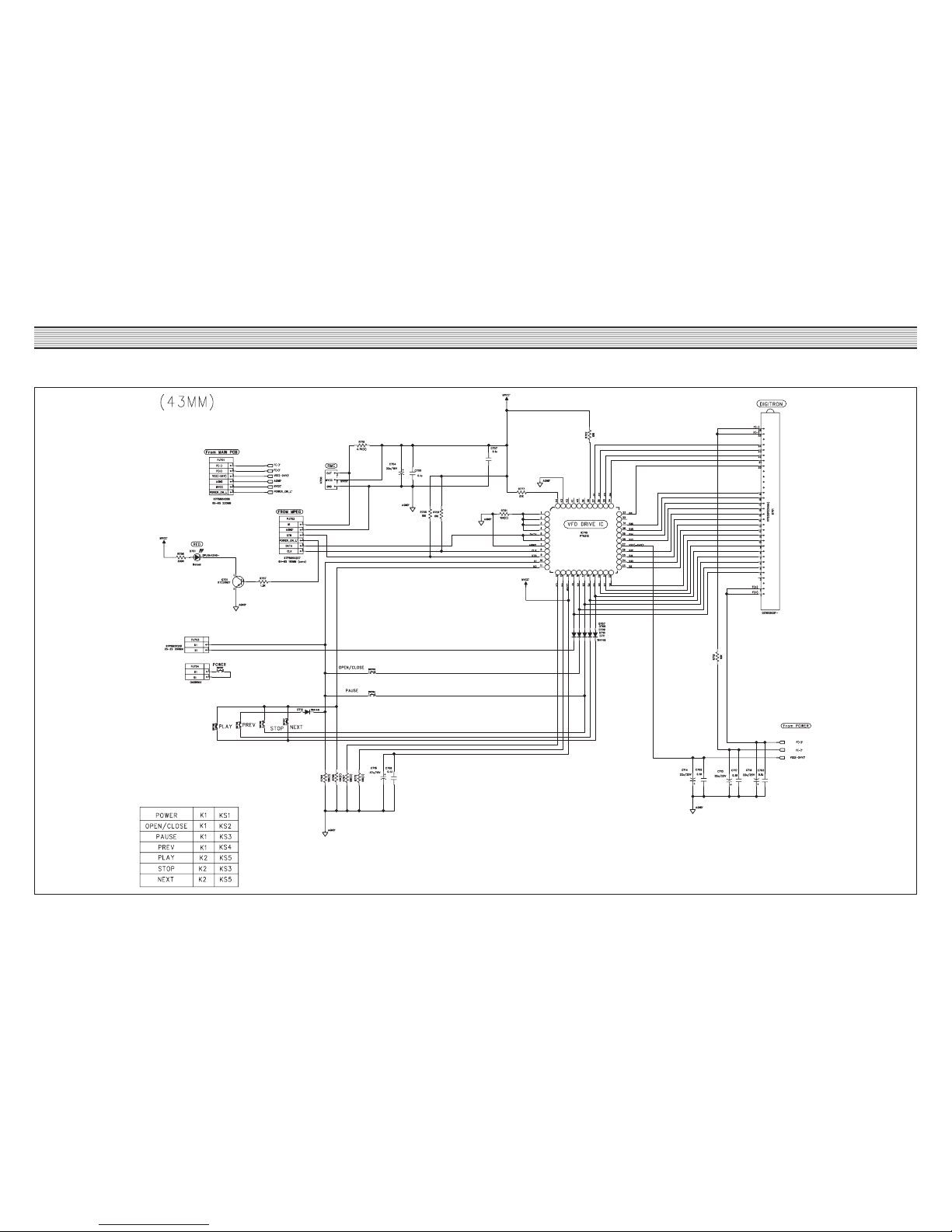
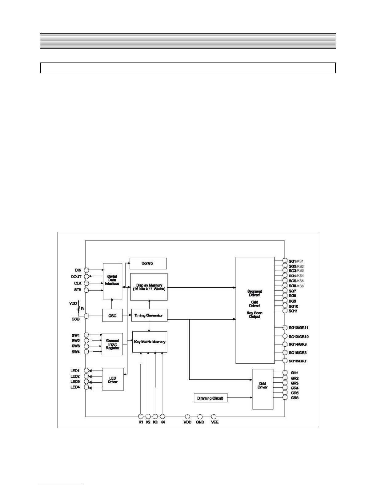
1. VFD DRIVER
1) Overview
IC710 implements following functions by serial communication with MICOM depending on the software.
* CMOS Technology
* Key Scanning(6 x 4 matrix)
* Multiple Display Mode : (11 segments, 11 digits to 16 segments, 6 digits)
* 8-step Dimming circuitry
* LED Ports Provided(4 channels, 20mA max.)
* 4-Bits general Purpose Input Ports Provided
* Serial Interface for Clock, Data Input, Data Output, Stobe Pins
* No External Resistors Needed for Driver Outputs
2) Input/output port description
* Input : Receive the serial data from MICOM when rising edge on Shift clock. And, receive the key of tact switch.
* Output : Output the serial data to MICOM when falling edge on Shift clock. And, display it through digitron with
input data.
3) Internal BLOCK DIAGRAM
21
CIRCUIT OPERATIONAL DESCRIPTION
2. Front Part Operational Description
1) KEY SCAN & VFD Driver(PT6312) Interface
2) Operation Description
* If user presses KEY while IC01(ALI_M3351_2) implements KEY SCAN using VFD DRIVER(PT6312), the
KEY input DATA go to IC01 by SERIAL Communication, then IC01 analyzes and processes the input DATA.
* Implement the operation according to the input command and display the processing status on the VFD
through PT6312.
VFD DISPLAY
VFD DRIVER
(PT6312)
KEY MATRIX
(FRONT TACT SWITECH)
POWER
OPEN/CLOSE
PAUSE/STEP
MICOM INTERFACE
KEY MATRIX
(TACT SWITCH OF 4 DIRECTION)
PLAY
STOP
FFREW
KEY MATRIX
(SHUTTLE RING)
REW FF
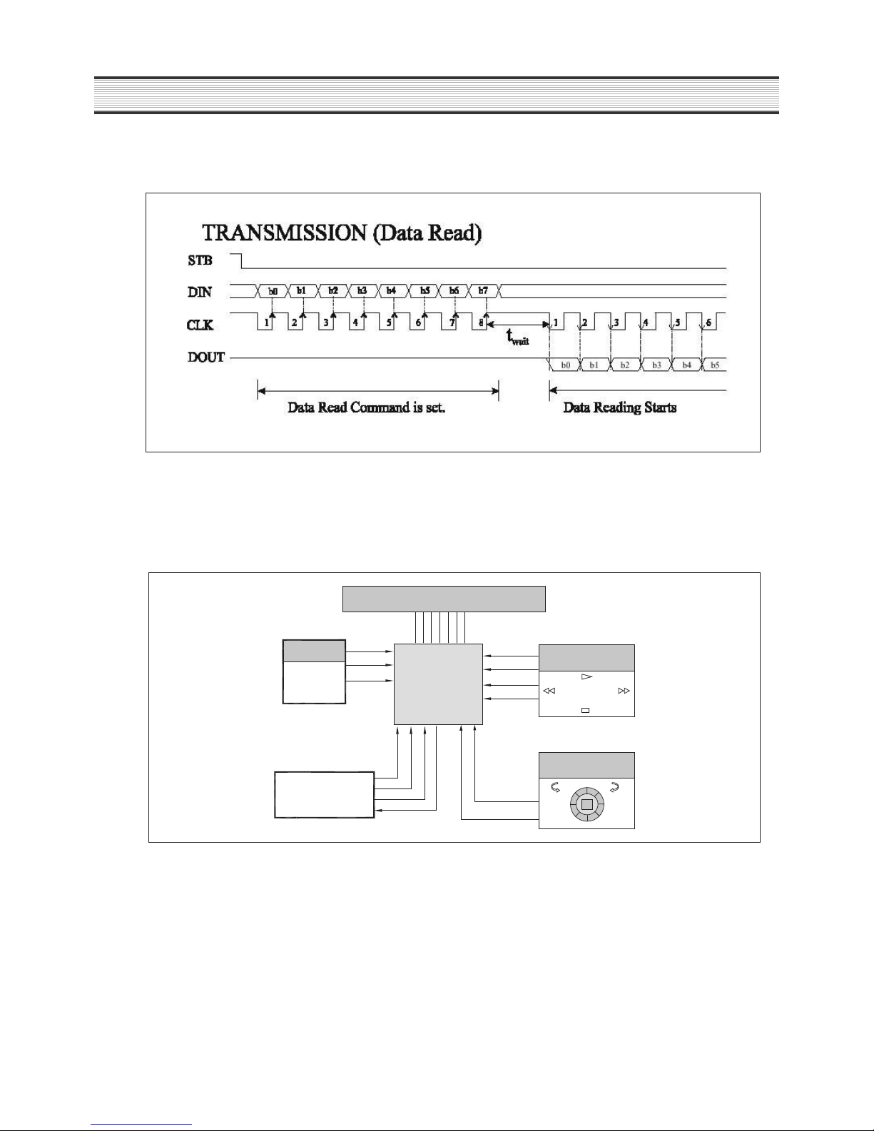
4) Serial Communication Format
22
CIRCUIT OPERATIONAL DESCRIPTION
AUDIO SECTION
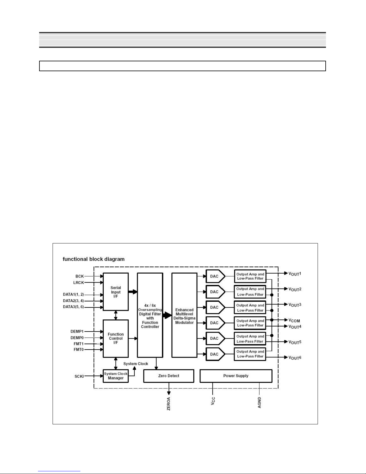
1. 5.1 CH AUDIO DAC IC(IB01) : PCM1606E
1) Overview
24-BIT, 192-kHZ SAMPLING
6-CHANNEL
ENHANCED MULTILEVEL
DELTA-SIGMA DIGITAL-TO-ANALOG CONVERTER
2) Functions
It, as a 5.1CH D/A converter IC, transforms Digital signals to Analog signals by receiving 3 CLOCK (System CLOCK,
Shift CLOCK, Left and Right CLOCK) and 3 DATA from MPEG DECODER.
Each 3 DATA associates to 2 CHANNELS.
->DATA1 : Main L.R CHANNEL
->DATA2 : Surround L.R CHANNEL
->DATA3 : Center, Woofer CHANNEL
During Downmix, it receives only DATA1 from MPEG DECODER.
cf) Downmix : Sound mixing method using 2 CH when the user doesn't have 6 CH amps or speakers but only have 2
CH.
3) Internal Block Diagram
23
CIRCUIT OPERATIONAL DESCRIPTION
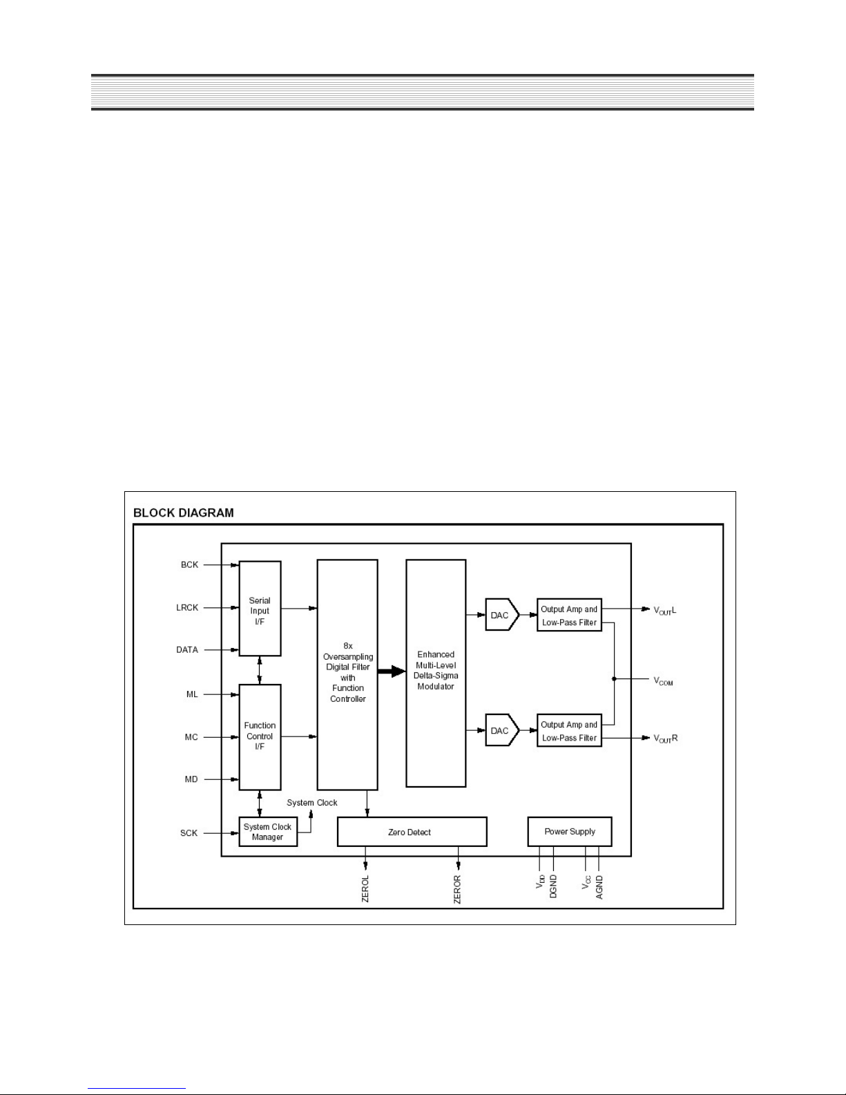
2. 2CH AUDIO DAC IC(IB02) : PCM1748KE
1) Overview
24-BIT, 96-Khz sampling
Enhanced multilevel
Delta-sigma Digital-to-Analog Converter
2) Functions
It, as a 2CH D/A CONVERTER IC, receives 3 CLOCK and 1 DATA from MPEG DECODER and 3 MODE control
signal from MICOM, and then outputs Analog signal of L/R Channel.
* MD : Mode Control Data Input
* MC : Mode Control Clock Input
* ML : Mode Control Latch Input
* BCK : Audio Data Bit Clock Input
* LRCK : L-Channel and R-Channel Audio Data Latch Enable Input
* SCK : System Clock Input
* DATA : Audio Data Digital Input
3) Internal Block Diagram
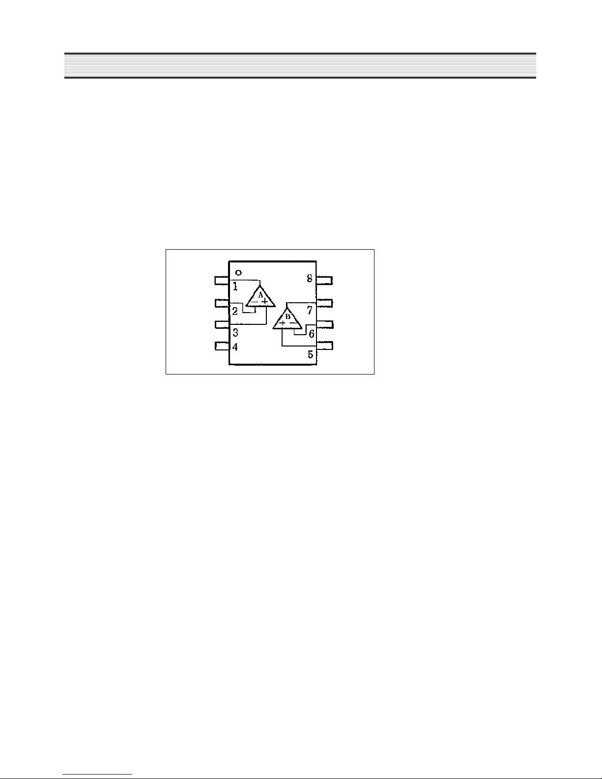
3. OP-AMP IC (IC303, IC304, IC305) : NJM4580M
1) Overview
Dual operational amplifier
2) Functions
It amplifies Analog audio signal from D/A Converter IC.
Each associates to and amplifies 2 channels, and then outputs 5.1 Channel to JK300.
(IC303 : Main L.R, IC304 : Surround L.R, IC305 : Center, subwoofer).
cf) Using 2CH Audio DAC IC (IB02) model outputs 2 Channels to JK101 or JK301 using only OP-AMP IC (IC 303).
3) Internal Block Diagram
24
CIRCUIT OPERATIONAL DESCRIPTION
25
CIRCUIT OPERATIONAL DESCRIPTION
CH
CH
OUTPUT
OUTPUT
JK101 OR JK301
JK101 OR JK301
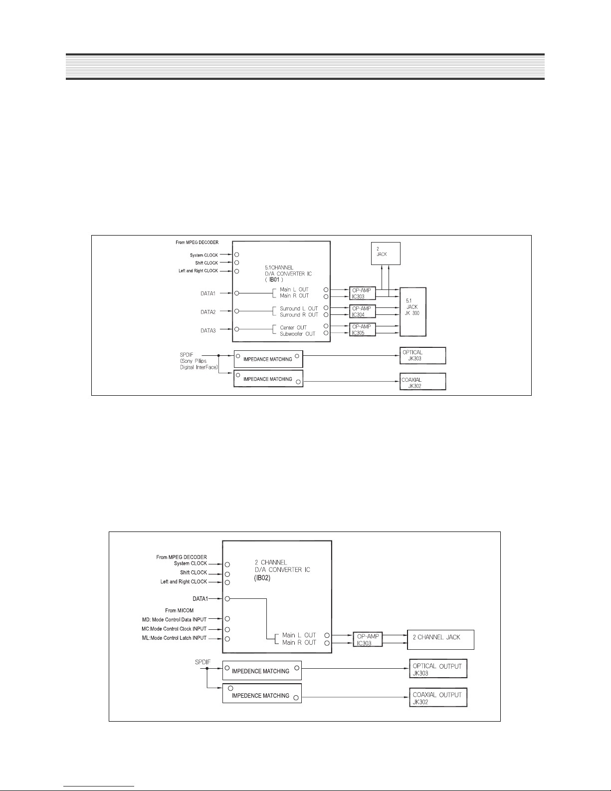
4. General Audio Operation for 5.1CH
1) Overview
It receives CLOCK and DATA from MPEG DECODER(IC01) and transforms Digital signal to Analog signal at AUDIO
D/A CONVERTER(IB01) then, amplifies Analog signal(IC303, IC304, IC305)and outputs to 5.1 CH Jack(JK300) and
2CH Jack(JK101 or JK301).
Receive the digital signal from MPEG DECODER(IC01) and match impedance and then, output the digital signal
through the coaxial jack (JK302) and the optical Jack (JK303).
2) 5.1CH Audio Block Diagram
5. General Audio Operation for 2CH
1) Overview
It receives CLOCK and DATA MODE CONTROL signal from MPEG DECODER(IC 01) and transforms Digital
signal to Analog signal at AUDIO D/A CONVERTER(IB 02) then, amplifies Analog signal(IC303) and outputs to
2CH Jack(JK101 or JK301).
Receive the digital signal from MPEG DECODER(IC01) and match impedance and then, output the digital signal
through the coaxial jack (JK302) and the optical Jack (JK303).
2) 2CH Audio Block Diagram
 Loading...