DAEWOO DP-42GM, DP-42GP, DP-42SM, DP-42SP, DP-42WM Service Manual
...
Service Manual
42" PLASMA PDP MONITOR
CHASSIS : SP-115
S/M No. : DSP115BEF0
Nov. 2002
DAEWOO ELECTRONICS Corp.
http : //svc.dwe .co.kr
Contents
1.Safety Precaution 5
2. Product Specification 6
2-1. SPECIFICATION 6
2-2. Available Input Signal 8
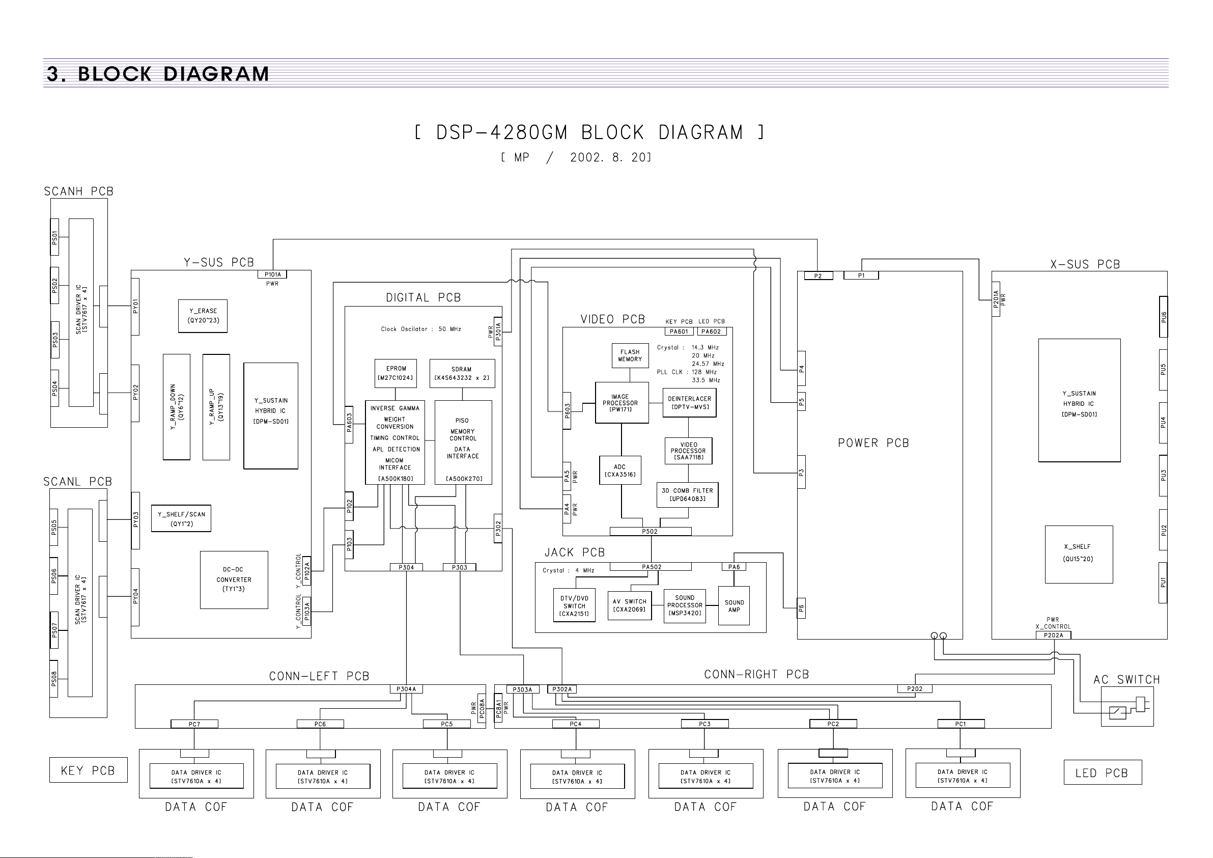
3. BLOCK DIAGRAM 10
4. Description Of Each BLOCK 11
4-1. A/V BLOCK 11
4-1-1. A/V BLOCK DIAGRAM 11
4-1-2. VIDEO PCB 12
4-1-3. JACK PCB 16
4-1-4. KEY PCB 17
4-1-5. LED PCB 17
4-2. DRIVING BLOCK 18
4-2-1. DRIVING BLOCK DIAGRAM 18
4-2-2. DRIVING WAVEFORM 19
4-2-3. DIGITAL PCB 21
4-2-4. X-SUS PCB 25
4-2-5. Y-SUS & SCAN PCB 27
4-2-6. CONNECTION PCB & DATA COF 29
4-3. POWER BLOCK 30
4-3-1. POWER BLOCK DIAGRAM 30
4-3-2. POWER PCB 31
5. SERVICE MODE 33
5-1. Entering SERVICE MODE 33
5-2. Default Values For SERVICE MODE Items 33
5-3. Description Of SERVICE MODE Items 34
6. Adjusting Method 37
6-1. Adjusting WHITE BALANCE 37
6-2. Adjusting DRIVING VOLTAGE And WAVEFORM 38
6-2-1. Adjusting POWER PCB 38
6-2-2. Adjusting X-SUS PCB 39
6-2-3. Adjusting Y-SUS PCB 39
FIG <6-1>. X-SUS PCB Adjusting Points 41
FIG <6-2>. Y-SUS PCB Adjusting Points 42
7. SOFTWARE UPGRADE Method 43
8. SET Disassemble/Assemble Method 46
8-1. Facts You Must Know When Disassembling/Assembling PDP SET 46
8-2. PCB Disassemble/Assemble Method 46
8-3. FRONT MASK Disassemble/Assemble Method 47
8-4. FILTER GLASS Disassemble/Assemble Method 47
-2-
9. Main PCB Trouble Diagnosis 49
9-1. VIDEO & JACK PCB Trouble Diagnosis 49
9-2. DIGITAL PCB Trouble Diagnosis 55
FIG<9-1>. DIGITAL PCB LAYOUT 61
9-3. X-SUS PCB Trouble Diagnosis 62
9-4. Y-SUS & SCAN PCB Trouble Diagnosis 65
9-5. CONNECTION PCB & DATA COF Trouble Diagnosis 71
9-6. POWER PCB Trouble Diagnosis 72
10. TROUBLE SHOOTING 73
10-1. Facts You Must Know When Diagnosing And Repairing 73
10-2. Representative Symptoms When Each PCB Breaks Down 73
10-3. Trouble Diagnosis And Repairing Method For Representative Symptoms 77
FIG<10-1> Trouble Diagnosis Flow when SHUT DOWN occurs 80
FIG<10-2> Trouble Diagnosis Flow when Low Voltage SHUT DOWN occurs 81
FIG<10-3> Trouble Diagnosis Flow when High Voltage SHUT DOWN occurs 82
FIG<10-4> Trouble Diagnosis Flow when Abnormal Discharge occurs 83
11. ASSEMBLY LIST 84
12. EXPLODED VIEW 85
13. FIGURE COLLECTION 86
FIG<1>. TOTAL 86
FIG <2>. Y-SUS & SCAN 87
FIG <3>. X-SUS 88
FIG <4>. VIDEO & JACK 89
FIG <5>. POWER 90
FIG <6>. INLET 91
FIG <7>. LEFT-UP 92
FIG <8>. LEFT-DOWN 93
FIG <9>. RIGHT-UP 94
FIG <10>. RIGHT-DOWN 95
FIG <11>. WITHOUT JACK 96
FIG <12>. DIGITAL 97
FIG <13>. AC SWITCH ASSEMBLY 98
FIG <14>. SCAN ASSEMBLY1 99
FIG <15>. SCAN ASSEMBLY2 100
FIG <16>. X-SUS ASSEMBLY 101
FIG <17>. FRONT MASK ASSEMBLY 102
FIG <18>. FRONT MASK INSIDE 103
FIG <19>. BACK COVER 104
FIG <20>. POWER ADJUSTING POINTS 105
FIG <21>. POWER HIGH VOLTAGE SWITCH 106
FIG <22>. HOW TO ADJUST VOLTAGE 107
-3-
FIG <23>. Y-SUS & SCAN PCB DIODE TEST 108
FIG <24>. SCANH PCB DIODE TEST 109
FIG <25>. SCANL PCB DIODE TEST 110
FIG <26>. 5 STEP GRAY SCALE PATTERN 111
14. Trouble Symptom Picture 112
Trouble Symptom Picture<1>. 112
Trouble Symptom Picture <2>. 113
Trouble Symptom Picture <3>. 114
Trouble Symptom Picture <4>. 115
Trouble Symptom Picture <5>. 116
Trouble Symptom Picture <6>. 117
Trouble Symptom Picture <7>. 118
Trouble Symptom Picture <8>. 119
Trouble Symptom Picture <9>. 120
Trouble Symptom Picture <10>. 121
Trouble Symptom Picture <11>. 122
Trouble Symptom Picture <12>. 123
-4-

1. Safety Precautions
-5-
(1) When moving or laying down a PDP Set, at least two people must be working. Avoid any impact
towards the PDP Set.
(2) Do not leave the broken PDP Set on for a long time. To prevent any further damages, after check the
broken Set
s condition, make sure to turn the power (AC) off.
(3) When opening the BACK COVER, turn off the power (AC) to prevent electric shock. When a PDP is
on, high voltage and high current exist inside the Set.
(4) When loosening screws, check the connecting position and type of the screw. Sort out the screws and
store them separately. Because screws holding PCB are working as electric circuit GROUNDING,
make sure to check if any screw is missing when assembling.
(5) If you open the BACK COVER, you will see a Panel Gas Exhaust Tube (refer to FIG<10>). If this
part is damaged, entire PDP PANEL must be replaced. Therefore, when working, be careful not to
damage this part.
(6) A PDP Set contains different kind of connector cables. When connecting or disconnecting connector
cables, check the direction and position of the cable beforehand.
(7) When disconnecting connectors, unplug the connectors slowly with care. Especially when
connecting/disconnecting FFC (film) cables or FPC cables, do not unplug the connectors too much
instantaneously or strongly, and always handle the cables with care. (Refer to FIG<10>, FIG<11>)
(8) Connectors are designed so that if the number of pins or the direction does not match, connectors will
not fit. When having problem in plugging the connectors, make sure to check their kind, position,
and direction.
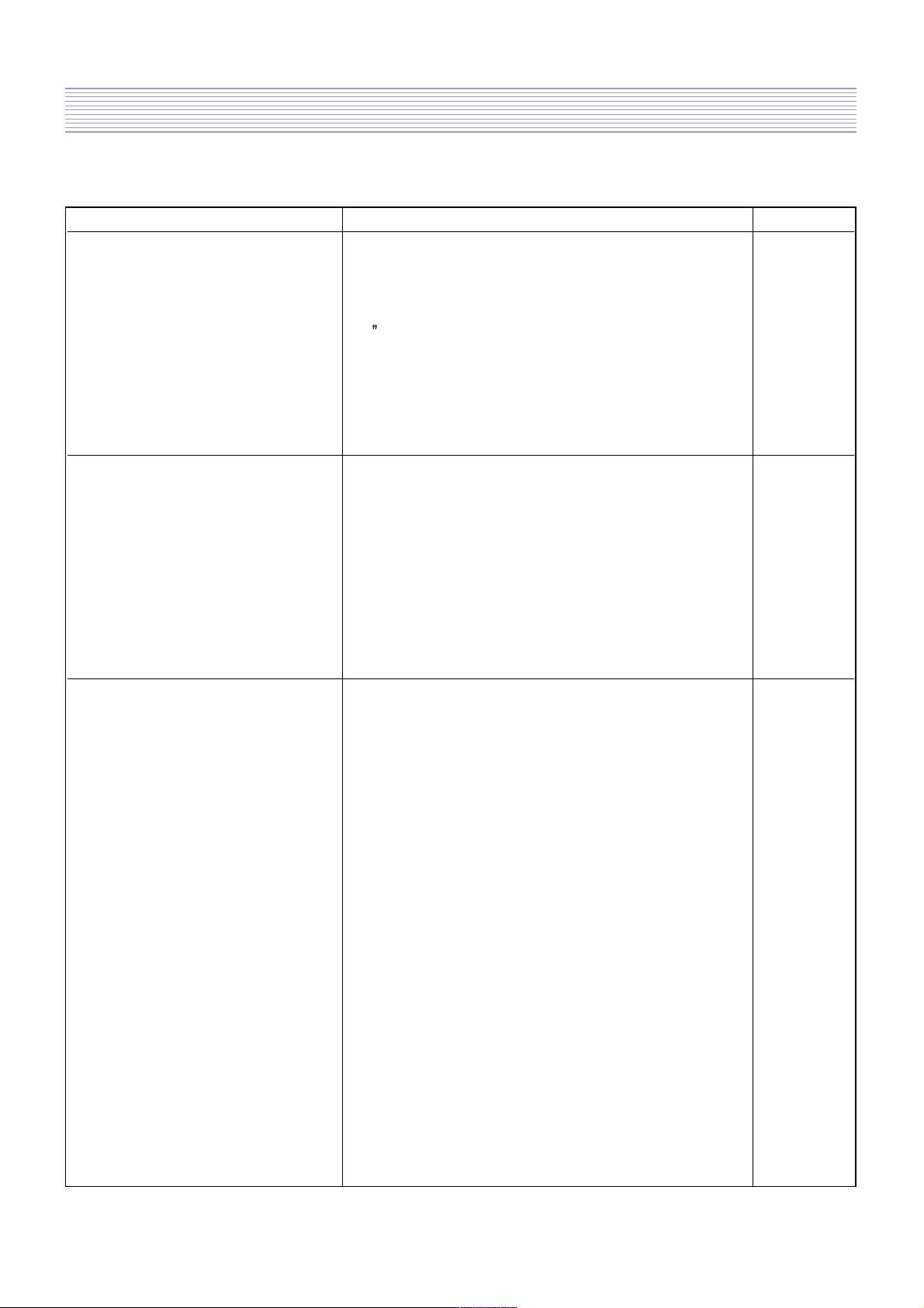
2. Product Specification
-6-
I T E M S P E C I F I C A T I O N REMARK
1. GENERAL
1-1. MODEL NO DSP-4280GM(G, W, S)
1-2. CHASSIS NO SP-115
1-3. SCREEN SIZE 42 (16:9)
1-4. COUNTRY WORLD WIDE
1-5. RESOLUTION 853(H) X 480(V)
1-6. REMOCON TYPE R-V28A (E)
1-7. SAFETY STANDARD UL, C-UL, CE, CB, FCC(CLASS B), CE(CLASS B), K-mark
2. MECHANICAL
2-1. APPEARANCE
1) WITHOUT STAND WxHxD=1,039 x 628 x 80 mm
2) WITH STAND WxHxD=1,039 x 725 x 320 mm
3) CARTON BOX WxHxD=1,256 x 800 x 327 mm
2-2. WEIGHT
1) WITHOUT STAND 29.9 Kg
2) WITH STAND 36.8 Kg
3. ELECTRICAL
3-1. VIDEO INPUT COMPOSITE(NTSC, PAL, SECAM, PAL-M/N, NTSC4.43)
& S-VHS(50/60Hz Y/C) 2 sets
3-2. DTV/DVD INPUT 1080 i, 720P, 480P , 480i
(Y, Pb/Cb, Pr/Cr COMPONENT SIGNAL) 2 sets
3-3. PC INPUT VGA ~ UXGA (15 PIN D-SUB) 1 sets
3-4. SOUND INPUT 2 sets for VIDEO, 2 sets for DTV/DVD, 1 set for PC
3-4. SPEAKER OUTPUT 8W(R) + 8W(L)
3-5. POWER REQUIREMENT AC 100V~240V, 50/60Hz
3-6. POWER CONSUMPTION 320W
3-8. RS-232 CONTROL RS-232 Communication (for SOFTWARE UPGRADE)
3-9. FUNCTION
1) SCALING PC: H/V SIZE and POSITION Adjusting
VIDEO/DTV/DVD : NOMAL, 16:9, PANORAMA, ENLARGE
LB, ENLARGE LBS
2) ZOOM 20 Scale ZOOMING & PANING
3) OSD Support 11 Languages
4) OTHERS STILL, SLEEP MODE, SOUND MODE
2-1. PRODUCT SPECIFICATION
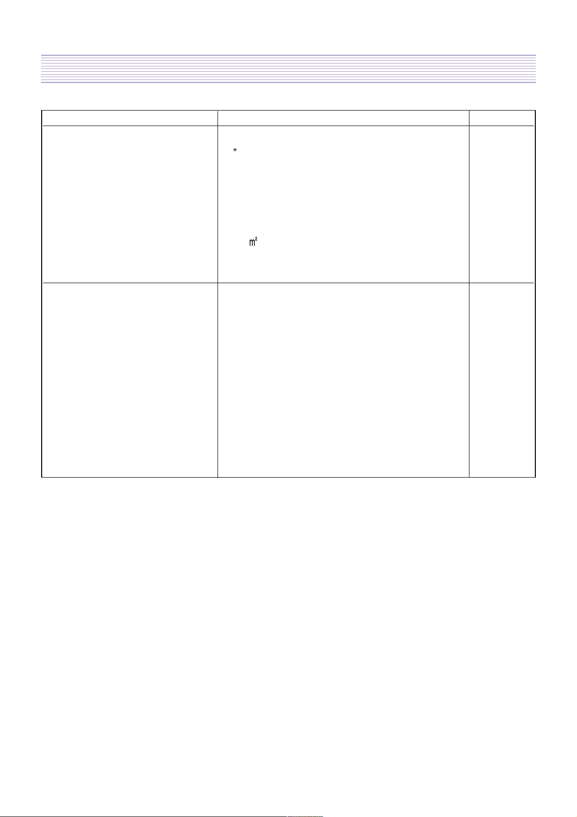
Product Specification
-7-
I T E M S P E C I F I C A T I O N REMARK
4. OPTICAL
4-1. SCREEN SIZE 42 (106Cm) DIAGONAL
4-2. ASPECT RATIO 16:9
4-3. NUMBER OF PIXELS 853(H)X480(V)
4-4. DISPLAY COLOR 16.77 Million Colors ( 8BIT per each R,G,B)
4-5. PIXEL PITCH 1.08(H)X1.08(V)
4-6. PEAK LUMINANCE 300cd/ (WITH FILTER GLASS)
4-7. CONTRAST RATIO 3000:1
4-8. VIEWING ANGLE Over 160 degree ( VERTICAL / HORIZONTAL)
5. USERCONTROL & ACCESSORIES
5-1 CONTROL BUTTON(SET) AC POWER BUTTON(PUSH-PULL S/W)
MENU, SELECT, UP, DOWN, LEFT, RIGHT(SOFT S/W)
5-2. REMOTE CONTROL(R-V28) POWER, INPUT SELECT, DISPLAY, ZOOM-,ZOOM+,
MENU, UP, DOWN, VOLUME, FREEZE, SCREEN MODE,
SOUND MODE, SLEEP
5-3. ACCESSORIES REMOCON CONTROLLER, BATTERY,
INSTRUCTION MANUAL, A/V CABLE,
STAND, WALL HANGER, SPEAKER R/L
Product Specification
-8-
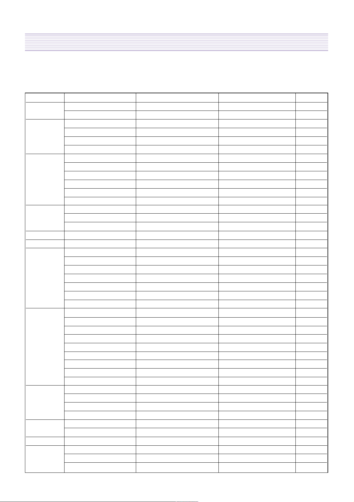
Resolution H Freq. (KHz) V Freq. (Hz) Remark Patt No.
640x350 31.469 70.1 IBM 203
37.861 85.1 VESA 11
640x400 24.823 56.4 NEC 15
30.48 60.0 PGA 871
31.469 70.1 IBM (DOS) 204
37.861 85.1 VESA 16
640x480 31.469 59.9 DOS 17
35 66.7 Macintosh 18
37.861 72.8 VESA 19
37.5 75.0 VESA 20
39.375 75.0 IBM 21
43.269 85.0 VESA 22
720x400 31.47 60.0 VGA 876
31.469 70.1 IBM 13
37.927 85.1 VESA 14
720X480 31.54 60.0 480P 953
720X576 15.63 25.0 PAL 950
800x600 35.156 56.3 VESA 23
35.16 57.2 VESA 24
37.879 60.3 VESA 24
48.077 72.2 VESA 25
46.875 75.0 VESA 26
53.674 85.1 VESA 27
832x624 49.726 74.0 Macintosh 28
1024x768 48.193(48.077) 59.3(59.8) Macintosh(OAK) 29
48.363 60.0 VESA 30
53.95 66.1 XGA 890
56.476 70.1 HP&VESA 31
60.241 74.9(74.6) Macintosh 32
60.023 75.0 VESA 33
68.677 85.0 VESA 34
80.66 100.0 Fujitsu 939
70.84 84.0 SUN 926
1152X864 54 60.0 VAX 936
63.851 70.0 VESA 35
67.5 75.0 VESA 36
77.094 85.0 VESA 37
1152x900 61.796 66.0 SUN 38
71.713 76.0 SUN 39
1280X720 45 60.0 720P 954
1280X960 60 60.0 VESA 40
75 75.0 VESA 41
85.938 85.0 VESA 42
2-2. Available Input Signal
(1) PC
-9-
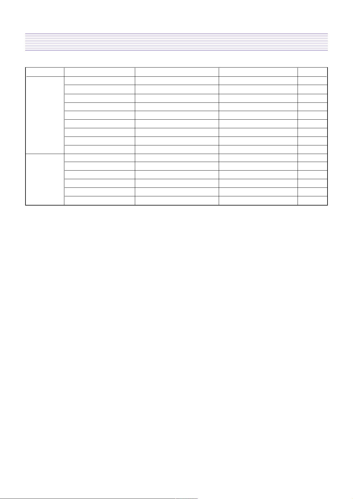
Product Specification
Resolution H Freq. (KHz) V Freq. (Hz) Remark Patt No.
1280X1024 46.433 43.4 VESA 205
63.981 60.0 VESA 44
70.66 66.5 VAX 937
74.88 70.0 NEC 921
78.125 72.0 HP & HITA 206
78.855 74.1 Sony & NEC 46
79.976 75.0 VESA 47
81.13 76.1 SUN 927
91.146 85.0 VESA 48
1600X1200 62.5 48.0 VESA
75 60.0 VESA 50
81.25 65.0 VESA 862
87.5 70.0 VESA 863
93.75 75.0 VESA 864
100 80.0 VESA 865
(2) DTV
-1080i/ 60 Hz
-720P / 60 Hz
-480P / 60 Hz
(3) VIDEO
-PAL, PAL-M, PAL-N
-NTSC , NTSC4.43
- SECAM
-10-
-11-
4. Description Of Each BLOCK
4-1. A/V BLOCK
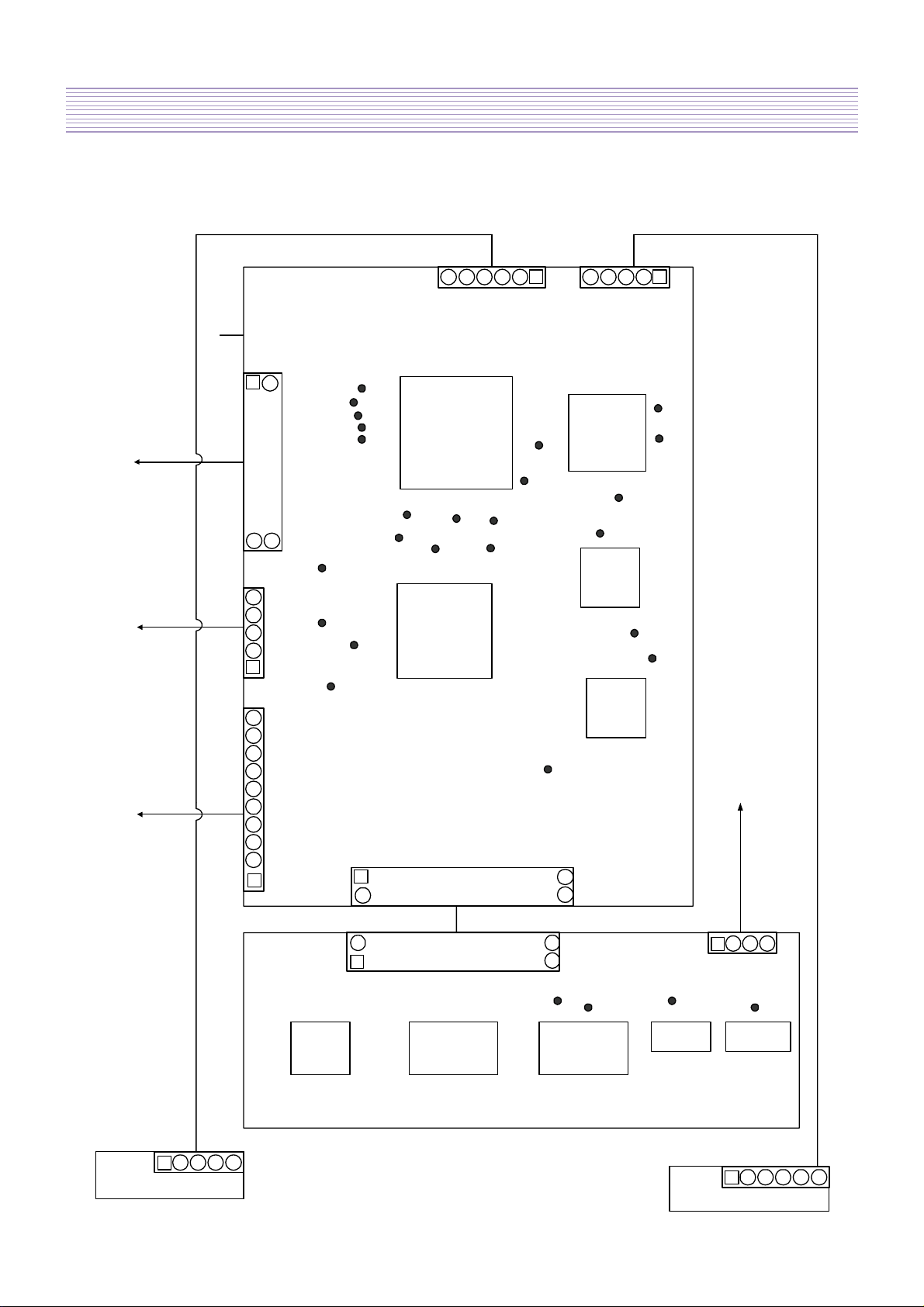
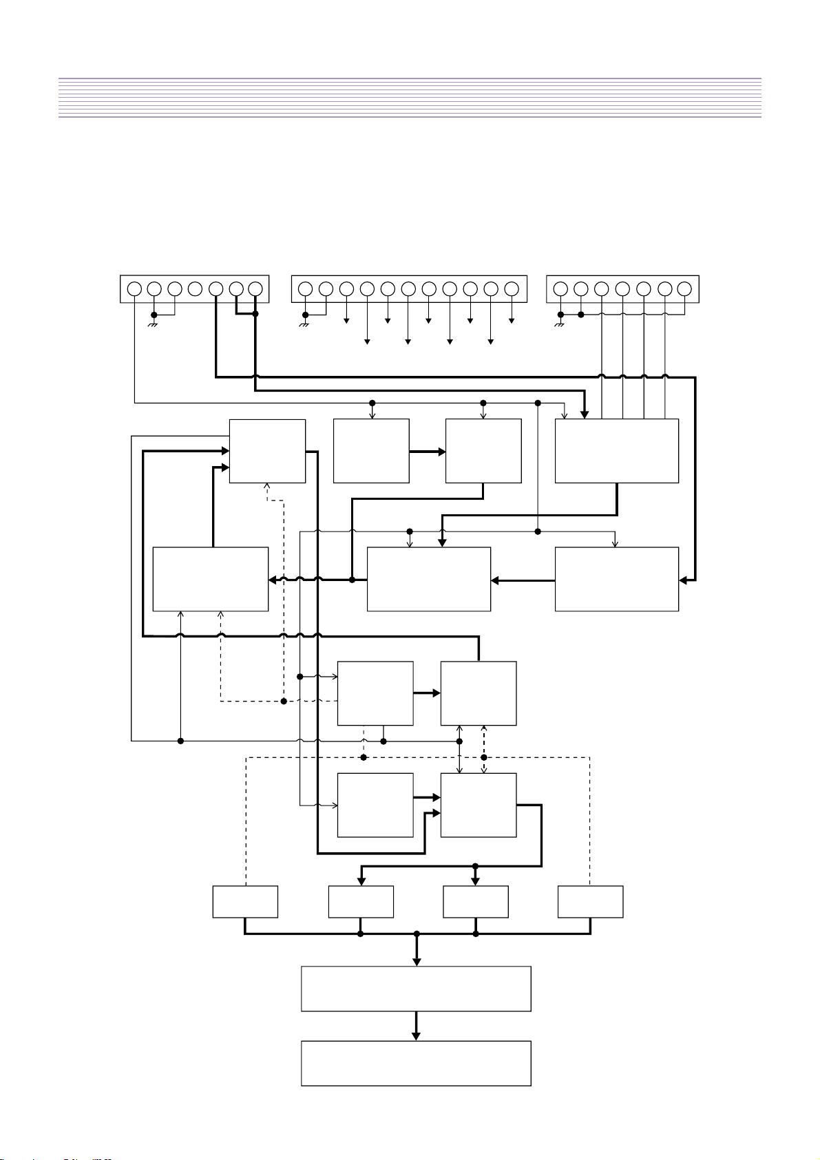
4-1-1. A/V BLOCK DIAGRAM
to PWR
to
DIGITAL
to PWR
P602P601
P12V
P12V
GND
GND
SEL1
SEL3
GND
SCL
SDA
DSDA
S_MUTE
GND
GND
TXD1
RXD1
GND
DSCL
GND
NC
SEL2
NC
ID_JACK
GND
MSP_RST
GND
P502
1
50
26
25
1
5026
25
PA6
1
432
PA502
JACK
PCB
GND
IR
P_LED
GND
S5V
1
5
4
3
2
COLUM1
COLUM2
COLUM3
DATA1
DATA2
GND
1
5
432
6
P603
2
GND
G0
G1
G2
G3
G4
G5
G6
G7
GND
B0
B1
B2
B3
B4
B5
B6
B7
GND
DCLK
STB5V
NC
NC
NC
DVS
DHS
V_MUTE
S_RESET
NC
DEN
GND
R0
R1
R2
R3
R4
R5
R6
R7
GND
39
1
40
PA4
1
6
7
8
9
5
3
4
2
STB5V
LED_P
GND
GND
P5V
GND
GND
P12V
NUL
P12V
1
5
2
3
4
PA5
STB5V
GND
PWR_CLT
LED_P
to PWR
VPC
HPC
GND
BPC
GND
GPC
GND
GND
RPC
GND
G/Y_DTV
GND
B/PB
GND
R/PR
GND
Y_DVD
GND
CB
GND
GND
CO
YO
GND
CR
IC600
PW171
IC406
DPTV-MVS
IC401
SAA7118
IC400
u64083
IC500
CXA3516
DEN
S_RESET
V_MUTE
DVS
DHS
GBLKSLP GPEN
GSOG
GHSFOUT
GCOAST
GREF
GCLK
GHS
GVS
YCOMB
CCOMB
DECOE
VPEN
VHS
VVS
VCLK
VPEN1
PA602
1
5432 6
LED
1
5432
PA601
KEY
PCB
IC706
CXA2151
IC704
CXA2069
IC700
MSP3420
IC702
TDA7480
IC701
TDA7480
R_OUT
L_OUT
RIGHT
LEFT
10
VIN
DCLKB
-12-
Description Of Each BLOCK
4-1-2.VIDEO PCB
- PROCESS Various Signal (PC, COMPONENT, COMPOSITE ) to produce 24BIT DIGITAL
output
1) IC and TP
(1) IC400(UPD64083)
-Using 3D COMBFILTER to separate COMPOSITE signal to Brightness
Signal(Y) and Color Signal(C)
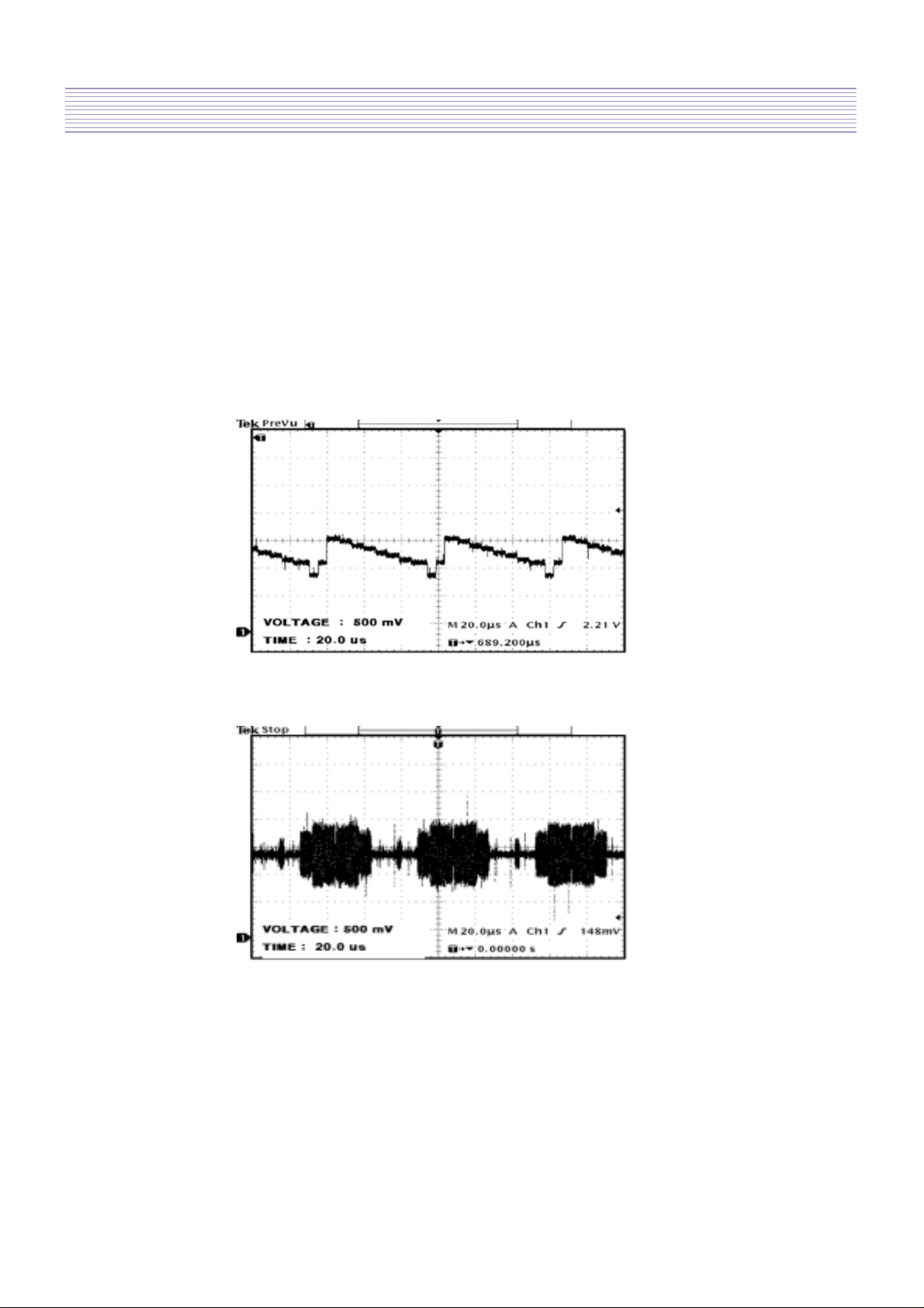
*TP ( Input : COLOR BAR PATTERN )
A. YCOMP : Brightness Signal(Y)
B. CCOMP : Color Signal (C)
(2) IC401 (SAA7118E)
-Receive NTSC, SECAM, PAL VIDEO by COMPOSITE(V) , S-VHS(Y.C)
COMPONENT (Y Cb Cr) and process signal
*TP
A. DECOE : CHIP ENABLE part. When signal process is done by IC401,
output 3.3V DC LEVEL
-13-
Description Of Each BLOCK
(3) IC406(DPTV-MVS)
-A Scan Rate Converter which converts Interlace signal into Progressive signal
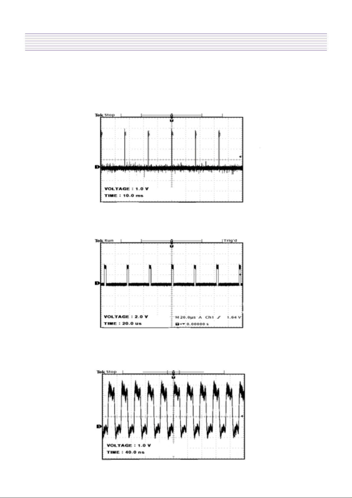
*TP
A. VVS : VERTICAL SYNC (output by DPTV-MVS)
B. VHS : HORIZONTAL SYNC (output by DPTV-MVS)
C. VCLK : CLOCK (output by DPTV-MVS)

-14-
Description Of Each BLOCK
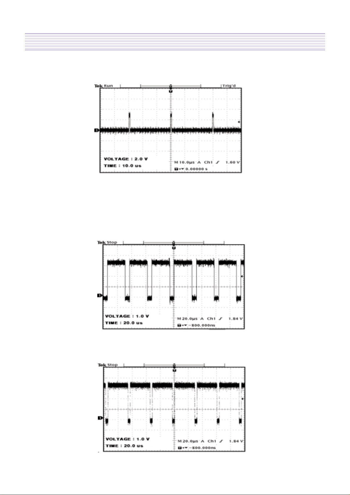
(4) IC500(CXA3516R)
-3-channel 8-bit 165MSPS A/D converter which process PC , DTV signal
* TP
A. GCOAST : COAST CONTOL Signal for PLL (input by CXA3516)
B .GHS : HORIZONTAL SYNC for GRAPHIC (output by CXA3516)
C. GCLK : CLOCK for GRAPHIC (output by CXA3516)
-15-
Description Of Each BLOCK
D. GFBK : SYNC for PLL
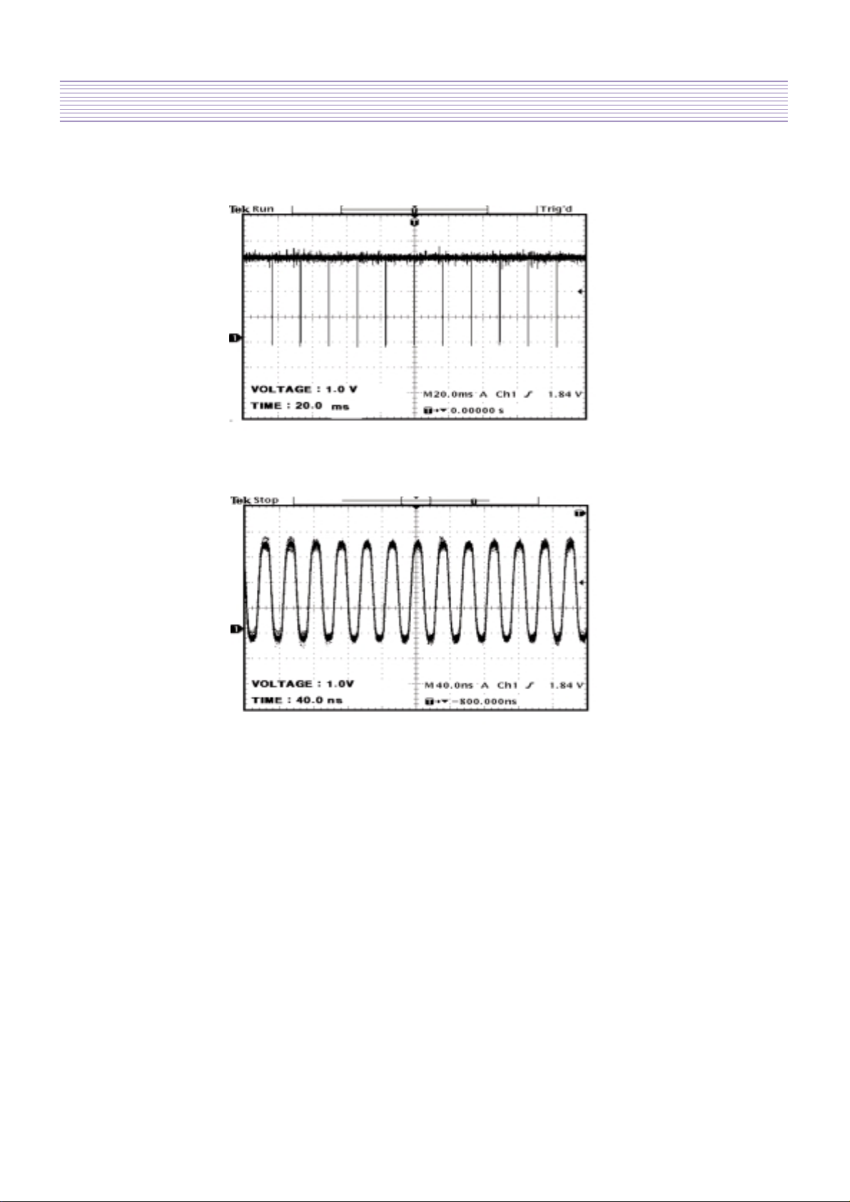
(5) IC600(PW171)
- Image processor IC
*TP
A. DEN : DATA ENABLE (output by PW171)
B. DHS : HORIZONTAL SYNC (output by PW171)
-16-
Description Of Each BLOCK
C.DVS : VERTICAL SYNC for DISPLAY (output by PW171)
D. DCLKB : CLOCK for DISPLAY (output by PW171)
4-1-3. JACK PCB
- Separate and process various VIDEO and AUDIO signal
(1) IC706(VIDEO /SYNC SELECTOR)
- This chooses Y Cb/Pb Cr/Pr or RGB signal to output Y Cb/Pb Cr/Pr, to separate SYNC, and to
perform SYNC COUNTER.
(2) IC704(7_INPUT 3_OUTPUT AUDIO/VIDEO SWITCH)
- The IC perform AUDIO or VIDEO SWITCHING
(3) IC700(MULTI STANDARD SOUND PROCDSSOR)
-AUDIO SINGNAL VOLUME control, EQUALIZER control
-17-
Description Of Each BLOCK
*TP
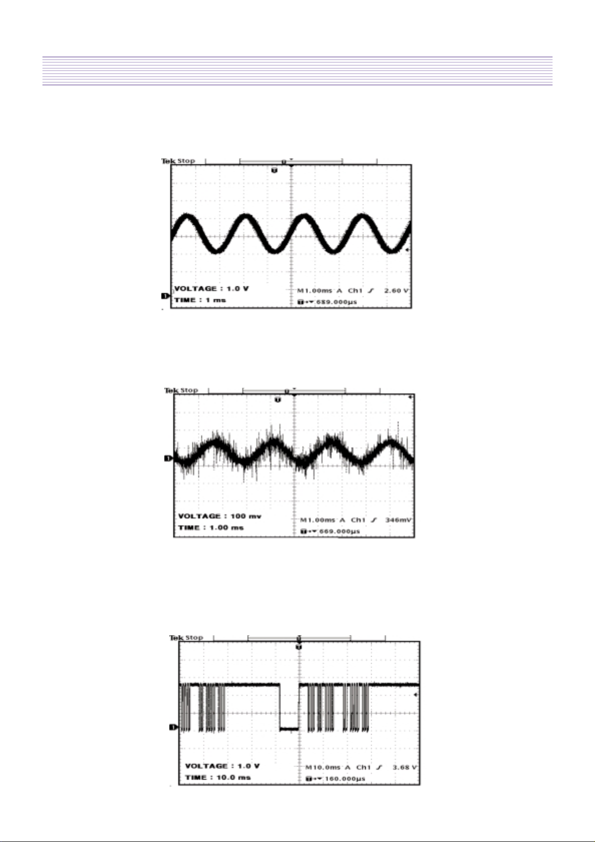
R_OUT(L_OUT) : AUDIO SIGNAL that goes into MSP3420 before AUDIO PROCESSING
(4) IC701 .IC700 (TDA 7480)
*TP
A. RIGHT(LEFT) :AMP input signal before 30dB amplification
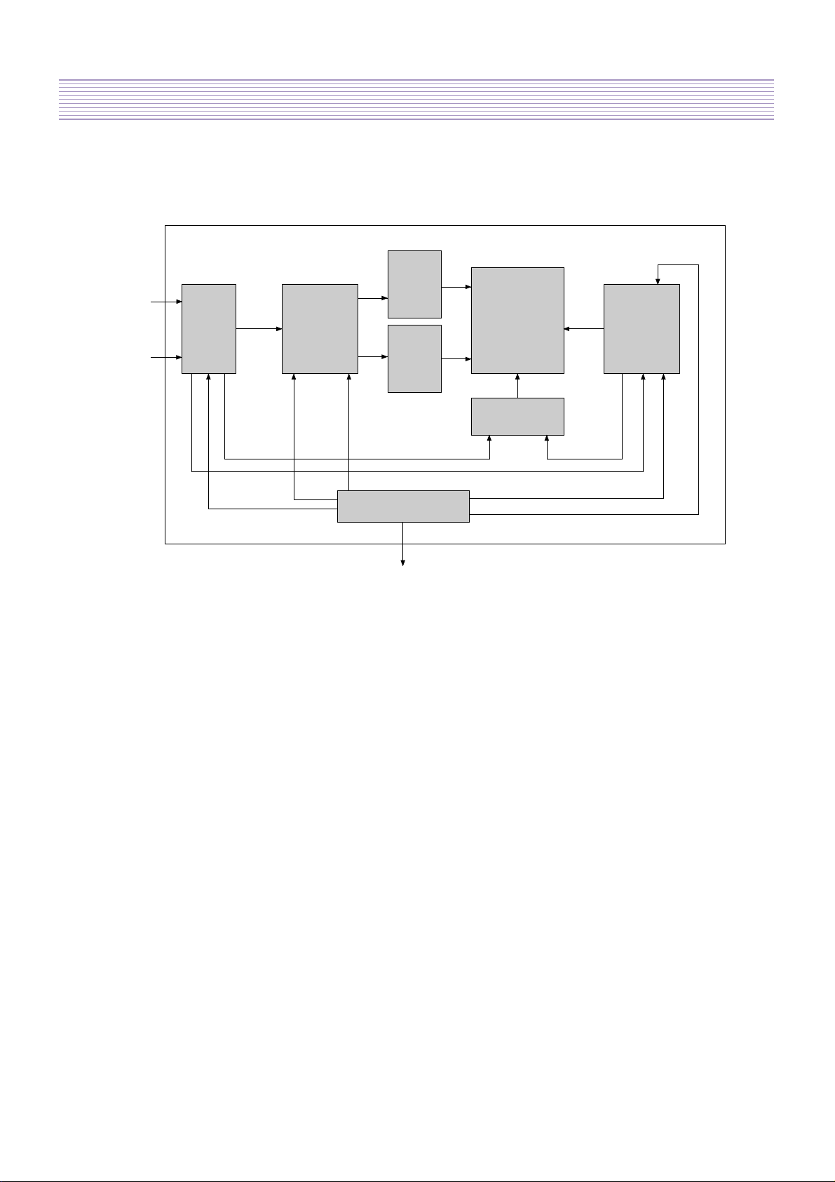
4-1-4.KEY PCB
- Input PCB using KEY
4-1-5.LED PCB
- PCB for REMOCON CONTROL
-18-
Description Of Each BLOCK
4-2 DRIVING BLOCK
4-2-1. Driving BLOCK DIAGRAM
TIMING
CNOTROL
&
DATA
INTERFACE
Y-SUSTAIN
ENERGY
RECOVERY
SCAN
ERASE
WRITING
SCAN
TOP
SCAN
BOTTOM
PANEL
X-SUSTAIN
ENERGY
RECOVERY
SHELF
DATA
DRIVER
DATA
INPUT
CONTROL
SIGNAL
POWER
Verase Vsus
Vsus
Vadd
Vadd
Vdr
Vstb/Video/etc.
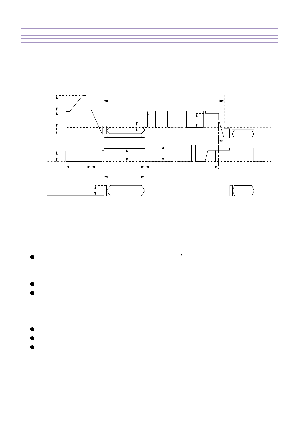
Driving circuit block looks like above diagram. First, within the Digital-board, timing control / data
interface signals input to Y / X / DATA-board. Also, low voltage and high voltage powers such as
15V / 5V / Vsus / Yer / Vadd are supplied. SCAN is divided into two PCB(upper and lower) and
DATA driver can drive 7 COF module. Also Connection-board which is located at the lower part of
the panel, is divided into two PCB. It transfer 5V / Vadd power supply as well as various Y / X /
DATA-board. Vadd power supply is transferred from Power module to X-board through Connectionboard to Data driver.
-19-
Description Of Each BLOCK
4-2-2. Driving Waveform
1 SUB-FIELD
173V
166V
230V
173V
GND
-62V
158V
GND
GND
68V
L
H
X-SHELF
ADDRESSING
FULL WRITING
SUSTAINING
ERASING
173V
155V
Zn
Z-DRIVING
X-DRIVING
Y-DRIVING
BV
Yn
SCAN
163
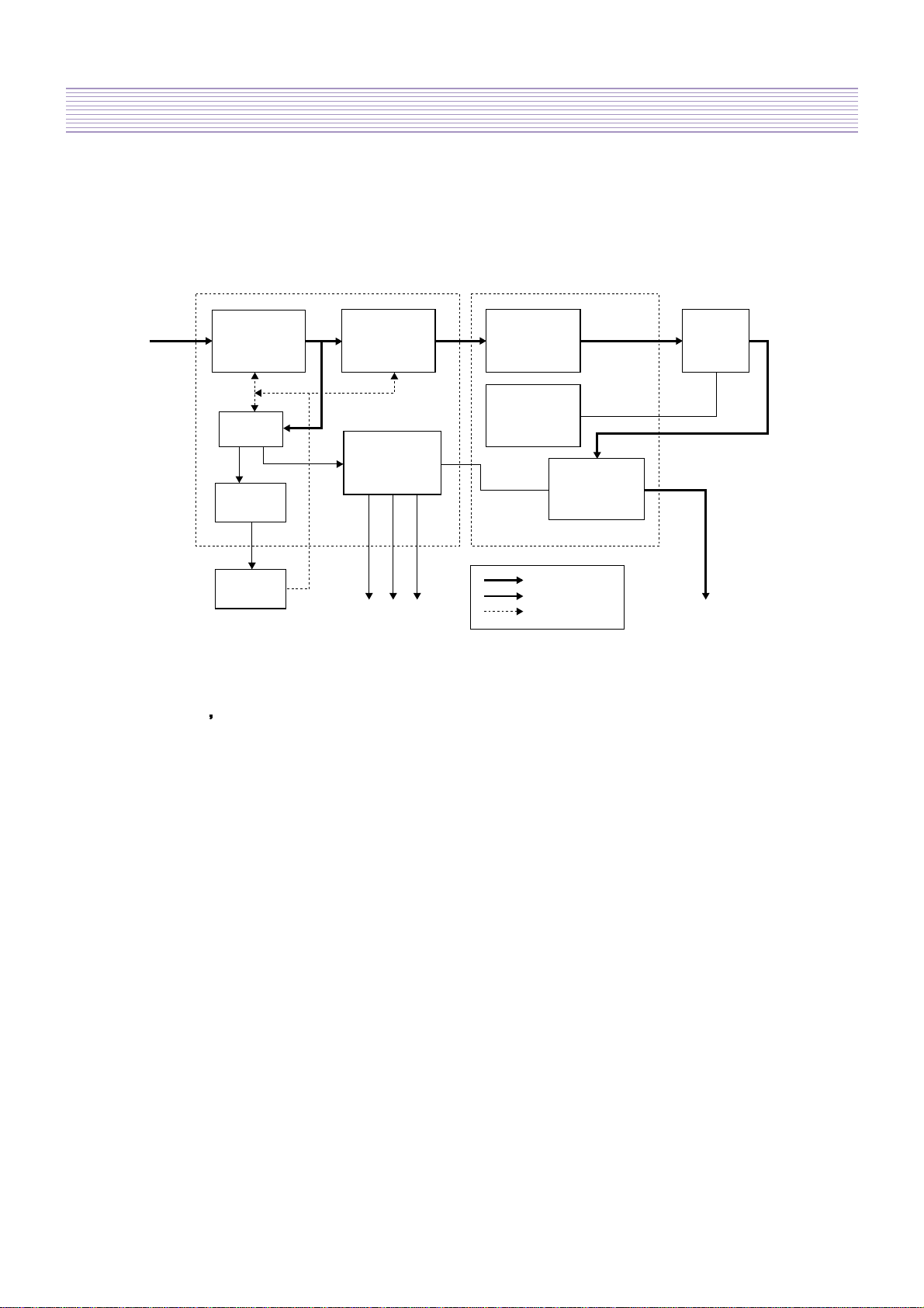
PDP Driving signal is largely divided into three(Y, X, Z) as shown above. They are outputs of Yboard, X-board, DATA-board (COF) respectively. Each Sub-field is divided into ADDRESSING,
SUSTAINING, ERASING parts. FULL WRITE pulse from Y-board adds once per frame(
=
~
16ms).
1) FULL WRITING
It is a process that in order to display new image, every cell s condition must be uniformed to erase
wall charge made by previous discharge and make new wall charge for next address discharge.
Ramp shape signal is added to supply every cell uniform wall charge.
To decrease Background luminescence and improve contrast, it is applied once per frame.
Full Writing signal output by Y-board is Vsus electric potential supplied by power module plus
ramp-shape output signal made by DC-DC Converter(TY1).
2) ADDRESSING
Previous to SUSTAINING, it is procedure to select charging cell for image display.
In other words, it is the stage to make wanted cell to form wall charge.
During this stage, SCAN block operate in Y-board and SHELF block (X_HIGH) in X-board.

-20-
Description Of Each BLOCK
3) SUSTAINING
After the Addressing period, this stage is to add Sustaining pulse to selected cell to make the
SUSTAINING discharge continue.
For each X, Y-board sustain block, opposite-polarity rectangular pulse which have ER_H SUS_H
ER_L SUS_L order, is distributed to Panel s X,Y electrode at a constant frequency.
4) ERASING
Removing operation for Electrical discharge inside each cell to address new data in next Sub-field.
It is a Ramp output signal similar to Full Writing signal.
Ramp-down block operates in Y-board and Shelf block (X_N_SHELF) operates in X-board.
-21-
Description Of Each BLOCK
4-2-3. DIGITAL PCB
ID1
1st_chip(A500K180)
ID2
2nd_chip(A500K270)
ID3 & ID4
RGB DATA [0:3]
Inverse Gamma
&
Dithering
APL
Detection
ROM
(M27C1024)
ROM
Controller
ID33
PISO
PDP Driving
Timing Controller
SDRAM
Controller
SDRAM
(64M x 2)
Data Interface
Weight
Conversion
X Driver Control Signal
Y Driver Control Signal
Z Driver Control Signal
Z Driver Data Signal
: Data Flow
: Control Address Flow
: ROM Data Flow
<DSP-4280GM Digital B/D Block Diagram>
1. Digital PCB s Main Part
(1)Actel FPGA A500K180-PQ208 : 1 EA
- Location No. : ID1
- Power : Internal 2.5V, I/O 3.3V
- Package : PQFP 208
- Typical Gates : 150,000
- User I/O : 164
(2)Actel FPGA A500K270-BG456 : 1 EA
- Location No. : ID2
- Power : Internal 2.5V, I/O 3.3V
- Package : BGA 456
- Typical Gates : 215,000
- User I/O : 362
(3)SDRAM( K4S643232E-TC70 86pin TSOP ) : 2 EA
- Location No. : ID3~4
- Power : 3.3V
- Size : 64 M ( 512K * 32 bit * 4 Banks )

-22-
Description Of Each BLOCK
(4)50MHz Clock Oscillator : 1 EA
- Location No. : XD1
- Power : 3.3V
(5)Buffer IC( 74LCX541 ) : 17 EA
- Location No. : ID9~25
- Power : 5V
- Input Voltage : 3.3V
- Output Voltage : 5V
(6)Buffer IC( 74LCX541 ) : 4 EA
- Location No. : ID5~8
- Power : 3.3V
- Input/Output Voltage : 3.3V
(7)EPROM( M27C1024-PLCC44 ) : 1 EA
- Location No. : ID33
- Power : 5V
- Input Voltage : 3.3V
- Output Voltage : 5V
(8)2.5V Regulator( LP3964EMP-2.5 )
- Location No. : ID32
- Input Voltage : 5V
- Output Voltage : 2.5V
(9)EMI Reduction IC ( P2040 )
- Location No. : ID34
- Power : 3.3V
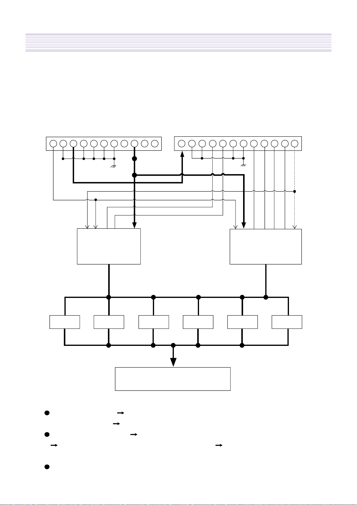
2. Data Flow
(1)Input from Video PCB
- 8bit Data per each R,G,B ( synchronized by DCLK)
- DVS, DHS, DEN, S_RESET, V_MUTE, DCLK(33.5 MHz)
(2)Inverse Gamma & Dithering Block
- After mapping input data according to Reverse Gamma Correction Table , execute
Dithering Process .
(3)Weight Conversion Block
- Map input data according to Weight Conversion Table , which is based on optimum PDP
Driving Weight Pattern.

-23-
Description Of Each BLOCK
(4)ROM & ROM Controller Block
- ROM contains Reverse Gamma Correction Table , Weight Conversion Table , APL
Table and so on. Rom Controller Block generate Address & Control signal for receiving
these data from ROM
(5)PISO(Parallel Input Serial Output) Block
- Load 10 pixels per each R,G,B data with parallel type and shift them with serial type in order
of Weight ( LSB first ). These shifted data is stored in Internal Memory of A500K270(ID2)
with based on DCLK(33.5MHz). After that, those data go into External Frame Memory
(SDRAM) in order of Weight with based on CLK50M. In other words, PISO Block execute
three steps Data Load Data Shift & Internal Memory Write Internal Memory Read &
External SDRAM Write successively. To process with real time, there are three PISO
Blocks.
(6)SDRAM & SDRAM Control Block
- Generate Address/Control signals for SDRAM. There are 2 SDRAMs (64M 32-bit SDRAM),
which store 1 Frame s R,G,B data in order of Weight respectively to process with real time.
(7)Data Interface Block
- R,G,B data ouput from SDRAM is stored by line in Data Interface Block. These data is output
in order matched by Data Driver IC(Z Driver IC) s input sequence. Our PDP has 853 Data
Lines per each R,G,B, and need 853*3=2559 bit s storage. To process with real time,
actually need 2559*2=5118 bit s storage.
3. PDP Driving Timing Control
(1)X-SUS Driving Control Signal Block
- Generate Control Signals to drive X-SUS PCB. There are 6 Control Signals as follows.
- X_SUSH, X_SUSL, X_ERH, X_ERL, X_HIGH, X_NSHELF
(2)Y-SUS Drving Control Signal Block
- Generate Control Signals to drive Y-SUS PCB & Scan Drvier IC. There are 12 Control Signals
as follows.
- Y_SUSH, Y_SUSL, Y_ERH, Y_ERL, Y_SC20_2, Y_SC20_3, Y_SC21_7, Y_SC21_9,
Y_BLK, Y_CLK, Y_SI1, Y_SI2
(3)Z Driving Control Signal Block
- Generate Control Signals to drive DATA COF (Z Driver IC). There are 8 Control Signals as
follows.
- Z1_CLK1, Z1_CLK2, Z2_CLK1, Z2_CLK2, Z1_BLK, Z1_STB, Z2_BLK, Z2_STB

-24-
Description Of Each BLOCK
(4)Sub Control Signal Block
- Generate some Control Signals to control Data Interface Block and SDRAM Control
Block . There are 5 Control Signals as follows.
- F_SUBF, CLK_480, OUT_CLK, F_32SFT, SLCT
(5)APL Detection Block
- Detect the amount of input Data, which is so-called APL (Average Picture Level), and give
APL to Timing Controller Block in order to control Power Consumption of PDP Set.
-25-
Description Of Each BLOCK
4-2-4. X-SUS PCB
1) X_SUSTAIN PCB block diagram
15V
11 1 112
GND Vadd VaddGNDGNDGNDGND GND GND
X
_HIGH
X_N_
SHELF
X
_ERLX_ERHX_SUSLX_SUSH
5V
GND GNDNC Vsus Vsus NC
P201A P202A
X_shelf
PU1 PU2 PU3 PU4 PU5 PU6
X_ELECTRODES
X_sustain
2) Structure of X_SUSTAIN PCB
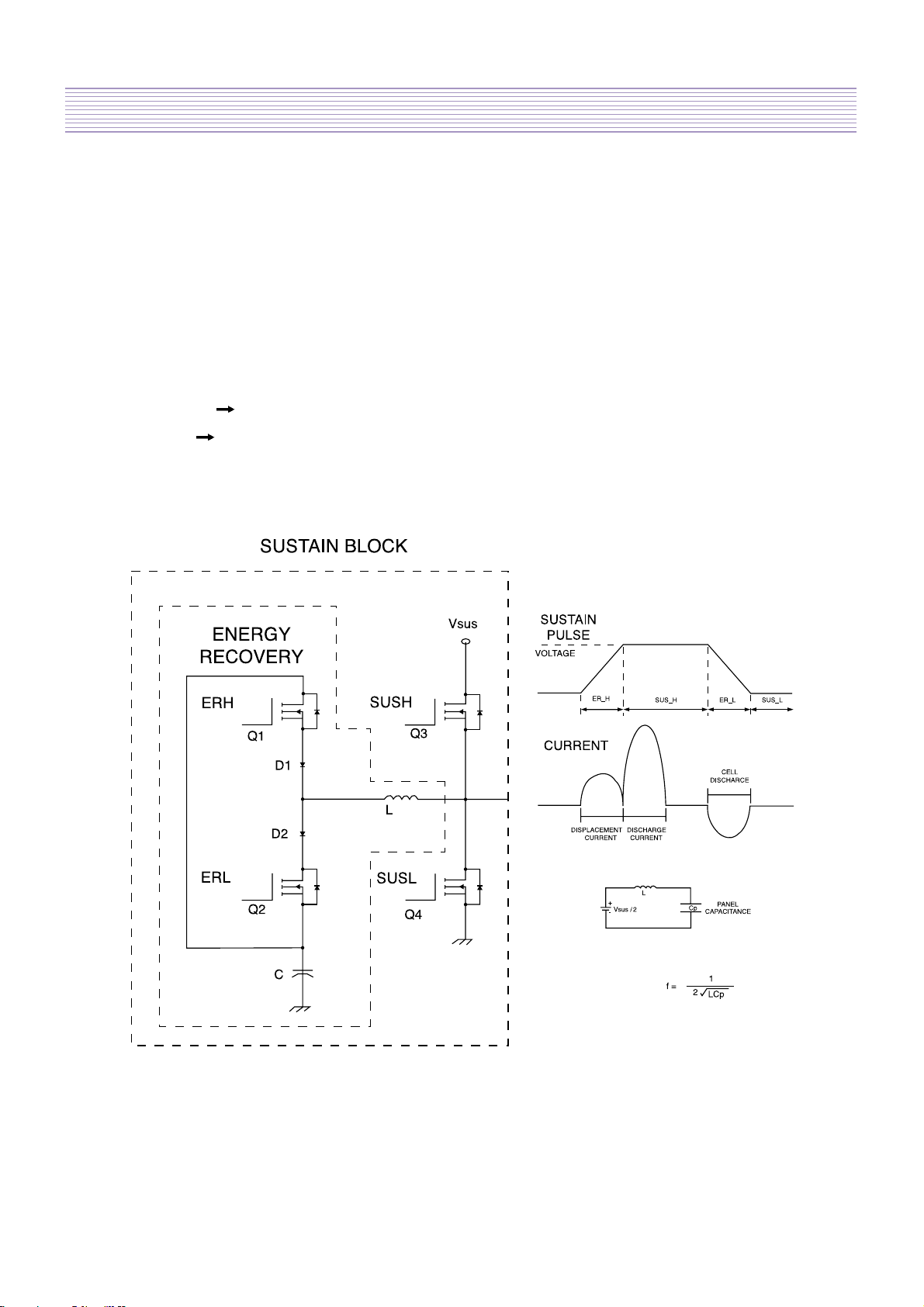
X_SUSTAIN BLOCK SUS_H / SUS_L / ER_H / ER_L(Energy Recovery Circuit)
HIC Structured
Vshelf Generating Circuit From Vsus(173V) to X_HIGHT(163V) voltage generating circuit
15V to X_ N_SHELF(5V) voltage generating circuit Control Voltage by Variable Resistor
RU1
LOGIC Circuit that processes various waveform timing signal
-26-
Description Of Each BLOCK
3) Power Supply
Vsus - Supplied by POWER MODULE. Supplies X-SUS as well as generates X-HIGHT
voltage.(173V)
15V - Supplied by POWER MODULE. Supplies FET driving power as well as generates
X_N_SHELF voltage(5V).
5V - Supplied through CONNECTION-board from DIGITAL-board. Used for LOGIC IC Power.
4) Signal
X_SUSTAIN SUS_H / SUS_L / ER_H / ER_L (Supplied from P202A)
X_SHELF X_N_SHELF / X_HIGHT (Supplied from P202A)
5) SUSTAIN BLOCK
LESONANCE COIL
LESONANCE FREQUENCY
-27-
Description Of Each BLOCK
4-2-5. Y-SUS & SCAN PCB
1) Y_SUSTAIN PCB block diagram
P101A P103A P102A
15V GND GND GND
Y_erase
Remp
_up
&s/w
Y_scan
Scan
(PY1,4)
Scan
(PY1,4)
Scan
(PY4)
Scan
(PY1)
IY8/IY27
_Vcc
Remp
_down
&s/w
shelf
GNDNC
Y_
ERASEV_SUSV_SUS
7
1
11
1
5V
GND
GND
Y_
ERL
Y_
ERH
Y_
SUSL
Y_
SUSH
GND
15V_Y2
15V_Y2
5V_Y2
15V_Y3
15V_Y2
5V_Y3 5V_Y3
5V_Y2
5V_Y2
Y
_ramp_
down
DC-DC
Y_ramp
_up
Y
_ramp
_up
Y_sustain
Ramp_up
S/W
DC-DC
Y_shelf
Y_shelf
DC-DC
Y_scan
PY1 PY2
SCAN-BOARD
Y_ELECTRODES
PY3 PY4
Y_scan
Ramp_down
S/W
Y_erase
15V_Y2
-28-
Description Of Each BLOCK
2) Y_SUSTAIN PCB Structure
SUSTAIN BLOCK SUS_H / SUS_L / ER_H / ER_L (Energy Recovery Circuit)
Structured with HIC
RAMP_UP , RAMP_DOWN waveform generating circuit
RAMP_UP_S/W , RAMP_DOWN_S/W
Y_SCAN -62V(based on GND) Applying Circuit
Y_SHELF 70V(based on GND) Applying Circuit
Yer 166V Applying Circuit
RAMP_UP / Y_SCAN_VH / DC-DC converter circuit that generating Y_SCAN_GND s
voltage
LOGIC Circuit that processes various waveform timing signal
3) Power Supply
Vsus - Supplied from POWER MODULE.(173V)
15V - Supplied from POWER MODULE and used for FET s driving power and input powers of 3
DC-DC converter. Also, generates output voltage of each Y-RAMP_UP / Y-SCAN /
Y_SHELF(Y_SCAN_GND).
5V - Supplied from POWER MODULE through DIGITAL-board. Used for LOGIC IC power
supply. Also, power supply of 5V_Y2, 5V_Y3 is supplied through 7805 regulator from DC-
DC converter Trans TY2 s output.
Yer - Supplied by POWER MODULE. (166V)
GND - Power supply GND / Y1 / Y2 / Y3
4) Signal
Y_SUSTAIN SUS_H / SUS_L / ER_H / ER_L(supplied by P102A)
Y_ERASE (supplied by P103A)
Y_SCAN (supplied by P103A)
Y_RAMP_DOWN & S/W (supplied by P103A)
Y_RAMP_UP & S/W (supplied by P103A)
SCAN CLK / SI1 / SI2 / BLK (supplied by P103A)
-29-
Description Of Each BLOCK
4-2-6. CONNECTION PCB & DATA COF
1) Structure of CONNECTION PCB
Divided into 2 PCBs (CONN-LEFT & CONN-RIGHT)
CONN-LEFT From DIGITAL PCB through connector P304, data signal and 5V IC Power
are supplied. Vadd Power is supplied to PC 5~7 through PC08A.
CONN-RIGHT From DIGITAL PCB through connector P304A, data signal and 5V IC
Power are supplied. 5V Power is supplied to X-board through P202. Also, Data signals are
supplied from DIGITAL PCB through P302A and X-sustain/X-shelf signals are supplied from
X-SUS PCB through P202. Vadd Power is supplied to PC 1~4 from X-SUS PCB through P202
and to CONN-LEFT through PC8A1 and PC08A.
2) Structure of DATA COF
7 COF Type module(PC 1~7)
DATA signals are transferred to CONNECTION PCB from DIGITAL PCB through P304A /
P303A / P302A. And through PC 1~7 each are transferred to DATA COF.
5V supplied from DIGITAL PCB through connector P304A / P303A. Vadd flows POWER PCB
X-SUS PCB connector P202 CONNECTION PCB DATA COF.
-30-
Description Of Each BLOCK
4-3. POWER BLOCK
4-3-1. POWER BLOCK DIAGRAM
Line
ST- BY
PFC
ST- BY
Protection
r
Vyer
Vsus
Vsus
Discharge
5V out
12V out
30V out
15V out
5V out
3.3V out
Vadd
Vadd
IC B+
Main B+
IC ON/OFF
IC B+
Main B+
POWER
ON/OFF
Control
Sequence
Control
Block
B+ 15V
Vlow
AC Input
5V
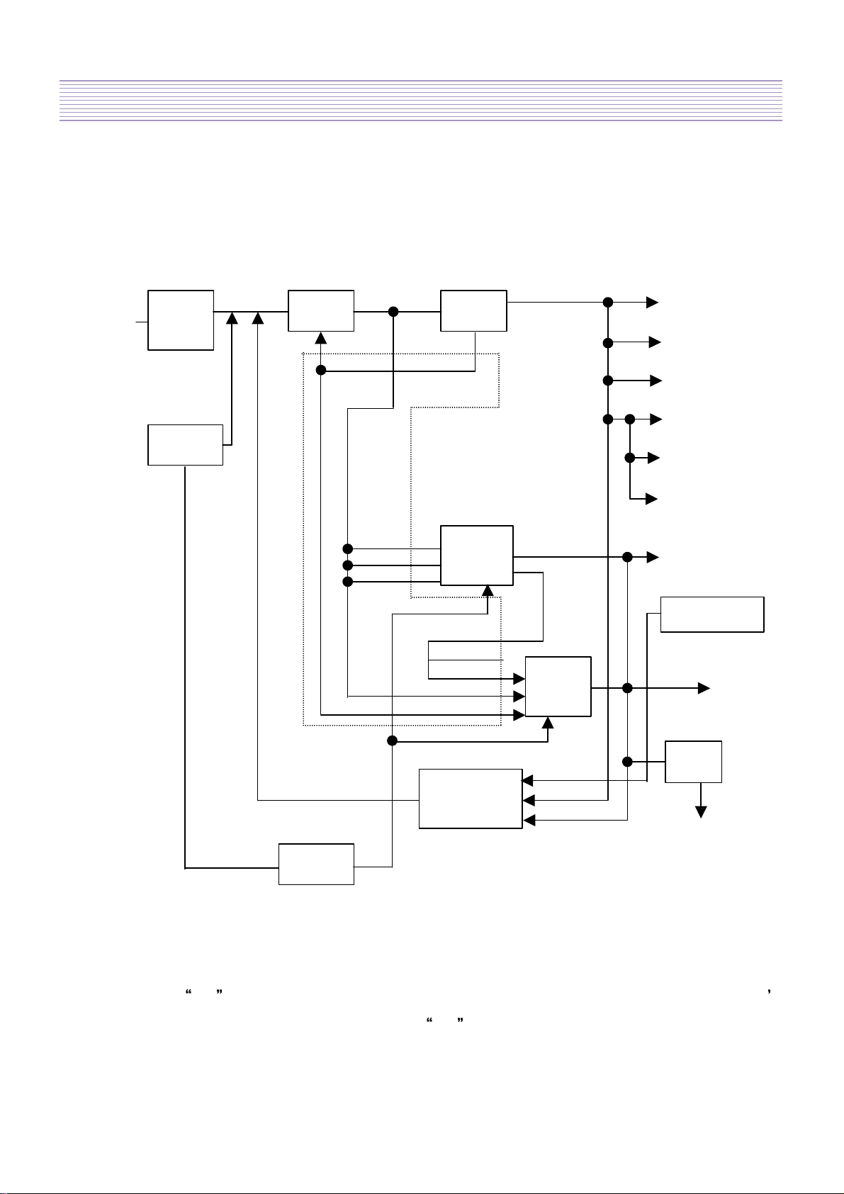
If Power is ON , V_PFC and V_LOW BLOCK is working and Voltage generated in V_LOW s
2nd Coil actuates V_ADD. After V_ADD is
ON , 2nd Voltage generated in V_ADD BLOCK
acutates V_SUS BLOCK again.
Main B+
IC ON/OFF
Vye
 Loading...