

Page 1

http : //svc.dwe.co.kr
Caution
: In this Manual, some parts can be changed for improving. their
performance without notice in the parts list. So, if you need the
latest parts information, please refer to PPL(Parts Price List)in
Service Information Center(http://svc.dwe.co.kr)
DAEWOO ELECTRONICS Corp.
Service Manual
Jan. 2005
COLOR TELEVISION
CHASSIS : CP-093/F
MODEL : DTD-21H9
DTD-14H9
SM No :TCP093FEF0
Page 2

CP-093/F Service Manual
CONTENTS
1. MAIN FEATURES 2
1.1 SPECIFICATIONS 2
1.1.1 GENERAL 2
1.1.2 EURO-SCART 1(21Pin) 3
1.1.3 CHANNEL/FREQUENCY TABLE 4
2. SAFETY INSTRUCTION 7
3. ALIGNMENT INSTRUCTIONS 8
3.1 MICROCONTROLLER CONFIGURATION:SERVICE MODE 8
3.2 SERVICE MODE NADVIGATION 8
3.3 MICROCONTROLLER CONFIGURATION:OPTION BITS 8
3.4 OPTION 1 9
3.5 OPTION 2 9
3.6 NVM default setting 10
4. TV SET ALIGNMENT 12
4.1 G2 ALIGNMENT 12
4.2 WHITE BALANCE 12
4.3 FOCUS 12
4.4 VERTICAL GEOMETRY 12
4.5 HORIZONTAL PICTURE CENTRING 12
4.6 EAST/WEST CORRECTION 12
4.7 AGC 13
5 IC DESCRIPTION 14
5.1 UOC
///
Series 14
5.1.1 IC MARKING AND VERSION 14
5.1.2 BLOCK DIAGRAM 15
5.1.3 PINNING 16
5.1.4 FEATURES 17
5.2 TDA8944J STEREO AUDIO AMPLIFIER 22
5.2.1 FEATURES 23
5.3 TDA8357J VERTICAL AMPLIFIER 25
5.3.1 TDA8357J 25
5.4 TDA6107AJE 28
5.4.1 Features 28
5.4.2 Pin description 28
5.5 24WC16-16KB EEPROM 29
5.6 STR-F6756/4 30
5..6.1 Functions of Each Terminal 30
5..6.2 Block Diagram(Connection diagram) 30
5..6.3 CONTROL PART - ELECTRICAL CHARACTERISTICS 33
6. SPECIFICATIONS 34
7. SERVICE PARTS LIST 37
8. EXPLODED VIEW 51
9. PRINTED CIRCUIT BOARD 53
10. SCHEMATIC DIAGRAM 55
Page 3
1. MAIN FEATURES
2
1.1 SPECIFICATIONS
1.1.1 GENERAL
TV standard PAL - SECAM B/G D/K, PAL I/I, SECAM L/L’
Sound system NICAM B/G, I, D/K, L,
Power
consumption
Sound Output
Power
Speaker 14” : 3W 8 ohm x 2 (No sound when AV2 PCB
Teletext system 10 pages memory FASTEXT (FLOF or TOP)
Aerial input 75 ohm unbalanced
Channel coverage Off-air channels, S-cable channels and hyperband
Tuning system frequency synthesiser tuning system
Visual screen size 14” : 33cm
Channel indication On Screen Display
Program Selection 100 programmes
Aux. terminal - EURO-SCART : Audio / Video In and Out, R/G/B
Remote Control
Unit
CP-093/F Service Manual
Tuner PAL, SECAMColour system
AV PAL, SECAM, PAL 60, NTSC M, NTSC 4.43
FM 2Carrier B/G, D/K
14” : 66W
21” : 74W
14” : 1.5W x 2 (at 60% mod, 10% THD)
20” : 3W x 2 (at 60% mod, 10%THD)
21” : 5W 8 ohm x2 is not connected)
21” : 51cm
In, Slow and Fast switching.
-SPDIF and Audio L/R out at back of cabinet.
(14”)
- Headphone jack on front of cabinet
(21”)
- AV2 : Video and Audio L/R out, Headphone jack
at side of cabinet.
R-52C03
Page 4
CP-093/F Service Manual
3
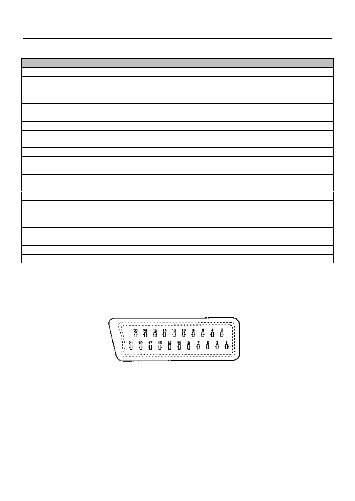
1.1.2 EURO-SCART 1 (21 Pin)
Pin Signal Description Matching value
1 Audio Output Right 0.5 Vrms, Impedance < 1 kΩ, ( RF 54% Mod )
2 Audio Input Right 0.5 Vrms, Impedance > 10 kΩ
3 Audio Output Left 0.5 Vrms, Impedance < 1 kΩ, ( RF 54% Mod )
4 Audio Earth
5 Blue Earth
6 Audio Input Left 0.5 Vrms, Impedance > 10 kΩ
7 Blue Input 0.7 Vpp ±0.1V, Impedance 75Ω
8 Slow Switching TV : 0 to 2V, AV 16/9 : 4.5 to 7V, AV 4/3 : 9.5 to 12V , Impedance
> 10 kΩ
9 Green Earth
10 N.C.
11 Green Input 0.7 Vpp ± 0.1V, Impedance 75Ω
12 N.C.
13 Red Earth
14 Blanking Earth
15 Red Input
16 Fast Switching 0 to 0.4V : Logic “0”, 1 to 3V : Logic “1”, Impedance 75Ω
17 Video Out Earth
18 Video In Earth
19 Video Output
20 Video Input 1 Vpp ± 3dB, Impedance 75Ω
21 Common Earth
0.7 Vpp ± 0.1V, Impedance 75Ω
1 Vpp ± 3dB, Impedance 75Ω
Page 5

CP-093/F Service Manual
4
1.2 CHANNEL/FREQUENCY TABLE
CHANNEL EUROPE CCIR FRANCE GB(IRELAND) EAST OIRT
C01
C02
C03
C04
C05
C06
C07
C08
C09
C10
C11
C12
C13
C14
C15
C16
C17
C18
C19
C20
C21
C22
C23
C24
C25
C26
C27
C28
C29
C30
C31
C32
C33
C34
C35
C36
C37
C38
C39
C40
C41
C42
C43
C44
C45
46.25 - 45.75 49.75
48.25 55.75 (L') 53.75 59.25
55.25 60.5 (L') 61.75 77.25
62.25 63.75 (L') 175.25 85.25
175.25 176.00 183.25 93.25
182.25 184.00 191.25 175.25
189.25 192.00 199.25 183.25
196.25 200.00 207.25 191.25
203.25 208.00 215.25 199.25
210.25 216.00 223.25 207.25
217.25 189.25 (LUX) 231.25 215.25
224.25 69.25 (L') 239.25 223.25
53.75 76.25 (L') 247.25 -
- 83.25 (L') 49.75 -
82.25 90.25 57.75 -
- 97.25 65.75 -
183.75 - 77.75 -
192.25 - 85.75 -
201.25 - - -
- - - -
471.25 471.25 471.25 471.25
479.25 479.25 479.25 479.25
487.25 487.25 487.25 487.25
495.25 495.25 495.25 495.25
503.25 503.25 503.25 503.25
511.25 511.25 511.25 511.25
519.25 519.25 519.25 519.25
527.25 527.25 527.25 527.25
535.25 535.25 535.25 535.25
543.25 543.25 543.25 543.25
551.25 551.25 551.25 551.25
559.25 559.25 559.25 559.25
567.25 567.25 567.25 567.25
575.25 575.25 575.25 575.25
583.25 583.25 583.25 583.25
591.25 591.25 591.25 591.25
599.25 599.25 599.25 599.25
607.25 607.25 607.25 607.25
615.25 615.25 615.25 615.25
623.25 623.25 623.25 623.25
631.25 631.25 631.25 631.25
639.25 639.25 639.25 639.25
647.25 647.25 647.25 647.25
655.25 655.25 655.25 655.25
663.25 663.25 663.25 663.25
Page 6

CP-093/F Service Manual
5
C46
C47
C48
C49
C50
C51
C52
C53
C54
C55
C56
C57
C58
C59
C60
C61
C62
C63
C64
C65
C66
C67
C68
C69
C70
C71
C72
C73
C74
C75
C76
C77
S01
S02
S03
S04
S05
S06
S07
S08
S09
S10
S11
S12
S13
S14
S15
S16
S17
671.25 671.25 671.25 671.25
679.25 679.25 679.25 679.25
687.25 687.25 687.25 687.25
695.25 695.25 695.25 695.25
703.25 703.25 703.25 703.25
711.25 711.25 711.25 711.25
719.25 719.25 719.25 719.25
727.25 727.25 727.25 727.25
735.25 735.25 735.25 735.25
743.25 743.25 743.25 743.25
751.25 751.25 751.25 751.25
759.25 759.25 759.25 759.25
767.25 767.25 767.25 767.25
775.25 775.25 775.25 775.25
783.25 783.25 783.25 783.25
791.25 791.25 791.25 791.25
799.25 799.25 799.25 799.25
807.25 807.25 807.25 807.25
815.25 815.25 815.25 815.25
823.25 823.25 823.25 823.25
831.25 831.25 831.25 831.25
839.25 839.25 839.25 839.25
847.25 847.25 847.25 847.25
855.25 855.25 855.25 855.25
863.25 863.25 863.25 863.25
69.25 - - -
76.25 - - -
83.25 - - -
90.25 - - -
97.25 - - -
59.25 - - -
93.25 - - -
105.25 104.75 103.25 105.25
112.25 116.75 111.25 112.25
119.25 128.75 119.25 119.25
126.25 140.75 127.25 126.25
133.25 152.75 135.25 133.25
140.25 164.75 143.25 140.25
147.25 176.75 151.25 147.25
154.25 188.75 159.25 154.25
161.25 200.75 167.25 161.25
168.25 212.75 - 168.25
231.25 224.75 - 231.25
238.25 236.75 - 238.25
245.25 248.75 255.25 245.25
252.25 260.75 263.25 252.25
259.25 272.75 271.25 259.25
266.25 284.75 279.25 266.25
273.25 296.75 287.25 273.25
Page 7

CP-093/F Service Manual
6
S18
S19
S20
S21
S22
S23
S24
S25
S26
S27
S28
S29
S30
S31
S32
S33
S34
S35
S36
S37
S38
S39
S40
S41
280.25 136.00 295.25 280.25
287.25 160.00 303.25 287.25
294.25 - - 294.25
303.25 303.25 - 303.25
311.25 311.25 311.25 311.25
319.25 319.25 319.25 319.25
327.25 327.25 327.25 327.25
335.25 335.25 335.25 335.25
343.25 343.25 343.25 343.25
351.25 351.25 351.25 351.25
359.25 359.25 359.25 359.25
367.25 367.25 367.25 367.25
375.25 375.25 375.25 375.25
383.25 383.25 383.25 383.25
391.25 391.25 391.25 391.25
399.25 399.25 399.25 399.25
407.25 407.25 407.25 407.25
415.25 415.25 415.25 415.25
423.25 423.25 423.25 423.25
431.25 431.25 431.25 431.25
439.25 439.25 439.25 439.25
447.25 447.25 447.25 447.25
455.25 455.25 455.25 455.25
463.25 463.25 463.25 463.25
Page 8

CP-093/F Service Manual
7
2. SAFETY INSTRUCTION
WARNING: Only competent service personnel may carry out work involving the testing or repair
of this equipment.
X-RAY RADIATION PRECAUTION
1. Excessive high voltage can produce potentially hazardous X-RAY RADIATION. To avoid
such hazards, the high voltage must not exceed the specified limit. The nominal value of the high
voltage of this receiver is 25-26 KV (20 ”-21”) or 26 KV (25” - 28 ”) at max beam current. The high
voltage must not, under any circumstances, exceed 27.5 KV (20 ”), 29KV (21”), 29.5 KV (25") or
30 KV (28"). Each time a receiver requires servicing, the high voltage should be checked. It is
important to use an accurate and reliable high voltage meter.
2. The only source of X-RAY Radiation in this TV receiver is the picture tube. For continued
X-RAY RADIATION protection, the replacement tube must be exactly the same type tube as
specified in the parts list.
SAFETY PRECAUTION
Potentials of high voltage are present when this receiver is operating. Operation of the receiver
outside the cabinet or with the back board removed involves a shock hazard from the receiver.
Servicing should not be attempted by anyone who is not thoroughly familiar with the precautions
necessary when working on high voltage equipment.
Discharge the high potential of the picture tube before handling the tube. The picture tube is
highly evacuated and if broken, glass fragments will be violently expelled.
If any Fuse in this TV receiver is blown, replace it with the FUSE specified in the Replacement
Parts List.
When replacing a high wattage resistor (metal oxide film resistor) in the circuit board, keep the
resistor 10 mm away from circuit board.
Keep wires away from high voltage or high temperature components.
This receiver must operate under AC 230 volts, 50 Hz. NEVER connect to a DC supply or any
other voltage or frequency.
PRODUCT SAFETY NOTICE
Many electrical and mechanical parts in this equipment have special safety-related
characteristics. These characteristics are often passed unnoticed by a visual inspection and the
X-RAY RADIATION protection afforded by them cannot necessarily be obtained by using
replacement components rated for higher voltage, wattage, etc. Replacement parts which have
these special safety characteristics are identified in this manual and its supplements, electrical
components having such features are identified by designated symbol on the parts list. Before
replacing any of these components, read the parts list in this manual carefully. The use of
substitutes replacement parts which do not have the same safety characteristics as specified in
the parts list may create X-RAY Radiation.
Page 9

CP-093/F Service Manual
8
3. ALIGNMENT INSTRUCTIONS
3.1 MICROCONTROLLER CONFIGURATION : SERVICE MODE
To switch the TV set into service mode please see instruction below.
1 - Select PR. number 91
2 - Adjust sharpness to minimum and exit all menus.
3 – Within 2 seconds press the key sequence : RED - GREEN - menu
The software version is displayed beside the word Service, e.g. “SERVICE VER 00.05”.
To exit SERVICE menu press menu key or Std By key.
3.2 SERVICE MODE NAVIGATION
Pr Up/Down remote keys : cycle through the service items available.
Vol -/+ remote keys : Dec./Increment the values within range – Cycle trough option bits.
OK key : Toggle bits in option byte
Order Item Default setting
1 HOR CEN
2 RED GAIN
3 GRN GAIN
4 BLUE GAIN
5 RED BIAS
6 GRN BIAS
7 AGC LEVEL
8 G2 – SCREEN
9 OPTION1
10 OPTION2
11 AVL
12 PARABOLA
13 HOR WIDTH
14 CORNER T
15 CORNER B
16 HOR. PARAL
17 V. LINEAR
18 V. SLOPE
19 EW TRAPEZ
20 S CORRECT
21 VERT CENT
22 VERT SIZE
3.3 MICROCONTROLLER CONFIGURATION : OPTION BITS
There are two option bytes available (16 bits in all). These option bits are available from Service
mode. First find the OPTION1 or OPTION2 control, and then use the Volume PLUS/MINUS
buttons on the remote control keypad to locate the bits, and OK key to toggle them. The table
below shows the two option bytes available;
Page 10

3.4 OPTION 1
9
B7 B6 B5 B4 B3 B2 B1 B0
TOP
1
Teletext
OFF
TOP
Teletext
0
ON
3.5 OPTION 2
B7 B6 B5 B4 B3 B2 B1 B0
1
Fixed to
‘0’
0
FASTEXT
(FLOF)
OFF
FASTEXT
(FLOF) ON
JVC
remote
control
Daewoo
Remote
control
TUBE
4:3
TUBE
16:9
AVL
control
OFF
AVL
control
ON
VAI bit set
to 1 in
SECAM L
VAI bit set
to 0 in
SECAM L
PICTURE
TILT ON
PICTURE
TILT OFF
Dolby
Virtual
OFF
Dolby
Virtual
ON
14”
(AV2
OFF)
21”
(AV2
ON)
SVHS3
disable
SVHS3
enable
Full
ATSS
Basic
ATSS
CP-093/F Service Manual
TUNER OPTIONS
00 = Philips
01 = Not used
10 = Alps
11 = Parstnic (DW)
Double
Window
Enabled
Double
Window
Disabled
n.u.
Must
be set
to 1 for
future
compa
tibility
Page 11

CP-093/F Service Manual
10
3.6 NVM default setting
The purpose of this message, when you change a virgin EEPROM, is to allow to modify
the NVM DATA to desired values.
1 - Introduction :
The NVM default values are fixed for the user, but for flexibility in service, these data are stored
in NVM and can be changed when the TV set is in a special mode call "NVM EDITOR". This
mode can only be access from "FACTORY" mode.
2 - Entering into "FACTORY" mode.
To switch the TV set into FACTORY mode, use the factory remote control, and press on “SVC”
key. The factory menu will appear on the screen, showing “FACTORY” , plus other relevant
information like software version and date.
WARNING : When in "FACTORY" mode you should not press any key other than the keys
described in the procedure below. Unwanted key stroke could misadjust the TV set.
3 - Entering into "NVM EDITOR" mode.
To switch the TV set into NVM EDITOR mode, use the user remote control, and press on
“ON/ENTER” key. The NVM EDITOR window will appear on the screen. This mode allow you to
access all data stored in NVM. The current NVM address is given in column "ADDR." in both
DECimal and HEXadecimal format. The column DATA gives the value contained at selected
address in both DECimal and HEXadecimal format.
4 - Navigation in "NVM EDITOR" mode.
Use Program Up/Dwn keys to select the desired address. Use Volume Up/Down keys to change
the data at selected address. You must press " OK/ENTER" key to store value after modification.
The data can be adjusted between 0 and 63.
5 - Exit "NVM EDITOR" mode.
To switch the TV set back into FACTORY mode, use the user remote control, and press on
“MENU” key.
The factory menu will appear on the screen, showing “FACTORY”.
6 - Exit "FACTORY" mode.
To exit "FACTORY" mode, use the factory remote control, and press on “SVC” key.
The factory menu will disappear from the screen.
Page 12

CP-093/F Service Manual
11
NVM DATA CHANGE LIST
No Register Name Address Default 14H9 21H9
1 OCP_THRESHOLD 0x58F 0x91 <- <2 DCXO 0x590 0x4E <- <3 AVLLEV 0x621 0x5 <- <4 TELETEXT - Brightness 0x642 0x19 <- <5 OSD - Brightness 0x644 0x7 <- <6 Nor1_Bright 0x64A 0x23 <- <7 Nor1_contrast 0x64B 0x2E <- <8 Nor1_Colour 0x64C 0x1C <- <9 Nor1_Sharpness 0x64D 0x23 <- <-
10 Nor1_Tint 0x64E 0x20 0x1F 0x1F
11 Nor2_Bright 0x653 0x28 <- <12 Nor2_Contrast 0x654 0x13 <- <13 Nor2_Colour 0x655 0x19 <- <-
14 Nor2_Sharpness 0x656 0x1B <- <15 Nor2_Tint 0x657 0x20 0x1F 0x1F
16 V - Linearity 0x667 0x2A 0x22 0x27
17 Peak White Level 0x671 0x1 <- <18 Soft Clipping Level 0x672 0x5 0x7 0x7
19 PresetGainRGB 0x673 0x2A 0x1 0x7
20 PresetGainRGB 0x674 0x2A 0x1 0x7
(hex)
21 PresetGainRGB 0x675 0x2A 0x1 0x7
22 Cathode_Drive 0x67B 0x1 <- <23 RPA 0x680 0x1 0x2 0x2
24 Black Stretch 0x682 0x1 0x2 0x2
25 BSD 0x683 0x1 0x0 0x0
26 AAS 0x684 0x1 0x0 0x0
27 BCS 0x685 0x1 <- <28 Y_delay_PAL_BG 0x686 0x5 <- <29 Y_delay_SECAM_BG 0x687 0x8 <- <-
30 Y_delay_PAL_DK 0x688 0x5 <- <31 Y_delay_SCM_DK 0x689 0x5 <- <32 Y_delay_PAL_I 0x68A 0x7 <- <33 Y_delay_SECAM 0x68B 0x5 <- <34 Y_delay_SECAM-L 0x68C 0x8 <- <35 Y_delay_AV 0x68D 0xA <- <36 G2_Bright 0x68E 0x1A <- <37 G2_Contrast 0x68F 0x42 <- <-
Page 13
CP-093/F Service Manual
12
4. TV SET ALIGNMENT
4.1 G2 ALIGNMENT
- Tune a colour bar pattern.
- Find the “G2 – SCREEN ” item in service mode.
- Adjust screen volume (on FBT) to bring the cursor to central position (Green).
4.2 WHITE BALANCE
- Select a dark picture and adjust RED BIAS and GRN BIAS to the desired colour temperature.
- Select a bright picture and adjust RED, GRN and BLUE GAIN to the desired colour temperature.
4.3 FOCUS
Adjust the Focus volume (on FBT) to have the best resolution on screen.
4.4 VERTICAL GEOMETRY
Adjust V. LINEAR (linearity), S CORRECT (S. Correction), VERT SIZE (Vertical amplitude),
VERT CENT (vertical centring) to compensate for vertical distortion.
4.5 HORIZONTAL PICTURE CENTRING
Adjust HOR CEN (Horizontal centre) to have the picture in the centre of the screen.
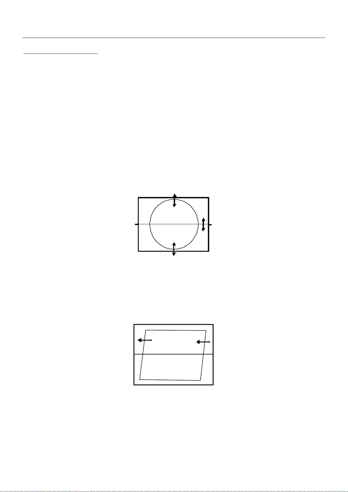
4.6 EAST / WEST CORRECTION
Adjust the PARABOLA, HOR WIDTH, CORNER, HOR PARAL, EW TRAPEZ, to compensate for
geometrical distortion.
HOR PARAL
Page 14
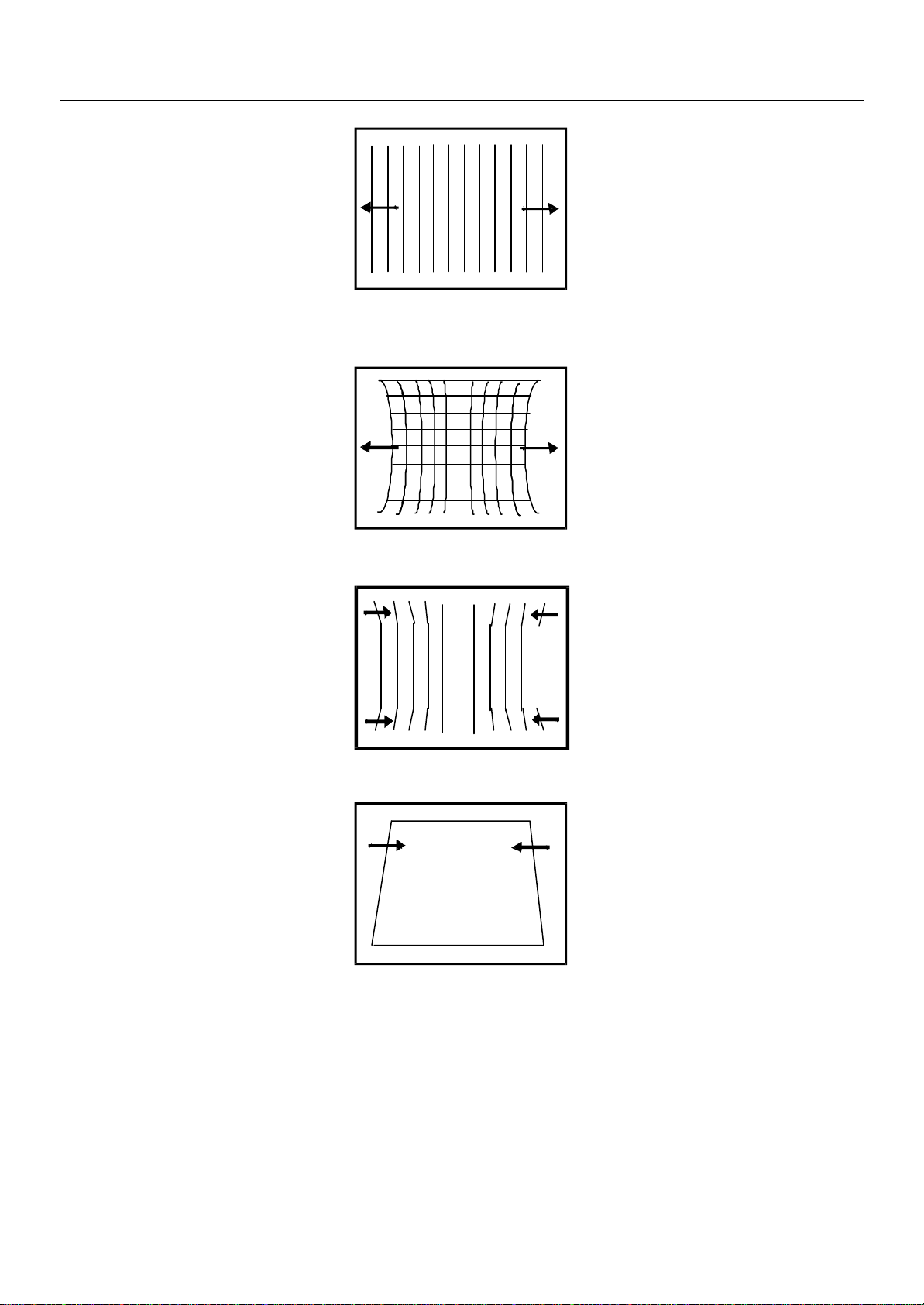
HOR WIDTH
13
adjust for 93% overscan.
CP-093/F Service Manual
PARABOLA
CORNER B & CORNER T
EW TRAPEZ
4.7 AGC
- Make sure option bits are correct for the tuner fitted on the chassis (See above how to change
option bits).
- Adjust the antenna signal level at 62 dBµV
- Tune a colour bar pattern.
- Find the “AGC” item in service mode.
- Press the key “OK ” on the remote keypad and wait until AGC level stabilise to the optimum
value.
Page 15

CP-093/F Service Manual
14
- Alternatively, use “Vol Up/Dwn ” keys to adjust manually to the desired Tuner Take Over Point
(TOP).
5. IC DESCRIPTION
5.1 UOC
The UOC
III
Series
III
series combines the functions of a Video Signal Processor (VSP) together with a
FLASH embedded TEXT/Control/Graphics µ-Controller (TCG µ-Controller) and US Closed
Caption decoder. In addition the following functions can be added:
• Adaptive digital (4H/2H) PAL/NTSC combfilter
• Teletext decoder with 10 page text memory
• Multi-standard stereo decoder
• BTSC stereo decoder
• Digital sound processing circuit
• Digital video processing circuit
5.1.1 IC MARKING AND VERSION
Chassis IC marking OSD languages ATSS countries Text
BULGARIAN,
Austria, Belgium,
Switzerland, Czech
Republic, Germany,
Denmark, Spain,
France, Finland, GB,
Greece, Hungary, Italy,
Ireland, Norway,
Netherlands, Portugal,
Poland, Sweden,
Slovak Republic,
Others
PAN-EUROPEAN
LATIN, CYRILLIC,
GREEK.
CP-093
CP-093F
CZECH, GERMAN,
DANISH, SPANISH,
FRENCH, FINNISH,
ENGLISH, GREEK,
HUNGARIAN,
ITALIAN,
NORWEGIAN,
DUTCH, POLISH,
ROMANIAN,
RUSSIAN,
SWEDISH,
SLOVAKIAN.
Page 16
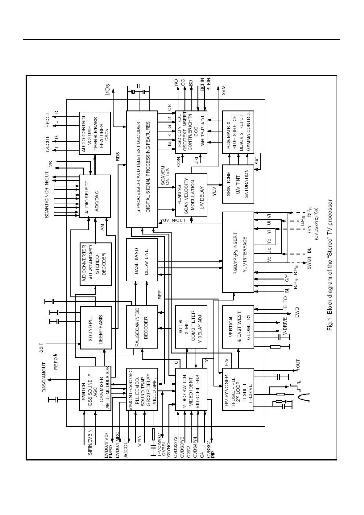
5.1.2. BLOCK DIAGRAM
15
CP-093/F Service Manual
Page 17

CP-093/F Service Manual
16
5.1.3. PINNING
QFP 128pin Symbol Short Description
1 P1.5/TX Port 1.5 or UART bus
2 P1.4/RX port 1.4 or UART bus
3 P1.2/INT2 port 1.2 or external interrupt 2
4 VSSC3 Ground
5 VDDC3 digital supply to core (1.8V)
6 P2.5/PWM4 port 2.5 or PWM4 output
7 P2.4/PWM3 port 2.4 or PWM3 output
8 VSSC/P digital ground for m-Controller core and periphery
9 P3.3/ADC3 port 3.3 or ADC3 input
10 P3.2/ADC2 port 3.2 or ADC2 input
11 DECV1V8 decoupling 1.8 V supply
12 VDDC1 digital supply to core (+1.8 V)
13 P3.1/ADC1 port 3.1 or ADC1 input
14 P3.0/ADC0 port 3.0 or ADC0 input
15 P2.3/PWM2 port 2.3 or PWM2 output
16 P2.2/PWM1 port 2.2 or PWM1 output
17 P2.1/PWM0 port 2.1 or PWM0 output
18 P2.0/TPWM port 2.0 or Tuning PWM output
19 VDDP(3.3V)
20 P1.7/SDA port 1.7 or I2C-bus data line
21 P1.6/SCL port 1.6 or I2C-bus clock line
22 P1.3/T1 port 1.3 or Counter/Timer 1 input
23 P0.0/I2SDI1/O port 0.0 or I2S digital input 1 or I2S digital output
24 P0.1/I2SDO1 port 0.1 or I2S digital output 1
25 P0.2/I2SDO2 port 0.2 or I2S digital output 2
26 P0.3/I2SCLK port 0.3 or I2S clock
27 P0.4/I2SWS port 0.4 or I2S word select
28 VSSC2 Ground
29 VDDC2 digital supply to core (1.8 V)
30 P1.1/T0 port 1.1 or Counter/Timer 0 input
31 P1.0/INT1 port 1.0 or external interrupt 1
32 INT0/P0.5
33 VDDadc(1.8) supply voltage video ADC
34 VSSadc ground for on-chip temperature sensor
35 VDDA2(3.3) supply voltage SDAC (3.3 V)
36 VDDA(1.8) analogue supply for audio ADCs (1.8 V)
37 GNDA Ground
38 VREFAD reference voltage for audio ADCs (3.3/2 V)
39 VREFAD_POS positive reference voltage (3.3 V)
40 VREFAD_NEG negative reference voltage (0 V)
41 VDDA1
42 BO Blue output
43 GO Green output
supply to periphery and on-chip voltage regulator (3.3
V)
external interrupt 0 or port 0.5 (4 mA current sinking
capability for direct drive of LEDs)
analog supply for TCG m-Controller and digital supply
for
TV-processor (+3.3 V)
Page 18

CP-093/F Service Manual
17
44 RO Red output
45 BLKIN black current input
46 BCLIN beam current limiter input
47 VP3 3rd supply for TV processor
48 GND3 ground 3 for TV-processor
49 B/PBIN3 3rd B input / PB input
50 G/YIN3 3rd G input / Y input
51 R/PRIN3 3rd R input / PR input
52 INSSW3 3rd RGB / YPBPR insertion input
53 VOUT(SWO1)
54 UOUT(INSSW2)
55 YOUT Y-output (for YUV interface)
56 YSYNC Y-input for sync separator
57 YIN (G/YIN2/CVBS-Yx)
58 UIN (B/PBIN2) U-input for YUV interface (2nd B input / PB input)
59 VIN (R/PRIN2/CX)
60 VDDcomb supply voltage for comb filter (5 V)
61 VSScomb ground connection for comb filter
62 HOUT horizontal output
63 FBISO/CSY
64 SVM scan velocity modulation output
65 CVBSO/PIP CVBS / PIP output
66 AUDOUTHPR audio output for headphone channel (right signal)
67 AUDOUTHPL audio output for headphone channel (left signal)
68 AUDOUTLSR audio output for audio power amplifier (right signal)
69 AUDOUTLSL audio output for audio power amplifier (left signal)
70 C2/C3 chroma-2/3 input
71 CVBS3/Y3 CVBS3/Y3 input
72 AUDIOIN3R audio 3 input (right signal)
73 AUDIOIN3L audio 3 input (left signal)
74 CVBS2/Y2 CVBS2/Y2 input
75 AUDIOIN2R audio 2 input (right signal)
76 AUDIOIN2L audio 2 input (left signal)
77 C4 chroma-4 input
78 CVBS4/Y4 CVBS4/Y4 input
79 AUDIOIN4R audio-4 input (right signal)
80 AUDIOIN4L audio-4 input (left signal)
81 IFVO/SVO/CVBSI (2) IF video output / selected CVBS output / CVBS input
82 VP2 2nd supply voltage TV processor (+5 V)
83 AGC2SIF AGC capacitor second sound IF
84 VCC8V 8 Volt supply for audio switches
85 DVBO/FMRO (2) Digital Video Broadcast output / FM radio output
86 DVBO/IFVO/FMRO (2)
V-output for YUV interface (general purpose switch
output)
U-output for YUV interface (2nd RGB / YPBPR
insertion input)
Y-input for YUV interface (2nd G input / Y input or
CVBS/YX input))
V-input for YUV interface (2nd R input / PR input or CX
input)
flyback input/sandcastle output or composite H/V
timing output
Digital Video Broadcast output / IF video output / FM
radio output
Page 19

CP-093/F Service Manual
18
87 SIFAGC/DVBAGC (2)
88 PLLIF IF-PLL loop filter
89 GND2 ground 2 for TV processor
90
91 DECSDEM decoupling sound demodulator
92 AUDOUTSR audio output for SCART/CINCH (right signal)
93 AUDOUTSL audio output for SCART/CINCH (left signal)
94 AUDIOIN5R audio-5 input (right signal)
95 AUDIOIN5L audio-5 input (left signal)
96
97 EHTO EHT/overvoltage protection input
98 AGCOUT tuner AGC output
99 SIFIN2/DVBIN2 (2) SIF input 2 / DVB input 2
100 SIFIN1/DVBIN1 (2) SIF input 1 / DVB input 1
101 GNDIF ground connection for IF amplifier
102 IREF reference current input
103 VSC vertical sawtooth capacitor
104 VIFIN2 IF input 2
105 VIFIN1 IF input 1
106 VDRA vertical drive A output
107 VDRB vertical drive B output
108 EWD/AVL (1) East-West drive output or AVL capacitor
109 DECBG bandgap decoupling
110 SECPLL SECAM PLL decoupling
111 GND1 ground 1 for TV-processor
112 PH1LF phase-1 filter
113 PH2LF phase-2 filter
114 VP1 1st supply voltage TV-processor (+5 V)
115 DECDIG decoupling digital supply
116 VGUARD/SWIO
117 VSSA1 Ground
118 XTALOUT crystal oscillator output
119 XTALIN crystal oscillator input
120 VREF_POS_HPR positive reference voltage SDAC (3.3 V)
121 VREF_NEG_HPL+HPR negative reference voltage SDAC (0 V)
122 VREF_POS_LSR+HPR positive reference voltage SDAC (3.3 V)
123 VREF_NEG_LSL+HPL negative reference voltage SDAC (0 V)
124 VREF_POS_LSL positive reference voltage SDAC (3.3 V)
125 VDDA3(3.3V) supply (3.3 V)
126 VDDC4 digital supply to SDACs (1.8V)
127 VSSC4 Ground
128 VSSP2 Ground
QSSO/AMOUT/AUDEE
M (2)
AVL/SWO/SSIF/
REFO/REFIN (2)
AGC sound IF / internal-external AGC for DVB
applications
QSS intercarrier output / AM output / deemphasis
(front-end audio out)
Automatic Volume Levelling / switch output / sound IF
input /
subcarrier reference output / external reference signal
input for I
signal mixer for DVB operation
V-guard input / I/O switch (e.g. 4 mA current sinking
capability for
direct drive of LEDs)
Page 20

CP-093/F Service Manual
19
5.1.4 FEATURES
Analogue Video Processing (all versions)
· Multi-standard vision IF circuit with alignment-free PLL demodulator
· Internal (switchable) time-constant for the IF-AGC circuit
· Switchable group delay correction and sound trap (with switchable centre frequency) for the
demodulated CVBS signal
· DVB/VSB IF circuit for preprocessing of digital TV signals.
· Video switch with 3 external CVBS inputs and a CVBS output. All CVBS inputs can be used as
Y-input for Y/C signals. However, only 2 Y/C sources can be selected because the circuit has 2
chroma inputs. It is possible to add an additional CVBS(Y)/C input (CVBS/YX and CX) when the
YUV interface and the RGB/YPRPB input are not needed.
· Automatic Y/C signal detector
· Adaptive digital (4H/2H) PAL/NTSC comb filter for optimum separation of the luminance and the
chrominance signal.
· Integrated luminance delay line with adjustable delay time
· Picture improvement features with peaking (with switchable centre frequency, depeaking,
variable positive/negative peak ratio, variable pre-/overshoot ratio and video dependent coring),
dynamic skin tone control, gamma control and blue- and black stretching. All features are
available for CVBS, Y/C and RGB/YPBPR signals.
· Switchable DC transfer ratio for the luminance signal
· Only one reference (24.576 MHz) crystal required for the TCG m-Controller, digital sound
processor, Teletext and the colour decoder
· Multi-standard colour decoder with automatic search system and various “forced mode”
possibilities
· Internal base-band delay line
· Indication of the Signal-to-Noise ratio of the incoming CVBS signal
· Linear RGB/YPBPR input with fast insertion.
· YUV interface. When this feature is not required some pins can be used as additional
RGB/YPBPR input. It is also possible to use these pins for additional CVBS (or Y/C) input
(CVBS/YX and CX).
· Tint control for external RGB/YPBPR signals
· Scan Velocity Modulation output. The SVM circuit is active for all the incoming CVBS, Y/C and
RGB/YPBPR signals. The SVM function can also be used during the display of teletext pages.
· RGB control circuit with ‘Continuous Cathode Calibration’, white point and black level off-set
adjustment so that the colour temperature of the dark and the light parts of the screen can be
chosen independently.
· Contrast reduction possibility during mixed-mode of OSD and Text signals
· Adjustable ‘wide blanking ’ of the RGB outputs
· Horizontal synchronization with two control loops and alignment-free horizontal oscillator
· Vertical count-down circuit
· Vertical driver optimized for DC-coupled vertical output stages
· Horizontal and vertical geometry processing with horizontal parallelogram and bow correction
and horizontal and vertical zoom
· Low-power start-up of the horizontal drive circuit
Analogue video processing (stereo versions)
· The low-pass filtered ‘mixed down’ I signal is available via a single ended or balanced output
stage.
Analogue video processing (mono versions)
· The low-pass filtered ‘mixed down’ I signal is available via a single ended output stage
Digital Video Processing (some versions)
· Double Window mode applications. It is possible to display a video and a text window or 2 text
Page 21

CP-093/F Service Manual
20
windows in parallel.
· Linear and non-linear horizontal scaling of the video signal to be displayed.
Sound Demodulation (all versions)
· Separate SIF (Sound IF) input for single reference QSS (Quasi Split Sound) demodulation.
· AM demodulator without extra reference circuit
· The mono intercarrier sound circuit has a selective FM-PLL demodulator which can be switched
to the different FM sound frequencies (4.5/5.5/6.0/6.5 MHz). The quality of this system is such
that the external band-pass filters can be omitted. In the stereo versions of UOCIII the use of this
demodulator is optional for special applications. Normally the FM demodulators of the stereo
demodulator/decoder part are used (see below).
· The FM-PLL demodulator can be set to centre frequencies of 4.72/5.74 MHz so that a second
sound channel can be demodulated. In such an application it is necessary that an external
bandpass filter is inserted.
· The vision IF and mono intercarrier sound circuit can be used for the demodulation of FM radio
signals. With an external FM tuner also signals with an IF frequency of 10.7 MHz can be
demodulated.
· Switch to select between 2nd SIF from QSS demodulation or external FM (SSIF)
Audio Interfaces and switching (stereo versions with Audio DSP)
· Audio switch circuit with 4 stereo inputs, a stereo output for SCART/CINCH, 1 stereo output for
HEADPHONE. The headphone channel has an analogue volume control circuit for the L and R
channel. Finally 1 stereo SPEAKER output with digital controls.
· AVL (Automatic Volume Levelling) circuit for the headphone channel.
· Digital input crossbar switch for all digital signal sources and destinations
· Digital output crossbar for exchange of channel processing functionality
· Digital audio input interface (stereo I2S input interface)
· Digital audio output interface (stereo I2S output interface)
Audio interfaces and switching (AV stereo versions without Audio DSP)
· Audio switch circuit with 4 stereo inputs, a stereo output for SCART/CINCH and a stereo
SPEAKER output with analogue volume control.
· Analogue mono AVL circuit at left audio channel
Audio interfaces and switching (mono versions)
· Audio switch circuit with 4 external audio (mono) inputs and a volume controlled output
· AVL circuit
Stereo Demodulator and Decoder (full stereo versions)
· Demodulator and Decoder Easy Programming (DDEP)
· Auto standard detection (ASD)
· Static Standard Selection (SSS)
· DQPSK demodulation for different standards, simultaneously with 1-channel FM demodulation
· NICAM decoding (B/G, I, D/K and L standard)
· Two-carrier multistandard FM demodulation (B/G, D/K and M standard)
· Decoding for three analog multi-channel systems (A2, A2+ and A2*) and satellite sound
· Adaptive de-emphasis for satellite FM
· Optional AM demodulation for system L, simultaneously with NICAM
· Identification A2 systems (B/G, D/K and M standard) with different identification time constants
· FM pilot carrier present detector
· Monitor selection for FM/AM DC values and signals, with peak and quasi peak detection option
· BTSC MPX decoder
· SAP decoder
· dbx® noise reduction (4)
· Japan (EIAJ) decoder
· FM radio decoder
· Soft-mute for DEMDEC outputs DEC, MONO and SAP
Page 22

CP-093/F Service Manual
21
· FM overmodulation adaptation option to avoid clipping and distortion
Audio Multi Channel Decoder (stereo versions with Audio DSP)
· Dolby® Pro Logic® (DPL) (1)
· Five channel processing for Main Left and Right, Subwoofer, Centre and Surround. To exploit
this feature an external DAC is required.
Volume and tone control for loudspeakers (stereo versions with Audio DSP)
· Automatic Volume Level (AVL) control
· Smooth volume control
· Master volume control
· Soft-mute
· Loudness
· Bass, Treble
· Dynamic Bass Boost (DBB) (2)
· Dynamic Virtual Bass (DVB) (3)
· BBE® Sound processing (4)
· Graphic equalizer
· Processed or non processed subwoofer
· Programmable beeper
Reflection and delay for loudspeaker channels (stereo versions with Audio DSP)
· Dolby® Pro Logic® Delay (1)
· Pseudo hall/matrix function
Psycho acoustic spatial algorithms, downmix and split in loudspeaker channels (stereo
versions with Audio DSP)
· Extended Pseudo Stereo (EPS) (5)
· Extended Spatial Stereo (ESS) (6)
· Virtual Dolby® Surround (VDS 422,423) (1)
· SRS 3D and SRS TruSurround® (4)
RDS/RBDS
· Demodulation of the European Radio Data system (RDS) or the USA Radio Broadcast Data
System (RBDS) signal
· RDS and RBDS block detection
· Error detection and correction
· Fast block synchronisation
· Synchronisation control (flywheel)
· Mode control for RDS/RBDS processing
· Different RDS/RBDS block information output modes
m-Controller
· 80C51 m-controller core standard instruction set and timing
· 0.4883 ms machine cycle
· maximum of 256k x 8-bit flash programmable ROM
· maximum of 8k x 8-bit Auxiliary RAM
· 12-level Interrupt controller for individual enable/disable with two level priority
· Two 16-bit Timer/Counter registers
· One 24-bit Timer (16-bit timer with 8-bit Pre-scaler)
· WatchDog timer
· Auxiliary RAM page pointer
· 16-bit Data pointer
· Stand-by, Idle and Power Down modes
· 24 general I/O
· 14 bits PWM for Voltage Synthesis Tuning
· 8-bit A/D converter with 4 multiplexed inputs
Page 23

CP-093/F Service Manual
22
· 5 PWM (6-bits) outputs for analogue control functions
· Remote Control Pre-processor (RCP)
· Universal Asynchronous Receiver Transmitter (UART)
Data Capture
· Text memory up to 10 pages
· Inventory of transmitted Teletext pages stored in the Transmitted Page Table (TPT) and Subtitle
Page Table (SPT)
· Data Capture for US Closed Caption
· Data Capture for 525/625 line WST, VPS (PDC system A) and Wide Screen Signalling (WSS)
bit decoding
· Automatic selection between 525 WST/625 WST
· Automatic selection between 625 WST/VPS on line 16 of VBI
· Real-time capture and decoding for WST Teletext in Hardware, to enable optimized mprocessor throughput
· Automatic detection of FASTEXT transmission
· Real-time packet 26 engine in Hardware for processing accented, G2 and G3 characters
· Signal quality detector for video and WST/VPS data types
· Comprehensive teletext language coverage
· Vertical Blanking Interval (VBI) data capture of WST data
Display
· Teletext and Enhanced OSD modes
· Features of level 1.5 WST and US Close Caption
· 50Hz/60Hz display timing modes
· Two page operation for 16:9 screens
· Serial and Parallel Display Attributes
· Single/Double/Quadruple Width and Height for characters
· Smoothing capability of both Double Size, Double Width & Double Height characters
· Scrolling of display region
· Variable flash rate controlled by software
· Soft colours using CLUT with 4096 colour palette
· Globally selectable scan lines per row (9/10/13/16/) and character matrix [12x9, 12x10, 12x13,
12x16, 16x18, (VxH)]
· Fringing (Shadow) selectable from N-S-E-W direction
· Fringe colour selectable
· Contrast reduction of defined area
· Cursor
· Special Graphics Characters with two planes, allowing four colours per character
· 64 software redefinable On-Screen display characters
· 4 WST Character sets (G0/G2) in single device (e.g. Latin, Cyrillic, Greek, Arabic)
· G1 Mosaic graphics, Limited G3 Line drawing characters
· WST Character sets and Closed Caption Character set in single device
· SVM for Text
5.2 TDA8944J STEREO AUDIO AMPLIFIER
The TDA 8944J is a dual-channel audio power amplifier with an output power of 2 x 5 W at an 8
Ω load and a 12 V supply. The circuit contains two Bridges Tied Load (BTL) amplifiers with an
all-NPN output stage and standby/mute logic. The TDA8946J comes in a 17-pin DIL-bent-
SIL(DBS) power package.
Page 24

5.2.1 FEATURES
23
§ Few external components
§ Fixed gain
§ Standby and mute mode
§ No on/off switching pop noise.
§ Low standby current
§ High supply voltage ripple rejection
§ Outputs short-circuit protected to ground, supply and across the load
§ Thermally protected
Pin description
Pin Symbol Description
1 OUT1- negative loudspeaker terminal 1
2 GND1 ground channel 1
3 Vcc1 supply voltage channel 1
4 OUT1+ positive loudspeaker terminal 1
5 n.c. not connected
6 IN1+ positive input1
7 n.c. not connected
8 IN1- negative input1
9 IN2- negative input2
10 MODE mode selection input
11 SVR half supply voltage decoupling (ripple rejection)
12 IN2+ positive input2
CP-093/F Service Manual
Page 25

CP-093/F Service Manual
24
Block diagram TDA8946J
Page 26

CP-093/F Service Manual
25
5.3 TDA8357J VERTICAL AMPLIFIER
The TDA8357J are power circuit for use in 90° and 110° colour deflection systems for field
frequencies of 25 to 200Hz field frequencies, and for 4:3 and 16/9 picture tubes. The IC contains
a vertical deflection output circuit, operating as a high efficiency class G system. The full bridge
output circuit allows DC coupling of the deflection coil in combination with single positive supply
voltages.
The IC is constructed in a Low Voltage DMOS(LVDMOS) process that combines bipolar, CMOS
and DMOS devices. DMOS transistors are used in the output stage because of the absence of
second breakdown.
5.3.1 TDA8357J
Features :
§ Few external components
§ Highly efficient fully DC-coupled vertical bridge output circuit
§ Vertical flyback switch with short rise and fal times
§ Built-in guard circuit
§ Thermal protection circuit
§ Improved EMC performance due to differential inputs
Page 27

CP-093/F Service Manual
26
Full bridge vertical deflection output circuit
in LVDMOS
BLOCK DIAGRAM
handbook, full pagewidth
V
I(bias)
V
I(bias)
V
i(p-p)
1
INA
0
V
i(p-p)
INB
2
0
GUARD
863
GUARD
CIRCUIT
INPUT
AND
FEEDBACK
CIRCUIT
D1
TDA8357J
V
P
M2
M4
M1
M3
D3
V
FB
M5
D2
OUTA
7
9
FEEDB
4
OUTB
PINNING
SYMBOL PIN DESCRIPTION
INA 1 input A
INB 2 input B
V
P
3 supply voltage
OUTB 4 output B
GND 5 ground
V
FB
6 flyback supply voltage
OUTA 7 output A
GUARD 8 guard output
FEEDB 9 feedback input
5
GND
Fig.1 Block diagram.
handbook, halfpage
TDA8357J
INA
INB
V
OUTB
GND
V
FB
OUTA
GUARD
FEEDB
MGS803
P
1
2
3
4
5
TDA8357J
6
7
8
9
MGS804
The exposed die pad is connected to pin GND.
Fig.2 Pin configuration.
Page 28

CP-093/F Service Manual
27
Full bridge vertical deflection output circuit
in LVDMOS
= 29 V
= 12 V
P
FB
V
C2
V
V
C4
C1
C3
FB
(25 V)
220 µF
100 nF
47 µF
(100 V)
nF
100
M5
D5
D2
12 V
D3
CMP
R
270 kΩ
OUTA
7
CD47 nF
deflection
coil
8.82 mH
RD1330 Ω
S
R
FEEDB
9
7.9 Ω
(W66ESF)
2.7 kΩ
RD21.5 Ω
TDA8357J
M
R
1.5 Ω
OUTB
4
MGS807
TDA8357J
ook, full pagewidth
GRD
R
P
V
GUARD
863
GUARD
CIRCUIT
12 kΩ
i(p-p)
V
I(bias)
V
M2
GND
5
D1
M4
M1
M3
Fig.4 Application diagram.
AND
INPUT
CIRCUIT
FEEDBACK
1
INA
CV1
(1%)
R
2.2 kΩ
C6
2.2 nF
0
TV SIGNAL
PROCESSOR
2
INB
CV2
R
C7
2.2 kΩ
2.2 nF
(1%)
i(p-p)
V
I(bias)
V
0
= 1.4 A.
o(p-p)
= 475 µA; I
i(p-p)
= 400 µA; I
I(bias)
= 640 µs; I
FB
= 50 Hz; t
vert
f
Page 29

CP-093/F Service Manual
28
5.4 TDA6107AJF
The TDA6107AJF includes three video output amplifiers and is intended to drive the three
cathodes of a colour CRT directly. The device is contained in a plastic DIL-bent-SIL 9-pin
medium power(DBS9MPF) package, and uses high-voltage DMOS technology.
To obtain maximum performance, the amplifier should be used with black-current control.
5.4.1 Features
§ Typical bandwidth of 5.5 MHz for an output signal of 60 Vpp
§ High slew rate of 900V/ µs
§ No external components required
§ Very simple application
§ Single supply voltage of 200V
§ Internal reference voltage of 2.5 V
§ Fixed gain of 81.
§ Black-current stabilisation (BCS) circuit with voltage window from 1.8 to 6 V and current
window form 100uA to -10mA
§ Thermal protection
§ Internal protection against positive flashover discharges appearing on the CRT
5.4.2 Pin description
Pin Symbol Description
1 V
2 V
3 V
i(1)
i(2)
i(3)
inverting input 1
inverting input 2
inverting input 3
4 GND ground (fin)
5 I
6 V
7 V
8 V
9 V
om
DD
OC(3)
OC(2)
OC(1)
black current measurement output
supply voltage
cathode output 3
cathode output 2
cathode output 1
Page 30

CP-093/F Service Manual
29
Block diagram TDA6107AJF
5.5 24WC16 - 16 KB EEPROM
Features :
§ 16 Kbit serial I2C bus EEPROM
§ 400KHz I2C Bus Compatible
§ supply voltage : 1.8 V to 6.0 V
§ Low Power CMOS Technology
§ 1 Million Erase/Write cycles (minimum)
§ 100 year data retention (minimum)
Pin description
Pin No. Name Description
1, 2, 3 A0, A1, A2 Device address – not used
5 SDA Serial Data/Address Input/Output
6 SCL Serial clock
7 WP Write control
8 Vcc Supply voltage
4 Vss Ground
The memory device is compatible with the I2C memory standard. This is a two wire serial
interface that uses a bi-directional data bus and serial clock. The memory carries a built-in 4-bit
unique device type identifier code (1010) in accordance with the I2C bus definition.
Serial Clock (SCL)
The SCL input is used to strobe all data in and out of the memory.
Serial Data (SDA)
The SDA pin is bi-directional, and is used to transfer data in or out of the memory.
Page 31

5.6.1 Functions of Each Terminal
5.6.2 Block Diagram(Connection diagram)
CP-093/F Service Manual
5.6 STR-W6753/4
30
Page 32

CP-093/F Service Manual
31
Page 33

CP-093/F Service Manual
32
Page 34

CP-093/F Service Manual
33
5.6.3 CONTROL PART - ELECTRICAL CHARACTERISTICS
IC PIN RATING
DESCRIPTION NUMBER SYMBOL MIN. TYPE MAX UNIT
Operation start voltage 4-3 VIN (on) 16.3 18.2 19.9 V
Operation stop voltage 4-3 VIN (off) 8.8 9.7 10.6 V
Circuit current in operation 4-3 IIN (on) - - 6 mA
Circ. current in non-operation
Maximum ON time
Minimum ON time
4-3 IIN (off) - - 100
T
1-3
1-3
ON
(max)
T
ON
(min)
27.5 32.5 39.0
0.4 0.8 1.2
µA
µSEC
µSEC
OVP operation voltage 4-3 VIN (OVP) 25.5 27.5 29.9 V
Latch circuit release voltage 4-3 VIN (Loff) 6.0 7.2 8.5 V
Page 35

CP-093/F Service Manual
6 SPECIFICATIONS
MULTI SYSTEM(PAL/NTSC)
DVD Type: DVD/DVD+RW/DVD-RW/DVD-R
CD Type: CD/CD-R/CD-RW
Video Format: DVD/VCD/SVCD/JPEG/MPG/Mini DVD
Audio Format: CDDA/MP3
Disc size: 8cm/12cm
Minimum S/N Ratio on Video : 60dB
6.2 DVD CONVENIENCE
STEP FORWARD at PAUSE: FRAME BY FRAME except reverse
Fast Forward/Fast Reverse DVD : x2, x4, x8, x32
Fast Forward/Fast Reverse VCD: x2, x4, x8
Fast Forward/Fast Reverse CDMA MP3: x2, x4, x8
Slow Play(Forward/Reverse) DVD : x1/2, x1/4, x1/8, x1/32
Slow Play(Forward) VCD: x1/2, x1/4, x1/8
Search: Title/A11, Track(CD)/Chapter, Time search
Repeat: Disc/Title/Chapter/A-B(DVD) ----> X/0/0/0
Disc/Track/A-B(CD/VCD) ----> 0/0/0
Disc/Track/Dir.(MP3) ----> X/0/0
Resume Stop Function
ZOOM: x2, x4
Screen Saver On/Off(MP3/CDDA/Stop/Still/Disc Open)
Parental Lock Control
“.jpg” files playback(Rotation/Slide show)
Audio Switchable Output(Digital Coaxial): LPCM/BITSTREAM SELECTION
Program Play(CDDA, MP3 only)
4:3 P&S/4:3LB/WIDE
Upgradeable Flash Memory Capability
PBC For VCD 2.0 or SVCD
Picture Mode Selector : 4x3, 16x9, Letter Box
Multi Angle Function
OSD Language Choice
Audio Choice
Subtitle Choise
Disc Menu Language Choice
3D Virtual Surround
Still picture/freeze frame
34
6.1 FEATURES
Page 36

CP-093/F Service Manual
6.3 DVD-TV CONNECTION .
6.3.1 PD01
6.3.2 PD02
No of PIN DISCRIPTION
1 DVD B
2 DVD R
3 DVD G
4 GND
5 DVD CVBS
6 GND
7 Host Acknowledge
8 GND
9 Host Data In
10 GND
11 DVD 3.3VZ
12 DVD 3.3V
13 GND
14 DVD 1.8V
15 GND
16 DVD 5V
17 DVD 5V
18 GND
19 DVD 12V
No of PIN DISCRIPTION
1 Not Connected.
2 Not Connected.
3 Host Data Out
4 Request
5 Mute
6 SPDIF
7 GND
8 Digital Data
9 Digital Data
10 Digital Data
11 SCK
12 GND
13 GND
14 GND
15 Host Strobe
35
Page 37

CP-093/F Service Manual
6.4 TIP
A. Not display blue Logo Picture.(or Not turning )
--> a.Check DVD 3.3V at PD01 # 11,12 TV side pulling out connector.
: DVD 3.3V is 3.25V ~ 3.45V
: Check DVD 5V,12V,1.8V.
--> b.Check PAD01,PAD02.
: Change direction DVD and TV.
: Observe defected connector lines.
--> c.Check communication lines.
: Host Data In/Out, Acknowledge,Host strobe,Request.
B. DVD Firmware Version check.
--> OPEN-DISPLAY-UP-DOWN-LEFT-RIGHT.
C. Region Code check.
--> OPEN-0-5-2-0-UP-DOWN-LEFT-RIGHT.
: Check Region with Title.( Default/Europe is Region 2 )
* Exception above, you must substitute DVD module by module.
* CP-093F ( 21 INCH ) is NO SOUND when AV2 PCB is not connected.
36
Page 38

ZZ100 48B5552C03 TRANSMITTER REMOCON R-52C03 (AAA)
ZZ110 PTACPWA955 ACCESSORY AS DDT-14H9ZTF
00010 4850Q00910 BATTERY R03/NN
ZZ120 PTBCSHA955 COVER BACK AS DDT-14H9ZTF
M211 4852170911 COVER BACK HIPS GY
M541 4855415800 SPEC PLATE 150ART P/E FILM (C/TV)
M781 4857817610 CLOTH BLACK FELT 300X20X0.7
ZZ130 PTPKCPA955 PACKING AS DDT-14H9ZTF
10 6520010100 STAPLE PIN AUTO W65
M801 4858035800 BOX CARTON “SW-3 DVT-1488,1484”
M811 485819AG00 PAD EPS
M821 4858215701 BAG P.E PE FOAM t0.5x1050x950
ZZ131 48519A4710 CRT GROUND NET 1401S-1015-1P
ZZ132 58G0000084 COIL DEGAUSSING DC-1450
ZZ140 PTCACAA955 CABINET AS DDT-14H9ZTF
M191 4851951600 BUTTON CTRL 4959511+5552700
M191A 7178301011 SCREW TAPPTITE TT2 WAS 3X10 MFZN
M201A 4856017303 SCREW CRT FIX 5X30 L80 BK
M201B 4856017307 SCREW CRT FIX 5X30 L140 YL
M201C 4856219502 WASHER RUBBER CR T2.0 BLACK
M201D 4854867611 BUTTON POWER ABS GY
M211A 7172401612 SCREW TAPPTITE TT2 TRS 4X16 MFZN BK
M211B 7178301212 SCREW TAPPTITE TT2 WAS 3X12 MFZN BK
M281 4852824811 DOOR CD HIPS GY
M281A 4855800018 LABEL(BADGE DVD) NI+CR
M561 48556175SD MARK BRAND SILVER DIA-CUTTING
M671 4856716000 SPRING SWPA PIE0.5
SP601 7178301011 SCREW TAPPTITE TT2 WAS 3X10 MFZN
SP602 7178301011 SCREW TAPPTITE TT2 WAS 3X10 MFZN
V901 4859606240 CRT A34EAC01X06
ZZ200 PTFMSJA955 MASK FRONT AS DDT-14H9ZTF
M201 4852087511 MASK FRONT HIPS GY
ZZ210 PTSPPWA853 SPEAKER AS DDT-14H9ZZF
PA601 4850703S50 CONNECTOR YH025-03+35098+ULW=200
PA602 4850703S50 CONNECTOR YH025-03+35098+ULW=200
SP01 4858314010 SPEAKER SP-5070F01 3W 8 OHM
SP02 4858314010 SPEAKER SP-5070F01 3W 8 OHM
ZZ290 PTMPMSA955 PCB MAIN MANUAL AS DDT-14H9ZTF
10 2193102005 SOLDER BAR SN:PB=63:37 S63S-1320
30 2291050616 FLUX SOLDER JS-64T3
40 2291050301 FLUX SOLVENT IM-1000
C402 CMYH3C722J C MYLAR 1.6KV BUP 7200PF J
C408 CMYE2D624J C MYLAR 200V PU 0.62MF J
C801 CL1UC3474M C LINE ACROSS 0.47MF 1J(UCVSNDF/SV)+Q/O
C802 CH1BFE472M C CERA AC AC400V 4700PF M U/C/V
C805 CEYD2G181D C ELECTRO 400V FHS 180MF (25X35)
C810 CCYR3D102K C CERA 2KV R 1000PF K 125 DE1207
C814 CEYF2C101V C ELECTRO 160V RSS 100MF (16X25)
C830 CEYF2C101V C ELECTRO 160V RSS 100MF (16X25)
D810 DEGP50D—- DIODE EGP50D (TAPPING)
D814 DD3S6M2004 DIODE D3S6MP2004
D815 DRGP30J—- DIODE RGP30J DO-201AD 600V 3A
D820 DD3S6M2004 DIODE D3S6MP2004
DQ01 DLH3PRG—- LED BLOCK LH-3P-RG
I301 PTF2SW7910 HEAT SINK ASS`Y 1TDA8357J- + 7174300811
00001 1TDA8357J- IC VERTICAL TDA8357J
0000A 4857027910 HEAT SINK AL EX
0000B 7174300811 SCREW TAPPTITE TT2 RND 3X8 MFZN
I502 124LC16B1B IC MEMORY 24LC16B1B
I601 PTE2SW4421 HEAT SINK ASS`Y 1TDA8944J- + 7174300811
00001 1TDA8944J- IC SOUND TDA8944J
0000A 4857024421 HEAT SINK AL EX
0000B 7174300811 SCREW TAPPTITE TT2 RND 3X8 MFZN
I801 PTM2SW4600 HEAT SINK ASS`Y 1STRW6753- + 7174300811
00001 1STRW6753- IC POWER STR-W6753
0000A 4857024600 HEAT SINK AL EX B/K
0000B 7174300811 SCREW TAPPTITE TT2 RND 3X8 MFZN
I802 1LTV817C— IC PHOTO COUPLER LTV-817C
LOC PART CODE PART NAME DESCRIPTION REMARK
I803 1K1A78R05A IC REGULATOR K1A78R05AP1 5.0V 1.0A TO-220
I804 PT22SW7800 HEAT SINK ASS`Y 1K1A78R05A + 7174300811
00001 1K1A78R05A IC REGULATOR K1A78R05AP1 5.0V 1.0A TO-220
0000A 4857027800 HEAT SINK AL EX
0000B 7174300811 SCREW TAPPTITE TT2 RND 3X8 MFZN
I805 PT32SW7800 HEAT SINK ASS`Y 1K1A78R33A + 7174300811
00001 1K1A78R33A IC REGULATOR K1A78R33AP1 3.3V 1.0A TO-220
0000A 4857027800 HEAT SINK AL EX
0000B 7174300811 SCREW TAPPTITE TT2 RND 3X8 MFZN
I806 1K78R12—- IC REGULATOR KIA78R12API
I807 1K78R08—- IC REGULATOR KIA78R08API
I809 1LD1117V50 IC REGULATOR LD1117AV50 5.0V 2% TO-220
I810 1DP110—— IC ERROR AMP DP110
I811 PTT2SW6902 HEAT SINK ASS`Y 1LD1117V33 + 7174300811
00001 1LD1117V33 IC REGULATOR LD1117AV33 3.3V 2% TO-220
0000A 4857026902 HEAT SINK AL EX BK
0000B 7174300811 SCREW TAPPTITE TT2 RND 3X8 MFZN
I901 PTM1SW8902 HEAT SINK ASS`Y 1TDA6107AJ + 7174300811
00001 1TDA6107AJ IC VIDEO TDA6107AJF
0000A 4857018902 HEAT SINK A1050P-H24
0000B 7174300811 SCREW TAPPTITE TT2 RND 3X8 MFZN
ID02 1KA4558—- IC AMP KA4558
IQ01 1KRT30—— IC PREAMP KRT30
JPA01 4859200401 SOCKET RGB YRS21-R1
JPA03 4859102130 JACK EARPHONE YSC-1537
JPA04 4859111450 JACK PIN BOARD YSC03P-5120-L
L403 58H0000018 COIL H-LINEARITY L-125 (125UH)
LF801 5PLF24A3— FILTER LINE LF-24A3
M193 4850M09010 MODULE DVD LOADER DQL-2308-7D1TEN
M193A 7178301212 SCREW TAPPTITE TT2 WAS 3X12 MFZN BK
M221 4853820800 FRAME MAIN PCB FR HIPS BK
M221A 7178301011 SCREW TAPPTITE TT2 WAS 3X10 MFZN
M391 4853953700 BRKT EARTH C512P-1/2M T0.2
M392 4853953700 BRKT EARTH C512P-1/2M T0.2
M393 4853953700 BRKT EARTH C512P-1/2M T0.2
M721 4857250100 SHIELD CASE ET T0.5
M722 4857251300 SHIELD BOTTOM ET T0.4
M722A 7178301011 SCREW TAPPTITE TT2 WAS 3X10 MFZN
P401 4859240120 CONN WAFER YFW500-06
P802 4859242220 CONN WAFER YFW800-02
PA101 4850701V01 CONNECTOR RINGTERM4.3+USW=200
PA901 4850704S04 CONNECTOR YH025-04+YST025+ULW=400
PA902 4850705S04 CONNECTOR YH025-05+YBNH250+ULW=400
PAD01 4859002960 CABLE FFC 1.0-K-19P-100MM 10X5-10X5 AL
PAD02 4859002860 CABLE FFC 1.0-K-15P-100MM 10X5-10X5 AL
PD01 4859297220 CONN WAFER GF102-19S-TS 19P ST
PD02 4859297120 CONN WAFER GF102-15S-TS 15P ST
PWC1 4859906210 CORD POWER AS LP-21R+H03VVH2+LOCK=2200
Q401 PTV2SW4500 HEAT SINK ASS`Y TST1803DH- + 7174300811
00001 TST1803DH- TR HORI ST1803DHI
0000A 4857024500 HEAT SINK AL EX B/K
0000B 7174300811 SCREW TAPPTITE TT2 RND 3X8 MFZN
R801 DEC140M290 POSISTOR ECPCC140M290
R803 RX10T339J- R CEMENT 10W 3.3 OHM J TRIPOD
SCT01 4859303430 SOCKET CRT PCS633A
SW801 5S40101146 SW POWER PUSH SS-160-7-B
T401 50D10A2—- TRANS DRIVE TD-10A2
T402 50H0000209 FBT LTC-508
T801 50M4242C8- TRANS SMPS TSM-4242C8
U100 4859722630 TUNER VARACTOR TECC2949PG35W
X501 5XJ24R576G CRYSTAL QUARTZ ATS-49/U 24.576000MHZ 10PPM
Y801 5SC0101339 SW RELAY SDT-S-105LMR
Z101 5PK3953M— FILTER SAW K3953M
Z102 5PK9650M— FILTER SAW K9650M
ZZ200 PTMPJ2A955 PCB MAIN CHIP MOUNT B AS DDT-14H9ZTF
CC103 HCBK103KBA C CHIP CERA 50V X7R 0.01MF K 1608
CC104 HCBK102KBA C CHIP CERA 50V X7R 1000PF K 1608
CC107 HCQK470JBA C CHIP CERA 50V CH 47PF J 1608
LOC PART CODE PART NAME DESCRIPTION REMARK
7. Service part list
DDT-14H9ZTF
37
Page 39

CC108 HCQK470JBA C CHIP CERA 50V CH 47PF J 1608
CC120 HCBK103KBA C CHIP CERA 50V X7R 0.01MF K 1608
CC123 HCBK103KBA C CHIP CERA 50V X7R 0.01MF K 1608
CC304 HCBK104KBA C CHIP CERA 50V X7R 0.1MF K 1608
CC404 HCBK102KBA C CHIP CERA 50V X7R 1000PF K 1608
CC503 HCBK102KBA C CHIP CERA 50V X7R 1000PF K 1608
CC504 HCBK102KBA C CHIP CERA 50V X7R 1000PF K 1608
CC511 HCBK102KBA C CHIP CERA 50V X7R 1000PF K 1608
CC514 HCBK102KBA C CHIP CERA 50V X7R 1000PF K 1608
CC518 HCBK104KBA C CHIP CERA 50V X7R 0.1MF K 1608
CC521 HCBK222KBA C CHIP CERA 50V X7R 2200PF K 1608
CC528 HCBK223KBA C CHIP CERA 50V X7R 0.022MF K 1608
CC531 HCBK103KBA C CHIP CERA 50V X7R 0.01MF K 1608
CC532 HCBK103KBA C CHIP CERA 50V X7R 0.01MF K 1608
CC533 HCBK102KBA C CHIP CERA 50V X7R 1000PF K 1608
CC541 HCBK104KBA C CHIP CERA 50V X7R 0.1MF K 1608
CC556 HCBK102KBA C CHIP CERA 50V X7R 1000PF K 1608
CC558 HCBK104KBA C CHIP CERA 50V X7R 0.1MF K 1608
CC568 HCBK104KBA C CHIP CERA 50V X7R 0.1MF K 1608
CC570 HCBK561KBA C CHIP CERA 50V X7R 560PF K 1608
CC571 HCQK101JBA C CHIP CERA 50V CH 100PF J 1608
CC572 HCQK101JBA C CHIP CERA 50V CH 100PF J 1608
CC573 HCQK101JBA C CHIP CERA 50V CH 100PF J 1608
CC575 HCBK102KBA C CHIP CERA 50V X7R 1000PF K 1608
CC576 HCBK102KBA C CHIP CERA 50V X7R 1000PF K 1608
CC578 HCBK104KBA C CHIP CERA 50V X7R 0.1MF K 1608
CC580 HCBK102KBA C CHIP CERA 50V X7R 1000PF K 1608
CC590 HCBK104KBA C CHIP CERA 50V X7R 0.1MF K 1608
CC591 HCBK104KBA C CHIP CERA 50V X7R 0.1MF K 1608
CC665 HCBK332KBA C CHIP CERA 50V X7R 3300PF K 1608
CC666 HCBK104KBA C CHIP CERA 50V X7R 0.1MF K 1608
CC667 HCBK332KBA C CHIP CERA 50V X7R 3300PF K 1608
CC819 HCBK103KBA C CHIP CERA 50V X7R 0.01MF K 1608
CC821 HCBK103KBA C CHIP CERA 50V X7R 0.01MF K 1608
CC833 HCBK103KBA C CHIP CERA 50V X7R 0.01MF K 1608
CC835 HCBK103KBA C CHIP CERA 50V X7R 0.01MF K 1608
CC837 HCBK103KBA C CHIP CERA 50V X7R 0.01MF K 1608
CCA01 HCQK101JBA C CHIP CERA 50V CH 100PF J 1608
CCA02 HCQK101JBA C CHIP CERA 50V CH 100PF J 1608
CCA03 HCQK101JBA C CHIP CERA 50V CH 100PF J 1608
CCA10 HCBK102KBA C CHIP CERA 50V X7R 1000PF K 1608
CCD02 HCBK391KBA C CHIP CERA 50V X7R 390PF K 1608
CCD04 HCQK331JBA C CHIP CERA 50V CH 330PF J 1608
CCD09 HCBK391KBA C CHIP CERA 50V X7R 390PF K 1608
CCD11 HCQK331JBA C CHIP CERA 50V CH 330PF J 1608
CCD34 HCBK104KBA C CHIP CERA 50V X7R 0.1MF K 1608
CCD83 HCBK103KBA C CHIP CERA 50V X7R 0.01MF K 1608
CCD84 HCBK103KBA C CHIP CERA 50V X7R 0.01MF K 1608
IC501 1TDA21HD01 IC MICOM FLASH TDA12021H1(N1D01)
ICD01 1PCM1754DD IC CHIP DAC PCM1754DBQ 16PIN SSOP REEL
PA801 WP-1BK1515 WIRE LEAD 1007 AWG22 1/0.65 BK 5-150-5
QC120 T2SC2412KB TR CHIP 2SC2412K-T146-BR
QC501 T2SC2412KB TR CHIP 2SC2412K-T146-BR
QC502 T2SA1037KB TR CHIP 2SA1037AKT146-R
QC508 T2SC2412KB TR CHIP 2SC2412K-T146-BR
QC601 T2SC2412KB TR CHIP 2SC2412K-T146-BR
QC602 T2SA1037KB TR CHIP 2SA1037AKT146-R
QC801 T2SC2412KB TR CHIP 2SC2412K-T146-BR
QC802 T2SC2412KB TR CHIP 2SC2412K-T146-BR
QC805 T2SC2412KB TR CHIP 2SC2412K-T146-BR
QCD40 T2SC2412KB TR CHIP 2SC2412K-T146-BR
QCD41 T2SC2412KB TR CHIP 2SC2412K-T146-BR
QCD42 T2SC2412KB TR CHIP 2SC2412K-T146-BR
RC103 HRFT123JBA R CHIP 1/10 12K OHM J 1608
RC104 HRFT683JBA R CHIP 1/10 68K OHM J 1608
RC114 HRFT473JBA R CHIP 1/10 47K OHM J 1608
RC115 HRFT101JBA R CHIP 1/10 100 OHM J 1608
RC120 HRFT101JBA R CHIP 1/10 100 OHM J 1608
LOC PART CODE PART NAME DESCRIPTION REMARK
RC131 HRFT472JBA R CHIP 1/10 4.7K OHM J 1608
RC154 HRFT000JBA R CHIP 1/10 0 OHM J 1608
RC308 HRFT562JBA R CHIP 1/10 5.6K OHM J 1608
RC404 HRFT102JBA R CHIP 1/10 1K OHM J 1608
RC500 HRFT101JBA R CHIP 1/10 100 OHM J 1608
RC501 HRFT332JBA R CHIP 1/10 3.3K OHM J 1608
RC502 HRFT332JBA R CHIP 1/10 3.3K OHM J 1608
RC507 HRFT332JBA R CHIP 1/10 3.3K OHM J 1608
RC508 HRFT332JBA R CHIP 1/10 3.3K OHM J 1608
RC510 HRFT103JBA R CHIP 1/10 10K OHM J 1608
RC514 HRFT101JBA R CHIP 1/10 100 OHM J 1608
RC516 HRFT153JBA R CHIP 1/10 15K OHM J 1608
RC520 HRFT122JBA R CHIP 1/10 1.2K OHM J 1608
RC537 HRFT183JBA R CHIP 1/10 18K OHM J 1608
RC541 HRFT393JBA R CHIP 1/10 39K OHM J 1608
RC543 HRFT222JBA R CHIP 1/10 2.2K OHM J 1608
RC547 HRFT563JBA R CHIP 1/10 56K OHM J 1608
RC548 HRFT152JBA R CHIP 1/10 1.5K OHM J 1608
RC551 HRFT823JBA R CHIP 1/10 82K OHM J 1608
RC552 HRFT103JBA R CHIP 1/10 10K OHM J 1608
RC553 HRFT103JBA R CHIP 1/10 10K OHM J 1608
RC560 HRFT222JBA R CHIP 1/10 2.2K OHM J 1608
RC571 HRFT102JBA R CHIP 1/10 1K OHM J 1608
RC572 HRFT103JBA R CHIP 1/10 10K OHM J 1608
RC573 HRFT103JBA R CHIP 1/10 10K OHM J 1608
RC582 HRFT101JBA R CHIP 1/10 100 OHM J 1608
RC583 HRFT101JBA R CHIP 1/10 100 OHM J 1608
RC584 HRFT101JBA R CHIP 1/10 100 OHM J 1608
RC589 HRFT153JBA R CHIP 1/10 15K OHM J 1608
RC598 HRFT182JBA R CHIP 1/10 1.8K OHM J 1608
RC601 HRFT152JBA R CHIP 1/10 1.5K OHM J 1608
RC602 HRFT104JBA R CHIP 1/10 100K OHM J 1608
RC610 HRFT103JBA R CHIP 1/10 10K OHM J 1608
RC611 HRFT223JBA R CHIP 1/10 22K OHM J 1608
RC661 HRFT392JBA R CHIP 1/10 3.9K OHM J 1608
RC665 HRFT392JBA R CHIP 1/10 3.9K OHM J 1608
RC760 HRFT331JBA R CHIP 1/10 330 OHM J 1608
RC761 HRFT122JBA R CHIP 1/10 1.2K OHM J 1608
RC767 HRFT331JBA R CHIP 1/10 330 OHM J 1608
RC830 HRFT472JBA R CHIP 1/10 4.7K OHM J 1608
RC831 HRFT472JBA R CHIP 1/10 4.7K OHM J 1608
RC832 HRFT472JBA R CHIP 1/10 4.7K OHM J 1608
RC834 HRFT104JBA R CHIP 1/10 100K OHM J 1608
RC835 HRFT473JBA R CHIP 1/10 47K OHM J 1608
RC843 HRFT101JBA R CHIP 1/10 100 OHM J 1608
RCA02 HRFT101JBA R CHIP 1/10 100 OHM J 1608
RCA03 HRFT101JBA R CHIP 1/10 100 OHM J 1608
RCA04 HRFT101JBA R CHIP 1/10 100 OHM J 1608
RCA06 HRFT750JBA R CHIP 1/10 75 OHM J 1608
RCA08 HRFT750JBA R CHIP 1/10 75 OHM J 1608
RCA09 HRFT750JBA R CHIP 1/10 75 OHM J 1608
RCA13 HRFT222JBA R CHIP 1/10 2.2K OHM J 1608
RCA16 HRFT750JBA R CHIP 1/10 75 OHM J 1608
RCA19 HRFT750JBA R CHIP 1/10 75 OHM J 1608
RCD01 HRFT510JBA R CHIP 1/10 51 OHM J 1608
RCD02 HRFT510JBA R CHIP 1/10 51 OHM J 1608
RCD03 HRFT510JBA R CHIP 1/10 51 OHM J 1608
RCD04 HRFT201JBA R CHIP 1/10 200 OHM J 1608
RCD05 HRFT103JBA R CHIP 1/10 10K OHM J 1608
RCD06 HRFT113JBA R CHIP 1/10 11K OHM J 1608
RCD07 HRFT561JBA R CHIP 1/10 560 OHM J 1608
RCD08 HRFT132JBA R CHIP 1/10 1.3K OHM J 1608
RCD09 HRFT223JBA R CHIP 1/10 22K OHM J 1608
RCD14 HRFT103JBA R CHIP 1/10 10K OHM J 1608
RCD15 HRFT113JBA R CHIP 1/10 11K OHM J 1608
RCD16 HRFT561JBA R CHIP 1/10 560 OHM J 1608
RCD17 HRFT132JBA R CHIP 1/10 1.3K OHM J 1608
RCD18 HRFT223JBA R CHIP 1/10 22K OHM J 1608
LOC PART CODE PART NAME DESCRIPTION REMARK
Service part list
38
Page 40

RCD23 HRFT104JBA R CHIP 1/10 100K OHM J 1608
RCD24 HRFT333JBA R CHIP 1/10 33K OHM J 1608
RCD25 HRFT104JBA R CHIP 1/10 100K OHM J 1608
RCD26 HRFT333JBA R CHIP 1/10 33K OHM J 1608
RCD30 HRFT241JBA R CHIP 1/10 240 OHM J 1608
RCD41 HRFT471JBA R CHIP 1/10 470 OHM J 1608
RCD42 HRFT471JBA R CHIP 1/10 470 OHM J 1608
RCD80 HRFT750JBA R CHIP 1/10 75 OHM J 1608
RCD81 HRFT750JBA R CHIP 1/10 75 OHM J 1608
RCD82 HRFT750JBA R CHIP 1/10 75 OHM J 1608
RCD83 HRFT750JBA R CHIP 1/10 75 OHM J 1608
ZZ200 PTMPJ0A955 PCB MAIN (RHU) AS DDT-14H9ZTF
C307 CEXF2A470V C ELECTRO 100V RSS 47MF (10X16) TP
C415 CEXF2E100V C ELECTRO 250V RSS 10MF (10X20) TP
C604 CEXF1C102V C ELECTRO 16V RSS 1000MF (10X20) TP
C803 CCXB3A472K C CERA 1KV B 4700PF K (TAPPING)
C804 CCXB3A472K C CERA 1KV B 4700PF K (TAPPING)
C815 CEXF1E102V C ELECTRO 25V RSS 1000MF (13X20) TP
C817 CEXF1E102V C ELECTRO 25V RSS 1000MF (13X20) TP
C818 CEXF1C222V C ELECTRO 16V RSS 2200MF (13X25) TP
C820 CEXF1C222V C ELECTRO 16V RSS 2200MF (13X25) TP
C834 CEXF1C471V C ELECTRO 16V RSS 470MF (8X12)TP
C836 CEXF1C102V C ELECTRO 16V RSS 1000MF (10X20) TP
C842 CEXF1C102V C ELECTRO 16V RSS 1000MF (10X20) TP
C965 CCXB3D102K C CERA 2KV B 1000PF K (TAPPING)
C998 CEXF2E100V C ELECTRO 250V RSS 10MF (10X20) TP
ZZ200 PTMPJBA955 PCB MAIN M-10 AS DDT-14H9ZTF
E1 4856310300 EYE LET BSR T0.2 (R1.6)
E10 4856310600 EYE LET BSR T0.2 (R2.3)
E11 4856310300 EYE LET BSR T0.2 (R1.6)
E12 4856310300 EYE LET BSR T0.2 (R1.6)
E13 4856310300 EYE LET BSR T0.2 (R1.6)
E14 4856310300 EYE LET BSR T0.2 (R1.6)
E15 4856310600 EYE LET BSR T0.2 (R2.3)
E16 4856310300 EYE LET BSR T0.2 (R1.6)
E17 4856310300 EYE LET BSR T0.2 (R1.6)
E18 4856310300 EYE LET BSR T0.2 (R1.6)
E2 4856310300 EYE LET BSR T0.2 (R1.6)
E20 4856310600 EYE LET BSR T0.2 (R2.3)
E21 4856310600 EYE LET BSR T0.2 (R2.3)
E22 4856310600 EYE LET BSR T0.2 (R2.3)
E23 4856310300 EYE LET BSR T0.2 (R1.6)
E24 4856310300 EYE LET BSR T0.2 (R1.6)
E25 4856310300 EYE LET BSR T0.2 (R1.6)
E26 4856310600 EYE LET BSR T0.2 (R2.3)
E27 4856310600 EYE LET BSR T0.2 (R2.3)
E28 4856310600 EYE LET BSR T0.2 (R2.3)
E29 4856310300 EYE LET BSR T0.2 (R1.6)
E3 4856310600 EYE LET BSR T0.2 (R2.3)
E30 4856310300 EYE LET BSR T0.2 (R1.6)
E31 4856310300 EYE LET BSR T0.2 (R1.6)
E32 4856310300 EYE LET BSR T0.2 (R1.6)
E35 4856310600 EYE LET BSR T0.2 (R2.3)
E36 4856310600 EYE LET BSR T0.2 (R2.3)
E37 4856310300 EYE LET BSR T0.2 (R1.6)
E38 4856310300 EYE LET BSR T0.2 (R1.6)
E4 4856310300 EYE LET BSR T0.2 (R1.6)
E41 4856310600 EYE LET BSR T0.2 (R2.3)
E42 4856310600 EYE LET BSR T0.2 (R2.3)
E43 4856310600 EYE LET BSR T0.2 (R2.3)
E44 4856310600 EYE LET BSR T0.2 (R2.3)
E5 4856310600 EYE LET BSR T0.2 (R2.3)
E6 4856310600 EYE LET BSR T0.2 (R2.3)
E8 4856310600 EYE LET BSR T0.2 (R2.3)
P601 485923162S CONN WAFER YW025-03 (STICK)
P602 485923162S CONN WAFER YW025-03 (STICK)
P701 485923172S CONN WAFER YW025-04 (STICK)
P801A 4857417500 TERM PIN DA-IB0214(D2.3/DY PIN)
LOC PART CODE PART NAME DESCRIPTION REMARK
P801B 4857417500 TERM PIN DA-IB0214(D2.3/DY PIN)
P901 485923172S CONN WAFER YW025-04 (STICK)
P902 485923182S CONN WAFER YW025-05 (STICK)
R807 RS02Z278JS R M-OXIDE FILM 2W 0.27 OHM J SMALL
R825 RS02Z828JS R M-OXIDE FILM 2W 0.82 OHM J SMALL
R920 RS02Z109JS R M-OXIDE FILM 2W 1 OHM J SMALL
ZZ200 PTMPJRA955 PCB MAIN RADIAL AS DDT-14H9ZTF
C102 CEXF1E470V C ELECTRO 25V RSS 47MF (5X11) TP
C106 CEXF1E470V C ELECTRO 25V RSS 47MF (5X11) TP
C109 CMXL1J474J C MYLAR 63V MEU 0.47MF J
C121 CEXF1H100V C ELECTRO 50V RSS 10MF (5X11) TP
C125 CEXF1E100V C ELECTRO 25V RSS 10MF (5X11) TP
C301 CMXM2A473J C MYLAR 100V 0.047MF J (TP)
C302 CMXM2A473J C MYLAR 100V 0.047MF J (TP)
C303 CEXF1E221V C ELECTRO 25V RSS 220MF (8X11.5) TP
C305 CEXF2C339V C ELECTRO 160V RSS 3.3MF (8X16) TP
C306 CMXM2A104J C MYLAR 100V 0.1MF J (TP)
C401 CEXF1H100V C ELECTRO 50V RSS 10MF (5X11) TP
C403 CCXB2H222K C CERA 500V B 2200PF K (TAPPING)
C412 CEXF2C339V C ELECTRO 160V RSS 3.3MF (8X16) TP
C414 CMXM2A104J C MYLAR 100V 0.1MF J (TP)
C421 CCXF1H473Z C CERA 50V F 0.047MF Z (TAPPING)
C423 CXCH2H470J C CERA 500V CH 47PF J (TAPPING)
C502 CEXF1E470V C ELECTRO 25V RSS 47MF (5X11) TP
C505 CMXL1J224J C MYLAR 63V MEU 0.22MF J (TP)
C507 CMXL1J224J C MYLAR 63V MEU 0.22MF J (TP)
C508 CEXF1C101V C ELECTRO 16V RSS 100MF (6.3X11) TP
C509 CMXL1J224J C MYLAR 63V MEU 0.22MF J (TP)
C510 CEXF1C101V C ELECTRO 16V RSS 100MF (6.3X11) TP
C513 CMXL1J224J C MYLAR 63V MEU 0.22MF J (TP)
C515 CMXL1J224J C MYLAR 63V MEU 0.22MF J (TP)
C516 CMXL1J224J C MYLAR 63V MEU 0.22MF J (TP)
C517 CEXF1C101V C ELECTRO 16V RSS 100MF (6.3X11) TP
C519 CMXL1J224J C MYLAR 63V MEU 0.22MF J (TP)
C520 CEXF1H229V C ELECTRO 50V RSS 2.2MF (5X11) TP
C524 CMXM2A682J C MYLAR 100V 6800PF J (TP)
C525 CEXF1H109V C ELECTRO 50V RSS 1MF (5X11) TP
C526 CMXL1J224J C MYLAR 63V MEU 0.22MF J (TP)
C527 CEXF1H100V C ELECTRO 50V RSS 10MF (5X11) TP
C529 CMXL1J154J C MYLAR 63V MEU 0.15MF J
C534 CEXF1H229V C ELECTRO 50V RSS 2.2MF (5X11) TP
C535 CMXL1J474J C MYLAR 63V MEU 0.47MF J
C536 CMXL1J474J C MYLAR 63V MEU 0.47MF J
C537 CEXF1H229V C ELECTRO 50V RSS 2.2MF (5X11) TP
C538 CEXF1H229V C ELECTRO 50V RSS 2.2MF (5X11) TP
C539 CMXM2A332J C MYLAR 100V 3300PF J (TP)
C540 CMXM2A473J C MYLAR 100V 0.047MF J (TP)
C542 CEXF1H100V C ELECTRO 50V RSS 10MF (5X11) TP
C543 CEXF1H229V C ELECTRO 50V RSS 2.2MF (5X11) TP
C545 CEXF1H229V C ELECTRO 50V RSS 2.2MF (5X11) TP
C547 CEXF1H100V C ELECTRO 50V RSS 10MF (5X11) TP
C548 CEXF1H100V C ELECTRO 50V RSS 10MF (5X11) TP
C549 CMXL1J474J C MYLAR 63V MEU 0.47MF J
C552 CMXL1J474J C MYLAR 63V MEU 0.47MF J
C560 CEXF1H229V C ELECTRO 50V RSS 2.2MF (5X11) TP
C561 CEXF1H229V C ELECTRO 50V RSS 2.2MF (5X11) TP
C563 CEXF1H100V C ELECTRO 50V RSS 10MF (5X11) TP
C567 CEXF1H100V C ELECTRO 50V RSS 10MF (5X11) TP
C569 CEXF1E470V C ELECTRO 25V RSS 47MF (5X11) TP
C574 CMXL1J224J C MYLAR 63V MEU 0.22MF J (TP)
C576 CMXL1J224J C MYLAR 63V MEU 0.22MF J (TP)
C577 CEXF1E470V C ELECTRO 25V RSS 47MF (5X11) TP
C581 CMXL1J224J C MYLAR 63V MEU 0.22MF J (TP)
C602 CEXF1C221V C ELECTRO 16V RSS 220MF (8X11.5) TP
C636 CEXF1H479V C ELECTRO 50V RSS 4.7MF (5X11) TP
C637 CEXF1H479V C ELECTRO 50V RSS 4.7MF (5X11) TP
C660 CEXF1H100V C ELECTRO 50V RSS 10MF (5X11) TP
C661 CMXL1J224J C MYLAR 63V MEU 0.22MF J (TP)
LOC PART CODE PART NAME DESCRIPTION REMARK
Service part list
39
Page 41

C662 CMXL1J224J C MYLAR 63V MEU 0.22MF J (TP)
C668 CMXL1J224J C MYLAR 63V MEU 0.22MF J (TP)
C669 CMXL1J224J C MYLAR 63V MEU 0.22MF J (TP)
C770 CEXF1C101A C ELECTRO 16V RSM 100MF (6.3X7) TP
C806 CEXF1H100V C ELECTRO 50V RSS 10MF (5X11) TP
C808 CEXF1H109V C ELECTRO 50V RSS 1MF (5X11) TP
C811 CMXM2A223J C MYLAR 100V 0.022MF J TP
C813 CCXB3A471K C CERA 1KV B 470PF K (T)
C824 CEXF1C101A C ELECTRO 16V RSM 100MF (6.3X7) TP
C825 CEXF1C101V C ELECTRO 16V RSS 100MF (6.3X11) TP
C829 CEXF1H220V C ELECTRO 50V RSS 22MF (5X11) TP
C831 CEXF1C101V C ELECTRO 16V RSS 100MF (6.3X11) TP
C832 CEXF1H101V C ELECTRO 50V RSS 100MF (8X11.5) TP
C838 CEXF1C101V C ELECTRO 16V RSS 100MF (6.3X11) TP
C840 CEXF1H100V C ELECTRO 50V RSS 10MF (5X11) TP
C901 CCXF1H102Z C CERA 50V F 1000PF Z (TAPPING)
C968 CMXL2E104K C MYLAR 250V MEU 0.1MF K
CD01 CEXF1H220V C ELECTRO 50V RSS 22MF (5X11) TP
CD03 CEXF1E470V C ELECTRO 25V RSS 47MF (5X11) TP
CD05 CEXF1C100V C ELECTRO RSS 16V 10MF 4*7
CD08 CEXF1H220V C ELECTRO 50V RSS 22MF (5X11) TP
CD12 CEXF1C100V C ELECTRO RSS 16V 10MF 4*7
CD15 CEXF1E470V C ELECTRO 25V RSS 47MF (5X11) TP
CD82 CEXF1E470V C ELECTRO 25V RSS 47MF (5X11) TP
CD84 CEXF1C100V C ELECTRO RSS 16V 10MF 4*7
F801 5FWPS4022L FUSE WIDE TL 250V 4A CASE
Q402 TKTC3209Y- TR KTC3209Y
Q513 TKTA1266Y- TR KTA1266Y (TP)
Q514 TH2N7000— FET H2N7000
Q515 TH2N7000— FET H2N7000
Q752 TKTA1266Y- TR KTA1266Y (TP)
Q753 TKTC3198Y- TR KTC3198Y
Q803 TKTC3203Y- TR KTC3203-Y
Q804 TKTA1266Y- TR KTA1266Y (TP)
Q813 TKTA1266Y- TR KTA1266Y (TP)
Q814 TKTC3198Y- TR KTC3198Y
Q815 TKTA1266Y- TR KTA1266Y (TP)
Q816 TKTC3198Y- TR KTC3198Y
Q825 TKSA1013Y- TR KSA1013Y (TP)
QD01 TKTC3205Y- TR KTC3205Y (TP)
R108 RN01B332JS R METAL FILM 1W 3.3K OHM J SMALL
R307 RN02B189JS R METAL FILM 2W 1.8 OHM J SMALL
R406 RN02B561JS R METAL FILM 2W 560 OHM J SMALL
R408 RN02B103JS R METAL FILM 2W 10K OHM J SMALL
R826 RN02B473JS R METAL FILM 2W 47K OHM J SMALL
R845 RN02B229JS R METAL FILM 2W 2.2 OHM J SMALL
SG01 4SG0DX0001 SPARK GAP SSG-102-A1(1.0KV) TAP
SG02 4SG0DX0001 SPARK GAP SSG-102-A1(1.0KV) TAP
SG03 4SG0DX0001 SPARK GAP SSG-102-A1(1.0KV) TAP
SG04 4SG0DX0001 SPARK GAP SSG-102-A1(1.0KV) TAP
SW01 5S50101Z90 SW TACT THVV502GDA
SW02 5S50101Z90 SW TACT THVV502GDA
SW03 5S50101Z90 SW TACT THVV502GDA
SW04 5S50101Z90 SW TACT THVV502GDA
SW05 5S50101Z90 SW TACT THVV502GDA
SW11 5S50101Z90 SW TACT THVV502GDA
SW12 5S50101Z90 SW TACT THVV502GDA
SW13 5S50101Z90 SW TACT THVV502GDA
SW14 5S50101Z90 SW TACT THVV502GDA
SW15 5S50101Z90 SW TACT THVV502GDA
Z601 5PXF1B471M FILTER EMI CFI 06 B 1H 470PF
Z602 5PXF1B471M FILTER EMI CFI 06 B 1H 470PF
ZA01 5PXF1B471M FILTER EMI CFI 06 B 1H 470PF
ZA02 5PXF1B471M FILTER EMI CFI 06 B 1H 470PF
ZA03 5PXF1B471M FILTER EMI CFI 06 B 1H 470PF
ZA04 5PXF1B471M FILTER EMI CFI 06 B 1H 470PF
ZA30 5PXF1B471M FILTER EMI CFI 06 B 1H 470PF
ZA31 5PXF1B471M FILTER EMI CFI 06 B 1H 470PF
LOC PART CODE PART NAME DESCRIPTION REMARK
ZA32 5PXF1B471M FILTER EMI CFI 06 B 1H 470PF
ZZ200 PTMPJAA955 PCB MAIN AXIAL AS DDT-14H9ZTF
A001 4859810193 PCB MAIN 330X246 D1B
C512 CBZF1H104Z C CERA SEMI 50V F 0.1MF Z
C522 CBZF1H104Z C CERA SEMI 50V F 0.1MF Z
C523 CCZB1H102K C CERA 50V B 1000PF K (AXIAL)
C530 CCZB1H101K C CERA 50V B 100PF K (AXIAL)
C544 CBZF1H104Z C CERA SEMI 50V F 0.1MF Z
C546 CBZF1H104Z C CERA SEMI 50V F 0.1MF Z
C551 CBZF1H104Z C CERA SEMI 50V F 0.1MF Z
C564 CBZF1H104Z C CERA SEMI 50V F 0.1MF Z
C565 CBZF1H104Z C CERA SEMI 50V F 0.1MF Z
C566 CBZF1H104Z C CERA SEMI 50V F 0.1MF Z
C592 CBZF1H104Z C CERA SEMI 50V F 0.1MF Z
C597 CBZF1H104Z C CERA SEMI 50V F 0.1MF Z
C598 CBZF1H104Z C CERA SEMI 50V F 0.1MF Z
C599 CBZF1H104Z C CERA SEMI 50V F 0.1MF Z
C807 CCZB1H103K C CERA HIKB 50V 0.01MF K AXIAL
C809 CCZB1H821K C CERA 50V B 820PF K AXIAL
C812 CCZB1H471K C CERA 50V B 470PF K (AXIAL)
C826 CBZF1H104Z C CERA SEMI 50V F 0.1MF Z
CA04 CCZB1H101K C CERA 50V B 100PF K (AXIAL)
CA06 CCZB1H101K C CERA 50V B 100PF K (AXIAL)
D101 D1N4148—- DIODE 1N4148 (TAPPING)
D102 DBA282—— DIODE BA282
D103 DUZ33B—— DIODE ZENER UZ-33B
D301 DUZ12BM—- DIODE ZENER UZ-12BM (UNIZON)
D302 D1N4937G— DIODE 1N4937G (TAPPING)
D303 D1N4937G— DIODE 1N4937G (TAPPING)
D304 D1N4937G— DIODE 1N4937G (TAPPING)
D307 DUZ33B—— DIODE ZENER UZ-33B
D308 DUZ33B—— DIODE ZENER UZ-33B
D401 D1N4937G— DIODE 1N4937G (TAPPING)
D405 D1N4937G— DIODE 1N4937G (TAPPING)
D414 D1N4004S— DIODE 1N4004S
D425 D1N4148—- DIODE 1N4148 (TAPPING)
D426 D1N4148—- DIODE 1N4148 (TAPPING)
D501 D1N4148—- DIODE 1N4148 (TAPPING)
D502 DUZ3R9B—- DIODE ZENER UZ-3.9B
D503 DUZ3R9B—- DIODE ZENER UZ-3.9B
D523 DUZ3R9B—- DIODE ZENER UZ-3.9B
D601 D1N4148—- DIODE 1N4148 (TAPPING)
D602 D1N4148—- DIODE 1N4148 (TAPPING)
D710 DUZ5R6BM— DIODE ZENER UZ-5.6BM
D801 DLT2A05G— DIODE LT2A05G (TP)
D802 DLT2A05G— DIODE LT2A05G (TP)
D803 DLT2A05G— DIODE LT2A05G (TP)
D804 DLT2A05G— DIODE LT2A05G (TP)
D805 D1N4937G— DIODE 1N4937G (TAPPING)
D806 D1N4937G— DIODE 1N4937G (TAPPING)
D807 D1N4148—- DIODE 1N4148 (TAPPING)
D808 DUZ6R2BM— DIODE ZENER UZ-6.2BM
D809 DRGP15J—- DIODE RGP15J DO-204AC 600V 1.5A
D813 DRGP15J—- DIODE RGP15J DO-204AC 600V 1.5A
D816 D1N4148—- DIODE 1N4148 (TAPPING)
D817 DUZ5R6BM— DIODE ZENER UZ-5.6BM
D840 DUZ8R2BM— DIODE ZENER UZ-8.2BM
D841 D1N4148—- DIODE 1N4148 (TAPPING)
D904 D1N4937G— DIODE 1N4937G (TAPPING)
D905 D1N4937G— DIODE 1N4937G (TAPPING)
D906 D1N4937G— DIODE 1N4937G (TAPPING)
DA01 D1N4148—- DIODE 1N4148 (TAPPING)
DA02 DUZ5R6BM— DIODE ZENER UZ-5.6BM
DA04 DUZ5R6BM— DIODE ZENER UZ-5.6BM
DA05 DUZ5R6BM— DIODE ZENER UZ-5.6BM
DA06 DUZ5R6BM— DIODE ZENER UZ-5.6BM
DA08 DUZ5R6BM— DIODE ZENER UZ-5.6BM
DA09 DUZ5R6BM— DIODE ZENER UZ-5.6BM
LOC PART CODE PART NAME DESCRIPTION REMARK
Service part list
40
Page 42

DA10 DUZ5R6BM— DIODE ZENER UZ-5.6BM
DA11 DUZ5R6BM— DIODE ZENER UZ-5.6BM
DA23 DUZ5R6BM— DIODE ZENER UZ-5.6BM
DA24 DUZ5R6BM— DIODE ZENER UZ-5.6BM
DA30 DUZ5R6BM— DIODE ZENER UZ-5.6BM
DA31 D1N4148—- DIODE 1N4148 (TAPPING)
DA32 DUZ5R6BM— DIODE ZENER UZ-5.6BM
DA33 D1N4148—- DIODE 1N4148 (TAPPING)
DA34 DUZ5R6BM— DIODE ZENER UZ-5.6BM
DD01 DUZ5R6BM— DIODE ZENER UZ-5.6BM
DD03 D1N4148—- DIODE 1N4148 (TAPPING)
DD04 D1N4148—- DIODE 1N4148 (TAPPING)
J001 85801065GY WIRE COPPER AWG22 1/0.65 TIN COATING
J002 85801065GY WIRE COPPER AWG22 1/0.65 TIN COATING
J003 85801065GY WIRE COPPER AWG22 1/0.65 TIN COATING
J004 85801065GY WIRE COPPER AWG22 1/0.65 TIN COATING
J005 85801065GY WIRE COPPER AWG22 1/0.65 TIN COATING
J006 85801065GY WIRE COPPER AWG22 1/0.65 TIN COATING
J007 85801065GY WIRE COPPER AWG22 1/0.65 TIN COATING
J008 85801065GY WIRE COPPER AWG22 1/0.65 TIN COATING
J009 85801065GY WIRE COPPER AWG22 1/0.65 TIN COATING
J010 85801065GY WIRE COPPER AWG22 1/0.65 TIN COATING
J011 85801065GY WIRE COPPER AWG22 1/0.65 TIN COATING
J012 85801065GY WIRE COPPER AWG22 1/0.65 TIN COATING
J013 85801065GY WIRE COPPER AWG22 1/0.65 TIN COATING
J014 85801065GY WIRE COPPER AWG22 1/0.65 TIN COATING
J016 85801065GY WIRE COPPER AWG22 1/0.65 TIN COATING
J017 85801065GY WIRE COPPER AWG22 1/0.65 TIN COATING
J018 85801065GY WIRE COPPER AWG22 1/0.65 TIN COATING
J019 85801065GY WIRE COPPER AWG22 1/0.65 TIN COATING
J022 85801065GY WIRE COPPER AWG22 1/0.65 TIN COATING
J025 85801065GY WIRE COPPER AWG22 1/0.65 TIN COATING
J026 85801065GY WIRE COPPER AWG22 1/0.65 TIN COATING
J027 85801065GY WIRE COPPER AWG22 1/0.65 TIN COATING
J028 85801065GY WIRE COPPER AWG22 1/0.65 TIN COATING
J029 85801065GY WIRE COPPER AWG22 1/0.65 TIN COATING
J031 85801065GY WIRE COPPER AWG22 1/0.65 TIN COATING
J032 85801065GY WIRE COPPER AWG22 1/0.65 TIN COATING
J033 85801065GY WIRE COPPER AWG22 1/0.65 TIN COATING
J034 85801065GY WIRE COPPER AWG22 1/0.65 TIN COATING
J035 85801065GY WIRE COPPER AWG22 1/0.65 TIN COATING
J036 85801065GY WIRE COPPER AWG22 1/0.65 TIN COATING
J037 85801065GY WIRE COPPER AWG22 1/0.65 TIN COATING
J038 85801065GY WIRE COPPER AWG22 1/0.65 TIN COATING
J039 85801065GY WIRE COPPER AWG22 1/0.65 TIN COATING
J040 85801065GY WIRE COPPER AWG22 1/0.65 TIN COATING
J041 85801065GY WIRE COPPER AWG22 1/0.65 TIN COATING
J042 RD-AZ472J- R CARBON FILM 1/6 4.7K OHM J
J043 85801065GY WIRE COPPER AWG22 1/0.65 TIN COATING
J044 85801065GY WIRE COPPER AWG22 1/0.65 TIN COATING
J045 85801065GY WIRE COPPER AWG22 1/0.65 TIN COATING
J046 85801065GY WIRE COPPER AWG22 1/0.65 TIN COATING
J047 85801065GY WIRE COPPER AWG22 1/0.65 TIN COATING
J048 85801065GY WIRE COPPER AWG22 1/0.65 TIN COATING
J049 85801065GY WIRE COPPER AWG22 1/0.65 TIN COATING
J050 85801065GY WIRE COPPER AWG22 1/0.65 TIN COATING
J051 85801065GY WIRE COPPER AWG22 1/0.65 TIN COATING
J052 85801065GY WIRE COPPER AWG22 1/0.65 TIN COATING
J053 85801065GY WIRE COPPER AWG22 1/0.65 TIN COATING
J054 85801065GY WIRE COPPER AWG22 1/0.65 TIN COATING
J055 85801065GY WIRE COPPER AWG22 1/0.65 TIN COATING
J056 85801065GY WIRE COPPER AWG22 1/0.65 TIN COATING
J057 85801065GY WIRE COPPER AWG22 1/0.65 TIN COATING
J058 85801065GY WIRE COPPER AWG22 1/0.65 TIN COATING
J059 85801065GY WIRE COPPER AWG22 1/0.65 TIN COATING
J060 85801065GY WIRE COPPER AWG22 1/0.65 TIN COATING
J061 85801065GY WIRE COPPER AWG22 1/0.65 TIN COATING
J062 85801065GY WIRE COPPER AWG22 1/0.65 TIN COATING
LOC PART CODE PART NAME DESCRIPTION REMARK
J063 85801065GY WIRE COPPER AWG22 1/0.65 TIN COATING
J066 85801065GY WIRE COPPER AWG22 1/0.65 TIN COATING
J067 85801065GY WIRE COPPER AWG22 1/0.65 TIN COATING
J068 85801065GY WIRE COPPER AWG22 1/0.65 TIN COATING
J069 85801065GY WIRE COPPER AWG22 1/0.65 TIN COATING
J070 85801065GY WIRE COPPER AWG22 1/0.65 TIN COATING
J071 85801065GY WIRE COPPER AWG22 1/0.65 TIN COATING
J072 85801065GY WIRE COPPER AWG22 1/0.65 TIN COATING
J073 85801065GY WIRE COPPER AWG22 1/0.65 TIN COATING
J074 85801065GY WIRE COPPER AWG22 1/0.65 TIN COATING
J075 RD-AZ102J- R CARBON FILM 1/6 1K OHM J
J076 85801065GY WIRE COPPER AWG22 1/0.65 TIN COATING
J077 85801065GY WIRE COPPER AWG22 1/0.65 TIN COATING
J078 85801065GY WIRE COPPER AWG22 1/0.65 TIN COATING
J079 85801065GY WIRE COPPER AWG22 1/0.65 TIN COATING
J080 85801065GY WIRE COPPER AWG22 1/0.65 TIN COATING
J081 85801065GY WIRE COPPER AWG22 1/0.65 TIN COATING
J082 85801065GY WIRE COPPER AWG22 1/0.65 TIN COATING
J083 85801065GY WIRE COPPER AWG22 1/0.65 TIN COATING
J084 85801065GY WIRE COPPER AWG22 1/0.65 TIN COATING
J085 85801065GY WIRE COPPER AWG22 1/0.65 TIN COATING
J086 85801065GY WIRE COPPER AWG22 1/0.65 TIN COATING
J087 85801065GY WIRE COPPER AWG22 1/0.65 TIN COATING
J088 85801065GY WIRE COPPER AWG22 1/0.65 TIN COATING
J089 85801065GY WIRE COPPER AWG22 1/0.65 TIN COATING
J090 85801065GY WIRE COPPER AWG22 1/0.65 TIN COATING
J091 85801065GY WIRE COPPER AWG22 1/0.65 TIN COATING
J093 85801065GY WIRE COPPER AWG22 1/0.65 TIN COATING
J094 85801065GY WIRE COPPER AWG22 1/0.65 TIN COATING
J095 85801065GY WIRE COPPER AWG22 1/0.65 TIN COATING
J096 85801065GY WIRE COPPER AWG22 1/0.65 TIN COATING
J097 85801065GY WIRE COPPER AWG22 1/0.65 TIN COATING
J098 85801065GY WIRE COPPER AWG22 1/0.65 TIN COATING
J099 85801065GY WIRE COPPER AWG22 1/0.65 TIN COATING
J100 85801065GY WIRE COPPER AWG22 1/0.65 TIN COATING
J101 85801065GY WIRE COPPER AWG22 1/0.65 TIN COATING
J102 85801065GY WIRE COPPER AWG22 1/0.65 TIN COATING
J103 85801065GY WIRE COPPER AWG22 1/0.65 TIN COATING
J104 85801065GY WIRE COPPER AWG22 1/0.65 TIN COATING
J105 85801065GY WIRE COPPER AWG22 1/0.65 TIN COATING
J106 RD-AZ101J- R CARBON FILM 1/6 100 OHM J
J107 85801065GY WIRE COPPER AWG22 1/0.65 TIN COATING
J108 85801065GY WIRE COPPER AWG22 1/0.65 TIN COATING
J109 85801065GY WIRE COPPER AWG22 1/0.65 TIN COATING
J110 85801065GY WIRE COPPER AWG22 1/0.65 TIN COATING
J111 85801065GY WIRE COPPER AWG22 1/0.65 TIN COATING
J112 85801065GY WIRE COPPER AWG22 1/0.65 TIN COATING
J113 85801065GY WIRE COPPER AWG22 1/0.65 TIN COATING
J114 85801065GY WIRE COPPER AWG22 1/0.65 TIN COATING
J115 85801065GY WIRE COPPER AWG22 1/0.65 TIN COATING
J116 85801065GY WIRE COPPER AWG22 1/0.65 TIN COATING
J117 85801065GY WIRE COPPER AWG22 1/0.65 TIN COATING
J118 85801065GY WIRE COPPER AWG22 1/0.65 TIN COATING
J119 85801065GY WIRE COPPER AWG22 1/0.65 TIN COATING
J120 85801065GY WIRE COPPER AWG22 1/0.65 TIN COATING
J121 85801065GY WIRE COPPER AWG22 1/0.65 TIN COATING
J122 85801065GY WIRE COPPER AWG22 1/0.65 TIN COATING
J123 85801065GY WIRE COPPER AWG22 1/0.65 TIN COATING
J124 85801065GY WIRE COPPER AWG22 1/0.65 TIN COATING
J125 85801065GY WIRE COPPER AWG22 1/0.65 TIN COATING
J126 85801065GY WIRE COPPER AWG22 1/0.65 TIN COATING
J127 85801065GY WIRE COPPER AWG22 1/0.65 TIN COATING
J128 85801065GY WIRE COPPER AWG22 1/0.65 TIN COATING
J129 85801065GY WIRE COPPER AWG22 1/0.65 TIN COATING
J130 85801065GY WIRE COPPER AWG22 1/0.65 TIN COATING
J131 85801065GY WIRE COPPER AWG22 1/0.65 TIN COATING
J132 85801065GY WIRE COPPER AWG22 1/0.65 TIN COATING
J135 85801065GY WIRE COPPER AWG22 1/0.65 TIN COATING
LOC PART CODE PART NAME DESCRIPTION REMARK
Service part list
41
Page 43

J136 85801065GY WIRE COPPER AWG22 1/0.65 TIN COATING
J137 RD-AZ102J- R CARBON FILM 1/6 1K OHM J
J138 85801065GY WIRE COPPER AWG22 1/0.65 TIN COATING
J139 85801065GY WIRE COPPER AWG22 1/0.65 TIN COATING
J140 85801065GY WIRE COPPER AWG22 1/0.65 TIN COATING
J141 85801065GY WIRE COPPER AWG22 1/0.65 TIN COATING
J142 85801065GY WIRE COPPER AWG22 1/0.65 TIN COATING
J143 85801065GY WIRE COPPER AWG22 1/0.65 TIN COATING
J145 85801065GY WIRE COPPER AWG22 1/0.65 TIN COATING
J147 85801065GY WIRE COPPER AWG22 1/0.65 TIN COATING
J148 85801065GY WIRE COPPER AWG22 1/0.65 TIN COATING
J149 85801065GY WIRE COPPER AWG22 1/0.65 TIN COATING
J150 85801065GY WIRE COPPER AWG22 1/0.65 TIN COATING
J151 85801065GY WIRE COPPER AWG22 1/0.65 TIN COATING
J153 85801065GY WIRE COPPER AWG22 1/0.65 TIN COATING
J154 85801065GY WIRE COPPER AWG22 1/0.65 TIN COATING
J155 85801065GY WIRE COPPER AWG22 1/0.65 TIN COATING
J156 85801065GY WIRE COPPER AWG22 1/0.65 TIN COATING
J157 85801065GY WIRE COPPER AWG22 1/0.65 TIN COATING
J158 85801065GY WIRE COPPER AWG22 1/0.65 TIN COATING
J159 85801065GY WIRE COPPER AWG22 1/0.65 TIN COATING
J162 85801065GY WIRE COPPER AWG22 1/0.65 TIN COATING
J163 85801065GY WIRE COPPER AWG22 1/0.65 TIN COATING
J300 85801065GY WIRE COPPER AWG22 1/0.65 TIN COATING
J500 85801065GY WIRE COPPER AWG22 1/0.65 TIN COATING
L101 5CPZ100K02 COIL PEAKING 10UH K (AXIAL 3.5MM)
L301 5CPZ109M04 COIL PEAKING 1UH 10.5MM M (LAL04TB)
L350 5CPZ109M04 COIL PEAKING 1UH 10.5MM M (LAL04TB)
L351 5CPZ109M04 COIL PEAKING 1UH 10.5MM M (LAL04TB)
L505 5CPZ479K02 COIL PEAKING 4.7UH K (AXIAL 3.5MM)
L506 5CPZ479K02 COIL PEAKING 4.7UH K (AXIAL 3.5MM)
L507 5CPZ479K02 COIL PEAKING 4.7UH K (AXIAL 3.5MM)
L510 5CPZ479K02 COIL PEAKING 4.7UH K (AXIAL 3.5MM)
L511 5CPZ479K02 COIL PEAKING 4.7UH K (AXIAL 3.5MM)
L512 5CPZ479K02 COIL PEAKING 4.7UH K (AXIAL 3.5MM)
L513 5CPZ479K02 COIL PEAKING 4.7UH K (AXIAL 3.5MM)
L514 5CPZ479K02 COIL PEAKING 4.7UH K (AXIAL 3.5MM)
L515 5CPZ479K02 COIL PEAKING 4.7UH K (AXIAL 3.5MM)
L516 5CPZ479K02 COIL PEAKING 4.7UH K (AXIAL 3.5MM)
L517 5CPZ479K02 COIL PEAKING 4.7UH K (AXIAL 3.5MM)
L518 5CPZ479K02 COIL PEAKING 4.7UH K (AXIAL 3.5MM)
L519 5CPZ479K02 COIL PEAKING 4.7UH K (AXIAL 3.5MM)
L520 5CPZ479K02 COIL PEAKING 4.7UH K (AXIAL 3.5MM)
L523 5CPZ479K02 COIL PEAKING 4.7UH K (AXIAL 3.5MM)
L650 5MC0000100 COIL BEAD HC-3550
L801 5MC0000100 COIL BEAD HC-3550
LD01 5CPZ100K02 COIL PEAKING 10UH K (AXIAL 3.5MM)
LD81 5CPZ100K02 COIL PEAKING 10UH K (AXIAL 3.5MM)
R105 RD-AZ103J- R CARBON FILM 1/6 10K OHM J
R106 RD-AZ101J- R CARBON FILM 1/6 100 OHM J
R107 RD-AZ101J- R CARBON FILM 1/6 100 OHM J
R109 RD-AZ391J- R CARBON FILM 1/6 390 OHM J
R128 85801065GY WIRE COPPER AWG22 1/0.65 TIN COATING
R155 RD-AZ222J- R CARBON FILM 1/6 2.2K OHM J
R156 RD-AZ222J- R CARBON FILM 1/6 2.2K OHM J
R202 85801065GY WIRE COPPER AWG22 1/0.65 TIN COATING
R301 RD-AZ471J- R CARBON FILM 1/6 470 OHM J
R302 RD-4Z162F- R CARBON FILM 1/4 1.6K OHM F
R303 RD-AZ471J- R CARBON FILM 1/6 470 OHM J
R304 RD-4Z162F- R CARBON FILM 1/4 1.6K OHM F
R305 RD-4Z334J- R CARBON FILM 1/4 330K OHM J
R306 RD-4Z473J- R CARBON FILM 1/4 47K OHM J
R309 RD-4Z272J- R CARBON FILM 1/4 2.7K OHM J
R401 RD-4Z272J- R CARBON FILM 1/4 2.7K OHM J
R402 RD-4Z220J- R CARBON FILM 1/4 22 OHM J
R403 RD-4Z102J- R CARBON FILM 1/4 1K OHM J
R405 RD-4Z182J- R CARBON FILM 1/4 1.8K OHM J
R407 RD-2Z271J- R CARBON FILM 1/2 270 OHM J
LOC PART CODE PART NAME DESCRIPTION REMARK
R410 RD-2Z474J- R CARBON FILM 1/2 470K OHM J
R419 RD-AZ273J- R CARBON FILM 1/6 27K OHM J
R422 RD-4Z102J- R CARBON FILM 1/4 1K OHM J
R423 RD-4Z682J- R CARBON FILM 1/4 6.8K OHM J
R424 RD-4Z303J- R CARBON FILM 1/4 30K OHM J
R503 RD-AZ102J- R CARBON FILM 1/6 1K OHM J
R504 RD-AZ473J- R CARBON FILM 1/6 47K OHM J
R505 RD-AZ101J- R CARBON FILM 1/6 100 OHM J
R509 RD-AZ103J- R CARBON FILM 1/6 10K OHM J
R515 RD-AZ101J- R CARBON FILM 1/6 100 OHM J
R517 RD-AZ101J- R CARBON FILM 1/6 100 OHM J
R518 RD-AZ101J- R CARBON FILM 1/6 100 OHM J
R519 RD-AZ102J- R CARBON FILM 1/6 1K OHM J
R527 RD-AZ101J- R CARBON FILM 1/6 100 OHM J
R528 RD-AZ101J- R CARBON FILM 1/6 100 OHM J
R539 RD-AZ471J- R CARBON FILM 1/6 470 OHM J
R540 RD-AZ471J- R CARBON FILM 1/6 470 OHM J
R542 RD-AZ683J- R CARBON FILM 1/6 68K OHM J
R544 RD-AZ223J- R CARBON FILM 1/6 22K OHM J
R545 RD-AZ473J- R CARBON FILM 1/6 47K OHM J
R546 RD-AZ181J- R CARBON FILM 1/6 180 OHM J
R554 RD-AZ103J- R CARBON FILM 1/6 10K OHM J
R555 RD-AZ103J- R CARBON FILM 1/6 10K OHM J
R556 RD-AZ101J- R CARBON FILM 1/6 100 OHM J
R557 RD-AZ101J- R CARBON FILM 1/6 100 OHM J
R561 RD-AZ101J- R CARBON FILM 1/6 100 OHM J
R562 RD-AZ101J- R CARBON FILM 1/6 100 OHM J
R563 RD-AZ101J- R CARBON FILM 1/6 100 OHM J
R564 RD-AZ101J- R CARBON FILM 1/6 100 OHM J
R565 RD-AZ154J- R CARBON FILM 1/6 150K OHM J
R566 RD-AZ103J- R CARBON FILM 1/6 10K OHM J
R567 RD-AZ103J- R CARBON FILM 1/6 10K OHM J
R576 RD-AZ102J- R CARBON FILM 1/6 1K OHM J
R577 RD-AZ102J- R CARBON FILM 1/6 1K OHM J
R578 RD-AZ102J- R CARBON FILM 1/6 1K OHM J
R579 RD-AZ101J- R CARBON FILM 1/6 100 OHM J
R580 RD-AZ123J- R CARBON FILM 1/6 12K OHM J
R581 RD-AZ101J- R CARBON FILM 1/6 100 OHM J
R585 RD-AZ101J- R CARBON FILM 1/6 100 OHM J
R586 RD-AZ101J- R CARBON FILM 1/6 100 OHM J
R587 RD-AZ101J- R CARBON FILM 1/6 100 OHM J
R588 RD-AZ102J- R CARBON FILM 1/6 1K OHM J
R590 RD-AZ334J- R CARBON FILM 1/6 330K OHM J
R599 RD-AZ224J- R CARBON FILM 1/6 220K OHM J
R612 RD-AZ473J- R CARBON FILM 1/6 47K OHM J
R618 RD-2Z151J- R CARBON FILM 1/2 150 OHM J
R619 RD-2Z151J- R CARBON FILM 1/2 150 OHM J
R650 RD-AZ473J- R CARBON FILM 1/6 47K OHM J
R660 RD-AZ473J- R CARBON FILM 1/6 47K OHM J
R713 RD-AZ681J- R CARBON FILM 1/6 680 OHM J
R721 RD-AZ471J- R CARBON FILM 1/6 470 OHM J
R722 RD-AZ331J- R CARBON FILM 1/6 330 OHM J
R723 RD-AZ221J- R CARBON FILM 1/6 220 OHM J
R724 RD-AZ181J- R CARBON FILM 1/6 180 OHM J
R731 RD-AZ471J- R CARBON FILM 1/6 470 OHM J
R732 RD-AZ331J- R CARBON FILM 1/6 330 OHM J
R733 RD-AZ221J- R CARBON FILM 1/6 220 OHM J
R734 RD-AZ181J- R CARBON FILM 1/6 180 OHM J
R750 RD-AZ101J- R CARBON FILM 1/6 100 OHM J
R756 RD-AZ101J- R CARBON FILM 1/6 100 OHM J
R757 RD-AZ331J- R CARBON FILM 1/6 330 OHM J
R758 RD-AZ102J- R CARBON FILM 1/6 1K OHM J
R759 RD-AZ102J- R CARBON FILM 1/6 1K OHM J
R802 RD-2Z824J- R CARBON FILM 1/2 820K OHM J
R804 RD-2Z474J- R CARBON FILM 1/2 470K OHM J
R805 RD-2Z274J- R CARBON FILM 1/2 270K OHM J
R806 RD-4Z220J- R CARBON FILM 1/4 22 OHM J
R808 RD-AZ102J- R CARBON FILM 1/6 1K OHM J
LOC PART CODE PART NAME DESCRIPTION REMARK
Service part list
42
Page 44

R809 RD-4Z152J- R CARBON FILM 1/4 1.5K OHM J
R810 RD-4Z221J- R CARBON FILM 1/4 220 OHM J
R811 RC-2Z565KP R CARBON COMP 1/2 5.6M OHM K
R812 RD-4Z473J- R CARBON FILM 1/4 47K OHM J
R813 RD-4Z473J- R CARBON FILM 1/4 47K OHM J
R814 RD-AZ472J- R CARBON FILM 1/6 4.7K OHM J
R815 RD-AZ102J- R CARBON FILM 1/6 1K OHM J
R816 85801065GY WIRE COPPER AWG22 1/0.65 TIN COATING
R817 RD-4Z681J- R CARBON FILM 1/4 680 OHM J
R818 RD-AZ102J- R CARBON FILM 1/6 1K OHM J
R819 RD-4Z103J- R CARBON FILM 1/4 10K OHM J
R822 RD-4Z222J- R CARBON FILM 1/4 2.2K OHM J
R824 RD-4Z223J- R CARBON FILM 1/4 22K OHM J
R827 RD-4Z363J- R CARBON FILM 1/4 36K OHM J
R836 RD-AZ472J- R CARBON FILM 1/6 4.7K OHM J
R837 RD-AZ472J- R CARBON FILM 1/6 4.7K OHM J
R838 RD-AZ473J- R CARBON FILM 1/6 47K OHM J
R839 RD-AZ472J- R CARBON FILM 1/6 4.7K OHM J
R840 85801065GY WIRE COPPER AWG22 1/0.65 TIN COATING
R841 RD-AZ103J- R CARBON FILM 1/6 10K OHM J
R842 RD-AZ102J- R CARBON FILM 1/6 1K OHM J
R843 RD-AZ102J- R CARBON FILM 1/6 1K OHM J
R844 RD-AZ472J- R CARBON FILM 1/6 4.7K OHM J
R846 RD-2Z479J- R CARBON FILM 1/2 4.7 OHM J
R849 85801065GY WIRE COPPER AWG22 1/0.65 TIN COATING
R910 RD-2Z102J- R CARBON FILM 1/2 1K OHM J
R911 RD-2Z102J- R CARBON FILM 1/2 1K OHM J
R912 RD-2Z102J- R CARBON FILM 1/2 1K OHM J
R913 RD-AZ101J- R CARBON FILM 1/6 100 OHM J
R914 RD-AZ101J- R CARBON FILM 1/6 100 OHM J
R915 RD-AZ101J- R CARBON FILM 1/6 100 OHM J
R921 RD-AZ221J- R CARBON FILM 1/6 220 OHM J
R922 RD-AZ221J- R CARBON FILM 1/6 220 OHM J
R923 RD-AZ221J- R CARBON FILM 1/6 220 OHM J
R930 RD-4Z100J- R CARBON FILM 1/4 10 OHM J
RA05 RD-AZ103J- R CARBON FILM 1/6 10K OHM J
RA07 RD-AZ332J- R CARBON FILM 1/6 3.3K OHM J
RA10 RD-AZ470J- R CARBON FILM 1/6 47 OHM J
RA12 RD-AZ102J- R CARBON FILM 1/6 1K OHM J
RA14 RD-AZ220J- R CARBON FILM 1/6 22 OHM J
RA29 RD-AZ101J- R CARBON FILM 1/6 100 OHM J
RD40 RD-AZ103J- R CARBON FILM 1/6 10K OHM J
LOC PART CODE PART NAME DESCRIPTION REMARK
Service part list
43
Page 45

ZZ100 48B5552C03 TRANSMITTER REMOCON R-52C03 (AAA)
ZZ110 PTACPWE102 ACCESSORY AS DDT-21H9ZTF
00010 4850Q00910 BATTERY R03/NN
ZZ120 PTBCSHE102 COVER BACK AS DDT-21H9ZTF
M211 4852161301 COVER BACK HIPS GY 21H9
M541 4855415800 SPEC PLATE 150ART P/E FILM (C/TV)
M781 4857817630 CLOTH BLACK FELT 400X20X0.7
ZZ130 PTPKCPE102 PACKING AS DDT-21H9ZTF
10 6520010100 STAPLE PIN AUTO W65
M801 4858061200 BOX CARTON DW-3 21H9
M811 4858199500 PAD EPS 21H9
M821 4858219101 BAG P.E P.E FOAM T0.5X1300X1150
ZZ131 48519A7110 CRT GROUND NET 2101F-1015-1P
ZZ132 58G0000154 COIL DEGAUSSING DC-21F1
ZZ140 PTCACAE102 CABINET AS DDT-21H9ZTF
M111 4851115200 PANEL CONTROL ASSY 23285+49520+55463+48618
M201A 4856017303 SCREW CRT FIX 5X30 L80 BK
M201B 4856017310 SCREW CRT FIX 5X30 L190 BK
M201C 4856215401 WASHER RUBBER CR T1.0
M211A 7172401612 SCREW TAPPTITE TT2 TRS 4X16 MFZN BK
M211B 7178301212 SCREW TAPPTITE TT2 WAS 3X12 MFZN BK
M281 4852823903 DOOR CD HIPS GY
M281A 4855800018 LABEL(BADGE DVD) NI+CR
M352 4853535500 HOLDER AC CORD NYLON 66
M381 4853818500 FRAME POWER FR HIPS BK 21H9
M381A 7178301212 SCREW TAPPTITE TT2 WAS 3X12 MFZN BK
M561 48556175SD MARK BRAND SILVER DIA-CUTTING
M671 4856716000 SPRING SWPA PIE0.5
SP601 7172401212 SCREW TAPPTITE TT2 TRS 4X12 MFZNBK
SP602 7172401212 SCREW TAPPTITE TT2 TRS 4X12 MFZNBK
V901 PTRTPWD572 CRT AS DDT-21H9ZZF
PA401 4850704N07 CONNECTOR SE100J+172792+USW=500
V901 4859637360 CRT A51ERF135X80
ZZ200 PTFMSJE102 MASK FRONT AS DDT-21H9ZTF
M201 4852080501 MASK FRONT HIPS GY 21H9
ZZ202 PTSPPWE102 SPEAKER AS DDT-21H9ZTF
PA601 4850704S31 CONNECTOR YH025-04+YRT205+ULW800400
SP01 4858313510 SPEAKER SP-50110F05
SP02 4858313510 SPEAKER SP-50110F05
ZZ290 PTMPMSE102 PCB MAIN MANUAL AS DDT-21H9ZTF
10 2193102005 SOLDER BAR SN:PB=63:37 S63S-1320
30 2291050616 FLUX SOLDER JS-64T3
40 2291050301 FLUX SOLVENT IM-1000
C402 CMYH3C602J C MYLAR 1.6KV BUP 6000PF J
C408 CMYE2D304J C MYLAR 200V PU 0.3MF J
C801 CL1UC3474M C LINE ACROSS 0.47MF 1J(UCVSNDF/SV)+Q/O
C802 CH1BFE472M C CERA AC AC400V 4700PF M U/C/V
C805 CEYD2G181D C ELECTRO 400V FHS 180MF (25X35)
C810 CCYR3D102K C CERA 2KV R 1000PF K 125 DE1207
C814 CEYF2D101V C ELECTRO 200V RSS 100MF (16X31.5)
C830 CEYF2D101V C ELECTRO 200V RSS 100MF (16X31.5)
D406 DDG3——— DIODE DG3
D750 DLH3PRG—- LED BLOCK LH-3P-RG
D751 DLH3PRG—- LED BLOCK LH-3P-RG
D810 DRGP30J—- DIODE RGP30J DO-201AD 600V 3A
D814 DD3S6M2004 DIODE D3S6MP2004
D815 DRGP30J—- DIODE RGP30J DO-201AD 600V 3A
D820 DD3S6M2004 DIODE D3S6MP2004
I301 PTF2SW7910 HEAT SINK ASS`Y 1TDA8357J- + 7174300811
00001 1TDA8357J- IC VERTICAL TDA8357J
0000A 4857027910 HEAT SINK AL EX
0000B 7174300811 SCREW TAPPTITE TT2 RND 3X8 MFZN
I502 124LC16B1B IC MEMORY 24LC16B1B
I601 PTE2SW4421 HEAT SINK ASS`Y 1TDA8944J- + 7174300811
00001 1TDA8944J- IC SOUND TDA8944J
0000A 4857024421 HEAT SINK AL EX
0000B 7174300811 SCREW TAPPTITE TT2 RND 3X8 MFZN
I801 PTP2SW4600 HEAT SINK ASS’Y 1STRW6754- + 7174300811
LOC PART CODE PART NAME DESCRIPTION REMARK
00001 1STRW6754- IC POWER STR-W6754
0000A 4857024600 HEAT SINK AL EX B/K
0000B 7174300811 SCREW TAPPTITE TT2 RND 3X8 MFZN
I802 1LTV817C— IC PHOTO COUPLER LTV-817C
I803 1K1A78R05A IC REGULATOR K1A78R05AP1 5.0V 1.0A TO-220
I804 PT22SW7800 HEAT SINK ASS`Y 1K1A78R05A + 7174300811
00001 1K1A78R05A IC REGULATOR K1A78R05AP1 5.0V 1.0A TO-220
0000A 4857027800 HEAT SINK AL EX
0000B 7174300811 SCREW TAPPTITE TT2 RND 3X8 MFZN
I805 PT32SW7800 HEAT SINK ASS`Y 1K1A78R33A + 7174300811
00001 1K1A78R33A IC REGULATOR K1A78R33AP1 3.3V 1.0A TO-220
0000A 4857027800 HEAT SINK AL EX
0000B 7174300811 SCREW TAPPTITE TT2 RND 3X8 MFZN
I806 1K78R12—- IC REGULATOR KIA78R12API
I807 1K78R08—- IC REGULATOR KIA78R08API
I809 1LD1117V50 IC REGULATOR LD1117AV50 5.0V 2% TO-220
I810 1DP142—— IC ERROR AMP DP142
I811 PTT2SW6902 HEAT SINK ASS`Y 1LD1117V33 + 7174300811
00001 1LD1117V33 IC REGULATOR LD1117AV33 3.3V 2% TO-220
0000A 4857026902 HEAT SINK AL EX BK
0000B 7174300811 SCREW TAPPTITE TT2 RND 3X8 MFZN
I901 PTM1SW8902 HEAT SINK ASS`Y 1TDA6107AJ + 7174300811
00001 1TDA6107AJ IC VIDEO TDA6107AJF
0000A 4857018902 HEAT SINK A1050P-H24
0000B 7174300811 SCREW TAPPTITE TT2 RND 3X8 MFZN
ID02 1KA4558—- IC AMP KA4558
IQ01 1KRT30—— IC PREAMP KRT30
JPA01 4859200401 SOCKET RGB YRS21-R1
JPA04 4859111450 JACK PIN BOARD YSC03P-5120-L
L401 58C0000118 COIL CHOKE CH-191A
L403 58H0000076 COIL H-LINEARITY TRL-121B
LF801 5PLF24A3— FILTER LINE LF-24A3
M193 4850M09010 MODULE DVD LOADER DQL-2308-7D1TEN
M193A 7178301212 SCREW TAPPTITE TT2 WAS 3X12 MFZN BK
M221 4852221700 CABINET BOTTOM FR HIPS BK 21H9
M221A 7178300811 SCREW TAPPTITE TT2 WAS 3X8 MFZN
M382 4853818901 FRAME DECK HIPS BK
M382A 7178301212 SCREW TAPPTITE TT2 WAS 3X12 MFZN BK
M391 4853954000 BRKT EARTH C5212P-1/2M T0.2
M392 4853954000 BRKT EARTH C5212P-1/2M T0.2
M393 4853954000 BRKT EARTH C5212P-1/2M T0.2
M721 4857250100 SHIELD CASE ET T0.5
M722 4857251500 SHIELD BOTTOM ET T0.4
M722A 7178301011 SCREW TAPPTITE TT2 WAS 3X10 MFZN
P502 4859235520 CONN WAFER YW025-12
P802 4859242220 CONN WAFER YFW800-02
PA101 4850701V01 CONNECTOR RINGTERM4.3+USW=200
PA801 WP-1BK1515 WIRE LEAD 1007 AWG22 1/0.65 BK 5-150-5
PA901 4850704S04 CONNECTOR YH025-04+YST025+ULW=400
PA902 4850705S04 CONNECTOR YH025-05+YBNH250+ULW=400
PAD01 4859002960 CABLE FFC 1.0-K-19P-100MM 10X5-10X5 AL
PAD02 4859002860 CABLE FFC 1.0-K-15P-100MM 10X5-10X5 AL
PD01 4859297220 CONN WAFER GF102-19S-TS 19P ST
PD02 4859297120 CONN WAFER GF102-15S-TS 15P ST
PWC1 4859906210 CORD POWER AS LP-21R+H03VVH2+LOCK=2200
Q401 PTN2SW4500 HEAT SINK ASS`Y T2SD2578— + 7174300811
00001 T2SD2578— TR HORI 2SD2578
0000A 4857024500 HEAT SINK AL EX B/K
0000B 7174300811 SCREW TAPPTITE TT2 RND 3X8 MFZN
R801 DDC7R0M290 POSISTOR ECPCD7R0M290
R803 RX10T339J- R CEMENT 10W 3.3 OHM J TRIPOD
SCT1 4859304130 SOCKET CRT ISHG93S
SW801 5S40101146 SW POWER PUSH SS-160-7-B
T401 50D10A2—- TRANS DRIVE TD-10A2
T402 50H0000279 FBT 1352.5094A
T801 50M4242C9- TRANS SMPS TSM-4242C9
U100 4859722630 TUNER VARACTOR TECC2949PG35W
X501 5XJ24R576G CRYSTAL QUARTZ ATS-49/U 24.576000MHZ 10PPM
LOC PART CODE PART NAME DESCRIPTION REMARK
Service part list
DDT-14H9ZTF
44
Page 46

Y801 5SC0101339 SW RELAY SDT-S-105LMR
Z101 5PK3953M— FILTER SAW K3953M
Z102 5PK9650M— FILTER SAW K9650M
ZZ200 PTMPJ2E102 PCB MAIN CHIP MOUNT B AS DDT-21H9ZTF
CC103 HCBK103KBA C CHIP CERA 50V X7R 0.01MF K 1608
CC104 HCBK102KBA C CHIP CERA 50V X7R 1000PF K 1608
CC107 HCQK470JBA C CHIP CERA 50V CH 47PF J 1608
CC108 HCQK470JBA C CHIP CERA 50V CH 47PF J 1608
CC120 HCBK103KBA C CHIP CERA 50V X7R 0.01MF K 1608
CC123 HCBK103KBA C CHIP CERA 50V X7R 0.01MF K 1608
CC304 HCBK104KBA C CHIP CERA 50V X7R 0.1MF K 1608
CC404 HCBK102KBA C CHIP CERA 50V X7R 1000PF K 1608
CC503 HCBK102KBA C CHIP CERA 50V X7R 1000PF K 1608
CC504 HCBK102KBA C CHIP CERA 50V X7R 1000PF K 1608
CC511 HCBK102KBA C CHIP CERA 50V X7R 1000PF K 1608
CC514 HCBK102KBA C CHIP CERA 50V X7R 1000PF K 1608
CC518 HCBK104KBA C CHIP CERA 50V X7R 0.1MF K 1608
CC521 HCBK222KBA C CHIP CERA 50V X7R 2200PF K 1608
CC528 HCBK223KBA C CHIP CERA 50V X7R 0.022MF K 1608
CC531 HCBK103KBA C CHIP CERA 50V X7R 0.01MF K 1608
CC532 HCBK103KBA C CHIP CERA 50V X7R 0.01MF K 1608
CC533 HCBK102KBA C CHIP CERA 50V X7R 1000PF K 1608
CC541 HCBK104KBA C CHIP CERA 50V X7R 0.1MF K 1608
CC556 HCBK102KBA C CHIP CERA 50V X7R 1000PF K 1608
CC557 HCBK104KBA C CHIP CERA 50V X7R 0.1MF K 1608
CC568 HCBK104KBA C CHIP CERA 50V X7R 0.1MF K 1608
CC570 HCBK561KBA C CHIP CERA 50V X7R 560PF K 1608
CC571 HCQK101JBA C CHIP CERA 50V CH 100PF J 1608
CC572 HCQK101JBA C CHIP CERA 50V CH 100PF J 1608
CC573 HCQK101JBA C CHIP CERA 50V CH 100PF J 1608
CC575 HCBK102KBA C CHIP CERA 50V X7R 1000PF K 1608
CC576 HCBK102KBA C CHIP CERA 50V X7R 1000PF K 1608
CC578 HCBK104KBA C CHIP CERA 50V X7R 0.1MF K 1608
CC579 HCBK102KBA C CHIP CERA 50V X7R 1000PF K 1608
CC590 HCBK104KBA C CHIP CERA 50V X7R 0.1MF K 1608
CC591 HCBK104KBA C CHIP CERA 50V X7R 0.1MF K 1608
CC665 HCBK332KBA C CHIP CERA 50V X7R 3300PF K 1608
CC666 HCBK104KBA C CHIP CERA 50V X7R 0.1MF K 1608
CC667 HCBK332KBA C CHIP CERA 50V X7R 3300PF K 1608
CC819 HCBK103KBA C CHIP CERA 50V X7R 0.01MF K 1608
CC821 HCBK103KBA C CHIP CERA 50V X7R 0.01MF K 1608
CC833 HCBK103KBA C CHIP CERA 50V X7R 0.01MF K 1608
CC835 HCBK103KBA C CHIP CERA 50V X7R 0.01MF K 1608
CC837 HCBK103KBA C CHIP CERA 50V X7R 0.01MF K 1608
CCA01 HCQK101JBA C CHIP CERA 50V CH 100PF J 1608
CCA02 HCQK101JBA C CHIP CERA 50V CH 100PF J 1608
CCA03 HCQK101JBA C CHIP CERA 50V CH 100PF J 1608
CCA10 HCBK102KBA C CHIP CERA 50V X7R 1000PF K 1608
CCD02 HCBK391KBA C CHIP CERA 50V X7R 390PF K 1608
CCD04 HCQK331JBA C CHIP CERA 50V CH 330PF J 1608
CCD09 HCBK391KBA C CHIP CERA 50V X7R 390PF K 1608
CCD11 HCQK331JBA C CHIP CERA 50V CH 330PF J 1608
CCD34 HCBK104KBA C CHIP CERA 50V X7R 0.1MF K 1608
CCD83 HCBK103KBA C CHIP CERA 50V X7R 0.01MF K 1608
CCD84 HCBK103KBA C CHIP CERA 50V X7R 0.01MF K 1608
IC501 1TDA21HD01 IC MICOM FLASH TDA12021H1(N1D01)
ICD01 1PCM1754DD IC CHIP DAC PCM1754DBQ 16PIN SSOP REEL
QC120 T2SC2412KB TR CHIP 2SC2412K-T146-BR
QC501 T2SC2412KB TR CHIP 2SC2412K-T146-BR
QC502 T2SA1037KB TR CHIP 2SA1037AKT146-R
QC508 T2SC2412KB TR CHIP 2SC2412K-T146-BR
QC601 T2SC2412KB TR CHIP 2SC2412K-T146-BR
QC602 T2SA1037KB TR CHIP 2SA1037AKT146-R
QC801 T2SC2412KB TR CHIP 2SC2412K-T146-BR
QC802 T2SC2412KB TR CHIP 2SC2412K-T146-BR
QC805 T2SC2412KB TR CHIP 2SC2412K-T146-BR
QCD40 T2SC2412KB TR CHIP 2SC2412K-T146-BR
QCD41 T2SC2412KB TR CHIP 2SC2412K-T146-BR
LOC PART CODE PART NAME DESCRIPTION REMARK
QCD42 T2SC2412KB TR CHIP 2SC2412K-T146-BR
RC103 HRFT123JBA R CHIP 1/10 12K OHM J 1608
RC104 HRFT683JBA R CHIP 1/10 68K OHM J 1608
RC114 HRFT473JBA R CHIP 1/10 47K OHM J 1608
RC115 HRFT101JBA R CHIP 1/10 100 OHM J 1608
RC120 HRFT101JBA R CHIP 1/10 100 OHM J 1608
RC131 HRFT472JBA R CHIP 1/10 4.7K OHM J 1608
RC154 HRFT000JBA R CHIP 1/10 0 OHM J 1608
RC308 HRFT562JBA R CHIP 1/10 5.6K OHM J 1608
RC404 HRFT102JBA R CHIP 1/10 1K OHM J 1608
RC500 HRFT101JBA R CHIP 1/10 100 OHM J 1608
RC501 HRFT332JBA R CHIP 1/10 3.3K OHM J 1608
RC502 HRFT332JBA R CHIP 1/10 3.3K OHM J 1608
RC507 HRFT332JBA R CHIP 1/10 3.3K OHM J 1608
RC508 HRFT332JBA R CHIP 1/10 3.3K OHM J 1608
RC509 HRFT103JBA R CHIP 1/10 10K OHM J 1608
RC510 HRFT103JBA R CHIP 1/10 10K OHM J 1608
RC514 HRFT101JBA R CHIP 1/10 100 OHM J 1608
RC516 HRFT153JBA R CHIP 1/10 15K OHM J 1608
RC520 HRFT122JBA R CHIP 1/10 1.2K OHM J 1608
RC537 HRFT183JBA R CHIP 1/10 18K OHM J 1608
RC541 HRFT393JBA R CHIP 1/10 39K OHM J 1608
RC543 HRFT222JBA R CHIP 1/10 2.2K OHM J 1608
RC547 HRFT563JBA R CHIP 1/10 56K OHM J 1608
RC548 HRFT152JBA R CHIP 1/10 1.5K OHM J 1608
RC551 HRFT823JBA R CHIP 1/10 82K OHM J 1608
RC552 HRFT103JBA R CHIP 1/10 10K OHM J 1608
RC553 HRFT103JBA R CHIP 1/10 10K OHM J 1608
RC560 HRFT222JBA R CHIP 1/10 2.2K OHM J 1608
RC561 HRFT122JBA R CHIP 1/10 1.2K OHM J 1608
RC571 HRFT102JBA R CHIP 1/10 1K OHM J 1608
RC572 HRFT103JBA R CHIP 1/10 10K OHM J 1608
RC573 HRFT103JBA R CHIP 1/10 10K OHM J 1608
RC574 HRFT103JBA R CHIP 1/10 10K OHM J 1608
RC575 HRFT103JBA R CHIP 1/10 10K OHM J 1608
RC582 HRFT101JBA R CHIP 1/10 100 OHM J 1608
RC583 HRFT101JBA R CHIP 1/10 100 OHM J 1608
RC584 HRFT101JBA R CHIP 1/10 100 OHM J 1608
RC589 HRFT153JBA R CHIP 1/10 15K OHM J 1608
RC598 HRFT182JBA R CHIP 1/10 1.8K OHM J 1608
RC602 HRFT104JBA R CHIP 1/10 100K OHM J 1608
RC611 HRFT223JBA R CHIP 1/10 22K OHM J 1608
RC661 HRFT562JBA R CHIP 1/10 5.6K OHM J 1608
RC665 HRFT562JBA R CHIP 1/10 5.6K OHM J 1608
RC754 HRFT221JBA R CHIP 1/10 220 OHM J 1608
RC760 HRFT181JBA R CHIP 1/10 180 OHM J 1608
RC767 HRFT331JBA R CHIP 1/10 330 OHM J 1608
RC830 HRFT472JBA R CHIP 1/10 4.7K OHM J 1608
RC831 HRFT472JBA R CHIP 1/10 4.7K OHM J 1608
RC832 HRFT472JBA R CHIP 1/10 4.7K OHM J 1608
RC834 HRFT104JBA R CHIP 1/10 100K OHM J 1608
RC835 HRFT473JBA R CHIP 1/10 47K OHM J 1608
RC843 HRFT101JBA R CHIP 1/10 100 OHM J 1608
RCA02 HRFT101JBA R CHIP 1/10 100 OHM J 1608
RCA03 HRFT101JBA R CHIP 1/10 100 OHM J 1608
RCA04 HRFT101JBA R CHIP 1/10 100 OHM J 1608
RCA06 HRFT750JBA R CHIP 1/10 75 OHM J 1608
RCA08 HRFT750JBA R CHIP 1/10 75 OHM J 1608
RCA09 HRFT750JBA R CHIP 1/10 75 OHM J 1608
RCA13 HRFT222JBA R CHIP 1/10 2.2K OHM J 1608
RCA16 HRFT750JBA R CHIP 1/10 75 OHM J 1608
RCA19 HRFT750JBA R CHIP 1/10 75 OHM J 1608
RCA30 HRFT473JBA R CHIP 1/10 47K OHM J 1608
RCA31 HRFT473JBA R CHIP 1/10 47K OHM J 1608
RCD01 HRFT510JBA R CHIP 1/10 51 OHM J 1608
RCD02 HRFT510JBA R CHIP 1/10 51 OHM J 1608
RCD03 HRFT510JBA R CHIP 1/10 51 OHM J 1608
RCD04 HRFT201JBA R CHIP 1/10 200 OHM J 1608
LOC PART CODE PART NAME DESCRIPTION REMARK
Service part list
45
Page 47

RCD05 HRFT103JBA R CHIP 1/10 10K OHM J 1608
RCD06 HRFT113JBA R CHIP 1/10 11K OHM J 1608
RCD07 HRFT561JBA R CHIP 1/10 560 OHM J 1608
RCD08 HRFT132JBA R CHIP 1/10 1.3K OHM J 1608
RCD14 HRFT103JBA R CHIP 1/10 10K OHM J 1608
RCD15 HRFT113JBA R CHIP 1/10 11K OHM J 1608
RCD16 HRFT561JBA R CHIP 1/10 560 OHM J 1608
RCD17 HRFT132JBA R CHIP 1/10 1.3K OHM J 1608
RCD23 HRFT104JBA R CHIP 1/10 100K OHM J 1608
RCD24 HRFT333JBA R CHIP 1/10 33K OHM J 1608
RCD25 HRFT104JBA R CHIP 1/10 100K OHM J 1608
RCD26 HRFT333JBA R CHIP 1/10 33K OHM J 1608
RCD30 HRFT241JBA R CHIP 1/10 240 OHM J 1608
RCD41 HRFT471JBA R CHIP 1/10 470 OHM J 1608
RCD42 HRFT471JBA R CHIP 1/10 470 OHM J 1608
RCD80 HRFT750JBA R CHIP 1/10 75 OHM J 1608
RCD81 HRFT750JBA R CHIP 1/10 75 OHM J 1608
RCD82 HRFT750JBA R CHIP 1/10 75 OHM J 1608
RCD83 HRFT750JBA R CHIP 1/10 75 OHM J 1608
ZZ200 PTMPJ0E102 PCB MAIN (RHU) AS DDT-21H9ZTF
C307 CEXF2A470V C ELECTRO 100V RSS 47MF (10X16) TP
C415 CEXF2E100V C ELECTRO 250V RSS 10MF (10X20) TP
C604 CEXF1C102V C ELECTRO 16V RSS 1000MF (10X20) TP
C803 CCXB3A472K C CERA 1KV B 4700PF K (TAPPING)
C804 CCXB3A472K C CERA 1KV B 4700PF K (TAPPING)
C815 CEXF1E102V C ELECTRO 25V RSS 1000MF (13X20) TP
C817 CEXF1E102V C ELECTRO 25V RSS 1000MF (13X20) TP
C818 CEXF1C222V C ELECTRO 16V RSS 2200MF (13X25) TP
C820 CEXF1C222V C ELECTRO 16V RSS 2200MF (13X25) TP
C834 CEXF1C471V C ELECTRO 16V RSS 470MF (8X12)TP
C836 CEXF1C102V C ELECTRO 16V RSS 1000MF (10X20) TP
C841 CEXF1C102V C ELECTRO 16V RSS 1000MF (10X20) TP
C965 CCXB3D102K C CERA 2KV B 1000PF K (TAPPING)
C997 CEXF2E100V C ELECTRO 250V RSS 10MF (10X20) TP
C998 CEXF2E100V C ELECTRO 250V RSS 10MF (10X20) TP
ZZ200 PTMPJBE102 PCB MAIN M-10 AS DDT-21H9ZTF
E1 4856310300 EYE LET BSR T0.2 (R1.6)
E10 4856310600 EYE LET BSR T0.2 (R2.3)
E11 4856310300 EYE LET BSR T0.2 (R1.6)
E12 4856310300 EYE LET BSR T0.2 (R1.6)
E13 4856310300 EYE LET BSR T0.2 (R1.6)
E14 4856310300 EYE LET BSR T0.2 (R1.6)
E15 4856310600 EYE LET BSR T0.2 (R2.3)
E16 4856310300 EYE LET BSR T0.2 (R1.6)
E17 4856310300 EYE LET BSR T0.2 (R1.6)
E18 4856310300 EYE LET BSR T0.2 (R1.6)
E2 4856310300 EYE LET BSR T0.2 (R1.6)
E20 4856310600 EYE LET BSR T0.2 (R2.3)
E21 4856310600 EYE LET BSR T0.2 (R2.3)
E22 4856310600 EYE LET BSR T0.2 (R2.3)
E23 4856310300 EYE LET BSR T0.2 (R1.6)
E24 4856310300 EYE LET BSR T0.2 (R1.6)
E25 4856310300 EYE LET BSR T0.2 (R1.6)
E26 4856310600 EYE LET BSR T0.2 (R2.3)
E27 4856310600 EYE LET BSR T0.2 (R2.3)
E28 4856310600 EYE LET BSR T0.2 (R2.3)
E29 4856310300 EYE LET BSR T0.2 (R1.6)
E3 4856310600 EYE LET BSR T0.2 (R2.3)
E30 4856310300 EYE LET BSR T0.2 (R1.6)
E31 4856310300 EYE LET BSR T0.2 (R1.6)
E32 4856310300 EYE LET BSR T0.2 (R1.6)
E33 4856310600 EYE LET BSR T0.2 (R2.3)
E34 4856310600 EYE LET BSR T0.2 (R2.3)
E35 4856310600 EYE LET BSR T0.2 (R2.3)
E36 4856310600 EYE LET BSR T0.2 (R2.3)
E37 4856310300 EYE LET BSR T0.2 (R1.6)
E38 4856310300 EYE LET BSR T0.2 (R1.6)
E39 4856310300 EYE LET BSR T0.2 (R1.6)
LOC PART CODE PART NAME DESCRIPTION REMARK
E4 4856310300 EYE LET BSR T0.2 (R1.6)
E40 4856310300 EYE LET BSR T0.2 (R1.6)
E41 4856310600 EYE LET BSR T0.2 (R2.3)
E42 4856310600 EYE LET BSR T0.2 (R2.3)
E43 4856310600 EYE LET BSR T0.2 (R2.3)
E44 4856310600 EYE LET BSR T0.2 (R2.3)
E5 4856310600 EYE LET BSR T0.2 (R2.3)
E6 4856310600 EYE LET BSR T0.2 (R2.3)
E8 4856310600 EYE LET BSR T0.2 (R2.3)
P601 485923172S CONN WAFER YW025-04 (STICK)
P701 485923172S CONN WAFER YW025-04 (STICK)
P801A 4857417500 TERM PIN DA-IB0214(D2.3/DY PIN)
P801B 4857417500 TERM PIN DA-IB0214(D2.3/DY PIN)
P801C 4857417500 TERM PIN DA-IB0214(D2.3/DY PIN)
P801D 4857417500 TERM PIN DA-IB0214(D2.3/DY PIN)
P801E 4857417500 TERM PIN DA-IB0214(D2.3/DY PIN)
P801F 4857417500 TERM PIN DA-IB0214(D2.3/DY PIN)
P901 485923172S CONN WAFER YW025-04 (STICK)
P902 485923182S CONN WAFER YW025-05 (STICK)
R807 RS02Z278JS R M-OXIDE FILM 2W 0.27 OHM J SMALL
R825 RS02Z688JS R M-OXIDE FILM 2W 0.68 OHM J SMALL
R920 RS02Z339JS R M-OXIDE FILM 2W 3.3 OHM J SMALL
ZZ200 PTMPJRE102 PCB MAIN RADIAL AS DDT-21H9ZTF
C102 CEXF1E470V C ELECTRO 25V RSS 47MF (5X11) TP
C106 CEXF1E470V C ELECTRO 25V RSS 47MF (5X11) TP
C109 CMXL1J474J C MYLAR 63V MEU 0.47MF J
C121 CEXF1H100V C ELECTRO 50V RSS 10MF (5X11) TP
C125 CEXF1E100V C ELECTRO 25V RSS 10MF (5X11) TP
C301 CMXM2A683J C MYLAR 100V 0.068MF J (TP)
C302 CMXM2A683J C MYLAR 100V 0.068MF J (TP)
C303 CEXF1E221V C ELECTRO 25V RSS 220MF (8X11.5) TP
C305 CEXF2C339V C ELECTRO 160V RSS 3.3MF (8X16) TP
C306 CMXM2A104J C MYLAR 100V 0.1MF J (TP)
C401 CEXF1H100V C ELECTRO 50V RSS 10MF (5X11) TP
C403 CCXB2H222K C CERA 500V B 2200PF K (TAPPING)
C412 CEXF2C339V C ELECTRO 160V RSS 3.3MF (8X16) TP
C414 CMXM2A104J C MYLAR 100V 0.1MF J (TP)
C421 CCXF1H473Z C CERA 50V F 0.047MF Z (TAPPING)
C423 CXCH2H470J C CERA 500V CH 47PF J (TAPPING)
C502 CEXF1E470V C ELECTRO 25V RSS 47MF (5X11) TP
C505 CMXL1J224J C MYLAR 63V MEU 0.22MF J (TP)
C507 CMXL1J224J C MYLAR 63V MEU 0.22MF J (TP)
C508 CEXF1C101V C ELECTRO 16V RSS 100MF (6.3X11) TP
C509 CMXL1J224J C MYLAR 63V MEU 0.22MF J (TP)
C510 CEXF1C101V C ELECTRO 16V RSS 100MF (6.3X11) TP
C513 CMXL1J224J C MYLAR 63V MEU 0.22MF J (TP)
C515 CMXL1J224J C MYLAR 63V MEU 0.22MF J (TP)
C516 CMXL1J224J C MYLAR 63V MEU 0.22MF J (TP)
C517 CEXF1C101V C ELECTRO 16V RSS 100MF (6.3X11) TP
C519 CMXL1J224J C MYLAR 63V MEU 0.22MF J (TP)
C520 CEXF1H229V C ELECTRO 50V RSS 2.2MF (5X11) TP
C524 CMXM2A682J C MYLAR 100V 6800PF J (TP)
C525 CEXF1H109V C ELECTRO 50V RSS 1MF (5X11) TP
C526 CMXL1J224J C MYLAR 63V MEU 0.22MF J (TP)
C527 CEXF1H100V C ELECTRO 50V RSS 10MF (5X11) TP
C529 CMXL1J154J C MYLAR 63V MEU 0.15MF J
C534 CEXF1H229V C ELECTRO 50V RSS 2.2MF (5X11) TP
C535 CMXL1J474J C MYLAR 63V MEU 0.47MF J
C536 CMXL1J474J C MYLAR 63V MEU 0.47MF J
C537 CEXF1H229V C ELECTRO 50V RSS 2.2MF (5X11) TP
C538 CEXF1H229V C ELECTRO 50V RSS 2.2MF (5X11) TP
C539 CMXM2A332J C MYLAR 100V 3300PF J (TP)
C540 CMXM2A473J C MYLAR 100V 0.047MF J (TP)
C542 CEXF1H100V C ELECTRO 50V RSS 10MF (5X11) TP
C543 CEXF1H229V C ELECTRO 50V RSS 2.2MF (5X11) TP
C545 CEXF1H229V C ELECTRO 50V RSS 2.2MF (5X11) TP
C547 CEXF1H100V C ELECTRO 50V RSS 10MF (5X11) TP
C548 CEXF1H100V C ELECTRO 50V RSS 10MF (5X11) TP
LOC PART CODE PART NAME DESCRIPTION REMARK
Service part list
46
Page 48

C549 CMXL1J474J C MYLAR 63V MEU 0.47MF J
C552 CMXL1J474J C MYLAR 63V MEU 0.47MF J
C553 CMXL1J474J C MYLAR 63V MEU 0.47MF J
C554 CMXL1J474J C MYLAR 63V MEU 0.47MF J
C560 CEXF1H229V C ELECTRO 50V RSS 2.2MF (5X11) TP
C561 CEXF1H229V C ELECTRO 50V RSS 2.2MF (5X11) TP
C563 CEXF1H100V C ELECTRO 50V RSS 10MF (5X11) TP
C567 CEXF1H100V C ELECTRO 50V RSS 10MF (5X11) TP
C569 CEXF1E470V C ELECTRO 25V RSS 47MF (5X11) TP
C574 CMXL1J224J C MYLAR 63V MEU 0.22MF J (TP)
C576 CMXL1J224J C MYLAR 63V MEU 0.22MF J (TP)
C577 CEXF1E470V C ELECTRO 25V RSS 47MF (5X11) TP
C581 CMXL1J224J C MYLAR 63V MEU 0.22MF J (TP)
C602 CEXF1C221V C ELECTRO 16V RSS 220MF (8X11.5) TP
C660 CEXF1H100V C ELECTRO 50V RSS 10MF (5X11) TP
C661 CMXL1J224J C MYLAR 63V MEU 0.22MF J (TP)
C662 CMXL1J224J C MYLAR 63V MEU 0.22MF J (TP)
C668 CMXL1J224J C MYLAR 63V MEU 0.22MF J (TP)
C669 CMXL1J224J C MYLAR 63V MEU 0.22MF J (TP)
C770 CEXF1C101A C ELECTRO 16V RSM 100MF (6.3X7) TP
C806 CEXF1H100V C ELECTRO 50V RSS 10MF (5X11) TP
C808 CEXF1H109V C ELECTRO 50V RSS 1MF (5X11) TP
C811 CMXM2A223J C MYLAR 100V 0.022MF J TP
C813 CCXB3A471K C CERA 1KV B 470PF K (T)
C824 CEXF1C101A C ELECTRO 16V RSM 100MF (6.3X7) TP
C825 CEXF1C101V C ELECTRO 16V RSS 100MF (6.3X11) TP
C829 CEXF1H220V C ELECTRO 50V RSS 22MF (5X11) TP
C831 CEXF1C101V C ELECTRO 16V RSS 100MF (6.3X11) TP
C832 CEXF1H101V C ELECTRO 50V RSS 100MF (8X11.5) TP
C838 CEXF1C101V C ELECTRO 16V RSS 100MF (6.3X11) TP
C840 CEXF1H100V C ELECTRO 50V RSS 10MF (5X11) TP
C901 CCXF1H102Z C CERA 50V F 1000PF Z (TAPPING)
C968 CMXL2E104K C MYLAR 250V MEU 0.1MF K
CD01 CEXF1H220V C ELECTRO 50V RSS 22MF (5X11) TP
CD03 CEXF1E470V C ELECTRO 25V RSS 47MF (5X11) TP
CD05 CEXF1C100V C ELECTRO RSS 16V 10MF 4*7
CD08 CEXF1H220V C ELECTRO 50V RSS 22MF (5X11) TP
CD12 CEXF1C100V C ELECTRO RSS 16V 10MF 4*7
CD15 CEXF1E470V C ELECTRO 25V RSS 47MF (5X11) TP
CD82 CEXF1E470V C ELECTRO 25V RSS 47MF (5X11) TP
CD84 CEXF1C100V C ELECTRO RSS 16V 10MF 4*7
F801 5FWPS4022L FUSE WIDE TL 250V 4A CASE
Q402 TKTC3209Y- TR KTC3209Y
Q513 TKTA1266Y- TR KTA1266Y (TP)
Q514 TH2N7000— FET H2N7000
Q515 TH2N7000— FET H2N7000
Q750 TKTC3198Y- TR KTC3198Y
Q752 TKTA1266Y- TR KTA1266Y (TP)
Q753 TKTC3198Y- TR KTC3198Y
Q803 TKTC3203Y- TR KTC3203-Y
Q804 TKTA1266Y- TR KTA1266Y (TP)
Q813 TKTA1266Y- TR KTA1266Y (TP)
Q814 TKTC3198Y- TR KTC3198Y
Q815 TKTA1266Y- TR KTA1266Y (TP)
Q816 TKTC3198Y- TR KTC3198Y
Q825 TKSA1013Y- TR KSA1013Y (TP)
QD01 TKTC3205Y- TR KTC3205Y (TP)
R108 RN01B332JS R METAL FILM 1W 3.3K OHM J SMALL
R307 RN02B189JS R METAL FILM 2W 1.8 OHM J SMALL
R406 RN02B561JS R METAL FILM 2W 560 OHM J SMALL
R408 RN02B103JS R METAL FILM 2W 10K OHM J SMALL
R411 RN02B561JS R METAL FILM 2W 560 OHM J SMALL
R826 RN02B473JS R METAL FILM 2W 47K OHM J SMALL
R840 RN02B229JS R METAL FILM 2W 2.2 OHM J SMALL
SG01 4SG0DX0001 SPARK GAP SSG-102-A1(1.0KV) TAP
SG02 4SG0DX0001 SPARK GAP SSG-102-A1(1.0KV) TAP
SG03 4SG0DX0001 SPARK GAP SSG-102-A1(1.0KV) TAP
SW01 5S50101Z90 SW TACT THVV502GDA
LOC PART CODE PART NAME DESCRIPTION REMARK
SW02 5S50101Z90 SW TACT THVV502GDA
SW03 5S50101Z90 SW TACT THVV502GDA
SW04 5S50101Z90 SW TACT THVV502GDA
SW05 5S50101Z90 SW TACT THVV502GDA
SW11 5S50101Z90 SW TACT THVV502GDA
SW12 5S50101Z90 SW TACT THVV502GDA
SW13 5S50101Z90 SW TACT THVV502GDA
SW14 5S50101Z90 SW TACT THVV502GDA
SW15 5S50101Z90 SW TACT THVV502GDA
ZA01 5PXF1B471M FILTER EMI CFI 06 B 1H 470PF
ZA02 5PXF1B471M FILTER EMI CFI 06 B 1H 470PF
ZA03 5PXF1B471M FILTER EMI CFI 06 B 1H 470PF
ZA04 5PXF1B471M FILTER EMI CFI 06 B 1H 470PF
ZA30 5PXF1B471M FILTER EMI CFI 06 B 1H 470PF
ZA31 5PXF1B471M FILTER EMI CFI 06 B 1H 470PF
ZA32 5PXF1B471M FILTER EMI CFI 06 B 1H 470PF
ZZ200 PTMPJAE102 PCB MAIN AXIAL AS DDT-21H9ZTF
A001 4859816792 PCB MAIN 330X246 D1B
C512 CBZF1H104Z C CERA SEMI 50V F 0.1MF Z
C522 CBZF1H104Z C CERA SEMI 50V F 0.1MF Z
C523 CCZB1H102K C CERA 50V B 1000PF K (AXIAL)
C530 CCZB1H101K C CERA 50V B 100PF K (AXIAL)
C544 CBZF1H104Z C CERA SEMI 50V F 0.1MF Z
C546 CBZF1H104Z C CERA SEMI 50V F 0.1MF Z
C551 CBZF1H104Z C CERA SEMI 50V F 0.1MF Z
C558 CBZF1H104Z C CERA SEMI 50V F 0.1MF Z
C564 CBZF1H104Z C CERA SEMI 50V F 0.1MF Z
C565 CBZF1H104Z C CERA SEMI 50V F 0.1MF Z
C566 CBZF1H104Z C CERA SEMI 50V F 0.1MF Z
C592 CBZF1H104Z C CERA SEMI 50V F 0.1MF Z
C597 CBZF1H104Z C CERA SEMI 50V F 0.1MF Z
C598 CBZF1H104Z C CERA SEMI 50V F 0.1MF Z
C599 CBZF1H104Z C CERA SEMI 50V F 0.1MF Z
C807 CCZB1H103K C CERA HIKB 50V 0.01MF K AXIAL
C809 CCZB1H821K C CERA 50V B 820PF K AXIAL
C812 CCZB1H471K C CERA 50V B 470PF K (AXIAL)
C826 CBZF1H104Z C CERA SEMI 50V F 0.1MF Z
CA04 CCZB1H101K C CERA 50V B 100PF K (AXIAL)
CA05 CCZB1H221K C CERA 50V B 220PF K (AXIAL)
CA06 CCZB1H101K C CERA 50V B 100PF K (AXIAL)
D101 D1N4148—- DIODE 1N4148 (TAPPING)
D102 DBA282—— DIODE BA282
D103 DUZ33B—— DIODE ZENER UZ-33B
D301 DUZ12BM—- DIODE ZENER UZ-12BM (UNIZON)
D302 D1N4937G— DIODE 1N4937G (TAPPING)
D303 D1N4937G— DIODE 1N4937G (TAPPING)
D304 D1N4937G— DIODE 1N4937G (TAPPING)
D306 DUZ33B—— DIODE ZENER UZ-33B
D307 DUZ33B—— DIODE ZENER UZ-33B
D308 DUZ33B—— DIODE ZENER UZ-33B
D401 D1N4937G— DIODE 1N4937G (TAPPING)
D405 D1N4937G— DIODE 1N4937G (TAPPING)
D414 D1N4004S— DIODE 1N4004S
D425 D1N4148—- DIODE 1N4148 (TAPPING)
D426 D1N4148—- DIODE 1N4148 (TAPPING)
D501 D1N4148—- DIODE 1N4148 (TAPPING)
D502 DUZ3R9B—- DIODE ZENER UZ-3.9B
D503 DUZ3R9B—- DIODE ZENER UZ-3.9B
D523 DUZ3R9B—- DIODE ZENER UZ-3.9B
D601 D1N4148—- DIODE 1N4148 (TAPPING)
D602 D1N4148—- DIODE 1N4148 (TAPPING)
D710 DUZ5R6BM— DIODE ZENER UZ-5.6BM
D801 DLT2A05G— DIODE LT2A05G (TP)
D802 DLT2A05G— DIODE LT2A05G (TP)
D803 DLT2A05G— DIODE LT2A05G (TP)
D804 DLT2A05G— DIODE LT2A05G (TP)
D805 D1N4937G— DIODE 1N4937G (TAPPING)
D806 D1N4937G— DIODE 1N4937G (TAPPING)
LOC PART CODE PART NAME DESCRIPTION REMARK
Service part list
47
Page 49

D807 D1N4148—- DIODE 1N4148 (TAPPING)
D808 DUZ6R2BM— DIODE ZENER UZ-6.2BM
D809 DRGP15J—- DIODE RGP15J DO-204AC 600V 1.5A
D813 DRGP15J—- DIODE RGP15J DO-204AC 600V 1.5A
D816 D1N4148—- DIODE 1N4148 (TAPPING)
D817 DUZ5R6BM— DIODE ZENER UZ-5.6BM
D840 DUZ8R2BM— DIODE ZENER UZ-8.2BM
D841 D1N4148—- DIODE 1N4148 (TAPPING)
D904 D1N4937G— DIODE 1N4937G (TAPPING)
D905 D1N4937G— DIODE 1N4937G (TAPPING)
D906 D1N4937G— DIODE 1N4937G (TAPPING)
D997 DLT2A05G— DIODE LT2A05G (TP)
DA01 D1N4148—- DIODE 1N4148 (TAPPING)
DA02 DUZ5R6BM— DIODE ZENER UZ-5.6BM
DA04 DUZ5R6BM— DIODE ZENER UZ-5.6BM
DA05 DUZ5R6BM— DIODE ZENER UZ-5.6BM
DA06 DUZ5R6BM— DIODE ZENER UZ-5.6BM
DA08 DUZ5R6BM— DIODE ZENER UZ-5.6BM
DA09 DUZ5R6BM— DIODE ZENER UZ-5.6BM
DA10 DUZ5R6BM— DIODE ZENER UZ-5.6BM
DA11 DUZ5R6BM— DIODE ZENER UZ-5.6BM
DA23 DUZ5R6BM— DIODE ZENER UZ-5.6BM
DA24 DUZ5R6BM— DIODE ZENER UZ-5.6BM
DA30 DUZ5R6BM— DIODE ZENER UZ-5.6BM
DA31 D1N4148—- DIODE 1N4148 (TAPPING)
DA32 DUZ5R6BM— DIODE ZENER UZ-5.6BM
DA33 D1N4148—- DIODE 1N4148 (TAPPING)
DA34 DUZ5R6BM— DIODE ZENER UZ-5.6BM
DD01 DUZ5R6BM— DIODE ZENER UZ-5.6BM
DD03 D1N4148—- DIODE 1N4148 (TAPPING)
DD04 D1N4148—- DIODE 1N4148 (TAPPING)
J001 85801065GY WIRE COPPER AWG22 1/0.65 TIN COATING
J002 85801065GY WIRE COPPER AWG22 1/0.65 TIN COATING
J003 85801065GY WIRE COPPER AWG22 1/0.65 TIN COATING
J004 85801065GY WIRE COPPER AWG22 1/0.65 TIN COATING
J005 85801065GY WIRE COPPER AWG22 1/0.65 TIN COATING
J006 85801065GY WIRE COPPER AWG22 1/0.65 TIN COATING
J007 85801065GY WIRE COPPER AWG22 1/0.65 TIN COATING
J008 85801065GY WIRE COPPER AWG22 1/0.65 TIN COATING
J009 85801065GY WIRE COPPER AWG22 1/0.65 TIN COATING
J010 85801065GY WIRE COPPER AWG22 1/0.65 TIN COATING
J011 85801065GY WIRE COPPER AWG22 1/0.65 TIN COATING
J012 85801065GY WIRE COPPER AWG22 1/0.65 TIN COATING
J013 85801065GY WIRE COPPER AWG22 1/0.65 TIN COATING
J014 85801065GY WIRE COPPER AWG22 1/0.65 TIN COATING
J016 85801065GY WIRE COPPER AWG22 1/0.65 TIN COATING
J017 85801065GY WIRE COPPER AWG22 1/0.65 TIN COATING
J018 85801065GY WIRE COPPER AWG22 1/0.65 TIN COATING
J019 85801065GY WIRE COPPER AWG22 1/0.65 TIN COATING
J022 85801065GY WIRE COPPER AWG22 1/0.65 TIN COATING
J024 85801065GY WIRE COPPER AWG22 1/0.65 TIN COATING
J025 85801065GY WIRE COPPER AWG22 1/0.65 TIN COATING
J026 85801065GY WIRE COPPER AWG22 1/0.65 TIN COATING
J027 85801065GY WIRE COPPER AWG22 1/0.65 TIN COATING
J028 85801065GY WIRE COPPER AWG22 1/0.65 TIN COATING
J029 85801065GY WIRE COPPER AWG22 1/0.65 TIN COATING
J030 85801065GY WIRE COPPER AWG22 1/0.65 TIN COATING
J031 85801065GY WIRE COPPER AWG22 1/0.65 TIN COATING
J032 85801065GY WIRE COPPER AWG22 1/0.65 TIN COATING
J033 85801065GY WIRE COPPER AWG22 1/0.65 TIN COATING
J034 85801065GY WIRE COPPER AWG22 1/0.65 TIN COATING
J035 85801065GY WIRE COPPER AWG22 1/0.65 TIN COATING
J036 85801065GY WIRE COPPER AWG22 1/0.65 TIN COATING
J037 85801065GY WIRE COPPER AWG22 1/0.65 TIN COATING
J038 85801065GY WIRE COPPER AWG22 1/0.65 TIN COATING
J039 85801065GY WIRE COPPER AWG22 1/0.65 TIN COATING
J040 85801065GY WIRE COPPER AWG22 1/0.65 TIN COATING
J041 85801065GY WIRE COPPER AWG22 1/0.65 TIN COATING
LOC PART CODE PART NAME DESCRIPTION REMARK
J042 RD-AZ472J- R CARBON FILM 1/6 4.7K OHM J
J043 85801065GY WIRE COPPER AWG22 1/0.65 TIN COATING
J044 85801065GY WIRE COPPER AWG22 1/0.65 TIN COATING
J045 85801065GY WIRE COPPER AWG22 1/0.65 TIN COATING
J046 85801065GY WIRE COPPER AWG22 1/0.65 TIN COATING
J047 85801065GY WIRE COPPER AWG22 1/0.65 TIN COATING
J048 85801065GY WIRE COPPER AWG22 1/0.65 TIN COATING
J049 85801065GY WIRE COPPER AWG22 1/0.65 TIN COATING
J050 85801065GY WIRE COPPER AWG22 1/0.65 TIN COATING
J051 85801065GY WIRE COPPER AWG22 1/0.65 TIN COATING
J052 85801065GY WIRE COPPER AWG22 1/0.65 TIN COATING
J053 85801065GY WIRE COPPER AWG22 1/0.65 TIN COATING
J054 85801065GY WIRE COPPER AWG22 1/0.65 TIN COATING
J055 85801065GY WIRE COPPER AWG22 1/0.65 TIN COATING
J056 85801065GY WIRE COPPER AWG22 1/0.65 TIN COATING
J057 85801065GY WIRE COPPER AWG22 1/0.65 TIN COATING
J058 85801065GY WIRE COPPER AWG22 1/0.65 TIN COATING
J059 85801065GY WIRE COPPER AWG22 1/0.65 TIN COATING
J060 85801065GY WIRE COPPER AWG22 1/0.65 TIN COATING
J061 85801065GY WIRE COPPER AWG22 1/0.65 TIN COATING
J062 85801065GY WIRE COPPER AWG22 1/0.65 TIN COATING
J063 85801065GY WIRE COPPER AWG22 1/0.65 TIN COATING
J065 85801065GY WIRE COPPER AWG22 1/0.65 TIN COATING
J066 85801065GY WIRE COPPER AWG22 1/0.65 TIN COATING
J067 85801065GY WIRE COPPER AWG22 1/0.65 TIN COATING
J068 85801065GY WIRE COPPER AWG22 1/0.65 TIN COATING
J069 85801065GY WIRE COPPER AWG22 1/0.65 TIN COATING
J070 85801065GY WIRE COPPER AWG22 1/0.65 TIN COATING
J071 85801065GY WIRE COPPER AWG22 1/0.65 TIN COATING
J072 85801065GY WIRE COPPER AWG22 1/0.65 TIN COATING
J073 85801065GY WIRE COPPER AWG22 1/0.65 TIN COATING
J074 85801065GY WIRE COPPER AWG22 1/0.65 TIN COATING
J075 RD-AZ102J- R CARBON FILM 1/6 1K OHM J
J076 85801065GY WIRE COPPER AWG22 1/0.65 TIN COATING
J077 85801065GY WIRE COPPER AWG22 1/0.65 TIN COATING
J078 85801065GY WIRE COPPER AWG22 1/0.65 TIN COATING
J079 85801065GY WIRE COPPER AWG22 1/0.65 TIN COATING
J080 85801065GY WIRE COPPER AWG22 1/0.65 TIN COATING
J081 85801065GY WIRE COPPER AWG22 1/0.65 TIN COATING
J082 85801065GY WIRE COPPER AWG22 1/0.65 TIN COATING
J083 85801065GY WIRE COPPER AWG22 1/0.65 TIN COATING
J084 85801065GY WIRE COPPER AWG22 1/0.65 TIN COATING
J085 85801065GY WIRE COPPER AWG22 1/0.65 TIN COATING
J086 85801065GY WIRE COPPER AWG22 1/0.65 TIN COATING
J087 85801065GY WIRE COPPER AWG22 1/0.65 TIN COATING
J088 85801065GY WIRE COPPER AWG22 1/0.65 TIN COATING
J089 85801065GY WIRE COPPER AWG22 1/0.65 TIN COATING
J090 85801065GY WIRE COPPER AWG22 1/0.65 TIN COATING
J091 85801065GY WIRE COPPER AWG22 1/0.65 TIN COATING
J093 85801065GY WIRE COPPER AWG22 1/0.65 TIN COATING
J094 85801065GY WIRE COPPER AWG22 1/0.65 TIN COATING
J095 85801065GY WIRE COPPER AWG22 1/0.65 TIN COATING
J096 85801065GY WIRE COPPER AWG22 1/0.65 TIN COATING
J097 85801065GY WIRE COPPER AWG22 1/0.65 TIN COATING
J098 85801065GY WIRE COPPER AWG22 1/0.65 TIN COATING
J099 85801065GY WIRE COPPER AWG22 1/0.65 TIN COATING
J100 85801065GY WIRE COPPER AWG22 1/0.65 TIN COATING
J101 85801065GY WIRE COPPER AWG22 1/0.65 TIN COATING
J102 85801065GY WIRE COPPER AWG22 1/0.65 TIN COATING
J103 85801065GY WIRE COPPER AWG22 1/0.65 TIN COATING
J104 85801065GY WIRE COPPER AWG22 1/0.65 TIN COATING
J105 85801065GY WIRE COPPER AWG22 1/0.65 TIN COATING
J106 RD-AZ101J- R CARBON FILM 1/6 100 OHM J
J107 85801065GY WIRE COPPER AWG22 1/0.65 TIN COATING
J108 85801065GY WIRE COPPER AWG22 1/0.65 TIN COATING
J109 85801065GY WIRE COPPER AWG22 1/0.65 TIN COATING
J110 85801065GY WIRE COPPER AWG22 1/0.65 TIN COATING
J111 85801065GY WIRE COPPER AWG22 1/0.65 TIN COATING
LOC PART CODE PART NAME DESCRIPTION REMARK
Service part list
48
Page 50

J112 85801065GY WIRE COPPER AWG22 1/0.65 TIN COATING
J113 85801065GY WIRE COPPER AWG22 1/0.65 TIN COATING
J114 85801065GY WIRE COPPER AWG22 1/0.65 TIN COATING
J115 85801065GY WIRE COPPER AWG22 1/0.65 TIN COATING
J116 85801065GY WIRE COPPER AWG22 1/0.65 TIN COATING
J117 85801065GY WIRE COPPER AWG22 1/0.65 TIN COATING
J118 85801065GY WIRE COPPER AWG22 1/0.65 TIN COATING
J119 85801065GY WIRE COPPER AWG22 1/0.65 TIN COATING
J120 85801065GY WIRE COPPER AWG22 1/0.65 TIN COATING
J121 85801065GY WIRE COPPER AWG22 1/0.65 TIN COATING
J122 85801065GY WIRE COPPER AWG22 1/0.65 TIN COATING
J123 85801065GY WIRE COPPER AWG22 1/0.65 TIN COATING
J124 85801065GY WIRE COPPER AWG22 1/0.65 TIN COATING
J125 85801065GY WIRE COPPER AWG22 1/0.65 TIN COATING
J126 85801065GY WIRE COPPER AWG22 1/0.65 TIN COATING
J127 85801065GY WIRE COPPER AWG22 1/0.65 TIN COATING
J128 85801065GY WIRE COPPER AWG22 1/0.65 TIN COATING
J129 85801065GY WIRE COPPER AWG22 1/0.65 TIN COATING
J130 85801065GY WIRE COPPER AWG22 1/0.65 TIN COATING
J131 85801065GY WIRE COPPER AWG22 1/0.65 TIN COATING
J132 85801065GY WIRE COPPER AWG22 1/0.65 TIN COATING
J133 85801065GY WIRE COPPER AWG22 1/0.65 TIN COATING
J134 85801065GY WIRE COPPER AWG22 1/0.65 TIN COATING
J135 85801065GY WIRE COPPER AWG22 1/0.65 TIN COATING
J136 85801065GY WIRE COPPER AWG22 1/0.65 TIN COATING
J137 RD-AZ102J- R CARBON FILM 1/6 1K OHM J
J138 85801065GY WIRE COPPER AWG22 1/0.65 TIN COATING
J139 85801065GY WIRE COPPER AWG22 1/0.65 TIN COATING
J140 85801065GY WIRE COPPER AWG22 1/0.65 TIN COATING
J141 85801065GY WIRE COPPER AWG22 1/0.65 TIN COATING
J142 85801065GY WIRE COPPER AWG22 1/0.65 TIN COATING
J143 85801065GY WIRE COPPER AWG22 1/0.65 TIN COATING
J144 85801065GY WIRE COPPER AWG22 1/0.65 TIN COATING
J145 85801065GY WIRE COPPER AWG22 1/0.65 TIN COATING
J146 85801065GY WIRE COPPER AWG22 1/0.65 TIN COATING
J147 85801065GY WIRE COPPER AWG22 1/0.65 TIN COATING
J148 85801065GY WIRE COPPER AWG22 1/0.65 TIN COATING
J149 85801065GY WIRE COPPER AWG22 1/0.65 TIN COATING
J150 85801065GY WIRE COPPER AWG22 1/0.65 TIN COATING
J151 85801065GY WIRE COPPER AWG22 1/0.65 TIN COATING
J152 85801065GY WIRE COPPER AWG22 1/0.65 TIN COATING
J153 85801065GY WIRE COPPER AWG22 1/0.65 TIN COATING
J154 85801065GY WIRE COPPER AWG22 1/0.65 TIN COATING
J155 85801065GY WIRE COPPER AWG22 1/0.65 TIN COATING
J156 85801065GY WIRE COPPER AWG22 1/0.65 TIN COATING
J157 85801065GY WIRE COPPER AWG22 1/0.65 TIN COATING
J158 85801065GY WIRE COPPER AWG22 1/0.65 TIN COATING
J159 85801065GY WIRE COPPER AWG22 1/0.65 TIN COATING
J160 85801065GY WIRE COPPER AWG22 1/0.65 TIN COATING
J161 85801065GY WIRE COPPER AWG22 1/0.65 TIN COATING
J162 85801065GY WIRE COPPER AWG22 1/0.65 TIN COATING
J500 85801065GY WIRE COPPER AWG22 1/0.65 TIN COATING
L101 5CPZ100K02 COIL PEAKING 10UH K (AXIAL 3.5MM)
L301 5CPZ109M04 COIL PEAKING 1UH 10.5MM M (LAL04TB)
L350 5CPZ109M04 COIL PEAKING 1UH 10.5MM M (LAL04TB)
L351 5CPZ109M04 COIL PEAKING 1UH 10.5MM M (LAL04TB)
L505 5CPZ479K02 COIL PEAKING 4.7UH K (AXIAL 3.5MM)
L506 5CPZ479K02 COIL PEAKING 4.7UH K (AXIAL 3.5MM)
L507 5CPZ479K02 COIL PEAKING 4.7UH K (AXIAL 3.5MM)
L508 5CPZ479K02 COIL PEAKING 4.7UH K (AXIAL 3.5MM)
L509 5CPZ479K02 COIL PEAKING 4.7UH K (AXIAL 3.5MM)
L510 5CPZ479K02 COIL PEAKING 4.7UH K (AXIAL 3.5MM)
L512 5CPZ479K02 COIL PEAKING 4.7UH K (AXIAL 3.5MM)
L513 5CPZ479K02 COIL PEAKING 4.7UH K (AXIAL 3.5MM)
L514 5CPZ479K02 COIL PEAKING 4.7UH K (AXIAL 3.5MM)
L515 5CPZ479K02 COIL PEAKING 4.7UH K (AXIAL 3.5MM)
L516 5CPZ479K02 COIL PEAKING 4.7UH K (AXIAL 3.5MM)
L517 5CPZ479K02 COIL PEAKING 4.7UH K (AXIAL 3.5MM)
LOC PART CODE PART NAME DESCRIPTION REMARK
L518 5CPZ479K02 COIL PEAKING 4.7UH K (AXIAL 3.5MM)
L519 5CPZ479K02 COIL PEAKING 4.7UH K (AXIAL 3.5MM)
L523 5CPZ479K02 COIL PEAKING 4.7UH K (AXIAL 3.5MM)
L650 5MC0000100 COIL BEAD HC-3550
L801 5MC0000100 COIL BEAD HC-3550
LA30 5CPZ100K02 COIL PEAKING 10UH K (AXIAL 3.5MM)
LD01 5CPZ100K02 COIL PEAKING 10UH K (AXIAL 3.5MM)
LD81 5CPZ100K02 COIL PEAKING 10UH K (AXIAL 3.5MM)
R105 RD-AZ103J- R CARBON FILM 1/6 10K OHM J
R106 RD-AZ101J- R CARBON FILM 1/6 100 OHM J
R107 RD-AZ101J- R CARBON FILM 1/6 100 OHM J
R109 RD-AZ391J- R CARBON FILM 1/6 390 OHM J
R128 85801065GY WIRE COPPER AWG22 1/0.65 TIN COATING
R155 RD-AZ222J- R CARBON FILM 1/6 2.2K OHM J
R156 RD-AZ222J- R CARBON FILM 1/6 2.2K OHM J
R202 85801065GY WIRE COPPER AWG22 1/0.65 TIN COATING
R301 RD-AZ471J- R CARBON FILM 1/6 470 OHM J
R302 RD-4Z222F- R CARBON FILM 1/4 2.2K OHM F
R303 RD-AZ471J- R CARBON FILM 1/6 470 OHM J
R304 RD-4Z222F- R CARBON FILM 1/4 2.2K OHM F
R305 RD-4Z394J- R CARBON FILM 1/4 390K OHM J
R306 RD-4Z473J- R CARBON FILM 1/4 47K OHM J
R309 RD-4Z272J- R CARBON FILM 1/4 2.7K OHM J
R401 RD-4Z272J- R CARBON FILM 1/4 2.7K OHM J
R402 RD-4Z220J- R CARBON FILM 1/4 22 OHM J
R403 RD-4Z102J- R CARBON FILM 1/4 1K OHM J
R405 RD-4Z182J- R CARBON FILM 1/4 1.8K OHM J
R407 RD-2Z331J- R CARBON FILM 1/2 330 OHM J
R410 RD-2Z474J- R CARBON FILM 1/2 470K OHM J
R419 RD-AZ273J- R CARBON FILM 1/6 27K OHM J
R422 RD-4Z102J- R CARBON FILM 1/4 1K OHM J
R423 RD-4Z512J- R CARBON FILM 1/4 5.1K OHM J
R424 RD-4Z303J- R CARBON FILM 1/4 30K OHM J
R503 RD-AZ102J- R CARBON FILM 1/6 1K OHM J
R504 RD-AZ473J- R CARBON FILM 1/6 47K OHM J
R505 RD-AZ101J- R CARBON FILM 1/6 100 OHM J
R515 RD-AZ101J- R CARBON FILM 1/6 100 OHM J
R517 RD-AZ101J- R CARBON FILM 1/6 100 OHM J
R518 RD-AZ101J- R CARBON FILM 1/6 100 OHM J
R519 RD-AZ102J- R CARBON FILM 1/6 1K OHM J
R527 RD-AZ101J- R CARBON FILM 1/6 100 OHM J
R528 RD-AZ101J- R CARBON FILM 1/6 100 OHM J
R539 RD-AZ471J- R CARBON FILM 1/6 470 OHM J
R540 RD-AZ471J- R CARBON FILM 1/6 470 OHM J
R542 RD-AZ683J- R CARBON FILM 1/6 68K OHM J
R544 RD-AZ223J- R CARBON FILM 1/6 22K OHM J
R545 RD-AZ473J- R CARBON FILM 1/6 47K OHM J
R546 RD-AZ181J- R CARBON FILM 1/6 180 OHM J
R554 RD-AZ103J- R CARBON FILM 1/6 10K OHM J
R555 RD-AZ103J- R CARBON FILM 1/6 10K OHM J
R556 RD-AZ101J- R CARBON FILM 1/6 100 OHM J
R557 RD-AZ101J- R CARBON FILM 1/6 100 OHM J
R561 RD-AZ101J- R CARBON FILM 1/6 100 OHM J
R562 RD-AZ101J- R CARBON FILM 1/6 100 OHM J
R563 RD-AZ101J- R CARBON FILM 1/6 100 OHM J
R564 RD-AZ101J- R CARBON FILM 1/6 100 OHM J
R565 RD-AZ154J- R CARBON FILM 1/6 150K OHM J
R566 RD-AZ103J- R CARBON FILM 1/6 10K OHM J
R567 RD-AZ103J- R CARBON FILM 1/6 10K OHM J
R568 RD-AZ103J- R CARBON FILM 1/6 10K OHM J
R569 RD-AZ103J- R CARBON FILM 1/6 10K OHM J
R576 RD-AZ102J- R CARBON FILM 1/6 1K OHM J
R577 RD-AZ102J- R CARBON FILM 1/6 1K OHM J
R578 RD-AZ102J- R CARBON FILM 1/6 1K OHM J
R579 RD-AZ101J- R CARBON FILM 1/6 100 OHM J
R580 RD-AZ123J- R CARBON FILM 1/6 12K OHM J
R581 RD-AZ101J- R CARBON FILM 1/6 100 OHM J
R585 RD-AZ101J- R CARBON FILM 1/6 100 OHM J
LOC PART CODE PART NAME DESCRIPTION REMARK
Service part list
49
Page 51

R586 RD-AZ101J- R CARBON FILM 1/6 100 OHM J
R587 RD-AZ101J- R CARBON FILM 1/6 100 OHM J
R588 RD-AZ102J- R CARBON FILM 1/6 1K OHM J
R590 RD-AZ334J- R CARBON FILM 1/6 330K OHM J
R599 RD-AZ224J- R CARBON FILM 1/6 220K OHM J
R601 RD-AZ152J- R CARBON FILM 1/6 1.5K OHM J
R610 RD-AZ103J- R CARBON FILM 1/6 10K OHM J
R612 RD-AZ473J- R CARBON FILM 1/6 47K OHM J
R650 RD-AZ473J- R CARBON FILM 1/6 47K OHM J
R660 RD-AZ473J- R CARBON FILM 1/6 47K OHM J
R713 RD-AZ681J- R CARBON FILM 1/6 680 OHM J
R721 RD-AZ471J- R CARBON FILM 1/6 470 OHM J
R722 RD-AZ331J- R CARBON FILM 1/6 330 OHM J
R723 RD-AZ221J- R CARBON FILM 1/6 220 OHM J
R724 RD-AZ181J- R CARBON FILM 1/6 180 OHM J
R731 RD-AZ471J- R CARBON FILM 1/6 470 OHM J
R732 RD-AZ331J- R CARBON FILM 1/6 330 OHM J
R733 RD-AZ221J- R CARBON FILM 1/6 220 OHM J
R734 RD-AZ181J- R CARBON FILM 1/6 180 OHM J
R750 RD-AZ101J- R CARBON FILM 1/6 100 OHM J
R751 RD-AZ103J- R CARBON FILM 1/6 10K OHM J
R752 RD-AZ391J- R CARBON FILM 1/6 390 OHM J
R756 RD-AZ101J- R CARBON FILM 1/6 100 OHM J
R757 RD-AZ103J- R CARBON FILM 1/6 10K OHM J
R758 RD-AZ102J- R CARBON FILM 1/6 1K OHM J
R759 RD-AZ102J- R CARBON FILM 1/6 1K OHM J
R802 RD-2Z824J- R CARBON FILM 1/2 820K OHM J
R804 RD-2Z474J- R CARBON FILM 1/2 470K OHM J
R805 RD-2Z274J- R CARBON FILM 1/2 270K OHM J
R806 RD-4Z220J- R CARBON FILM 1/4 22 OHM J
R808 RD-AZ102J- R CARBON FILM 1/6 1K OHM J
R809 RD-4Z152J- R CARBON FILM 1/4 1.5K OHM J
R810 RD-4Z221J- R CARBON FILM 1/4 220 OHM J
R811 RC-2Z565KP R CARBON COMP 1/2 5.6M OHM K
R812 RD-4Z473J- R CARBON FILM 1/4 47K OHM J
R813 RD-4Z473J- R CARBON FILM 1/4 47K OHM J
R814 RD-AZ472J- R CARBON FILM 1/6 4.7K OHM J
R815 RD-AZ102J- R CARBON FILM 1/6 1K OHM J
R816 85801065GY WIRE COPPER AWG22 1/0.65 TIN COATING
R817 RD-4Z102J- R CARBON FILM 1/4 1K OHM J
R818 RD-AZ102J- R CARBON FILM 1/6 1K OHM J
R819 RD-4Z103J- R CARBON FILM 1/4 10K OHM J
R822 85801065GY WIRE COPPER AWG22 1/0.65 TIN COATING
R824 RD-4Z223J- R CARBON FILM 1/4 22K OHM J
R827 RD-4Z363J- R CARBON FILM 1/4 36K OHM J
R828 RD-AZ472J- R CARBON FILM 1/6 4.7K OHM J
R829 RD-AZ472J- R CARBON FILM 1/6 4.7K OHM J
R833 RD-4Z220J- R CARBON FILM 1/4 22 OHM J
R836 RD-AZ103J- R CARBON FILM 1/6 10K OHM J
R837 RD-AZ472J- R CARBON FILM 1/6 4.7K OHM J
R838 RD-AZ473J- R CARBON FILM 1/6 47K OHM J
R841 RD-2Z479J- R CARBON FILM 1/2 4.7 OHM J
R842 RD-AZ102J- R CARBON FILM 1/6 1K OHM J
R843 RD-AZ102J- R CARBON FILM 1/6 1K OHM J
R844 RD-AZ472J- R CARBON FILM 1/6 4.7K OHM J
R845 85801065GY WIRE COPPER AWG22 1/0.65 TIN COATING
R910 RD-2Z102J- R CARBON FILM 1/2 1K OHM J
R911 RD-2Z102J- R CARBON FILM 1/2 1K OHM J
R912 RD-2Z102J- R CARBON FILM 1/2 1K OHM J
R913 RD-AZ101J- R CARBON FILM 1/6 100 OHM J
R914 RD-AZ101J- R CARBON FILM 1/6 100 OHM J
R915 RD-AZ101J- R CARBON FILM 1/6 100 OHM J
R921 RD-AZ221J- R CARBON FILM 1/6 220 OHM J
R922 RD-AZ221J- R CARBON FILM 1/6 220 OHM J
R923 RD-AZ221J- R CARBON FILM 1/6 220 OHM J
R930 RD-4Z100J- R CARBON FILM 1/4 10 OHM J
R996 RD-2Z105J- R CARBON FILM 1/2 1M OHM J
R997 RD-2Z102J- R CARBON FILM 1/2 1K OHM J
LOC PART CODE PART NAME DESCRIPTION REMARK
RA05 RD-AZ103J- R CARBON FILM 1/6 10K OHM J
RA07 RD-AZ332J- R CARBON FILM 1/6 3.3K OHM J
RA08 RD-4Z750J- R CARBON FILM 1/4 75 OHM J
RA10 RD-AZ470J- R CARBON FILM 1/6 47 OHM J
RA12 RD-AZ102J- R CARBON FILM 1/6 1K OHM J
RA14 RD-AZ220J- R CARBON FILM 1/6 22 OHM J
RA29 RD-AZ101J- R CARBON FILM 1/6 100 OHM J
RD09 RD-AZ223J- R CARBON FILM 1/6 22K OHM J
RD18 RD-AZ223J- R CARBON FILM 1/6 22K OHM J
RD40 RD-AZ103J- R CARBON FILM 1/6 10K OHM J
ZZ280 PTAVMSE102 PCB A/V MANUAL AS DDT-21H9ZTF
10 2193102005 SOLDER BAR SN:PB=63:37 S63S-1320
30 2291050616 FLUX SOLDER JS-64T3
40 2291050301 FLUX SOLVENT IM-1000
JPA02 4859105450 JACK PIN BOARD YSC03P-4120-9S
JPA03 4859105240 JACK PHONE LGT1516-0100
M232 4852328701 PANEL AV ABS GY 21L6
M232A 7178301011 SCREW TAPPTITE TT2 WAS 3X10 MFZN
PA1 4851900130 GROUND TUNER AS DS-W1015-S
PA2 4850701S02 CONNECTOR RINGTERM4.3+YPT018+ULW=300
PA502 4850712V08 CONNECTOR YH025-12+YBNH250+ULW=300
ZZ200 PTAVJRE102 PCB A/V RADIAL AS DDT-21H9ZTF
CAA3 CEXF1H479V C ELECTRO 50V RSS 4.7MF (5X11) TP
CAA4 CEXF1H479V C ELECTRO 50V RSS 4.7MF (5X11) TP
ZAA1 5PXF1B471M FILTER EMI CFI 06 B 1H 470PF
ZAA2 5PXF1B471M FILTER EMI CFI 06 B 1H 470PF
ZAA3 5PXF1B471M FILTER EMI CFI 06 B 1H 470PF
ZAA4 5PXF1B471M FILTER EMI CFI 06 B 1H 470PF
ZZ200 PTAVJAE102 PCB A/V AXIAL AS DDT-21H9ZTF
A001 4859810516 PCB AV 330X246 D1B
CAA1 CCZB1H471K C CERA 50V B 470PF K (AXIAL)
CAA2 CCZB1H471K C CERA 50V B 470PF K (AXIAL)
DAA1 DUZ5R6BM— DIODE ZENER UZ-5.6BM
DAA2 DUZ5R6BM— DIODE ZENER UZ-5.6BM
DAA3 D1N4148—- DIODE 1N4148 (TAPPING)
DAA4 DUZ5R6BM— DIODE ZENER UZ-5.6BM
DAA5 D1N4148—- DIODE 1N4148 (TAPPING)
J001 85801065GY WIRE COPPER AWG22 1/0.65 TIN COATING
RAA1 RD-2Z300J- R CARBON FILM 1/2 30 OHM J
RAA2 RD-2Z300J- R CARBON FILM 1/2 30 OHM J
LOC PART CODE PART NAME DESCRIPTION REMARK
Service part list
50
Page 52

51
CP-093/F Service Manual
8. EXPLODED VIEW
8.1 DTD-14H9
Page 53

52
.
CP-093/F Service Manual
8. EXPLODED VIEW
8.2 DTD-21H9
Page 54

53
CP-093/F Service Manual
9. Printed Circuit Board
Page 55

54
CP-093/F Service Manual
9. Printed Circuit Board
Page 56

55
CP-093/F Service Manual
10. Schematic Diagram
Page 57

56
CP-093/F Service Manual
10. Schematic Diagram
Page 58

 Loading...