

Page 1

www.DataSheet4U.com
OM1805STM
OM1805NTM
OM1812STM
OM1812NTM
ISOLATED HERMETIC TO-257AA FIXED VOLTAGE
REGULATORS APPROVED TO DESC DRAWINGS
Three T erminal, Fixed V oltage, 1.5 Amp
Precision Positive Regulators In Hermetic
JEDEC TO-257AA P ackage
FEATURES
• Isolated Hermetic Package, JEDEC TO-257AA Outline
• Output Voltages: 5V, 12V, 15V
• Output Voltages Set Internally to ±1%
• Built-In Thermal Overload Protection
• Short Circuit Current Limiting
• Product Is Also Available In Non-Isolated Package
• Similar To Industry Standards 7805, 7812, 7815
OM1815STM
OM1815NTM
DESCRIPTION
These three terminal positive regulators are supplied in a hermetically sealed metal
package whose outline is similar to the industry standard TO-220 plastic package. All
protective features are designed into the circuit, including thermal shutdown, current
limiting and safe-area control. With heat sinking, they can deliver over
1.5 amps of output current. These units feature internally trimmed output voltages
±1% of nominal voltage. These units are ideally suited for Military applications where
a hermetically sealed package is required.
PART NUMBER DESIGNATOR
Standard Military Drawing Number Omnirel Part Number
5962-8778201 UX OM1805STM
5962-8778201 TX OM1805NTM
5962-8777601 UX OM1812STM
5962-8777601 TX OM1812NTM
5962-8855301 UX OM1815STM
5962-8855301 TX OM1815NTM
“U” = Isolated
“T” = Non-Isolated
3.3
4 11 R2
Supersedes 1 07 R1
3.3 - 57
Page 2
OM1805STM/NTM - OM1815STM/NTM
ABSOLUTE MAXIMUM RATINGS @ 25°C
Input Voltage . . . . . . . . . . . . . . . . . . . . . . . . . . . . . . . . . . . . . . . . . . . . . . . . . . . . . . . . . . . . +35 V
Operating Junction Temperature Range . . . . . . . . . . . . . . . . . . . . . . . . . . . - 55°C to + 150°C
Storage Temperature Range . . . . . . . . . . . . . . . . . . . . . . . . . . . . . . . . . . . . . . - 65°C to + 150°C
Typical Power/Thermal Charateristics:
Rated Power @ 25° C TC. . . . . . . . . . . . . . . . . . . . . . . . . . . . . . . . . . . . . . . . . . . . . . . 15W
TA . . . . . . . . . . . . . . . . . . . . . . . . . . . . . . . . . . . . . . . . . . . . . . . . 3W
Thermal Resistance q
a
JC
qJCCase T . . . . . . . . . . . . . . . . . . . . . . . . . . . . . . . . . . . . . . 3.5°C/W
qJACase T . . . . . . . . . . . . . . . . . . . . . . . . . . . . . . . . . . . . . 42°C/W
Case U. . . . . . . . . . . . . . . . . . . . . . . . . . . . . . . . . . . . . 4.2°C/W
3.3
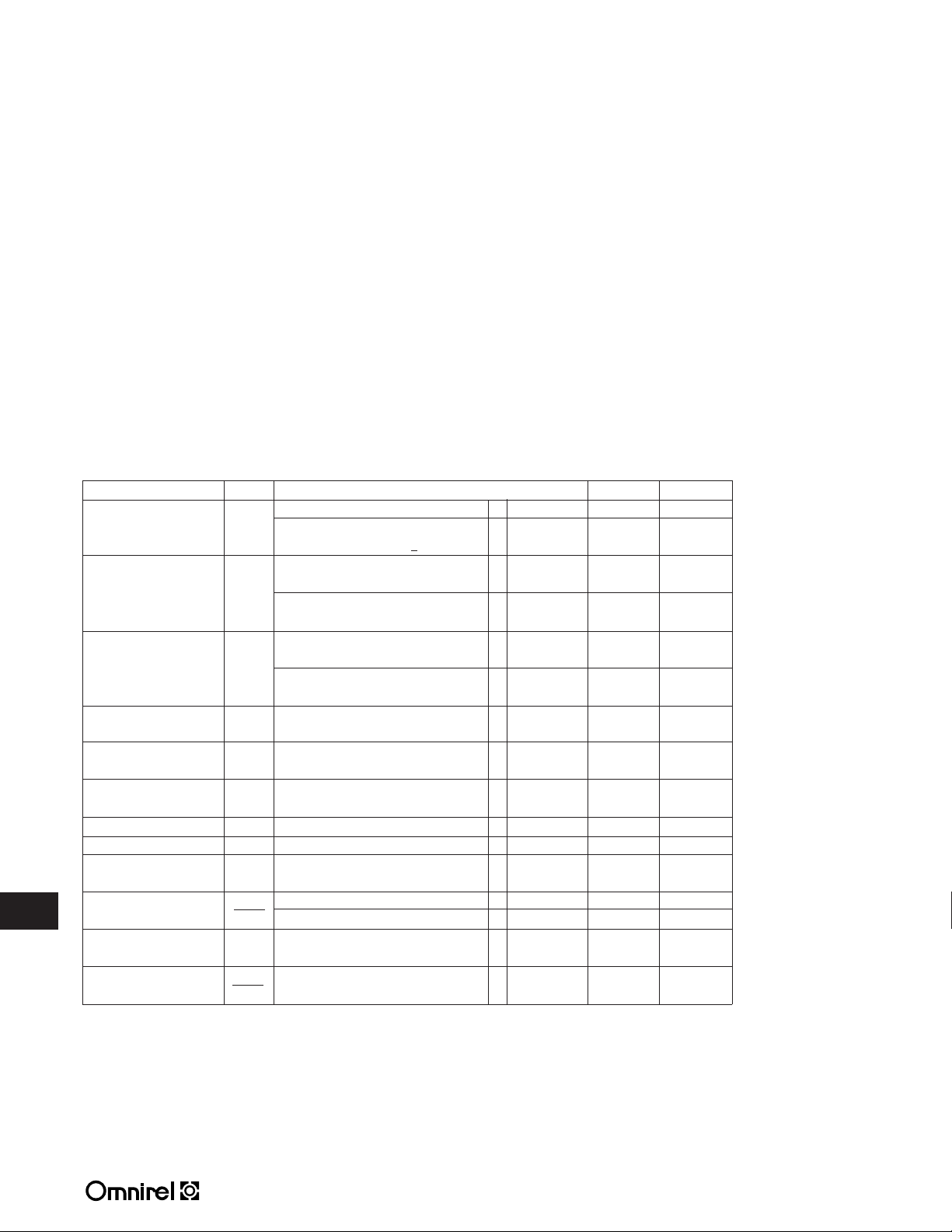
ELECTRICAL CHARACTERISTICS 5 Volt V
Parameter Symbol Test Conditions Min. Max. Unit
Output Voltage V
Line Regulation V
(Note 1)
(Note 4) V
OUT
RLINE
V
IN
I
= 5mA to 1.0 A, P < 15W
O
VIN= 7.5V to 20V 5 mV
IN
= 10V, Io= 500mA, -55°C TA 125°C (unless otherwise specified)
IN
TA= 25°C 4.92 5.08 V
= 7.5V to 20V • 4.85 5.15 V
• 12 mV
= 8.0V to 12V 4 mV
• 10 mV
Load Regulation V
(Note 1) I
RLOAD
IO = 5mA to 1.5 Amp 12 mV
= 5mA to 1.0 Amp • 25 mV
O
I
= 250mA to 750 mA 6 mV
O
• 15 mV
Standby Current Drain I
SCD
• 6.5 mA
Standby Current Drain DI
Change With Line (Line)
Standby Current Drain DI
Change With Load (Load)
Dropout Voltage V
Peak Output Current I
Short Circuit Current I
(Note 2)
Ripple Rejection DV
Output Noise Voltage N
(Note 3) RMS
Long Term Stability DV
(Note 3) Dt
DV
SCD
SCD
DO
O (pk)
DS
IN
OUT
O
OUT
V
= 7.5V to 20V • 0.8 mA
IN
IO= 5mA to 1000mA • 0.5 mA
TA= 25°C, DV
= 100mV, I
OUT
TA= 25°C 1.5 3.3 A
VIN= 35V 1.2 A
= 1.0A 2.5 V
O
• 2.8 A
f =120 Hz, DVIN= 10V 68 dB
(Note 3) • 60 dB
TA= 25°C, f =10 Hz to 100KHz 40 µV/V
TA= 25°C, t = 1000 hrs. 75 mV
6mA
Notes:
1. Load and Line Regulation are specified at a constant junction temperature. Pulse testing with low duty cycle is used.
Changes in output voltage due to heating effects must be taken into account separately.
2. Short Circuit protection is only assured up to VIN= 35V.
3. If not tested, shall be guaranteed to the specified limits.
The • denotes the specifications which apply over the full operating temperature range.
4. Minimum load current for full line regulation = 5.0 mA.
3.3 - 58
Page 3
OM1805STM/NTM - OM1815STM/NTM
.430
.410
.200
.190
.038 MAX.
.005
.120 TYP.
.537
.527
.665
.645
.420
.410
.150
.140
.750
.500
.100 TYP.
.035
.025
.045
.035
ELECTRICAL CHARACTERISTICS 12 Volt V
Parameter Symbol Test Conditions Min. Max. Unit
Output Voltage V
Line Regulation V
(Note 1)
(Note 4) V
Load Regulation V
(Note 1) I
Standby Current Drain I
Standby Current Drain DI
Change With Line (Line)
Standby Current Drain DI
Change With Load (Load)
Dropout Voltage V
Peak Output Current I
Short Circuit Current I
(Note 2)
Ripple Rejection DV
Output Noise Voltage N
(Note 3) RMS
Long Term Stability DV
(Note 3) Dt
RLINE
RLOAD
SCD
O (pk)
DV
OUT
SCD
SCD
DO
DS
OUT
OUT
IN
O
TA= 25°C, f =10 Hz to 100KHz 40 µV/V
Notes:
1. Load and Line Regulation are specified at a constant junction temperature. Pulse testing with low duty cycle is used.
Changes in output voltage due to heating effects must be taken into account separately.
2. Short Circuit protection is only assured up to VIN= 35V.
3. If not tested, shall be guaranteed to the specified limits. 4. Minimum load current for full line regulation = 5.0 mA.
The • denotes the specifications which apply over the full operating temperature range.
4. Minimum load current for full line regulation = 5.0 mA.
TA= 25°C 11.88 12.12 V
V
= 14.5V to 27V • 11.64 12.36 V
IN
I
= 5mA to 1.0 A, P < 15W
O
VIN= 14.5V to 27V 18 mV
= 16V to 22V 9 mV
IN
IO = 5mA to 1.5 Amp 32 mV
= 5mA to 1.0 Amp • 60 mV
O
I
= 250mA to 750 mA 20 mV
O
V
= 15V to 30V • 0.8 mA
IN
IO= 5mA to 1000mA • 0.5 mA
DV
= 100mV, I
OUT
TA= 25°C 1.5 3.3 A
VIN= 35V 1.2 A
f =120 Hz, DVIN= 10V 61 dB
(Note 3) • 54 dB
TA= 25°C, t = 1000 hrs. 120 mV
= 19V, Io= 500mA, -55°C TA 125°C (unless otherwise specified)
IN
• 50 mV
• 30 mV
• 40 mV
6.0 mA
• 6.5 mA
= 1.0A • 2.5 V
O
• 2.8 A
MECHANICAL OUTLINE
3.3 - 59
CONNECTION DIAGRAM
4
Case T
1 Input
2 Ground
3 Output
4 Ground
123
Case U
1 Input
2 Ground
3 Output
4 No Connection
3.3
Page 4
205 Crawford Street, Leominster, MA 01453 USA (508) 534-5776 FAX (508) 537-4246
OM1805STM/NTM - OM1815STM/NTM
ELECTRICAL CHARACTERISTICS 15 Volt V
Parameter Symbol Test Conditions Min. Max. Unit
Output Voltage V
Line Regulation V
(Note 1)
(Note 4) V
Load Regulation V
(Note 1) I
Standby Current Drain I
Standby Current Drain DI
Change With Line (Line)
Standby Current Drain DI
Change With Load (Load)
Dropout Voltage V
Peak Output Current I
Short Circuit Current I
(Note 2)
Ripple Rejection DV
Output Noise Voltage N
(Note 3) RMS
Long Term Stability DV
(Note 3) Dt
RLINE
RLOAD
SCD
O (pk)
DV
OUT
SCD
SCD
DO
DS
IN
OUT
O
OUT
= 23V, Io= 500mA, -55°C TA 125°C (unless otherwise specified)
IN
TA= 25°C 14.8 15.2 V
V
= 18.5V to 30V • 14.6 15.4 V
IN
I
= 5mA to 1.0 A, P < 15W
O
VIN= 17.5V to 30V 20 mV
• 50 mV
= 20V to 26V 15 mV
IN
• 25 mV
IO = 5mA to 1.5 Amp 35 mV
= 5mA to 1.0 Amp • 75 mV
O
I
= 250mA to 750 mA 21 mV
O
• 45 mV
6.0 mA
• 6.5 mA
V
= 18.5V to 30V • 0.8 mA
IN
IO= 5mA to 1000mA • 0.5 mA
TA= 25°C, DV
OUT
= 100mV, I
= 1.0A 2.5 V
O
TA= 25°C 1.5 3.3 A
VIN= 35V 1.2 A
• 2.8 A
f =120 Hz, DVIN= 10V 54 dB
(Note 3) • 52 dB
TA= 25°C, f =10 Hz to 100KHz 40 µV/V
TA= 25°C, t = 1000 hrs. 150 mV
3.3
Notes:
1. Load and Line Regulation are specified at a constant junction temperature. Pulse testing with low duty cycle is used.
Changes in output voltage due to heating effects must be taken into account separately.
2. Short Circuit protection is only assured up to VIN= 35V.
3. If not tested, shall be guaranteed to the specified limits.
The • denotes the specifications which apply over the full operating temperature range.
4. Minimum load current for full line regulation = 5.0 mA.
TYPICAL PERFORMANCE CHARACTERISTICS
PEAK OUTPUT
3.5
3
2.5
2
1.5
1
Output Current (A)
0.5
DV
OUT
0
0 5 10 15 20 25 30 35
Input To Output Differential (V)
Tj= 25°C
Tj= 150°C
= 100mV
Tj= -55°C
DROPOUT VOLTAGE
2.5
2
1.5
1
0.5
DV
OUT
0
-75-50 -25 0 25 50 75 100 125150
Junction Temperature (°C)
= 100MV
I
= 1A
OUT
I
= 500mA
OUT
I
= 0A
OUT
RIPPLE REJECTION
100
80
60
40
Ripple Rejection (dB)
20
0
V
- V = 8V
IN
10 100 1k 10k 100k
Frequency (Hz)
DC
I
= 1A
OUT
Tj= 25°C
+3.5V
V
OUT
rms
= 5V
 Loading...