

Page 1

Service Manual
XGA COLOR MONITOR
Model : 526X
D AEW OO ELECTR ONICS CO., LTD.
Page 2

4
◆ Electrostatically Sensitive (ES) Devices
Some semiconductor (solid state) devices can be damaged easily by static electricity.
Such components are commonly called Electrostatically Sensitive (ES) Devices.
The typical examples of ES devices are integrated circuits, some field-effect transistors, and
semiconductor “chip” components. The following techniques should be used to help reduce the incidence
of component damage caused by static electricity.
1. Immediately before handling any semiconductor component or semiconductor-equipped assembly,
wipe off any electrostatic charge on your body by touching any known earth ground. Alternatively,
obtain and wear a commercially available discharging wrist strap device which should be removed for
potential shock reasons prior to applying power to the unit under testing conditions.
2. After removing the electrical assembly equipped with ES devices, place the assembly on a conductive
surface such as aluminum foil to prevent electrostatic charge buildup or exposure to the assembly.
3. Only use a grounded-tip soldering iron to solder or unsolder ES devices.
4. Only use an anti-static type solder removal device. Some solder removal devices not classified as “antistatic” can generate enough electrical charges to damage ES devices.
5.
Do not use freon-propelled chemicals. These can generate enough electrical charges to damage ES devices.
6. Do not remove a replacement ES device from its protective package until immediately before you are
ready to install it. (Most replacement ES devices are packaged with leads electrically shorted together
by conductive foam, aluminum foil, or comparable conductive material).
7. Immediately before removing the protective material from the leads of replacement ES devices, touch
the protective material to the chassis or circuit assembly into which the device will be installed.
8. Minimize bodily movements when handling unpackaged replacement ES devices. (Otherwise harmful
motion such as the brushing together clothes fabric or the lifting your foot from a carpeted floor can
generate enough static electricity to damage ES devices).
◆ General Soldering Guidelines
1. Use a grounded-tip, low-wattage soldering iron with appropriate tip size and shape that will maintain
tip temperature between a 550°F-660°F (288°C-316°C) range.
2. Use an appropriate gauge of RMA resin-core solder composed of 60 parts tin/40 parts lead.
3. Keep the soldering iron tip clean.
4. Throughly clean the surface to be soldered. Use a small wire-bristle (0.5 inch or 1.25cm) brush with a
metal handle. Do not use freon-propelled spray-on cleaners.
5. Use the following soldering technique:
a. Allow the soldering iron tip to reach normal temperature (550°F to 660°F or 288°C to 316°C)
b. Hold the soldering iron tip and solder strand against the component lead until the solder melts.
c. Quickly move the soldering iron tip to the junction of the component lead and the printed circuit foil,
and hold it there until the solder flows onto and around both the component lead and the foil.
d.
Closely inspect the solder area and remove any excess or splashed solder with a small wire-bristle brush.
CAUTION:
Be sure that no power is applied to the chassis or circuit, and observe all other safety
precautions.
CAUTION: Work quickly to avoid overheating the circuit board printed foil.
Page 3

5
FIGURE 1. USE SOLDERING IRON TO PRY LEADS
◆ IC Removal/Replacement
Some utilized chassis circuit boards have slotted (oblong) holes through which the IC leads are inserted
and then bent flat against the circuit foil. When holes are slotted, the following technique should be used
to remove and replace the IC. When working with boards using the familiar round hole, use the standard
technique as outlined in paragraphs 5 on the page under the title of general soldering guidelines.
◆ Removal
1. Desolder and straighten each IC lead in one operation by gently prying up on the lead with the
soldering iron tip as the solder melts.
2. Draw away the melted solder with an anti-static suction-type solder removal device (or with
desoldering braid before removing the IC.
◆ Replacement
1. Carefully insert the replacement IC in the circuit board.
2. Carefully bend each IC lead against the circuit foil pad and solder it.
3. Clean the soldered areas with a small wire-bristle brush. (lt is not necessary to reapply acrylic coating
to the area).
◆ “Small-Signal” Discrete Transistor Removal/Replacement
1. Remove the defective transistor by clipping its leads as close as possible to the component body.
2. Bend the ends of each of three leads remaining on the circuit board into a “U” shape.
3. Bend the replacement transistor leads into a “U” shape.
4. Connect the replacement transistor leads to the corresponding leads extending from the circuit board
and crimp the “U” with long nose pliers to ensure metal-to-metal contact, then solder each connection.
Page 4

6
◆ Power IC, Transistor or Devices Removal/Replacement
1. Heat and remove all solders from the device leads.
2. Remove the heatsink mounting screw (if applicable).
3. Carefully remove the device from the circuit board.
4. Insert new device in circuit board.
5. Solder each device lead and then clip off excess lead.
6. Replace heatsink.
◆ Diode Removal/Replacement
1. Remove defective diode by clipping its leads as close as possible to diode body.
2. Bend the two remaining leads perpendicularly to the circuit board.
3. Observing diode polarity, wrap each lead out of the new diode around the corresponding lead on the
circuit board.
4. Securely crimp each connection and solder it.
5. Inspect the solder joints of the two “original” leads on the circuit board copper side. If they are not
shiny, reheat them and apply additional solder if necessary.
TECHNICAL INFORMATION
CDT Size 15-inch
Diagonal visible image area 14-inch
Dot Pitch 0.28 mm
Synchronization Horizontal 30 - 54 KHz
Vertical 50 - 160 Hz
Plug and Play DDC1/2B/CI
Power Saving EPA, VESA DPMS, Nutek Compliant
Power Source 100-240 Vac, 50/60Hz (Free Voltage)
Power Consumption 70W
Dimension-W x H x D 360 x 381 x 389mm
(set with stand)
Weight-unpacked(lbs/Kg) 25.1/11.4
Operating Temperature 10 ~ 40°C /50 ~ 104°F
Page 5

This color monitor automatically scans all horizontal frequencies from 30KHz to 54KHz, and all vertical frequencies from
50Hz to 160Hz. This color monitor supports IBM PC, PC/XT, PC/AT, personal System/2 (PS/2), Apple Macintosh, and
compatible users crisp text and vivid color graphics display when using the following graphics adapters : (VGA, 8514/A,
Super VGA, VESA and XGA and Apple Macintosh Video Card). And so, this color monitor has a maximum horizontal
resolution of 1024 dots and a maximum vertical resolution of 768 lines for superior clarity of display.
By accepting analog signal inputs which level is zero to 0.7 Volts. This color monitor can display and unlimited palette of
colors depending on the graphics adapter and software being used.
◆ Abbreviations
7
GENERAL INFORMATION
ADJ Adjustment
AFC Automatic Frequency Control
CRT Cathode Ray Tube
Def Deflection
D.Y Deflection Yoke
FBT Flyback Transformer
H.SYNC Horizontal Synchronization
OSC Oscillator
P.S.U Power Supply Unit
PWA Printed Circuit Board Wiring Assembly
R.G.B Red, Green, Blue
V.Sync Vertical Synchronization
Page 6

8
Pin Signal
1 Red
2 Green
3 Blue
4 GND
5 GND
6 GND - Red
7 GND - Green
8 GND - Blue
9 +5Vdc
10 GND - H.Sync
11 GND - V.Sync
12 Bi-directional Data (SDA)
13 Horizontal Sync
14 Vertical Sync (VCLK)
15 Data Clock (SCL)
• Degaussing is always required when adjusting purity or convergence.
• The white balance adjustment has been done by a color analyzer in factroy. The adjustment procedure,
described in the service manual is made by a visual check.
• Allow 20 minutes warm-up time for the display before checking or adjusting only electrical
specification or function.
• Reform the leadwire after any repair work.
◆ Caution For Servicing
• In case of servicing or replacing CRT, high voltage sometimes remains in the anode of the CRT. Completely
discharge high voltage before servicing or replacing CRT to prevent a shock to the serviceman.
Arrangement of 15-pin D-sub connector
PIN CONNECTOR
CAUTIONS FOR ADJUSTMENT AND REPAIR
1
6
15
10
Page 7

9
OPERATION AND ADJUSTMENT
Control Panel
• Launch OSD(On-Screen Display) MENU window.
• Select a sub Menu & function.
• Move a sub Menu & function.
• Increase the value of any selected function.
• Adjust the contrast directly when there is no OSD.
• Move a sub Menu & function.
• Decrease the value of any selected function.
• Adjust the brightness directly when there is no OSD.
MENU
SELECT
ADJUST
MENU
SELECT
Page 8
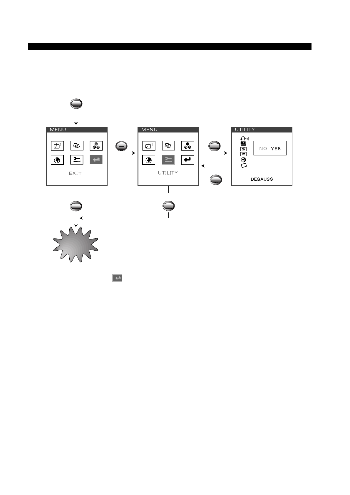
10
Key Process
•
When you choose the icon on the OSD window, you can exit the OSD screen.
MENU
SELECT
OSD OFF
MENU
MENUMENU
Page 9

11
OSD Functions
ICON CONTROL FUNCTIONS
Adjust the pin corner bottom when the bottom sides of the screen are bowed.
B. PIN CORNER
Adjust the side pin corner balance top when the top sides of the screen are bowed
towards left or right.
T. PIN BALANCE
Adjust the side pin corner balance bottom when the bottom sides of the screen are bowed
towards left or right.
B. PIN BALANCE
Adjust the parallelogram when the screen is leaning left or right.
Adjust the pin corner top when the top sides of the screen are bowed.
T. PIN CORNER
PARALLELOGRAM
Adjust the trapezoid of the screen by moving the lines inward or outward.
Adjust the side balance when the sides of the screen are bowed towards left or right.
PIN BALANCE
TRAPEZOID
Adjust the left and right margins for more convex or more concave margins.
PINCUSHION
Adjust the display height (vertical size).
Adjust the vertical linearity.
V. LINEARITY
V.SIZE
Adjust the position of the display vertically (up or down).
Adjust the display width (horizontal size).
H.SIZE
V. POSITION
Adjust the position of the display horizontally (left or right). H. POSITION
Choose different preset color temperatures or set your own customized color parameters.
COLOR TEMP
Page 10

12
Reset the screen to the Factory Preset Display Settings.
RECALL
ICON CONTROL FUNCTIONS
Display horizontal & vertical frequency and polarity.
STATUS
Adjust the rotation when the screen is tilted left or right (Optional).
ROTATION
Adjust the vertical picture moire cancellation.
V. MOIRE
Adjust the horizontal picture moire cancellation.
H. MOIRE
Degaussing keeps the monitor free from unwanted magnetism that can result in color
impurity.
DEGAUSS
Adjust the blue bias.
BLUE BIAS
Select language for OSD (5 languages).
LANGUAGE
Adjust the green bias.
GREEN BIAS
Adjust the red bias.
RED BIAS
Adjust the red gain.
Adjust the green gain.
Adjust the blue gain.
RED GAIN
GREEN GAIN
BLUE GAIN
Page 11

ALIGNMENT PROCEDURE
◆ Standard Adjustment Conditions
1. Power source voltage : 100-240Vac 50/60Hz
2. Aging : Take at least 20 minutes warm-up time.
3. Signals
Video : Analog 0.7Vpp 75Ω terminal positive polarity
Synchronizing : TTL level Negative/Positive Separate
Deflection frequency
Horizontal Frequency : 30KHz - 54KHz
Vertical Frequency : 50Hz - 160Hz
◆ Pre-Adjustment
1. B+ Adjustment
Adjust 6.15Vdc ± 0.05Vdc between P503 and ground at 31.5KHz mode, varying VR001.
Adjust -150Vdc ± 0.5Vdc between P504 and ground at 31.5KHz mode, varying VR501.
◆ Method to launch the factory mode
Step 1. Push the menu button.
Step 2. Push the menu button and plus control button ( + ) for 5 times in same time.
◆ Main Adjustment
1. Setting the Controls
Set the value of items as following.
Contrast : Max.(OSD value up to MAX)
Brightness : Center(Set the OSD value to center)
2. H.size, V.size, H.phase, V.position, Pincushion, Trapezoid
Receive the cross hatch pattern of Factory preset mode.
H.size, V.size, H.phase, V.position, Pincushion, Trapezoid are adjusted at each mode.
In Factory, Auto Alignment was done at each mode. Therefore, Factory preset mode has it’s
own value according to each control.
3. Focus
(a) Set brightness control to center and contrast control to MAX.
(b) Receive all “H” character pattern of 1024 X 768 (48KHz, 60Hz)
(c) Adjust the Focus control of FBT to obtain best Focus.
4. Geometric Distortion Adjustment.
(a) Receive the cross hatch pattern of factory preset mode.
(b) Pincushion, Trapezoid are adjusted the best geometric status.
5. White Balance Adjustment
(a) Select 9300°K on the OSD Menu.
(b) Receive a full white pattern of 54KHz mode signal by using the signal generator.
(c) Set the brightness control to the maximum, the contrast control to the maximum.
(d) Cut off the FBT screen VR.
(e) Receive all the black patterns. The luminance of the screen should be 0.5~1.0 Ft-L by using Screen
VR.
(f) Select the R-BIAS, G-BIAS and B-BIAS on the control menu and adjust the +/– key to get the color
coordinates in x=0.281 ± 0.015, y=0.311± 0.015.
(g) Receive a full white pattern. Adjust the brightness value to the center.
(h) Select the R-GAIN and B-GAIN and adjust the +/– key to get the color coordinates in x=0.281 ±
0.015, y=0.311 ± 0.015.
(i) Adjust the ABL control to get the screen luminance to 30 Ft/L (a full white pattern over 30 Ft/L)
(j) Check if the x, y coordinates of color analyzer is in x=0.281±0.015, y=0.311±0.015.
If the color coordinates is out of range, adjust the R. G. B BIAS & GAIN to get the coorinates in
x=0.281, y=0.311. Make sure that the coordinates is in range.
(k) Select 6550°K on the OSD Menu and set the color coordinates in x=0.313, y=0.329 at the
maximum contrast control and center brightness control
(l) Check if a full white pattern is over 30Ft/L.
13
Page 12

14
6. Static Convergence Adjustment
(a) Apply a magenta cross hatch pattern on display.
(b) Adjust the focus from the best over all focus on the display.
Also adjust the brightness to the desired condition.
(c) Vertical red and blue lines are converged by varying the angle between the two tabs of the 4-pole
magnets.
(d) Horizontal red and blue lines are converged by varying the tabs together, keeping the angle between
them constant.
(e) Apply a yellow cross hatch pattern on display.
(f) Vertical green and red lines are converged by barying the angle between the two tabs of the 6-pole
magnets.
(g) Horizontal green and red lines are converged by varying the tabs together, keeping the angle
between them constant.
Page 13

15
TROUBLESHOOTING HINTS
1. No Character
Are the Contrast &
Brightness Controls in
OSD menu
maximum?
Change the Contrast &
Brightness control value to
maximum
No Raster
Refer to
No Raster
Check the peripheral circuit
of CRT
Check the video output
circuit and its ambient circuit
Trouble in 12V line
of the Main PWB
Check the clamping pulse
circuit
Check the signal cable
No Character
Is whole
screen bright?
Yes
Yes
Yes
Yes
Yes
No
No
No
No
No
Yes
Yes
Rk, Gk, Bk
About 30~35Vpp
No
No
Is CRT
Cathode (Rk, Gk, Bk)
signal level
normal?
Is the
output signal of the
(pin 21,24,26) pre-amp
IC801, normal?
Is clamping
pulse (pin 18 of IC801)
normal?
Is 12V line
normal?
Is input signal
normal?
Trouble in IC801 and
its ambient circuit
5Vp-p
Page 14

16
2. No Raster
Trouble in
power supply
circuit
Trouble in power
supply circuit
Trouble in G1
line
Trouble in FBT or its
pin 4 ambient circuit
High Voltage
trouble in FBT
Trouble in 100Vdc
line of power
supply unit
Refer to trouble
in P.S.U
Refer to trouble in
power supply unit.
Is CRT
heater red-hot?
No
No
No
No
No
No
No
Yes
Yes
Yes
Yes
Yes
Yes
Yes
Yes
Is Heater
Voltage (CRT PWB)
about 6V?
Turn the Brightness
& Contrast control
to set Maximum
No Raster
Is whole
screen bright?
Check
G1 voltage about
-40V?
Is 100Vdc
line normal?
Does
the Brightness
control make screen
bright?
Is CRT
G2 (screen) voltage
about 500V?
Trouble in
CRT
Trouble in FBT
Page 15

17
3. A Missing Color
Is input signal
normal?
One color is
missing
CRT
Cathode (Rk, Gk, Bk)
is normal?
Is video
output IC802 waveform
normal?
Each grid (G1, G2)
voltage normal?
Is the
output of pre-amp
(IC801, KA2500)
pin 21, 24, 26 all
normal?
Check video signal
cable or video card.
Trouble in IC801 or its
ambient circuit
Trouble in
video output
circuit, IC802
or ambient
Trouble in 100Vdc line
Trouble in G1,G2 line
Replace CRT
No
No
No No
No
Yes
Yes Yes
Yes
Yes
RK, GK, BK
About 40V p-p
0.7Vpp
Page 16

18
4. Abnormal OSD Font
Is menu
key selected?
Is OSD Font
exist?
* If menu key selected.
Is Heater
Voltage about 6V?
Abnormal OSD Font
Is the
output of IC803
(pin 12,13, 14)
normal?
Trouble in
Heater voltage
line.
Refer to trouble in P.S.U
Troubie in
IC803 or its
ambient circuit
Trouble in IC803
and its ambient
circuit
One color is
missing
Refer to Missing Color
No
No
Yes
Yes
Yes
Yes
No
Page 17

MODE B+ Voltage
VGA 72Vdc
Super VGA
86Vdc
54KHz 124Vdc
19
5. Horizontal Output Circuit
Is the
B+line voltage
over 175V?
Is the H-out
waveform of IC501
normal?
Trouble in IC501
Trouble in Horizontal
output circuit
(No Raster)
Yes
No
Is the Gate wave
form of
Q553 normal?
Yes
Yes
Yes
Trouble in Q553
Trouble in Q551, Q552
No
No
No
Trouble in Q554 and
its ambient circuit.
10V
0V
11V
0V
66V
Is the Drain
waveform of
Q553 normal?
Trouble in 175V line.
Page 18

20
6. Unstable Picture
6-1. Horizontal
Unstable
picture
Is H.Sync
input pin of IC501
correct?
Check H.Sync Out of
Micom or its ambient
circuits.
Yes
No
Trouble in IC501
Page 19

21
6-2. Vertical
Unstable
picture
Is the
12V,-12Vdc
line voltage is
correct?
Refer to P. S. U
Is the
pulse of pin 5 of
the IC401
correct?
Trouble in
vertical D. Y
No
No
No
Yes
Yes
Is the output
of pin 4 of IC501
all normal?
Check IC401 and
its ambient circuit
Yes
Check the IC501 and
its ambient circuit
50Vp-p
40V
-10V
Page 20

22
7. Focus
Monitor remains
unfocused
Check
Focus VR in
FBT
Is
focus
acceptable?
Trouble in Focus
circuit (FBT)
Yes
OK
No
Page 21

23
8. Convergence
Is
convergence
on the center area
bad?
Is
convergence on the
fringe area bad?
Adjust static
convergence
Refer to
Adjustment
procedure of
convergence
Yes
Adjust D.Y
Location
Yes
No
Poor convergence
Page 22

MODE B+ Voltage
VGA 72Vdc
Super VGA
86Vdc
54KHz 124Vdc
24
9. Abnormal Picture
9-1. Horizontal Size
Trouble in L835,
C543 or their ambient
circuit
Trouble in Horizontal
output circuit
Check the B+ and
anode voltage of CRT.
Trouble in H.OSC/
Deflection Circuit
Refer to Horizontal Output circuit
Is
the DC level
of the base of Q509
changeable?
No
Yes
Is
the DC level
of IC501 pin 5
changeable ?
Yes
Check IC501
pin 5
Is the
collector pulse
of Q554 correct?
Is the
cathode waveform
of D568
correct?
Abnormal
H.Size
=1100Vp-p
80-310Vpp
*
Normally anode voltage
of CRT is approximately,
24KV
*
Scan B+ are as follow :
No
Yes
Yes
No
*
At first, adjust controls in the OSD Menu
Page 23

25
9-2. Vertical Size
Is
changeable the
DC voltage of
IC401 pin 1?
Check the IC4
and its
ambient circuit
Check the IC501 and
its ambient circuit
No
No
Trouble V.OSC/
Deflection Circuit
Refer to V.OSC/Deflection circuit
Yes
Is
the 3.5Vdc of pin
4 of the IC501?
Yes
Abnormal
V.Size
Page 24

26
10. Side-Pincushion Circuit
Side-Pincusion distortion
is excessive or barrel
O.K
Select the
side-pincushion
icon on OSD menu,
and adjust acceptable
position.
Yes
Check IC501 or
their ambient circuit
(pin 13, 14)
Is the pin 5
waveform of IC501
correct
Yes
No
Trouble in IC501
No
Page 25

27
11. Power Supply Unit (P.S.U)
Is the
IC001
O.K?
Replace IC001
No
Is
voltage of C104
50Vdc?
No
Is
voltage of D002
130V (270V)?
Trouble in switching
power transformer T001
or IC001 and its ambient
circuit
Trouble in diode
D001,D002,D003,D004
or peripheral device
No
Is the
waveform of T001
pin5 correct?
Trouble in T001
or D101
No
Trouble in P.S.U
Is
power switch
on?
Switch on
No
Yes
Yes
Yes
Yes
Yes
Yes
Is
voltage of C101
100Vdc?
Trouble in T001 or D102
No
Is
fuse F001
O.K?
Check the power cord outlet
and diode D001,D002,D003,D004
No
A
Page 26

28
Is voltage
of C112
25Vdc?
Trouble in D105
No
Is voltage
of C117 14.3Vdc?
No
Yes
Yes
Yes
Is
voltage of C643
-15Vdc?
Trouble in D643 or vertical
Part.
P.S.U O.K
Trouble in D103 or
horizontal Part.
No
A
Page 27

R,G,B
SCL SDA
EPROM
( 24LC08)
MCU
(KS88C6224)
H.OSC
&
V.DRV
(1888CT)
SCL
H.SYNC
V.SYNC
SDA
DEGAUSSING
CIRCUIT
DEGAUSS CONTROL
DPMS CONT.
OUTPUT
REGULATOR
MAIN
POWER
SYNC
TRANS
(DST-603)
H.DRV
SYNC.
TRIGGERING
SMPS
TRANSFORMER
SMPS
CONTROL
(KA3842)
+12V,+5V
VIDEO
POWER
FBT
H.DY
V.DRV
AMP
(TDA8172)
H.DRV
B+
CONTROL
(uPC1555C)
V. DY
H.SIZE
& G/D
C0NTROL.
H. LIN
COIL
H.CS
BLOCK
H.
IZE FB
AN B+
X-RAY
PROTECT
H/V
CONTROL
(KA7500)
HV.DRV
BUCK
TRANS
LED
H
FBP
G1
CONTROL
G1
MUTE
CLAMP&BLANKING
PULSE
HIGH VOLTAGE
SCREEN &
FOCUS
15PIN
D-SUB
RECEPTACLE
(02WE4E1)
VIDEO
PREAMP
(KA2500)
VIDEO
OUTPUT
AMP
(TDA9532)
OSD IC
(KS2508)
TACT S/W BUTTON
(4 BUTTON)
POWER
TACT
S/W
CRT
BRIGHT CONTROL
R,G,B BIAS
MAIN BLOCK DIAGRAM VIDEO BLOCK DIAGRAM
80V
12V, 5V
100V, 12V
50V, -12V
5V, 6.3V
B+
BUCK L.
H.
YN
V.
YN
F
B
ABL
ADJUST
ROTATION
(OPTION)
Page 28

Page 29

Page 30

34
RESISTOR Description
Example:
CAPACITOR Description
Example:
Fig &
Part No Description
Index
Capacitors
C102 CCXF1H104Z Ceramic 50V 0.1µF Z
C402 CCXB1H331K Ceramic 50V 330PF K
C105 CMXM 2A224J MYLAR 100V 0.22µF J
Allowance
C ± 0.25pF
D ± 0.5%
F ± 1pF
J±5%
K ± 10%
P ± 100% ~ 0%
Z ± 80% ~ –
Fig &
Part No Description
Index
R101
Resistors
RD-4Z820J Carbon: 82J
R102 RD-4Z201J Carbon1/4W-200J
Allowance
F±1%
J±5%
K ± 10%
M ± 20%
G±2%
INFORMATION OF PART DESCRIPTION
Important Safety Notice
Components identified with the International Symbol have special characteristics important for safety.
When replacing any components, use only manufacturer’s specified parts.
Abbreviation of Description
Page 31

C206 CEXF1H479V C ELECTRO 50V RSS 4.7MF (5X11) TP
C207 CCZF1H104Z C CERA 50V HIKF 0.1MF Z
C208 CCZB1H102K C CERA 50V B 1000PF K
C209 CCZF1H104Z C CERA 50V HIKF 0.1MF Z
C210 CCZB1H681K C CERA 50V B 680PF K
C211 CCZB1H681K C CERA 50V B 680PF K
C212 CCZB1H681K C CERA 50V B 680PF K
C213 CCZB1H681K C CERA 50V B 680PF K
C214 CCZF1H104Z C CERA 50V HIKF 0.1MF Z
C215 CCZF1H104Z C CERA 50V HIKF 0.1MF Z
C231 CCZB1H181K C CERA 50V B 180PF K AXIAL
C232 CCZB1H181K C CERA 50V B 180PF K AXIAL
C301 CCXB2H102K C CERA 500V B 1000PF K (TAPPING)
(C1)
C401 CCXB1H271K C CERA 50V B 270PF K (TAPPING)
C402 CMXM2A562J C MYLAR 100V 5600PF J (TP)
C404 CMXL2E104J C MYLAR MEU 250V 0.1MF J
C405 CMXM2A273J C MYLAR 100V 0.027MF J (TP)
C406 CMXL2A224J C MYLAR 100V MEU 0.22MF J
C407 CEXF1C102V C ELECTRO 16V RSS 1000MF (10X20) TP
C408 CCZF1H104Z C CERA 50V HIKF 0.1MF Z
C409 CMXL2A224J C MYLAR 100V MEU 0.22MF J
C410 CEXF1V101V C ELECTRO 35V RSS 100MF (8X11.5) TP
C411 CCZF1H104Z C CERA 50V HIKF 0.1MF Z
C501 CMXM2A333J C MYLAR 100V 0.033MF J (TP)
C502 CEXF1H330V C ELECTRO 50V RSS 33MF (6.3X11) TP
C503 CCZF1H104Z C CERA 50V HIKF 0.1MF Z
C504 CMXL1J105J C MYLAR MEU 63V 1MF J
C505 CEXF1H100V C ELECTRO 50V RSS 10MF (5X11) TP
C506 CCZB1H102K C CERA 50V B 1000PF K
C507 CMXM2A222J C MYLAR 100V 2200PF J (TP)
C508 CCZF1H104Z C CERA 50V HIKF 0.1MF Z
C509 CEXF1C331V C ELECTRO 16V RSS 330MF (8X11.5) TP
C510 CEXF1H109V C ELECTRO 50V RSS 1MF (5X11) TP
C511 CEXF1H100V C ELECTRO 50V RSS 10MF (5X11) TP
C512 CCZB1H102K C CERA 50V B 1000PF K
C513 CXSL1H391J C CERA 50V SL 390PF J
C514 CCXB1H102K C CERA 50V B 1000PF K (TAPPING)
C515 CEXF1H109V C ELECTRO 50V RSS 1MF (5X11) TP
C516 CCZB1H101K C CERA 50V B 100PF K
C517 CEXF1H100V C ELECTRO 50V RSS 10MF (5X11) TP
C518 CCZB1H181K C CERA 50V B 180PF K AXIAL
C519 CCZB1H181K C CERA 50V B 180PF K AXIAL
C520 CCZF1H103Z C CERA 50V F 0.01MF Z
C521 CEXF1C331V C ELECTRO 16V RSS 330MF (8X11.5) TP
C522 CEXF1C470V C ELECTRO 16V RSS 47MF (5X11) TP
C531 CCXB3A101K C CERA 1KV B 100PF K
00001 9979800516 PCB MAIN T=1.6*246*310
00020 WNA75N031- CORD POWER SP502B+IS14 3ASL/100
B001 5PB14865-- COIL BEAD BI-4865(5TS)
B003 5PB13890-- COIL BEAD BI3890
B004 5PB13890-- COIL BEAD BI3890
(J004)
B005 5PB13890-- COIL BEAD BI3890
(J003)
B101 5PB13857-- COIL BEAD BI3857(AXIAL)
B102 5MBFD3512R COIL BEAD BFD 3512 R2
B301 5PB13857-- COIL BEAD BI3857(AXIAL)
(B1)
B501 5PB13857-- COIL BEAD BI3857(AXIAL)
B502 5PB13857-- COIL BEAD BI3857(AXIAL)
B809 5PB13857-- COIL BEAD BI3857(AXIAL)
B810 5PB13857-- COIL BEAD BI3857(AXIAL)
C001 CL1UC3104M C LINE ACROSS WORLD AC250V 0.1UF M R.47
C004 CH1FDF222M C CERA AC 2.5KV 2200PF M AC250V
C005 CEYP2G221Z C ELECTRO 400V SMH 220MF (25.4*40)
C006 CCXE3D103P C CERA HIKE 2KV 0.01MF P
C007 CEXF1E101V C ELECTRO 25V RSS 100MF (6.3X11) TP
C008 CCZF1H104Z C CERA 50V HIKF 0.1MF Z
C009 CMXL2A334J C MYLAR MEU 100V 0.33MF J
C010 CMXM2A332J C MYLAR 100V 3300PF J (TP)
C011 CMXM2A104J C MYLAR 100V 0.1MF J (TP)
C012 CCXB1H152K C CERA 50V B 1500PF K (TAPPING)
C013 CCXB3A271K C CERA 1KV B 270PF K (TAPPING)
C014 CMXM2A222J C MYLAR 100V 2200PF J (TP)
C015 CCZB1H102K C CERA 50V B 1000PF K
C101 CEXF2C470V C ELECTRO 160V RSS 47MF (13X25) TP
C102 CCXF2H103Z C CERA HIKF 500V 0.01MF Z
C103 CCXB3A471K C CERA 1KV B 470PF K (T)
C104 CEXF1J221V C ELECTRO 63V RSS 220MF (10X20) TP
C105 CCXB3A221K C CERA 1KV B 220PF K (TAPPING)
C106 CEXF1E471V C ELECTRO 25V RSS 470MF (10X16) TP
C107 CEXF1C101V C ELECTRO 16V RSS 100MF (6.3X11) TP
C108 CEXF1C102V C ELECTRO 16V RSS 1000MF (10X20) TP
C109 CEXF1C102V C ELECTRO 16V RSS 1000MF (10X20) TP
C110 CEXF1C471V C ELECTRO 16V RSS 470MF (10X12.5)TP
C111 CEXF1J221V C ELECTRO 63V RSS 220MF (10X20) TP
C302 CCXE3D103P C CERA HIKE 2KV 0.01MF P
(C2)
C201 CCZB1H181K C CERA 50V B 180PF K AXIAL
C202 CEXF1C101V C ELECTRO 16V RSS 100MF (6.3X11) TP
C203 CXCH1H220J C CERA 50V CH 22PF J (TAPPING)
C204 CXCH1H220J C CERA 50V CH 22PF J (TAPPING)
C205 CEXF1H108V C ELECTRO 50V RSS 0.1MF (5X11) TP
35
LOC PART-CODE PART-NAME PART-DESC LOC PART-CODE PART-NAME PART-DESC
ELECTRICAL P ARTS LIST
The components identified by mark ! have special characteristics important for safety and x-ray radiation.
These should be replaced only with the types specified in the parts list.
!
!
!
!
!
!
Page 32

C828 CCZB1H391K C CERA 50V B 390PF K
C829 CCXF1H103Z C CERA 50V F 0.01MF Z (TAPPING)
C830 CEXF1C101V C ELECTRO 16V RSS 100MF (6.3X11) TP
C831 CCXF2H103Z C CERA HIKF 500V 0.01MF Z
CA8019970780032 CONN AS SMH250+51088+20379#28=250
CDT 9979615003 CDT M36KXU110XX61(T)
CGND 9970710243 CRT GND AS 0.12*6*16+BL101NG*2=580
CT301 9979300013 SOCKET CRT PCS629-03A
CW301 9979220009 CONN WAFER SMW250-08
CW801 485923272S CONN WAFER 5267-06A STICK TYPE
CW802 485923282S CONN WAFER 5267-07A STICK TYPE
D001 D2A05----- DIODE 2A05
D002 D2A05----- DIODE 2A05
D003 D2A05----- DIODE 2A05
D004 D2A05----- DIODE 2A05
D005 DD2L20U--- DIODE D2L20U
D006 DHER107--- DIODE HER107
D007 DZN4148--- DIODE 1N4148 AUTO 52MM
D008 DZN4148--- DIODE 1N4148 AUTO 52MM
D101 DRU1P----- DIODE RU 1P (TAPPING)
D102 DRG4------ DIODE RG4
D103 DD2L20U--- DIODE D2L20U
D104 DD2L20U--- DIODE D2L20U
D105 DZN4148--- DIODE 1N4148 AUTO 52MM
D106 DD2L20U--- DIODE D2L20U
D201 DZN4148--- DIODE 1N4148 AUTO 52MM
D202 DZN4148--- DIODE 1N4148 AUTO 52MM
D203 DZN4148--- DIODE 1N4148 AUTO 52MM
D204 DZN4148--- DIODE 1N4148 AUTO 52MM
D231 DZN4148--- DIODE 1N4148 AUTO 52MM
D232 DZN4148--- DIODE 1N4148 AUTO 52MM
D402 D1N4002A-- DIODE 1N4002
D501 DZN4148--- DIODE 1N4148 AUTO 52MM
D502 D1NS4----- DIODE 1NS4
D503 DZN4148--- DIODE 1N4148 AUTO 52MM
D531 D1A5G----- DIODE 1A5G
D554 DDTV32F--- DIODE DTV32F
D556 D1N4937GP- DIODE 1N4937GP (TAPPING)
D561 D1A5G----- DIODE 1A5G
D567 DZN4148--- DIODE 1N4148 AUTO 52MM
D568 DRG4------ DIODE RG4
D569 DER206---- DIODE ER206
D570 DER206---- DIODE ER206
D590 D1A5G----- DIODE 1A5G
D802 DZN4148--- DIODE 1N4148 AUTO 52MM
D804 DZN4148--- DIODE 1N4148 AUTO 52MM
D806 DZN4148--- DIODE 1N4148 AUTO 52MM
D831 DZN4148--- DIODE 1N4148 AUTO 52MM
D832 DZN4148--- DIODE 1N4148 AUTO 52MM
D833 DZN4148--- DIODE 1N4148 AUTO 52MM
D845 DZN4148--- DIODE 1N4148 AUTO 52MM
C535 CMXA2G474J C MYLAR MPA 400V 0.47MF J
C536 CMXM2A223J C MYLAR 100V 0.022MF J TP
C537 CMYF2D624J C MYLAR 200V MPP 0.62MF J
C538 CMXF2D224J C MYLAR MPP 200V 0.22MF J
C540 CEXF1H109V C ELECTRO 50V RSS 1MF (5X11) TP
C541 CEXF1C101V C ELECTRO 16V RSS 100MF (6.3X11) TP
C542 CMXM2A332J C MYLAR 100V 3300PF J (TP)
C543 CMXL1J105J C MYLAR MEU 63V 1MF J
C545 CEXF1H100V C ELECTRO 50V RSS 10MF (5X11) TP
C546 CEXF1H478V C ELECTRO 50V RSS 0.47MF (5X11) TP
C547 CEXF2E100V C ELECTRO 250V RSS 10MF (10X20) TP
C548 CMXM2A223J C MYLAR 100V 0.022MF J TP
C550 CMXM2A104J C MYLAR 100V 0.1MF J (TP)
C551 CEXF2A100V C ELECTRO 100V RSS 10MF (6.3X11) TP
C552 CMXM2A104J C MYLAR 100V 0.1MF J (TP)
C553 CCXB2H102K C CERA 500V B 1000PF K (TAPPING)
C554 CEXF1H220V C ELECTRO 50V RSS 22MF (5X11) TP
C555 CMXM2A393J C MYLAR 100V 0.039MF J (TP)
C556 CMXE2J103J C MYLAR 630V PL 0.01MF J
C557 CMYH3C682J C MYLAR BUP 1.6KV 6800PF J BULK
C558 CMXM2A223J C MYLAR 100V 0.022MF J TP
C559 CMYF2D225J C MYLAR MPP 200V 2.2MF J
C560 CEXF1H100V C ELECTRO 50V RSS 10MF (5X11) TP
C561 CEXF1H479V C ELECTRO 50V RSS 4.7MF (5X11) TP
C577 CCXB2H331K C CERA 500V B 330PF K (TAPPING)
C801 CCZF1H104Z C CERA 50V HIKF 0.1MF Z
C802 CCZB1H102K C CERA 50V B 1000PF K
C803 CEXF1C470V C ELECTRO 16V RSS 47MF (5X11) TP
C804 CMXM2A104J C MYLAR 100V 0.1MF J (TP)
C806 CEXF1H109V C ELECTRO 50V RSS 1MF (5X11) TP
C807 CCZB1H223K C CERA HIBK 50V 0.022MF K AXL 52
C808 CCZF1H104Z C CERA 50V HIKF 0.1MF Z
C809 CEXF1C470V C ELECTRO 16V RSS 47MF (5X11) TP
C810 CEXF1H100V C ELECTRO 50V RSS 10MF (5X11) TP
C811 CCZF1H104Z C CERA 50V HIKF 0.1MF Z
C812 CEXF1H100V C ELECTRO 50V RSS 10MF (5X11) TP
C813 CCZF1H104Z C CERA 50V HIKF 0.1MF Z
C814 CEXF1H100V C ELECTRO 50V RSS 10MF (5X11) TP
C815 CCZF1H104Z C CERA 50V HIKF 0.1MF Z
C816 CEXF1C470V C ELECTRO 16V RSS 47MF (5X11) TP
C817 CCZF1H104Z C CERA 50V HIKF 0.1MF Z
C818 CCZF1H104Z C CERA 50V HIKF 0.1MF Z
C819 CCZF1H104Z C CERA 50V HIKF 0.1MF Z
C820 CCZF1H104Z C CERA 50V HIKF 0.1MF Z
C821 CCZF1H104Z C CERA 50V HIKF 0.1MF Z
C822 CCZF1H104Z C CERA 50V HIKF 0.1MF Z
C823 CCZF1H104Z C CERA 50V HIKF 0.1MF Z
C824 CMXM2A153J C MYLAR 100V 0.015MF J (TP)
C825 CEXF1C470V C ELECTRO 16V RSS 47MF (5X11) TP
C826 CCZF1H104Z C CERA 50V HIKF 0.1MF Z
C827 CCZB1H391K C CERA 50V B 390PF K
36
LOC PART-CODE PART-NAME PART-DESC LOC PART-CODE PART-NAME PART-DESC
!
!
!
!
!
!
Page 33

Q203 TZTA1024Y- TR KTA1024Y (949Y)
Q231 TZTC3198Y- TR KTC3198Y-(1815Y) (AUTO)
Q401 TZTC3198Y- TR KTC3198Y-(1815Y) (AUTO)
Q501 TZTC3202Y- TR KTC3202Y (AUTO)(1959Y)
Q502 TZTA1270Y- TR KTA1270Y(AUTO)(562Y)
Q503 TZTC3198Y- TR KTC3198Y-(1815Y) (AUTO)
Q504 T1RF630A-- FET IRF630A
Q505 TZTC3198Y- TR KTC3198Y-(1815Y) (AUTO)
Q506 TZTC3198Y- TR KTC3198Y-(1815Y) (AUTO)
Q507 TZTA1270Y- TR KTA1270Y(AUTO)(562Y)
Q508 TZTA1270Y- TR KTA1270Y(AUTO)(562Y)
Q509 TZTA1270Y- TR KTA1270Y(AUTO)(562Y)
Q510 TZTC3198Y- TR KTC3198Y-(1815Y) (AUTO)
Q534 T1RF640--- FET IRF640
Q535 TZTC3206Y- TR KTC3206Y (2229Y)
Q536 T1RF630A-- FET IRF630A
Q537 TZTC3206Y- TR KTC3206Y (2229Y)
Q551 TZTA1270Y- TR KTA1270Y(AUTO)(562Y)
Q552 TZTC3202Y- TR KTC3202Y (AUTO)(1959Y)
Q553 TKSC2383Y- TR KSC 2383-Y
Q554 T2SC5386-- TR H.OUT 2SC5386
Q601 TKSD1273P- TR KSD1273-P
Q801 TZTA1270Y- TR KTA1270Y(AUTO)(562Y)
Q802 TZTC3198Y- TR KTC3198Y-(1815Y) (AUTO)
R001 RC-2Z105J- R CARBON COMP 1/2 1M OHM J SR37
R002 RS01Z333J- R M-OXIDE FILM 1W 33K OHM J (TAPPING)
R003 RS01Z333J- R M-OXIDE FILM 1W 33K OHM J (TAPPING)
R004 RS01Z333J- R M-OXIDE FILM 1W 33K OHM J (TAPPING)
R005 RS01Z683J- R M-OXIDE FILM 1W 68K OHM J (TAPPING)
R006 RS01Z683J- R M-OXIDE FILM 1W 68K OHM J (TAPPING)
R008 RD-AZ102J- R CARBON FILM 1/6 1K OHM J
R009 RN-AZ1503F R METAL FILM 1/6 150K OHM F
R010 RD-AZ472J- R CARBON FILM 1/6 4.7K OHM J
R011 RD-AZ204J- R CARBON FILM 1/6 200K OHM J
R012 RN-AZ2672F R METAL FILM 1/6 26.7K OHM F
R013 RD-AZ473J- R CARBON FILM 1/6 47K OHM J
R015 RD-AZ220J- R CARBON FILM 1/6 22 OHM J
R016 RD-AZ102J- R CARBON FILM 1/6 1K OHM J
R017 RW01Z278JN R WIRE WOUND 1W 0.27 OHM J NON-INDUCT
R018 RD-AZ102J- R CARBON FILM 1/6 1K OHM J
R019 RD-AZ472J- R CARBON FILM 1/6 4.7K OHM J
R020 RD-4Z560J- R CARBON FILM 1/4 56 OHM J
R101 RD-4Z154J- R CARBON FILM 1/4 150K OHM J
R102 RS01Z470J- R M-OXIDE FILM 1W 47 OHM J (TAPPING)
R103 RD-2Z220J- R CARBON FILM 1/2 22 OHM J
R105 RD-AZ204J- R CARBON FILM 1/6 200K OHM J
R106 RD-2Z220J- R CARBON FILM 1/2 22 OHM J
R107 RD-AZ101J- R CARBON FILM 1/6 100 OHM J
R108 RN-AZ4021F R METAL FILM 1/6 4.02K OHM F
R110 RD-AZ103J- R CARBON FILM 1/6 10K OHM J
R112 RD-AZ472J- R CARBON FILM 1/6 4.7K OHM J
DG0015MG0000066 COIL DEGAUSSING DG-526X
DZ001 DUZ18BM--- DIODE ZENER UZ-18BM
DZ002 DUZ18BM--- DIODE ZENER UZ-18BM
DZ101 DDZ5R1B--- DIODE ZENER DZ-5.1B
DZ200 DDZ5R6BM-- DIODE ZENER DZ5.6BM
DZ201 DDZ3R6B--- DIODE ZENER DZ3.6B
DZ231 DDZ5R1B--- DIODE ZENER DZ-5.1B
DZ232 DDZ5R1B--- DIODE ZENER DZ-5.1B
DZ233 DDZ5R1B--- DIODE ZENER DZ-5.1B
DZ234 DDZ5R1B--- DIODE ZENER DZ-5.1B
DZ235 DDZ5R1B--- DIODE ZENER DZ-5.1B
DZ501 DDZ5R1B--- DIODE ZENER DZ-5.1B
DZ532 DDZ15BM--- DIODE ZENER DZ15BM
DZ533 DDZ15BM--- DIODE ZENER DZ15BM
DZ801 DDZ5R1B--- DIODE ZENER DZ-5.1B
F001 5F3CB3122L FUSE CERA SEMKO TL 3.15AH 250V MF51
F001A 9977410900 FUSE CLIP BSP3-H T0.4 SN 5.2
F001B 9977410900 FUSE CLIP BSP3-H T0.4 SN 5.2
GND2 9970700123 CONN AS 4.3+35404-9002+1015#18=50
IC001 1KA3842B-- IC POWER KA3842B
IC101 1KA78R12-- IC REGULATOR KA78R12
IC102 1KA78L05AZ IC REGULATOR KA78L05AZ
IC201 1KS88P6232 IC MICOM KS88P6232N
IC202 124C08---- IC EEPROM 24C08
IC401 1TDA9302H- IC VERTICAL TDA9302H
IC501 1UPC1888CT IC H/V OSC UPC1888CT
IC801 1KA2500--- IC KA2500
IC802 1TDA9533-- IC VIDEO OUTPUT TDA9533
IC803 1DW0SD10-- IC OSD KS2508-02
J132 5PB13890-- COIL BEAD BI3890
L501 5CPZ101K03 COIL PEAKING 100UH K (AXIAL 7MM)
L531 5MH0000070 COIL H-LINEARITY TRL-526X
L801 5CPZ101K02 COIL PEAKING 100UH K (AXIAL 3.5MM)
L802 5CPZ101K02 COIL PEAKING 100UH K (AXIAL 3.5MM)
L803 5CPZ279K02 COIL PEAKING LAL02TB 2.7UH M AXIAL
L804 5CPZ470K02 COIL PEAKING 47UH K (AXIAL 3.5MM)
L831 5CPZ109K02 COIL PEAKING 1UH K (AXIAL 3.5MM)
L832 5CPZ109K02 COIL PEAKING 1UH K (AXIAL 3.5MM)
L833 5CPZ109K02 COIL PEAKING 1UH K (AXIAL 3.5MM)
L834 5MC0000078 COIL CHOKE CH-85B
L835 5MC0000074 COIL CHOKE TCH-526X(110UH)
LED1 DSD50GYW-- LED SD50GYW(GREEN/AMBER)
P001 9979500022 RECEPTACLE BNS-02AB2L-1
PCB 9979800545 PCB CRT T=1.6*61*50 (526X)
PR001 DECPAC140M POSISTOR ECPAC140M290
Q001 T2SK2101-- FET 2SK2101
Q002 TZTC3198Y- TR KTC3198Y-(1815Y) (AUTO)
Q103 TKTA1281Y- TR KTA1281Y
Q104 TZTC3198Y- TR KTC3198Y-(1815Y) (AUTO)
Q201 TZTC3198Y- TR KTC3198Y-(1815Y) (AUTO)
Q202 TZTA1270Y- TR KTA1270Y(AUTO)(562Y)
LOC PART-CODE PART-NAME PART-DESCLOC PART-CODE PART-NAME PART-DESC
37
!
!
!
Page 34

R401 RN-AZ1042F R METAL FILM 1/6 10.4K OHM F
R402 RD-AZ332J- R CARBON FILM 1/6 3.3K OHM J
R403 RD-AZ822J- R CARBON FILM 1/6 8.2K OHM J
R404 RD-4Z471J- R CARBON FILM 1/4 470 OHM J
R406 RD-4Z221J- R CARBON FILM 1/4 220 OHM J
R407 RS01Z201J- R M-OXIDE FILM 1W 200 OHM J (TAPPING)
R408 RD-4Z159J- R CARBON FILM 1/4 1.5 OHM J
R409 RD-4Z390J- R CARBON FILM 1/4 39 OHM J
R410 RN-AZ5601F R METAL FILM 1/6 5.6K OHM F
R411 RN-AZ1211F R METAL FILM 1/6 1.21K OHM F
R412 RN-AZ1062F R METAL FILM 1/6 10.6K OHM F
R413 RN-4Z1808F R METAL FILM 1/4 1.8 OHM F
R414 RN-4Z1808F R METAL FILM 1/4 1.8 OHM F
R502 RD-AZ105J- R CARBON FILM 1/6 1M OHM J
R503 RD-AZ183J- R CARBON FILM 1/6 18K OHM J
R504 RD-AZ102J- R CARBON FILM 1/6 1K OHM J
R505 RD-AZ101J- R CARBON FILM 1/6 100 OHM J
R507 RD-AZ101J- R CARBON FILM 1/6 100 OHM J
R509 RD-AZ304J- R CARBON FILM 1/6 300K OHM J
R511 RD-AZ101J- R CARBON FILM 1/6 100 OHM J
R512 RD-AZ682J- R CARBON FILM 1/6 6.8K OHM J
R513 RD-AZ103J- R CARBON FILM 1/6 10K OHM J
R514 RD-AZ563J- R CARBON FILM 1/6 56K OHM J
R515 RN-AZ4643F R METAL FILM 1/6 464K OHM F
R516 RN-AZ5622F R METAL FILM 1/6 56.2K OHM F
R517 RN-AZ1701F R METAL FILM 1/6 1.7K OHM F
R518 RD-AZ152J- R CARBON FILM 1/6 1.5K OHM J
R519 RD-AZ102J- R CARBON FILM 1/6 1K OHM J
R520 RD-AZ102J- R CARBON FILM 1/6 1K OHM J
R521 RD-AZ101J- R CARBON FILM 1/6 100 OHM J
R522 RD-AZ101J- R CARBON FILM 1/6 100 OHM J
R531 RS01Z101J- R M-OXIDE FILM 1W 100 OHM J (TAPPING)
R532 RN-AZ1042F R METAL FILM 1/6 10.4K OHM F
R533 RN-AZ1371F R METAL FILM 1/6 1.37K OHM F
R534 RN-AZ1001F R METAL FILM 1/6 1K OHM F
R535 RD-AZ471J- R CARBON FILM 1/6 470 OHM J
R540 RD-4Z104J- R CARBON FILM 1/4 100K OHM J
R541 RD-AZ154J- R CARBON FILM 1/6 150K OHM J
R543 RD-AZ104J- R CARBON FILM 1/6 100K OHM J
R544 RD-4Z104J- R CARBON FILM 1/4 100K OHM J
R545 RD-AZ154J- R CARBON FILM 1/6 150K OHM J
R547 RD-AZ104J- R CARBON FILM 1/6 100K OHM J
R548 RD-AZ202J- R CARBON FILM 1/6 2K OHM J
R550 RD-4Z153J- R CARBON FILM 1/4 15K OHM J
R551 RD-4Z562J- R CARBON FILM 1/4 5.6K OHM J
R552 RS02Z301J- R M-OXIDE FILM 2W 300 OHM J (TAPPING)
R553 RD-AZ471J- R CARBON FILM 1/6 470 OHM J
R554 RD-4Z560J- R CARBON FILM 1/4 56 OHM J
R555 RD-AZ363J- R CARBON FILM 1/6 36K OHM J
R556 RD-AZ222J- R CARBON FILM 1/6 2.2K OHM J
R557 RW01Z478JN R WIRE WOUND 1W 0.47 OHM J NON-INDUCT
R114 RD-AZ103J- R CARBON FILM 1/6 10K OHM J
R115 RD-4Z910J- R CARBON FILM 1/4 91 OHM J
R116 RD-4Z471J- R CARBON FILM 1/4 470 OHM J
R117 RD-AZ102J- R CARBON FILM 1/6 1K OHM J
R118 RD-AZ102J- R CARBON FILM 1/6 1K OHM J
R119 RD-AZ102J- R CARBON FILM 1/6 1K OHM J
R201 RD-AZ151J- R CARBON FILM 1/6 150 OHM J
R202 RD-AZ391J- R CARBON FILM 1/6 390 OHM J
R203 RD-AZ391J- R CARBON FILM 1/6 390 OHM J
R204 RD-AZ103J- R CARBON FILM 1/6 10K OHM J
R205 RD-AZ103J- R CARBON FILM 1/6 10K OHM J
R206 RD-AZ472J- R CARBON FILM 1/6 4.7K OHM J
R214 RD-AZ101J- R CARBON FILM 1/6 100 OHM J
R215 RD-AZ472J- R CARBON FILM 1/6 4.7K OHM J
R216 RD-AZ472J- R CARBON FILM 1/6 4.7K OHM J
R217 RD-AZ101J- R CARBON FILM 1/6 100 OHM J
R218 RD-AZ103J- R CARBON FILM 1/6 10K OHM J
R219 RD-AZ122J- R CARBON FILM 1/6 1.2K OHM J
R220 RD-AZ203J- R CARBON FILM 1/6 20K OHM J
R221 RD-AZ101J- R CARBON FILM 1/6 100 OHM J
R222 RD-AZ122J- R CARBON FILM 1/6 1.2K OHM J
R223 RD-AZ101J- R CARBON FILM 1/6 100 OHM J
R224 RD-AZ122J- R CARBON FILM 1/6 1.2K OHM J
R226 RD-AZ103J- R CARBON FILM 1/6 10K OHM J
R227 RD-AZ103J- R CARBON FILM 1/6 10K OHM J
R228 RD-AZ101J- R CARBON FILM 1/6 100 OHM J
R229 RD-AZ101J- R CARBON FILM 1/6 100 OHM J
R230 RD-AZ202J- R CARBON FILM 1/6 2K OHM J
R231 RD-AZ122J- R CARBON FILM 1/6 1.2K OHM J
R232 RD-AZ101J- R CARBON FILM 1/6 100 OHM J
R233 RD-AZ122J- R CARBON FILM 1/6 1.2K OHM J
R234 RD-AZ101J- R CARBON FILM 1/6 100 OHM J
R235 RD-AZ103J- R CARBON FILM 1/6 10K OHM J
R237 RD-AZ124J- R CARBON FILM 1/6 120K OHM J
R238 RD-AZ623J- R CARBON FILM 1/6 62K OHM J
R239 RD-AZ203J- R CARBON FILM 1/6 20K OHM J
R240 RD-4Z122J- R CARBON FILM 1/4 1.2K OHM J
R241 RD-4Z122J- R CARBON FILM 1/4 1.2K OHM J
R242 RD-AZ103J- R CARBON FILM 1/6 10K OHM J
R243 RD-AZ472J- R CARBON FILM 1/6 4.7K OHM J
R245 RD-AZ472J- R CARBON FILM 1/6 4.7K OHM J
R301 RD-4Z122J- R CARBON FILM 1/4 1.2K OHM J
(R4)
R302 RD-4Z101J- R CARBON FILM 1/4 100 OHM J
(R3)
R303 RD-4Z101J- R CARBON FILM 1/4 100 OHM J
(R2)
R304 RD-4Z101J- R CARBON FILM 1/4 100 OHM J
(R1)
R305 RD-4Z472J- R CARBON FILM 1/4 4.7K OHM J
(R5)
LOC PART-CODE PART-NAME PART-DESCLOC PART-CODE PART-NAME PART-DESC
38
Page 35

R822 RD-AZ101J- R CARBON FILM 1/6 100 OHM J
R823 RD-AZ101J- R CARBON FILM 1/6 100 OHM J
R824 RD-AZ561J- R CARBON FILM 1/6 560 OHM J
R825 RD-AZ561J- R CARBON FILM 1/6 560 OHM J
R826 RD-AZ561J- R CARBON FILM 1/6 560 OHM J
R827 RD-AZ471J- R CARBON FILM 1/6 470 OHM J
R828 RD-AZ471J- R CARBON FILM 1/6 470 OHM J
R829 RD-4Z154J- R CARBON FILM 1/4 150K OHM J
R831 RD-AZ151J- R CARBON FILM 1/6 150 OHM J
R833 RD-AZ151J- R CARBON FILM 1/6 150 OHM J
R835 RD-AZ151J- R CARBON FILM 1/6 150 OHM J
R837 RD-4Z910J- R CARBON FILM 1/4 91 OHM J
R838 RD-4Z910J- R CARBON FILM 1/4 91 OHM J
R839 RD-AZ330J- R CARBON FILM 1/6 33 OHM J
R840 RD-AZ330J- R CARBON FILM 1/6 33 OHM J
R841 RD-AZ330J- R CARBON FILM 1/6 33 OHM J
R848 RD-AZ106J- R CARBON FILM 1/6 10M OHM J
R849 RD-AZ106J- R CARBON FILM 1/6 10M OHM J
R850 RD-AZ106J- R CARBON FILM 1/6 10M OHM J
R851 RD-AZ123J- R CARBON FILM 1/6 12K OHM J
R852 RD-AZ123J- R CARBON FILM 1/6 12K OHM J
R853 RD-AZ302J- R CARBON FILM 1/6 3K OHM J
R854 RD-AZ103J- R CARBON FILM 1/6 10K OHM J
R855 RD-AZ102J- R CARBON FILM 1/6 1K OHM J
R856 RD-AZ271J- R CARBON FILM 1/6 270 OHM J
RL001 5SC0101006 SW RELAY KI-S-112M 1C-1P(HR-CR313)
SC001 9970800033 CABLE SIGNAL AS 15P+1C/DDC=1.5M(GY286A)
SG301 4SG0D00104 SPARK GAP S-23 1.5KV
(SG1)
SG302 4SG0D00104 SPARK GAP S-23 1.5KV
(SG2)
SG303 4SG0D00104 SPARK GAP S-23 1.5KV
(SG3)
SW0015S50101Z01 SW TACT KPT-1115VM 1C-1P
SW002 5S50101Z01 SW TACT KPT-1115VM 1C-1P
SW003 5S50101Z01 SW TACT KPT-1115VM 1C-1P
SW004 5S50101Z01 SW TACT KPT-1115VM 1C-1P
SW005 5S50101Z01 SW TACT KPT-1115VM 1C-1P
T001 5RM0000099 TRANS SMPS DMT-526X
T002 5RY0000002 TRANS SYNC DST-603
T501 5RD0000047 TRANS DRIVE DDT-526X
T601 5RH0000125 FBT FFA73336U
TH001 DTP8D13--- THERMISTOR TP8D13
VR001RV6421202P R SEMI FIXED CCT 065AT 2K OHM B TAP
VR501RV6121501P R SEMI FIXED CCT 063BT 500 OHM B TAP
X201 5XE12R000E CRYSTAL QUARTZ HC-49/U 12.00000MHZ 30PPM
R560 RD-4Z100J- R CARBON FILM 1/4 10 OHM J
R561 RD-AZ103J- R CARBON FILM 1/6 10K OHM J
R562 RD-AZ203J- R CARBON FILM 1/6 20K OHM J
R563 RD-AZ473J- R CARBON FILM 1/6 47K OHM J
R564 RD-AZ913J- R CARBON FILM 1/6 91K OHM J
R565 RD-4Z222J- R CARBON FILM 1/4 2.2K OHM J
R566 RD-AZ303J- R CARBON FILM 1/6 30K OHM J
R567 RD-4Z224J- R CARBON FILM 1/4 220K OHM J
R568 RD-AZ103J- R CARBON FILM 1/6 10K OHM J
R569 RN-AZ3652F R METAL FILM 1/6 36.5K OHM F
R570 RN-AZ3652F R METAL FILM 1/6 36.5K OHM F
R572 RD-AZ102J- R CARBON FILM 1/6 1K OHM J
R573 RD-AZ203J- R CARBON FILM 1/6 20K OHM J
R574 RD-4Z303J- R CARBON FILM 1/4 30K OHM J
R575 RD-AZ472J- R CARBON FILM 1/6 4.7K OHM J
R576 RD-AZ222J- R CARBON FILM 1/6 2.2K OHM J
R577 RS01Z152J- R M-OXIDE FILM 1W 1.5K OHM J (TAPPING)
R588 RD-AZ103J- R CARBON FILM 1/6 10K OHM J
R589 RD-AZ363J- R CARBON FILM 1/6 36K OHM J
R590 RD-2Z109J- R CARBON FILM 1/2 1 OHM J
R591 RD-4Z474J- R CARBON FILM 1/4 470K OHM J
R592 RN-AZ5622F R METAL FILM 1/6 56.2K OHM F
R594 RN-AZ5622F R METAL FILM 1/6 56.2K OHM F
R595 RD-AZ332J- R CARBON FILM 1/6 3.3K OHM J
R596 RN-AZ3652F R METAL FILM 1/6 36.5K OHM F
R801 RD-AZ303J- R CARBON FILM 1/6 30K OHM J
R802 RD-AZ105J- R CARBON FILM 1/6 1M OHM J
R803 RD-AZ622J- R CARBON FILM 1/6 6.2K OHM J
R804 RD-AZ562J- R CARBON FILM 1/6 5.6K OHM J
R805 RD-AZ473J- R CARBON FILM 1/6 47K OHM J
R806 RD-AZ273J- R CARBON FILM 1/6 27K OHM J
R807 RD-AZ101J- R CARBON FILM 1/6 100 OHM J
R808 RD-AZ750J- R CARBON FILM 1/6 75 OHM J
R809 RD-AZ750J- R CARBON FILM 1/6 75 OHM J
R810 RD-AZ750J- R CARBON FILM 1/6 75 OHM J
R811 RD-AZ471J- R CARBON FILM 1/6 470 OHM J
R812 RD-AZ100J- R CARBON FILM 1/6 10 OHM J
R813 RD-AZ471J- R CARBON FILM 1/6 470 OHM J
R814 RD-AZ561J- R CARBON FILM 1/6 560 OHM J
R815 RD-AZ100J- R CARBON FILM 1/6 10 OHM J
R816 RD-AZ471J- R CARBON FILM 1/6 470 OHM J
R817 RD-AZ100J- R CARBON FILM 1/6 10 OHM J
R818 RD-AZ682J- R CARBON FILM 1/6 6.8K OHM J
R819 RD-AZ682J- R CARBON FILM 1/6 6.8K OHM J
R820 RN-AZ5761F R METAL FILM 1/6 5.76K OHM F
R821 RD-AZ101J- R CARBON FILM 1/6 100 OHM J
LOC PART-CODE PART-NAME PART-DESCLOC PART-CODE PART-NAME PART-DESC
39
!
!
!
!
 Loading...