

Cypress Semiconductor CY7C9235-400JC, CY7C9235-270JC Datasheet
,
PRELIMINARY
Features
Fully compatible with SMPTE-259M
•
—SM PTE-125M compliant f or 4:2:2 component video
—SM PTE-244M compliant f or 4
• Fully c o mpatible with DV B-ASI
Operates from a single +5V or –5V supply
•
• 44-pin PLCC package
• Encodes both 8- and 10-bit parallel digital streams for
any rate from 16–40 M characters/ sec (160–400
Mbits/sec serial)
• Operates with CY7B9234 SMPTE HOTLink™ serializer/transmitter
9
•X
+ X4 + 1 scrambler and NRZI encoder may be by-
passed for raw data output
Functional Description
SMPTE-259M Operati on
The CY7C9235 is a CMOS integrated circuit designed to encode SMPTE-125M and SMPTE-2 44M bit-paralle l digital characters (or other data formats) using the SM PTE-259M encoding rules. Following encoding, the characters are output as
bit-parallel characters ready for serialization. The encoded
outputs of t he CY7C9235 ar e designe d to b e direc tly mat ed to
sc composite video
f
CY7C9235
SMPTE-259M/DVB-ASI
Scrambler/Controller
a CY7B9234 HOTLink transmitter, which then converts the
bit-parallel characters into a SMPTE-259M compatible
high-speed serial data stream.
This device performs both TRS (sync) detection and filtering,
data scrambl ing wit h the SMPTE-259M X
and NRZ-to-NRZI encoding. These functions operate at any
character r ate from 16- to 40 MHz. For those systems operating with non-SMPTE-2 59M complia nt v ideo st reams (or for di agnostic purposes), the scrambler and NRZI encoding functions can be disabled.
DVB-ASI Operation
The CY7C9235 also contains the necessary mul tiplex ers, control inputs, and ou tputs , to se quenc e out a DVB-ASI compliant
video stream. D VB-ASI oper ation is enabled th rough activa tion
of a single input signal. This allows a single serial output port
to support both SMPTE and D VB data stream s under softwar e
or hardware contr ol.
In DVB-ASI mode the CY7C9235 operates with two enable
signals (ENA
and ENN) to allow data to be presented from
either synchronous (clocked) or asynchronous FIFOs. When
data is not available, the CY7C9235 ensures that the proper
fill character (K28.5) is generated by the attached CY7B9234
serializer.
The CY7C9235 oper ates from a sing le +5V o r −5V supply. It is
available in a 44-pin PLCC space saving package.
9
+ X4 + 1 algorithm,
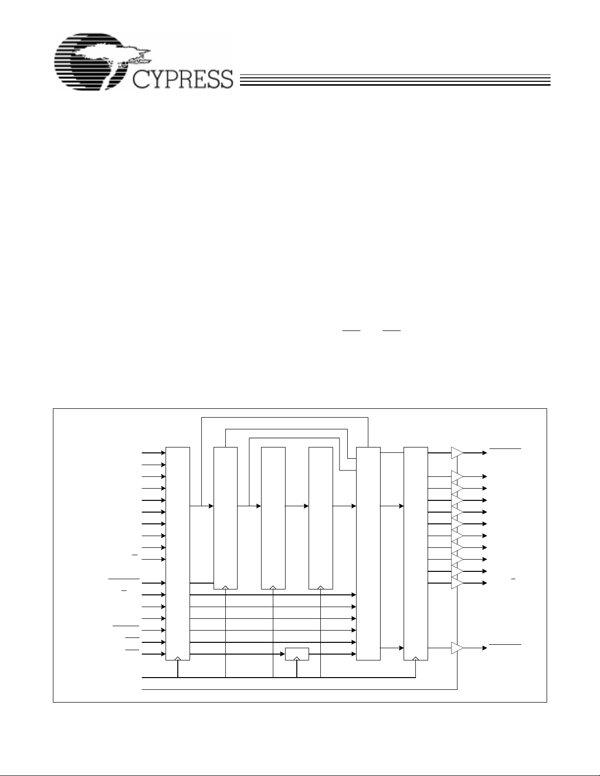
Logic Block Diagram
PD9(SVS)
PD
8
PD
7
PD
6
PD
5
PD
4
PD
3
PD
2
PD
PD0(SC/D)
1
TRS_FILT
SC/D_EN
SVS_EN
BYPASS
DVB_EN
ENA
ENN
CKW
OE
10
TRS FILTER / DETECTOR
INPUT REGISTER
10
10
10 10
NRZI ENCODER
SMPTE SCRAMBLER
MODE MULTIPLEXOR
OUTPUT REGISTER
TRS_DET
Q
(SVS)
9
Q
8
Q
7
Q
6
Q
5
Q
4
Q
3
Q
2
Q
1
Q0(SC/D)
ENA_OUT
Cypress Semiconductor Corporation
• 3901 North First Street • San Jose • CA 95134 • 408-943-2600
March 19
1999
PRELIMINARY
HOTLink is a trademark of Cypress Semiconductor Corporation.
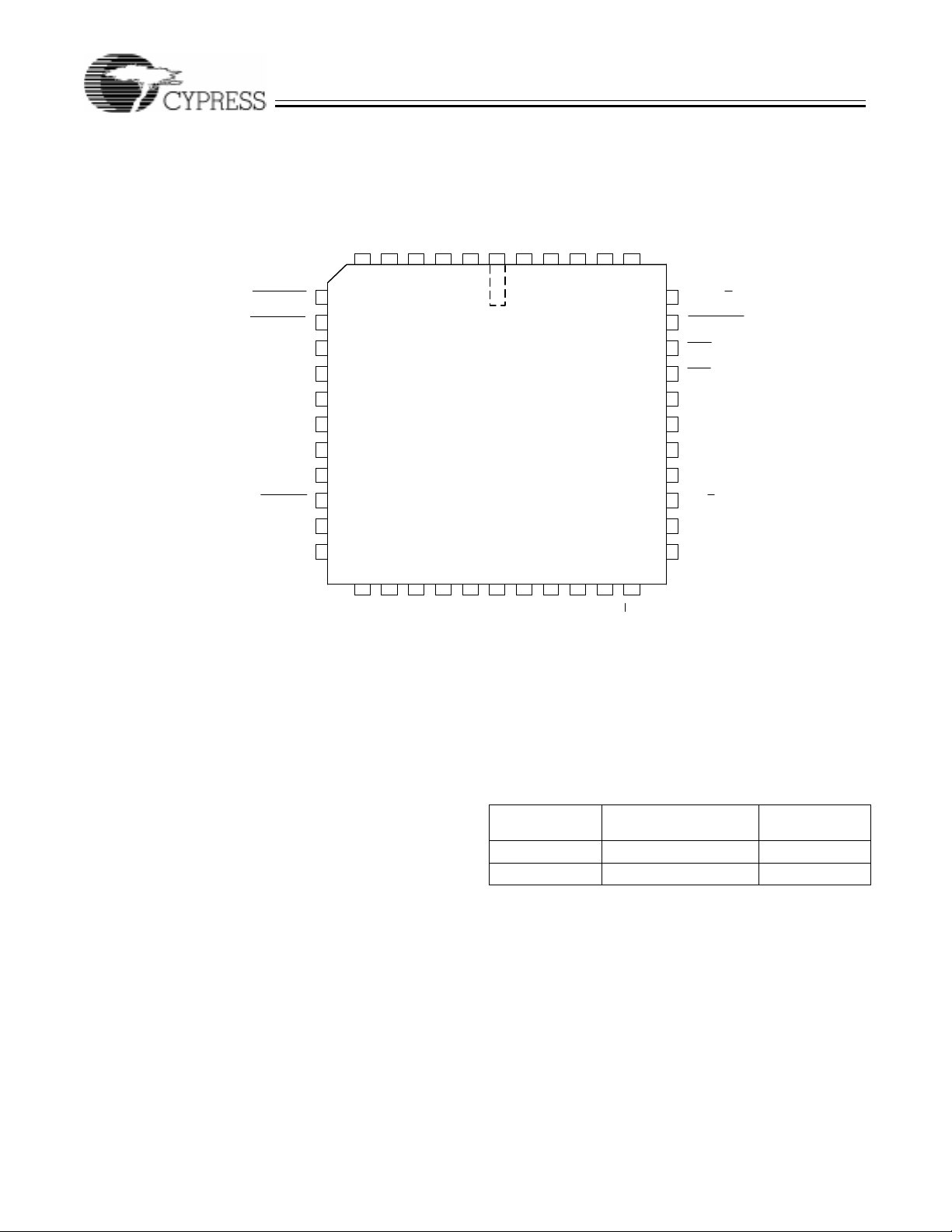
Pin Configuration
CY7C9235
Maximum Ratings
(SVS)
8
9
Q
Q
OE
NC
7
8
9
10
11
SS
12
SS
13
SS
14
15
16
17
NC
18 19 20 21 22 23 24 25 26 27 28
7
8
PD
PD
TRS_DET
TRS_FILT
SVS_EN
V
V
V
BYPASS
(SVS) NC
PD
9
5Q6Q7
V
Q
1444342414023456
PLCC
Top View
5PD6
CC
V
V
PD
CC
SS
V
SS
PD4PD3PD2PD
2Q3Q4
1
Q
Q
1
(SC/D)
0
PD
39
38
37
36
35
34
33
32
31
30
29
Q
(SC/D)
0
ENA_OUT
ENN
ENA
CKW
V
SS
V
SS
V
SS
SC/D_ENDVB_EN
NC
(Abov e which the useful lif e m ay be impaired. For user guidelines, not tested.)
Storage Temperature .....................................−40°C to +125°C
Supply Voltage to Ground Potential..................−0.5V to +7.0V
DC V oltage Applied to Outputs
in High-Z State.....................................................−0.5V to +7.0V
Output C ur re n t in to O u tp u ts.. .. ... .......... .. .......... .. ..........16 m A
DC Input Voltage.................................................−0.5V to +7.0V
Static Discharge Voltage.............................................. > 2001 V
(per MIL-STD-883, Method 3015)
DC Input Current.............................................................± 20 mA
Latch-Up Current............................................................>200 mA
Operating Range
Range
Commercial 0°C to +70°C 5V ± 5%
Industrial
Ambient
Temperature V
−40°C to +85°C
CC
5V ± 10%
2
PRELIMINARY
CY7C9235
Pin Descriptions
CY7C9235 SMPTE-259M Encoder
Name I/O Description
ENA Input Enable Parallel Data. If ENA is LOW at th e rising edge of CKW , the data prese nt on the PD
inputs is latched , and routed to the Q
active ( LOW). If the CY7C9235 is only used in SMPTE-259M mode this signal shoul d be ti ed
to V
.
SS
outputs. This pin is only interpreted when D VB_EN is
0–9
ENN Input Enable Next Parallel Data. If ENN is LOW at the rising edge of CKW, the data present on the
PD
inputs at t he next rising edge of TXCLK is latched, and routed to the Q
0–9
pin is only interpreted when DVB_EN
SMPTE-259M mode this signal should be tied to V
is active (LO W ). If the CY7C9235 is only used in
.
SS
outputs. This
0–9
BYPASS Input Bypass SMPTE Encoding. BYP ASS is ignore d if DVB_EN is act iv e (LO W). If BYPASS is HIGH
at the rising edge of CKW (and DVB_EN
is HIGH), the data latche d int o the input register is
routed around both the SMPTE scrambler and the NRZI encoder and presented to the output
register. If BYPASS is LOW at the rising edge of the CKW clock (and DVB_EN
is HIGH), the
data present in the in put register is routed th rough the SMPTE scrambler and NRZI encoder.
TRS_DET Output TRS Character Detect ed. This output indi cat es when a c haract er used i n the TRS s equen ce is
detected in the input register . If the data cont ains any of th e reserved characte rs of 000–003 or
3FC–3FF in 10- bi t he x, t he output will be LO W f or one cl oc k peri od. I f t he c haract er i n t he in put
register is any other pattern (or DVB_EN
is LOW) this output will remain HIGH.
TRS_FILT Input TRS Character Filter. This signal c ontrols an internal filter that con verts the low-o rder two bits
of all TRS char acters to same stat e as the upper eight bi ts. This al lows a pr oper 30-bit TRS ID
to be generated when t he CY7C9235 is operated with 8-bit or non-standard video st reams.
When this sig nal i s LO W, all characters f rom 00 0–003 are con v erted to 0 00, and a ll ch ar acters
from 3FC–3FF are converted to 3FF. When TRS_FILT
is disabled (HIG H), all characters are
passed to the scr ambler wit hout modifi cation. This si gnal has no eff ect when D VB_EN
(LOW).
SVS_EN Input Send Violation Symbol Enable. This input is only valid when DVB_EN is active (LOW). If
SVS_EN is HIGH and a HI GH input is pr esen t on PD
, Q9 will also be hi gh on a followi ng cloc k
9
cycle, forcing the CY7B9234 serializer to generate an invalid 8B/10B character. If SVS_EN is
LOW, the level present on PD
is ignored and Q9 is forced to a LO W st ate.
9
SC/D_EN Input Special Character /Data Sel ect Enab le. This input is only vali d when D VB_EN is active (LOW).
If SC/D
_EN is HIGH and a HIGH input is present on PD0, Q0 will also be high on a fo llowing
clock cycl e, f orcing the CY7B923 4 serializer to generate an 8B/ 10B control char acter as sele cted by the cha r acter p rese nt on t he PD
is ignored and Q
is forced to a LO W (data only) state.
0
inputs. If SC/D_EN i s LO W, the level pr esent on PD0
8–1
PD9(SVS) Input Parallel Data 9 or Send Violat ion Symbol. This is the MSB of the input dat a fi eld. It is latched
PD
8–1
in the input register at the rising edge of CKW. When DVB_EN
is HIGH, thi s latched inpu t is rout ed to the out put register bit Q
(LOW) and SVS _EN is L O W, output register b it Q
D VB_EN
is inactive (HIGH), this latched inp ut i s routed to the scrambl er and NRZI encoder.
(SVS) is forced t o a LOW (z ero) lev el. Wh en
9
Input Parallel Data 8 through 1. The signals present at the PD
register a t the risi ng edge of CKW. When DVB_EN
is HIGH, these s ignal s are the middle ei ght
is active (LOW) and SVS_EN
(SVS). When D VB_EN is act iv e
9
inputs are latched in the input
8–1
bits of the SMPTE 10-bit dat a fi eld, and are then routed to the scr am bler and NRZI encoder.
When DVB_EN
to the Q
is activ e (LOW), these signals are full DVB-ASI data bus, and are then r outed
outputs.
8−1
PD0(SC/D) Input Paral lel Data 0 or Sp ecial Code/Dat a Select . Thi s is th e LSB of the i nput data f iel d. It is lat ched
in the input register at the rising edge of CKW. When DVB_EN
is HIGH, thi s input is rout ed to output register bi t Q
SC/D
_EN is LOW , outpu t register bit Q0 (SC/D) is f orced t o a L OW (z ero) le v e l. When DVB_EN
(SVS). When D VB_EN is activ e (LO W) and
0
is active (LOW) and SC/D _EN
is inactiv e ( HIGH), this i nput d ata bit is r out ed thr ough the i npu t regist er and the s cram ble r an d
NRZI encoder.
Q9(SVS) Output Output Bit 9. This is the MSB of the out put register . It should be connecte d dir ectly to the
CY7B9234 serializer input signal SVS(Dj).
Q
8–1
Output Output Bits 8 through 1. These signals should be connect ed directly to the CY7B9234 serializer
input signal s D
respectively.
7−0
0−9
is activ e
3
 Loading...