

Datasheet CY7C68013-56PVC, CY7C68013-56LFC, CY7C68013-128AC, CY7C68013-100AC Datasheet (Cypress Semiconductor)

CY7C68013
CY7C68013
EZ-USB FX2™ USB Microcontroller
High-speed USB Peripheral Controller
Cypress Semiconductor Corporation • 3901 North First Street • San Jose, CA 95134 • 408-943-2600
Document #: 38-08012 Rev. *C Revised December 19, 2002

CY7C68013
TABLE OF CONTENTS
1.0 EZ-USB FX2™ FEATURES ............................................................................................................. 6
2.0 APPLICATIONS ...............................................................................................................................7
3.0 FUNCTIONAL OVERVIEW ............ .. .. .. .. .................................... .. .. .. .................................... .. .. ........7
3.1 USB Signaling Speed ........................................................................................ .. .......................7
3.2 8051 Microprocessor ................ .. .................... .. .................... ........................................ .. ............7
2
3.3 I
C-compatible Bus .....................................................................................................................8
3.4 Buses ..........................................................................................................................................8
3.5 USB Boot Methods .....................................................................................................................9
3.6 ReNumeration™ ......................................................................................................................... 9
3.7 Bus Powered Applications ..........................................................................................................9
3.8 Interrupt System ........................................................................................................................10
3.9 Reset and Wakeup ....................... .................... .. .................... .. .................... .. ..........................11
3.10 Program/Data RAM .................................................................................................................11
3.11 Register Addresses .................................................................................................................14
3.12 Endpoint RAM .......................................... .. ............................................. ................................ 14
3.13 Externa l F IF O in te rface ............................................... .......................................... ..................16
3.14 GPIF ........................................................................................................................................16
3.15 USB Uploads and Downloads ............................. .. ......................... .. .. .. ......................... .. ........17
3.16 Autopointer Access .................................................. .. ...................... .. ...................... ...............17
2
3.17 I
C-compatible Controller ........................................................................................................17
4.0 PIN ASSIGNMENTS .............................. .................... .. .................... .. .................... ........................18
4.1 CY7C68013 Pin Descriptions .................. .............................................................. ...................24
5.0 REGISTER SUMMARY ..................................... ........................................... .. .. ..............................31
6.0 ABSOLUTE MAXIMUM RATINGS ................................................................................................37
7.0 OPERATING CONDITIONS .................................................. .. .................... .................... .. .............37
8.0 DC CHARACTERISTICS ................................ .. ........................... .. .. .. ........................... .. .. .............37
8.1 USB Transceiver .......................................................................................................................37
9.0 AC ELECTRICAL CHARACTERISTICS ........... .. .................... .. .................... .. .................... ..........38
9.1 USB Transceiver .......................................................................................................................38
9.2 Program Memory Read ............................ .. ................................................. .. ............................38
9.3 Data Memory Read ................... .. ...................... .. .. ............................................ ........................39
9.4 Data Memory Write ...................................................................................................................40
9.5 GPIF Synchronous Signals ........................................................... ................................ ............41
9.6 Slave FIFO Synchronous Read ..................................................................................... ...........42
9.7 Slave FIFO A s y nc h r o no u s R e ad ..............................................................................................43
9.8 Slave FIFO Synchronous Write ..................... ................................. ..........................................43
9.9 Slave FIFO Asynchronous W rite ......... ............... .......................................................................44
9.10 Slave FIFO Synchronous Packet End Strobe .........................................................................44
9.11 Slave FIFO Asynchronous Packet End Strobe .......................................................................45
9.12 Slave FIFO Output Enable ......................................................................................................45
9.13 Slave FIFO A d d re s s to F la g s /D a t a ......... ................ .......................................... ......................45
9.14 Slave FIFO S y n ch r o n ou s A d d re s s ............................ .......................................... ....................46
9.15 Slave FIFO Asynchronous Address ................................... .....................................................46
Document #: 38-08012 Rev. *C Page 2 of 52

CY7C68013
10.0 ORDERING INFORMATION ................................................................. .. .. ............................... ....46
11.0 PACKAGE DIAGRAMS ............................................. .................................... .. .. ..........................47
12.0 PCB LAYOUT RECOMMENDATIONS ......................... .. .. .. .. ................................ .. .. .. .. .. .............50
13.0 QUAD FLAT PACKAGE NO LEADS (QFN) PACKAGE DESIGN NOTES .................... .. ..........50
Document #: 38-08012 Rev. *C Page 3 of 52

CY7C68013
LIST OF FIGURES
Figure 1-1. Blo c k Di a gr a m .......................... .......................................... ...................................................6
Figure 3-1. Internal Code Memory, EA = 0........................... ....................................... .. .................. ......12
Figure 3-2. External Code Memory, EA = 1................................ .................. .................... .....................13
Figure 3-3. Endpoint Configuration........................................................................................................15
Figure 4-1. Signals.................................................................................................................................19
Figure 4-2. CY7C68013 128-pin TQFP Pin Assignment.......................................................................20
Figure 4-3. CY7C68013 100-pin TQFP Pin Assignment.......................................................................21
Figure 4-4. CY7C68013 56-pin SSOP Pin Assignment.........................................................................22
Figure 4-5. CY7C68013 56-pin QFN Pin Assignment.......................................... .................................23
Figure 9-1. Pro g r a m M e m o ry R ead T i ming Diagram.... .. .......................................................................38
Figure 9-2. Data Memory Read Timing Diagram...................................................................................39
Figure 9-3. Data M e m o r y Wr ite T im ing Diagram......................................... ............................ .............. 40
Figure 9-4. GPIF Synchronous Signals Timing Diagram .......................................................................41
Figure 9-5. Slave FIFO Synchronous Read Timing Diagram...................................... .. ........................42
Figure 9-6. Slave FIFO Asynchronous Read Timing Diagram ..............................................................43
Figure 9-7. Slave FIFO Synchronous Write Timing Diagram ........................... .. ...................... .............43
Figure 9-8. Slave FIFO Asynchronous Write Timing Diagram...................... .. .......................................44
Figure 9-9. Slave FIFO Synchronous Packet End Strobe Timing Diagram...........................................44
Figure 9-10. Slave FIFO Asynchronous Packet End Strobe Timing Diagram.......................................45
Figure 9-11. Slave FIFO Output Enable Timing Diagram......................................................................45
Figure 9-12. Slave FIFO Address to Flags/Data Timing Diagram ......................................................... 45
Figure 9-13. Slave FIFO Synchronous Address Timing Diagram..........................................................46
Figure 9-14. Slave FIFO Asynchronous Address Timing Diagram................................... .....................46
Figure 11-1. 56-lead Shrunk Small Outline Package O56.................................... .................................47
Figure 11-2. 56-lead Quad Flatpack No Lead Package (8 × 8 mm) LF56................................ .............47
Figure 11-3. 100-Pin Thin Plastic Quad Flatpack (14 × 20 × 1.4 mm) A101 .........................................48
Figure 11-4. 128-Lead Thin Plastic Quad Flatpack (14 × 20 × 1.4 mm) A128 ......................................49
Figure 13-1. Cross-section of the Area Underneath the QFN Package ................................................50
Figure 13-2. P lo t of th e S o ld e r Ma s k (White Area)............. ... ............... .......................................... .......50
Figure 13-3. X -r a y im ag e o f th e as s e mb ly................................................ .............................................51
Document #: 38-08012 Rev. *C Page 4 of 52

CY7C68013
LIST OF TABLES
Table 3-1. Special Function Registers ................................. ..................... .................... ..........................9
Table 3-2. Default ID Values for FX2 ................... .. .................... .. .................... .. .....................................9
Table 3-3. INT2 USB Interrupts ................................................... ...................... .................... ...............10
Table 3-4. Individual FIFO/GPIF Interr upt Sources .......... .. ..................................................................11
Table 3-5. Default Full-Speed Alternate Setti ngs ................................... .................... .. ........................15
Table 3-6. Default High-Speed Alternate Settings .......................................................... ......................16
Table 3-7. Strap Boot EEPROM Address Lines to These Values ........................................... .............18
Table 4-1. FX2 Pin Descriptions ............................ ................................. ................ ..............................24
Table 5-1. FX2 Register Summary ............................... .................... .................... .................... ............31
Table 8-1. DC Characteristics ................... .................... .................... .................... ................................37
Table 9-1. Program Memory Read Parameters ............................................. .. .................... .. ...............38
Table 9-2. Data Memory Read Parameters .................... .. ........................................ .................... .. ......39
Table 9-3. Data Memory Write Parameters ............................... ..................................................... ......40
Table 9-4. GPIF Synchronous Signals Parameters with Internally Sourced IFCLK .............................41
Table 9-5. GPIF Synchronous Signals Parameters wit h Externally Sourced IFCLK ............................41
Table 9-6. Slave FIFO Synchronous Read Parameters with Internally Sourced IFCLK .......................42
Table 9-7. Slave FIFO Synchronous Read Parameters with Externally Sourced IFCLK .....................42
Table 9-8. Slave FIFO Asynchronous Read Parameters ............................................. .................... .. ..43
Table 9-9. Slave FIFO Synchronous Write Parameters with Internally Sourced IFCLK .......................43
Table 9-10. Slave FIFO Synchronous Write Parameters with Externally Sourced IFCLK ....................44
Table 9-11. Slave FIFO Asynchronous Write Parameters wi th Internally Sourced IFCLK ............. .. ....44
Table 9-12. Slave FIFO Synchronous Packet End Strobe Parameters with Internally Sourced IFCLK 44
Table 9-13. Slave FIFO Synchronous Packet End Strobe Parameters with Externally Sourced IFCLK 45
Table 9-14. Slave FIFO Asynchronous Packet End Strobe Parameters ............................... ...............45
Table 9-15. Slave FIFO Output Enable Parameters ........................................................ .. ...................45
Table 9-16. Slave FIFO Address to Flags/Data Parameters ....................... .. .................. .. .................. .46
Table 9-17. Slave FIFO Synchronous Address Parameters .................................................................46
Table 9-18. Slave FIFO Asynchronous Address Parameters ............................... ................................46
Table 10-1. Ordering Information ................................ ....................................... .................. .................46
Document #: 38-08012 Rev. *C Page 5 of 52
CY7C68013
1.0 EZ-USB FX2 Features
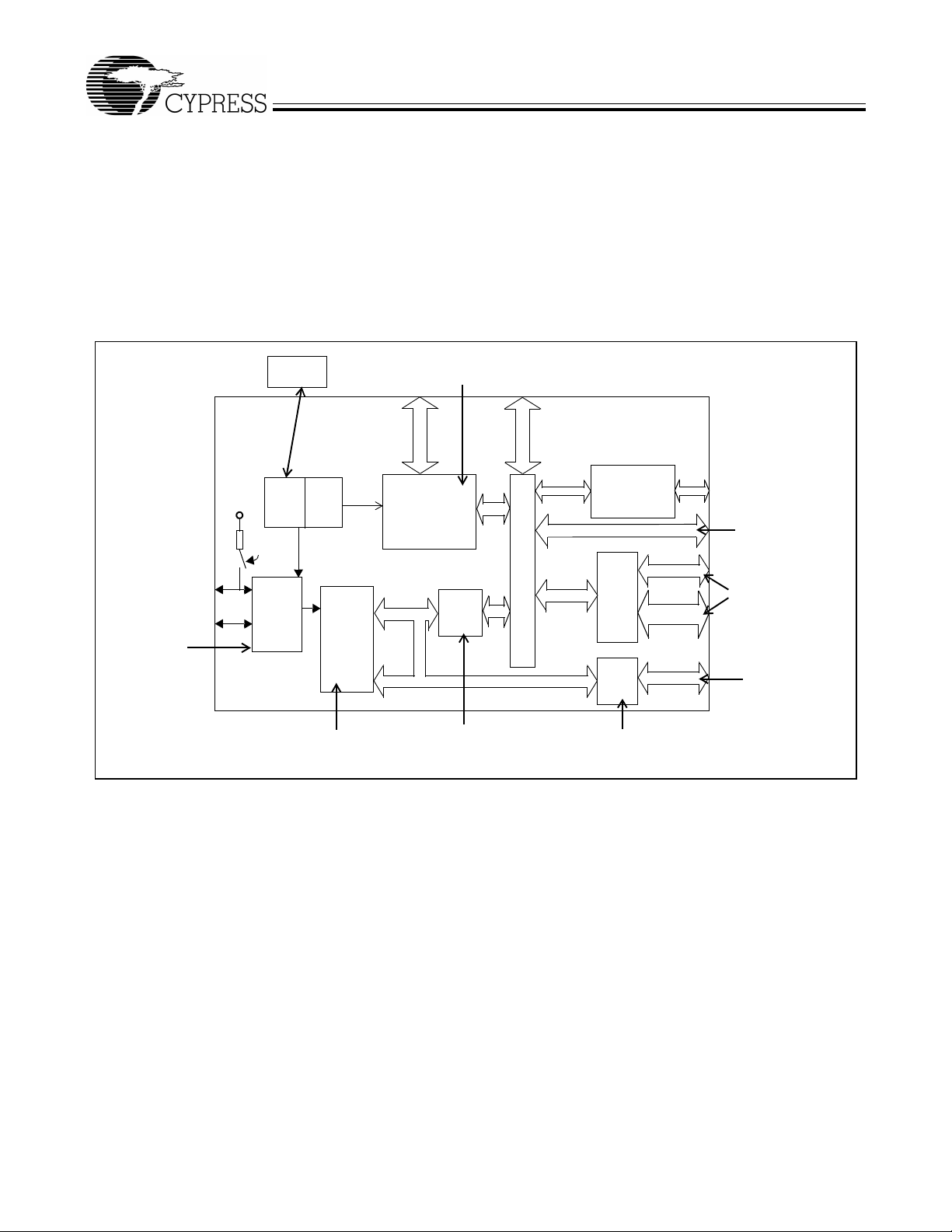
Cypress’s EZ-USB FX2 is the world’s first USB 2.0 integrated microcontroller. By integrating the USB 2.0 transceiver, SIE,
enhanced 805 1 microcontroll er, and a programmable peri pheral interfac e in a single chip, Cypr ess has created a ver y costeffective solution that provides superior time-to-market advantages. The ingenious architecture of FX2 results in data transfer
rates of 56 Mbytes per second, the maximum allowable USB 2.0 bandwidth, while still using a low-cost 8051 microcontroller in
a package as small as a 56 SSOP. Because it incorporates the USB 2.0 transceiver, the FX2 is more economical, providing a
smaller footprint solution than USB 2.0 SIE or external transceiver implementations. With EZ-USB FX2, the Cypress Smart SIE
handles most of th e USB 1.1 and 2 .0 protocol in hardware, freeing th e embedded micr ocontroller fo r application-spec ific functions
and decreasing development time to ensure USB compatibility. The General Programmable Interface (GPIF) and Master/Slave
Endpoint FIFO (8- or 16- bit data bus) provides an easy and glue les s int erfa ce to p op ula r in terfaces such as
PCMCIA, and most DSP/processors.
Four packages are defined for the family: 56 SSOP, 56 QFN, 100 TQFP, and 128 TQFP.
24 MHz
Ext. XTAL
High-performance micro
using standard tools
with lower-power options
FX2
ATA, UTOPIA, EPP,
Data (8)
Compatible
Additional I/Os (24)
GPIF
Address (16) / Data Bus (8)
4 kB
FIFO
FIFO and endpoint memory
(master or slave operation)
2
I
C
Master
ADDR (9)
Integrated
full- and high-speed
XCVR
D+
D–
x20
V
CC
PLL
1.5k
connected for
full speed
USB
2.0
XCVR
Enhanced USB core
Simplifies 8051 core
/0.5
/1.0
/2.0
CY
Smart
USB
1.1/2.0
Engine
Address (16)
8051 Core
12/24/48 MHz,
four clocks/cycle
8.5 kB
RAM
“Soft Configuration”
Easy firmware changes
Figure 1-1. Block Diagram
• Single-chip integrated USB 2.0 Transceiver, SIE, and Enhanced 8051 Microprocessor
• Software: 8051 runs from internal RAM, which is:
—Downloaded via USB, or
—Loaded from EEPROM
—External memory device (128-pin configuration only)
• Four programmable BULK/INTERRUPT/ISOCHRONOUS endpoints
—Buffering options: double, triple and quad
• 8- or 16-bit external data interface
• GPIF
—Allows direct connection to most parallel interfaces; 8- and 16-bit
—Programmable waveform descriptors and configuration registers to define waveforms
—Supports multiple Ready (RDY) inputs and Control (CTL) outputs
• Integrated, industry standard 8051 with enhanced features:
—Up to 48-MHz clock rate
—Four clocks per instruction cycle
—Two USARTS
RDY (6)
CTL (6)
8/16
Abundant I/O
including two USARTS
General
programmable I/F
to ASIC/DSP or bus
standards such as
ATAPI, EPP, etc.
Up to 96 MBytes/s
burst rate
Document #: 38-08012 Rev. *C Page 6 of 52

—Three counter/timers
—Expanded interrupt system
—Two data pointers
• Supports bus powered applications by using renumeration
• 3.3V operation
• Smart Serial Interface Engine
• Vectored USB interrupts
• Separate data buffers for the SETUP and DATA portions of a CONTROL transfer
• Integrated I
• 48-MHz, 24-MHz, or 12-MHz 8051 operation
• Four integrated FIFOs
—Brings glue and FIFOs inside for lower system cost
—Automatic conversion to and from 16-bit buses
—Master or slave operation
—FIFOs can use externally supplied clock or asynchronous strobes
—Easy interface to ASIC and DSP ICs
• Special autovectors for FIFO and GPIF interrupts
• Up to 40 general purpose I/Os
• Four package options—128-pin TQFP, 100-pin TQFP, 56-pin QFN and 56-pin SSOP.
2
C-compatible controller, runs at 100 or 400 kHz
2.0 Applications
CY7C68013
• DSL modems
• ATA interface
• Memory card readers
• Legacy conversion devices
• Cameras
• Scanners
• Home PNA
• Wireless LAN
• MP3 players
• Networking.
The “Reference Designs” section of the c ypress website provides additio nal tools for ty pical USB 2.0 app lications. Eac h reference
design comes complete with firmware source and object code, schematics, and documentation. Please visit
http://www.cypress.com for more information.
3.0 Functional Overview
3.1 USB Signaling Speed
FX2 operates at two of the three rates defined in the Universal Serial Bus Specification Revision 2.0, dated April 27, 2000:
• Full speed, with a signaling bit rate of 12 Mbps
• High speed, with a si gnaling bit rate of 480 Mbps
FX2 does not support the low-speed signaling mode of 1.5 Mbps.
3.2 8051 Microprocessor
The 8051 microprocessor embedded in the FX2 family has 256 bytes of register RAM, an expanded interrupt system, three
timer/counters, and two USARTs.
Document #: 38-08012 Rev. *C Page 7 of 52

CY7C68013
3.2.1 8051 Clock Frequency
FX2 has an on-chip oscillator circuit that uses an external 24-MHz (±100 ppm) crystal with the following characteristics:
• Parallel resonant
• Fundamental mode
• 500-µW drive level
• 20–33 pF (5% tolerance) load capacitors.
An on-chip PLL multiplies the 24-MH z oscill ator up to 48 0 MHz, as requi red by the trans ceive r/PHY, and internal counter s divide
it down for use as the 80 51 cloc k. The defau lt 8051 cloc k freq uency is 1 2 MHz. The c lock frequen cy o f the 8051 can b e cha nged
by the 8051 through the CPUCS register, dynamically.
The CLKOUT pin, which can be tri-stated and inverted using internal control bits, outputs the 50% duty cycle 8051 clock, at the
selected 8051 clock frequency—48, 24, or 12 MHz.
3.2.2 USARTS
FX2 contains two standard 8051 USARTs, addressed via Special Function Register (SFR) bits. The USART interface pins are
available on separate I/O pins, and are not multiplexed with port pins.
UART0 and UAR T1 can operate using an internal clock at 230 KBaud with no more than 1% ba ud rate error . 230-KBaud operation
is achieved by an internally deriv ed clock sour ce that generates overflow pulses at the appropriat e time. The intern al clock ad justs
for the 8051 clock rate (48, 24, 12 MHz) such that it always presents the correct frequency for 230-KBaud operation.
Note. 1 15-KBau d operatio n is also p ossible by programm ing the 8 051 SMOD0 or SMOD 1 bits to a “1” fo r UART 0 and/or UA RT1,
respectively.
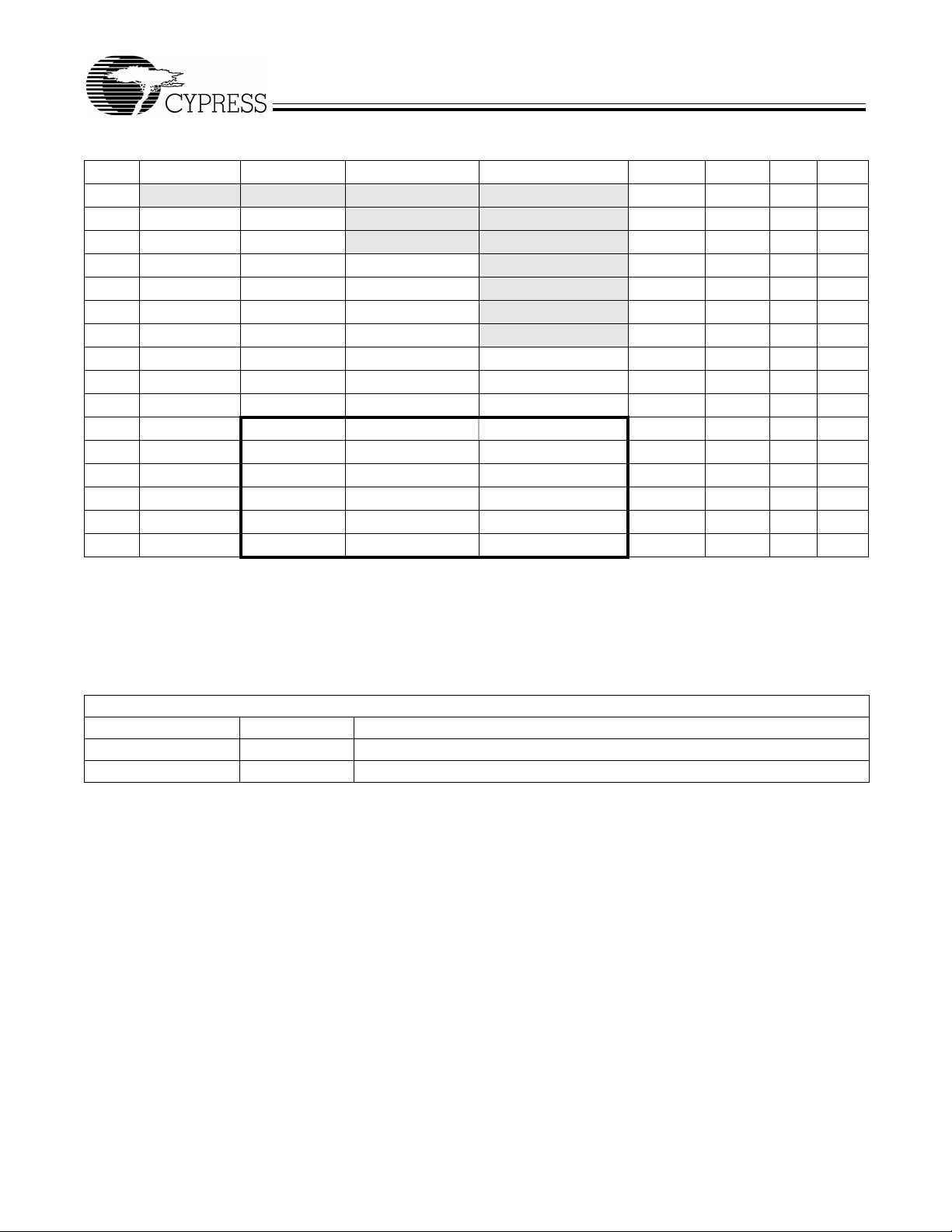
3.2.3 Special Function Registers
Certain 8051 SFR addresses are populated to provide fast access to critical FX2 functions. These SFR additions are shown in
Table 3-1. Bold type indicates non-standard, enhanced 8051 registers.
The two SFR rows that end with “0” and “8” contain bit-addressable registers. The four I/O ports A–D use the SFR addresses
used in the standard 8051 for ports 0–3, which are not implemented in FX2.
Because of the faster and more efficient SFR addressing, the FX2 I/O ports are not addressable in external RAM space (using
the MOVX instruction).
3.3 I2C-compatible Bus
FX2 supports the I2C-compatible bus as a master only at 100/400 kbps. SCL and SDA pins have open-drain outputs and
hysteresis inputs. These signals must be pulled up to 3.3V, even if no I
2
C-compatible device is connected.
3.4 Buses
All packages: 8- or 16-bit “FIFO” bidirectional data bus, multiplexed on I/O ports B and D. 128-pin package: adds 16-bit outputonly 8051 address bus, 8-bit bidirectional data bus.
Document #: 38-08012 Rev. *C Page 8 of 52
CY7C68013
Table 3-1. Special Function Registers
x8x 9x Ax Bx CxDxExFx
0
1SP EXIF
2DPL0 MPAGE
3DPH0
4 DPL1
5 DPH1
6 DPS
7PCON
8 TCON SCON0 IE IP T2CON EICON EIE EIP
9 TMOD SBUF0
ATL0AUTOPTRH1 EP2468STAT EP01STAT RCAP2L
BTL1AUTOPTRL1 EP24FIFOFLGS GPIFTRIG RCAP2H
CTH0reserved EP68FIFOFLGS TL2
DTH1AUTOPTRH2 GPIFSGLDATH TH2
E CKCON AUTOPTRL2 GPIFSGLDATLX
F reserved AUTOPTRSETUP GPIFSGLDATLNOX
IOA IOB IOC IOD SCON1 PSW ACC B
INT2CLR IOE SBUF1
INT4CLR OEA
OEB
OEC
OED
OEE
3.5 USB Boot Methods
During the power-u p s equ en ce, in ternal logic checks the I2C-compatible port for the connection of an EEPROM whose first byte
is either 0xC0 or 0xC2. If found, it uses the VID/PID/DID values in the EEPROM in place of the internally stored values (0xC0),
or it boot-loads the EEPROM contents into internal RAM (0xC2). If no EEPROM is detected, FX2 enumerates using internally
stored descriptors. The default ID values for FX2 are VID/PID/DID (0x04B4, 0x8613, 0xxxyy).
Table 3-2. Default ID Values for FX2
Default VID/PID/DID
Vendor ID 0x04B4 Cypress Semiconductor
Prod ID 0x8613 EZ-USB FX2
Device release 0xXXYY Depends on revision (0x04 for Rev E)
2
Note. The I
detection method does not work properly.
3.6 ReNumeration
Because the FX2’s configuration is soft, one chip can take on the identities of multiple distinct USB devices.
When first plugged into USB, the FX2 enumerates automatically and downloads firmware and USB descriptor tables over the
USB cable. Next, the FX2 enumerates again, this time as a device defined by the downloaded information. This patented twostep process, called ReNumeration
has occurred.
Two control bits in the USBCS (USB Control and Status) register control the ReNumeration process: DISCON and RENUM. To
simulate a USB disconnect, the firmware sets DISCON to 1. To reconnect, the firmware clears DISCON to 0.
Before reconnecting, the fi rmwa re se t s or clears the RENUM bi t to in dic at e wheth er the firmware o r t he Defa ul t USB Device wil l
handle device requests over endpoint zero: if RENUM = 0, the Default USB Device will handle device requests; if RENUM = 1,
the firmware will.
C-compatible bus SCL and SDA pins must be pulled up, even if an EEPROM is not connected. Otherwise this
™
™
, happens instantl y when the dev ice is plugged in, with no hint tha t the in itial down load ste p
3.7 Bus Powered Applications
Bus powered applicat ions requi re the FX2 to enum erate in a un configure d mode with le ss then 100 mA. To do this, the FX2 must
enumerate in the full speed mode and then, when configured, renumerate in high speed mode. For an example of the benefits
and limitations of this renumeration process see the application note titled “Bus Powered Enumeration with FX2”.
Document #: 38-08012 Rev. *C Page 9 of 52
CY7C68013
3.8 Interrupt System
3.8.1 INT2 Interrupt Request and Enable Registers
FX2 implements an autovector feature for INT2 and INT4. There are 27 INT2 (USB) vectors, and 14 INT4 (FIFO/GPIF) vectors.
See FX2 TRM for more details.
3.8.2 USB-Interrupt Autovectors
The main USB interrupt is sh ared by 27 interru pt sources . To save the code and processi ng time that normally wou ld be required
to identify the individual USB interrupt source, the FX2 p rovides a second l evel of interrupt vec toring, c alled Aut ovectorin g. When
a USB interrupt is asse rted, the FX2 pushes the program counter onto its stack then jumps to addres s 0x0043, where it expects
to find a “jump” instruction to the USB Interrupt service routine.
The FX2 jump instruction is encoded as follows.
Table 3-3. INT2 USB Interrupts
USB INTERRUPT TABLE FOR INT2
Priority INT2VEC Value Source Notes
1 00 SUDAV SETUP Data Available
2 04 SOF Start of Frame (or microframe)
3 08 SUTOK Setup Token Received
4 0C SUSPEND USB Suspend request
5 10 USB RESET Bus reset
6 14 HISPEED Entered high speed operation
7 18 EP0ACK FX2 ACK’d the CONTROL Handshake
8 1C reserved
9 20 EP0-IN EP0-IN ready to be loaded with data
10 24 EP0-OUT EP0-OUT has USB data
11 28 EP1-IN EP1-IN ready to be loaded with data
12 2C EP1-OUT EP1-OUT has USB data
13 30 EP2 IN: buffer available. OUT: buffer has data
14 34 EP4 IN: buffer available. OUT: buffer has data
15 38 EP6 IN: buffer available. OUT: buffer has data
16 3C EP8 IN: buffer available. OUT: buffer has data
17 40 IBN IN-Bulk-NAK (any IN endpoint)
18 44 reserved
19 48 EP0PING EP0 OUT was Pinged and it NAK’d
20 4C EP1PING EP1 OUT was Pinged and it NAK’d
21 50 EP2PING EP2 OUT was Pinged and it NAK’d
22 54 EP4PING EP4 OUT was Pinged and it NAK’d
23 58 EP6PING EP6 OUT was Pinged and it NAK’d
24 5C EP8PING EP8 OUT was Pinged and it NAK’d
25 60 ERRLIMIT Bus errors exceeded the programmed limit
26 64 reserved
27 68 reserved
28 6C reserved
29 70 EP2ISOERR ISO EP2 OUT PID sequence error
30 74 EP4ISOERR ISO EP4 OUT PID sequence error
31 78 EP6ISOERR ISO EP6 OUT PID sequence error
32 7C EP8ISOERR ISO EP8 OUT PID sequence error
Document #: 38-08012 Rev. *C Page 10 of 52
CY7C68013
If Autovectoring is enabled (AV2EN = 1 in the INTSETUP register), the FX2 substitutes its INT2VEC byte. Therefore, if the high
byte (“page”) of a jump-table address is preloaded at location 0x0044, the automatically-inserted INT2VEC byte at 0x0045 will
direct the jump to the correct address out of the 27 addresses within the page.
3.8.3 FIFO/GPIF Interrupt (INT4)
Just as the USB Interrupt is shared among 27 individual USB-interrupt sources, the FIFO/GPIF interrupt is shared among 14
individual FIFO/GPIF sources. The FIFO/GPIF Interrupt, like the USB Interrupt, can employ autovectoring. Table 3-4 shows the
priority and INT4VEC values for the 14 FIFO/GPIF interrupt sources
Table 3-4. Individual FIFO/GPIF Interrupt Sources
Priority INT4VEC Value Source Notes
1 80 EP2PF Endpoint 2 Programmable Flag
2 84 EP4PF Endpoint 4 Programmable Flag
3 88 EP6PF Endpoint 6 Programmable Flag
4 8C EP8PF Endpoint 8 Programmable Flag
5 90 EP2EF Endpoint 2 Empty Flag
6 94 EP4EF Endpoint 4 Empty Flag
7 98 EP6EF Endpoint 6 Empty Flag
8 9C EP8EF Endpoint 8 Empty Flag
9 A0 EP2FF Endpoint 2 Full Flag
10 A4 EP4FF Endpoint 4 Full Flag
11 A8 EP6FF Endpoint 6 Full Flag
12 AC EP8FF Endpoint 8 Full Flag
13 B0 GPIFDONE GPIF Operation Complete
14 B4 GPIFWF GPIF Waveform
If Autovectoring is enabled (AV4EN = 1 in the INTSETUP register), the FX2 substitutes its INT4VEC byte. Therefore, if the high
byte (“page”) of a jump-table address is preloaded at location 0x0054, the automatically-inserted INT4VEC byte at 0x0055 will
direct the jump to the correct address out of the 14 address es within the page . When the ISR occurs, the FX2 p ushes the program
counter onto its stack then jumps to address 0x0053, where it expects to find a “jump” instruction to the ISR Interrupt service
routine.
3.9 Reset and Wakeup
3.9.1 Reset Pin
An input pin (RESET#) reset s th e chi p. This pin has h ysteresi s and is a ctive LO W. The internal PLL stabil izes approxim ately 200
µs after V
3.9.2 Wakeup Pins
The 8051 puts itself and the rest of the chip into a power-down mode by setting PCON.0 = 1. This stops the oscillator and PLL.
When WAKEUP is asserted by e xternal logic , the osc illator res tarts and after th e PLL stabi lizes, a nd the 8051 receives a wak eup
interrupt. This applies whether or not FX2 is connected to the USB.
The FX2 exits the power down (USB suspend) state using one of the following methods:
• USB bus signals resume
• External logic asserts the WAKEUP pin
• External logic asserts the PA3/WU2 pi n.
The second wakeup pin, WU2, can also be configured as a general purpose I/O pin. This allows a simple external R-C network
to be used as a periodic wakeup source.
has reached 3.3V. Typically, an external RC network (R = 100k, C = 0.1 µF) is used to provide the RESET# signal.
CC
3.10 Program/Data RAM
3.10.1 Size
The FX2 has eight kbytes of internal program/data RAM, where PSEN#/RD# signals are internally ORed to allow the 8051 to
access it as both program and data memory. No USB control registers appear in this space.
Document #: 38-08012 Rev. *C P age 11 of 52
CY7C68013
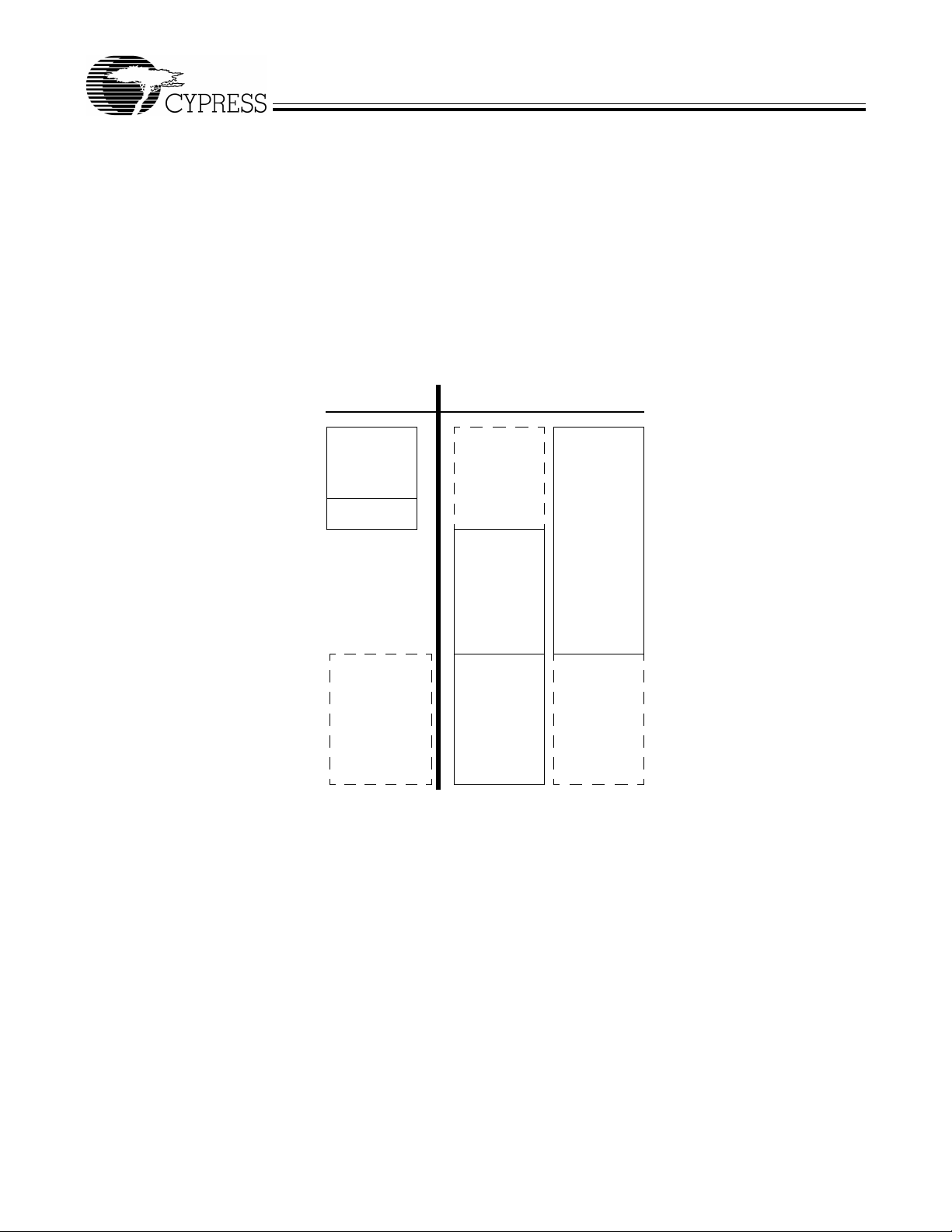
Two memory maps are shown in the following diagrams:
Figure 3-1 Internal Code Memory, EA = 0
Figure 3-2 External Code Memory, EA = 1.
3.10.2 Internal Code Memory, EA = 0
This mode implement s the in tern al ei ght-kbyte block of RAM (starting at 0) as combined code and data memory. When external
RAM or ROM is added, the external read and write strobes are suppressed for memory spaces that exist inside the chip. This
allows the user to connect a 64-kbyte memory without requiring address decodes to keep clear of internal memory spaces.
Only the internal eight kbytes and scratch pad 0.5 kbytes R AM spaces have the following access:
• USB download
• USB upload
• Setup data pointer
2
• I
C-compatible interface boot load.
Inside FX2 Outside FX2
FFFF
E200
E1FF
0.5 kbytes RAM
Data (RD#,WR#)*
E000
7.5 kbytes
US B regs and
4k EP buffers
(RD#,WR#)
(OK to populate
data memory
here—RD#/WR#
strobes are not
active)
48 kbytes
External
Data
Memory
(RD#,WR#)
56 kbytes
External
Code
Memory
(PSEN#)
1FFF
Eight kbytes RAM
Code and Data
(PSEN#,RD#,WR#)*
0000
(Ok to populate
data memory
here—RD#/WR#
strobes are not
active)
Data Code
(OK to populate
program
memory here—
PSEN# strobe
is not active)
*SUDPTR, USB upload/download, I2C-compatible interface boot access
Figure 3-1. Internal Code Memory, EA = 0
Document #: 38-08012 Rev. *C Page 12 of 52
CY7C68013
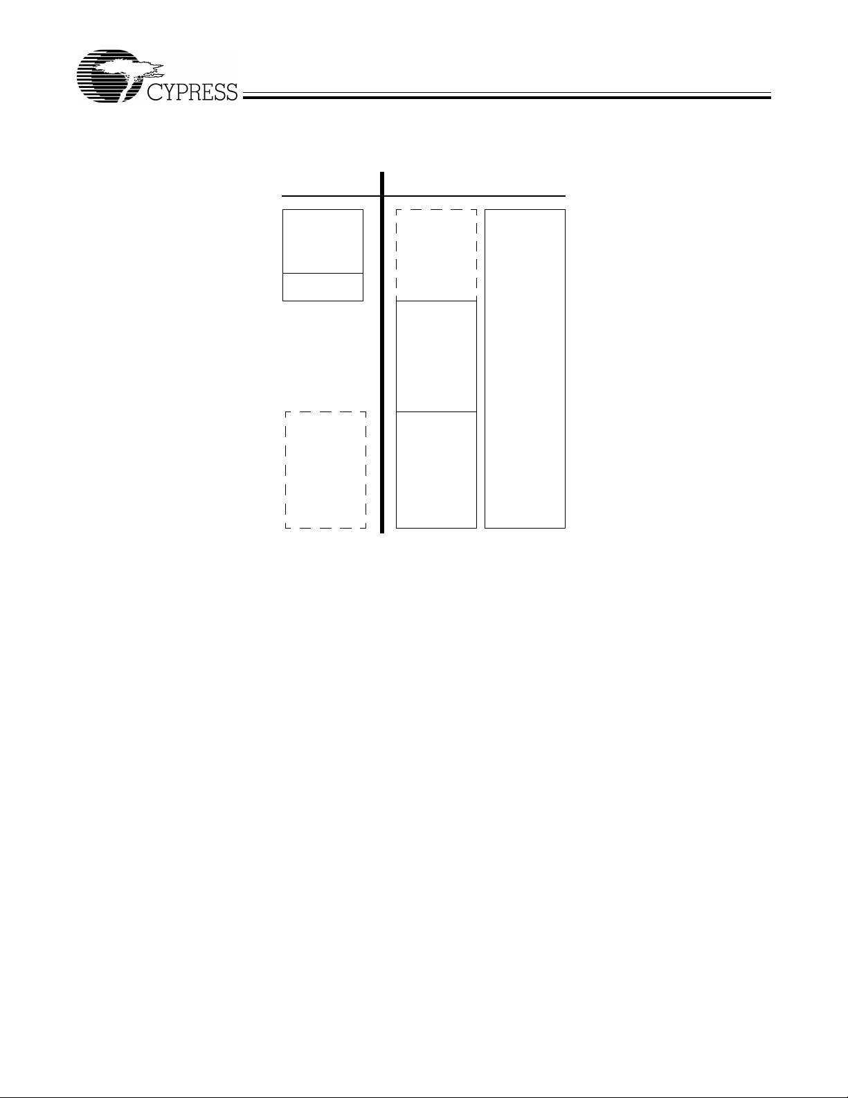
3.10.3 External Code Memory, EA = 1
The bottom eight k bytes of pr ogram me mory is exte rnal, and th erefore the bottom ei ght kbytes of int ernal RAM is access ible onl y
as data memory.
Inside FX2 Outside FX2
FFFF
E200
E1FF
0.5 kbytes RAM
Data (RD#,WR#)*
E000
1FFF
7.5 kbytes
USB regs and
4k EP buffers
(RD#,WR#)
(OK to populate
data memory
here—RD#/WR#
strobes are not
active)
48 kbytes
External
Data
Memory
(RD#,WR#)
64 kbytes
External
Code
Memory
(PSEN#)
(Ok to populate
data memory
here—RD#/WR#
strobes are not
active)
Data Code
0000
Eight kbytes
RAM
Data
(RD#,WR#)*
*SUDPTR, USB upload/download, I2C-compatible interface boot access
Figure 3-2. External Code Memory, EA = 1
Document #: 38-08012 Rev. *C Page 13 of 52

3.11 Register Addresses
FFFF
4 kbytes EP2-EP8 buffers
F000
EFFF
2 kbytes RESERVED
E800
E7FF
E7C0
E7BF
E780
E77F
E740
E73F
E700
E6FF
E600
E5FF
E480
E47F
E400
E3FF
E200
E1FF
E000
64 bytes EP1IN
64 bytes EP1OUT
64 bytes EP0 IN/OUT
64 bytes RESERVED
256 bytes Registers
384 bytes RESERVED
128 bytes GPIF Waveforms
512 bytes RESERVED
(8 × 512)
512 bytes
8051 xdata RAM
CY7C68013
3.12 Endpoint RAM
3.12.1 Size
• 3 × 64 bytes (Endpoints 0 and 1)
• 8 × 512 bytes (Endpoints 2, 4, 6, 8)
3.12.2 Organization
• EP0 Bidirectional endpoint zero, 64-byte buffer
• EP1IN, EP1OUT 64-byte buffers, bulk or interrupt
• EP2,4,6,8 Eight 512-byte buffers, bulk, interrupt, or isochronous. EP2 and 6 can be either double, triple, or quad
3.12.3 Setup Data Buffer
A separate eight-byte buffer at 0xE6B8-0xE6BF holds the SETUP data from a CONTROL transfer.
buffered. For high-speed endpoint configuration options, see Figure 3-3.
Document #: 38-08012 Rev. *C Page 14 of 52

3.12.4 Endpoint Configurations (High-speed Mode)
EP0 IN&OUT
EP1 IN
EP1 OUT
64
64
64
64
64
64
CY7C68013
64
64
64
64
64
64
64
64
64
64
64
64
EP2
EP4
EP6
EP8
512
512
512
512
512
512
512
512
512
512
EP2 EP2
512
512
512
512
EP6 EP6
512
512
1024
1024
1024
1024
512
512
EP2
512
512
EP6
512
512
512
EP8 EP8
512
EP2
1024
1024
1024
512
512
1024
1024
EP2
1024
1024
Figure 3-3. Endpoint Configuration
Endpoints 0 an d 1 are the same for every co nfigurat ion. Endpo int 0 is t he only CO NTROL endp oint, and endpoi nt 1 can be e ither
BULK or INTERRUPT. T o the left of the vertical line, the user may pick different configurations for EP2&4 and EP6&8, since none
of the 512-byte buffers are combined between these endpoint groups. An example endpoint configuration would be:
EP2—1024 double buffered; EP6—512 quad buffered.
To the right of the vertical line, buffers are shared between EP2–8, and therefore only entire columns may be chosen.
3.12.5 Default Full-Speed Alternate Settings
Table 3-5. Default Full-Speed Alternate Settings
[1, 2]
Alternate Setting 0 1 2 3
ep0 64 64 64 64
ep1out 0 64 bulk 64 int 64 int
ep1in 0 64 bulk 64 int 64 int
ep2 0 64 bulk out (2×) 64 int out (2×) 64 iso out (2×)
ep4 0 64 bulk out (2×) 64 bulk out (2×) 64 bulk out (2×)
ep6 0 64 bulk in (2×) 64 int in (2×)64 iso in (2×)
ep8 0 64 bulk in (2×) 64 bulk in (2×) 64 bulk in (2×)
Notes:
1. “0” means “not implemented.”
2. “2x” means “double buf fered.”
Document #: 38-08012 Rev. *C Page 15 of 52

CY7C68013
3.12.6 Default High-Speed Alternate Settings
Table 3-6. Default High-Speed Alternate Settings
[1, 2]
Alternate Setting 0 1 2 3
ep0 64646464
ep1out 0 512 bulk
ep1in 0 512 bulk
[3]
[3]
64 int 64 int
64 int 64 int
ep2 0 512 bulk out (2×) 512 int out (2×) 512 iso out (2×)
ep4 0 512 bulk out (2×) 512 bulk out (2×) 512 bulk out (2×)
ep6 0 512 bulk in (2×) 512 int in (2×) 512 iso in (2×)
ep8 0 512 bulk in (2×) 512 bulk in (2×) 512 bulk in (2×)
Note:
3. Even though these buffers are 64 bytes, they are reported as 512 for USB 2.0 compliance. The user must never transfer packets larger than 64 bytes to EP1.
3.13 External FIF O inte rface
3.13.1 Architecture
The FX2 slave FIFO architecture has eight 512-byte blocks in the endpoint RAM that directly serve as FIFO memories, and are
controlled by FIFO control signals (such as IFCLK, SLCS#, SLRD, SLWR, SLOE, PKTEND, and flags).
In operation, some of the eight RAM blocks fill or empty from the SIE, while the others are connected to the I/O transfer logic.
The transfer logic takes two forms, the GPIF for internally generated control signals, or the slave FIFO interface for externally
controlled transfers.
3.13.2 Master/Slave Control Signals
The FX2 endpoint FIFOS are impleme nte d as eig ht phy sic all y dis tin ct 256x16 RAM blocks. The 8051/SIE can switch any of the
RAM blocks betwee n tw o dom ai ns , th e USB (SIE) domain and the 8051-I/O Unit doma in. This switching is done virtually inst a ntaneously, giving essentially zero transfer time between “USB FIFOS” and “Slave FIFOS.” Since they are physically the same
memory, no bytes are actually transferred between buffers.
At any given time, some RAM blocks are fi lling/ emp tying with USB dat a unde r SIE control, whi le other RA M blocks are avail able
to the 8051 and/or t he I /O control unit. The RAM blocks operate as s in gle -po rt in the USB domain, and dual-port in the 805 1-I/O
domain. The blocks can be configured as single, double, triple, or quad buffered as previously shown.
The I/O control unit implements either an internal-master (M for master) or external-master (S for Slave) interface.
In Master (M) mode, the GPIF internally control s FIFOADR[1 ..0] to select a FIFO. The RDY pins (two in the 56-pin pa ckag e, si x
in the 100-pin and 128-pin packages) can be used as flag inputs from an external FIFO or other logic if desired. The GPIF can
be run from either an internally derived clock or externally supplied clock (IFCLK), at a rate that transfers data up to 96
Megabytes/s (48 MHz).
In Slave (S) mode, the FX2 accepts either an internally derived clock or externally supplied clock (IFCLK, max. frequency 48
MHz) and SLCS#, SL RD, SL WR, SL OE, PKTEND signal s from exte rnal logic. Each endpoint ca n individu ally be selec ted for byte
or word operation by an internal configuration bit, and a Slave FIFO Output Enable signal SLOE enables data of the selected
width. External logic must insure that the output enable signal is inactive when writing data to a slave FIFO. The slave interface
can also operate asynchronously, where the SLRD and SLWR signals act directly as strobes, rather than a clock qualifier as in
synchronous mode. The signals SLRD, SLWR, SLOE and PKTEND are gated by the signal SLCS#.
3.13.3 GPIF and FIFO Clock Rates
An 8051 register bit se lec t s one of two frequencies for the internally suppli ed i nte rfac e c lo ck: 30 MHz and 48 MHz. Alternatively,
an externally supp lied clock of 5 M Hz – 48 MHz feedin g the IFCLK pin can b e used as the inte rface clock. IFCLK can be configured
to function as an output clock when the GPIF and FIFOs are internally clocked. An output enable bit in the IFCONFIG register
turns this clock output off, if desired. Another bit within the IFCONFIG register will invert the IFCLK signal whether internally or
externally sourced.
3.14 GPIF
The GPIF is a flex ible 8- or 16-bit p arallel i nterface d riven by a user-prog rammabl e finite s tate m achine. It allows the CY7C68 013
to perform local bus mastering, and can implement a wide variety of protocols such as ATA interface, printer parallel port, and
Utopia.
Document #: 38-08012 Rev. *C Page 16 of 52

CY7C68013
The GPIF has six programma ble control output s (CTL), nine addr ess outputs (GPIF ADRx), and six gen eral-purpo se ready input s
(RDY). The data bus width can be 8 or 16 bits. Each GPIF vector defines the state of the control outputs, and determines what
state a ready input (or multiple inputs) must be before proceeding. The GPIF vector can be programmed to advance a FIFO to
the next data va lue , advance an address, etc. A sequence of the GPIF vectors make up a single w ave form th at w ill be ex ec ute d
to perform the desired data move between the CY7C68013 and the external design.
3.14.1 Six Control OUT Signals
The 100- and 128-pin pa ckages bring out all six Control Output pins (CTL0-CTL5). The 8051 programs the GPIF unit to define
the CTL waveforms. The 56-pin package brings out three of these signals, CTL0–CTL2. CTLx waveform edges can be
programmed to make transitions as fast as once per clock (20.8 ns using a 48-MHz clock).
3.14.2 Six Ready IN Signals
The 100- and 1 28-pin packages bring out a ll si x R ea dy i npu ts (RDY0–RDY5). The 8051 programs the GPIF unit to tes t the RDY
pins for GPIF branching. The 56-pin package brings out two of these signals, RDY0–1.
3.14.3 Nine GPIF Address OUT signals
Nine GPIF address lines are a vailable in the 100- and 12 8-pin pac kages, GP IF ADR[8 ..0]. The GPIF ad dress line s allow index ing
through up to a 512-byte block of RAM. If more address lines are needed, I/O port pins can be used.
3.14.4 Long Transfer Mode
In master mode, the 8051 appropriately sets GPIF transaction count registers (GPIFTCB3, GPIFTCB2, GPIFTCB1, or
GPIFTCB0) for unattended transfers of up to 4,294,967,296 bytes. The GPIF automatically throttles data flow to prevent under
or overflow until the full number of requested transactions complete. The GPIF decrements the value in these registers to
represent the current status of the transaction.
3.15 USB Uploads and Downloads
The core has the ability to directly edit the data contents of the internal 8-kbyte RAM and of the internal 512-byte scratch pad
RAM via a vendor-specific command. This capability is normally used when “soft” dow nloa din g user code and is av ail able on ly
to and from internal RAM, whether the 8051 is held in reset or running. The available RAM spaces are 8 kbytes from
0x0000–0x1FFF (code/data) and 512 bytes from 0xE000–0xE1FF (scratch pad RAM).
Note: A “loader” running in internal RAM can be used to transfer downloaded data to external memory.
3.16 Autopointer Access
FX2 provides two identical autopointers. They are similar to the internal 8051 data pointers, but with an additional feature: they
can optionally increm en t a pointer address after every memory access. This c ap a bil ity is ava ila ble to and from both internal and
external RAM. The autop ointers are ava ilabl e in ext ernal FX2 registe rs, und er contro l of a mo de bit (AUTOPTRSETUP.0). Using
the external FX2 autopointer access (at 0xE67B – 0xE67C) allows the autopointer to access all RAM, internal and external to
the part. Al so, the aut opointers can point to any FX2 regi ster or en dpoint buffer space. When autopoint er access to external
memory is enabled, location 0xE67B and 0xE67C in XDATA and PDATA space cannot be used.
3.17 I2C-compatible Controller
FX2 has one I2C-compatible port that is driven by two internal controllers, one that automatically operates at boot time to load
VID/PID/DID and configuration information, and another that the 8051, once running, uses to control external I
devices. The I2C-compatible port operates in master mode only.
3.17.1 I2C-compatible Port Pins
The I2C-compatible pi ns SCL and SDA must have external 2.2-kΩ pull-up res istors. External EEPROM dev ice address pins m ust
be configured properly. See Table 3-7 for configuring the device address pins.
2
C-compatible
Document #: 38-08012 Rev. *C Page 17 of 52

CY7C68013
Table 3-7. Strap Boot EEPROM Address Lines to These Values
Bytes Example EEPROM A2 A1 A0
16 24LC00
[4]
128 24LC01 0 0 0
256 24LC02 0 0 0
4K 24LC32 0 0 1
8K 24LC64 0 0 1
2
3.17.2 I
At power-on reset the I
program/data. The av ailable RAM s paces are 8 kbyt es from 0x0000–0x 1FFF and 512 bytes from 0xE000–0xE1FF. The 8051 will
be in reset. I
C-compatible Interface Boot Load Access
2
C-compatible interface boot loader will load the VID/PID/DID/a configuration byte and up to 8 kbytes of
2
C-compatible interface boot loads only occur after power-on reset.
N/A N/A N/A
3.17.3 I
The 8051 can control peripherals connected to the I
compatible master control only, it is never an I
2
C-compatible Interface General Purpose Access
2
C-compatible bus using the I2CTL and I2DAT registers. FX2 provides I2C
2
C-compatible slave.
4.0 Pin Assignments
Figure 4-1 identifies all signals fo r the four packa ge types. The following pages illustrate the individual pi n diagrams, plu s a
combination diagram showing which of the full set of signals are available in the 128-, 100-, and 56-pin packages.
The 56-pin package is the lowest-cost version. The signals on the left edge of the 56-pin package in Figure 4-1 are common to
all versions in the FX2 family. Three modes are available in all package versions: Port, GPIF master, and Slave FIFO. These
modes define th e signals on the right e dge of the di agram. The 8 051 select s the inte rface mode using the IF CONFIG[1:0] reg ister
bits. Port mode is the power-on default configuration.
The 100-pin package adds functionality to the 56-pin package by adding these pins:
• PORTC or alternate GPIFADR[7...0] address signals
• PORTE or alternate GPIFADR8 address signals and 7 more 8051 signals
• 3 GPIF Control signals
• 4 GPIF Ready signals
• Nine 8051 signals (two USARTs, three timer inputs, INT4,and INT5#)
• BKPT, RD#, WR#
The 128-pin packag e is the full version, add ing the 8051 address and dat a buses plus cont rol signals. Note that tw o of the required
signals, RD# and WR# , are pres ent in the 100-pin versio n. In the 1 00-pin a nd 128-p in vers ions, an 8051 c ontrol b it can be set to
pulse the RD# and WR# pins when the 8051 reads from/writes to PORTC.
Note:
4. This EEPROM does not have address pins.
Document #: 38-08012 Rev. *C Page 18 of 52

Port GPIF Master Slave FIFO
XTALIN
XTALOUT
RESET#
WAKEUP#
SCL
SDA
IFCLK
CLKOUT
DPLUS
DMINUS
56
100
BKPT
PORTC7/GPIFADR7
PORTC6/GPIFADR6
PORTC5/GPIFADR5
PORTC4/GPIFADR4
PORTC3/GPIFADR3
PORTC2/GPIFADR2
PORTC1/GPIFADR1
PORTC0/GPIFADR0
PE7/GPIFADR8
PE6/T2EX
PE5/INT6
PE4/RxD1OUT
PE3/RxD0OUT
PE2/T2OUT
PE1/T1OUT
PE0/T0OUT
D7
D6
D5
D4
D3
D2
D1
D0
128
EA
PD7
PD6
PD5
PD4
PD3
PD2
PD1
PD0
PB7
PB6
PB5
PB4
PB3
PB2
PB1
PB0
INT0#/PA0
INT1#/PA1
PA2
WU2/PA3
PA4
PA5
PA6
PA7
RxD0
TxD0
RxD1
TxD1
INT4
INT5#
TIMER2
TIMER1
TIMER0
RD#
WR#
CS#
OE#
PSEN#
A15
A14
A13
A12
A11
A10
A9
A8
A7
A6
A5
A4
A3
A2
A1
A0
FD[15]
FD[14]
FD[13]
FD[12]
FD[11]
FD[10]
FD[9]
FD[8]
FD[7]
FD[6]
FD[5]
FD[4]
FD[3]
FD[2]
FD[1]
FD[0]
RDY0
RDY1
CTL0
CTL1
CTL2
INT0#/PA0
INT1#/PA1
PA2
WU2/PA3
PA4
PA5
PA6
PA7
CTL3
CTL4
CTL5
RDY2
RDY3
RDY4
RDY5
FD[15]
FD[14]
FD[13]
FD[12]
FD[11]
FD[10]
FD[9]
FD[8]
FD[7]
FD[6]
FD[5]
FD[4]
FD[3]
FD[2]
FD[1]
FD[0]
SLRD
SLWR
FLAGA
FLAGB
FLAGC
INT0#/ PA0
INT1#/ PA1
SLOE
WU2/PA3
FIFOADR0
FIFOADR1
PKTEND
PA7/FLAGD/SLCS#
CY7C68013
Figure 4-1. Signals
Document #: 38-08012 Rev. *C Page 19 of 52

CY7C68013
103
104
105
106
107
108
109
110
111
112
113
114
115
116
117
118
119
120
121
122
123
124
125
126
127
128
PD1/FD9
PD2/FD10
PD3/FD11
INT5#
VCC
PE0/T0OUT
PE1/T1OUT
PE2/T2OUT
PE3/RXD0OUT
PE4/RXD1OUT
PE5/INT6
PE6/T2EX
PE7/GPIFADR8
GND
A4
A5
A6
A7
PD4/FD12
PD5/FD13
PD6/FD14
PD7/FD15
GND
A8
A9
A10
1
CLKOUT
2
VCC
3
GND
4
RDY0/*SLRD
5
RDY1/*SLWR
6
RDY2
7
RDY3
8
RDY4
9
RDY5
10
AVCC
11
XTALOUT
12
XTALIN
13
AGND
14
NC
15
NC
16
NC
17
VCC
18
DPLUS
19
DMINUS
20
GND
21
A11
22
A12
23
A13
24
A14
25
A15
26
VCC
27
GND
28
INT4
29
T0
30
T1
31
T2
32
IFCLK
33
RESERVED
34
BKPT
35
EA
36
SCL
37
SDA
38
OE#
A3
A2
A1
A0
D7
D6
D5
102
101
100
99
98
97
96
95
94
93
92
91
90
89
88
87
86
85
84
83
82
81
80
79
78
77
76
75
74
73
72
71
70
69
68
67
66
65
PD0/FD8
*WAKEUP
VCC
RESET#
CTL5
GND
PA7/*FLAGD/SLCS#
PA6/*PKTEND
PA5/FIFOADR1
PA4/FIFOADR0
CY7C68013
128-pin TQFP
PA3/*WU2
PA2/*SLOE
PA1/INT1#
PA0/INT0#
VCC
GND
PC7/GPIFADR7
PC6/GPIFADR6
PC5/GPIFADR5
PC4/GPIFADR4
PC3/GPIFADR3
PC2/GPIFADR2
PC1/GPIFADR1
PC0/GPIFADR0
CTL2/*FLAGC
CTL1/*FLAGB
CTL0/*FLAGA
VCC
CTL4
CTL3
PB7/FD7
PB6/FD6
PB5/FD5
RxD1
TxD1
PB4/FD4
GND
D0
D1
D2
D3
VCC
D4
PSEN#
WR#
RD#
PB0/FD0
RxD0
TxD0
GND
VCC
CS#
VCC
PB3/FD3
PB2/FD2
PB1/FD1
GND
64
63
62
61
60
59
58
57
56
55
54
53
52
51
50
49
48
47
46
45
44
43
42
41
40
39
Figure 4-2. CY7C68013 128-pin TQFP Pin Assignment
* denotes pro grammable polarity
Document #: 38-08012 Rev. *C Page 20 of 52

CY7C68013
81
82
83
84
85
86
87
88
89
90
91
92
93
94
95
96
97
98
99
100
PD1/FD9
PD2/FD10
PD3/FD11
INT5#
VCC
PE0/T0OUT
PE1/T1OUT
PE2/T2OUT
PE3/RXD0OUT
PE4/RXD1OUT
PE5/INT6
PE6/T2EX
PE7/GPIFADR8
GND
PD4/FD12
PD5/FD13
PD6/FD14
PD7/FD15
GND
CLKOUT
1
VCC
2
GND
3
RDY0/*SLRD
4
RDY1/*SLWR
5
RDY2
6
RDY3
7
RDY4
8
RDY5
9
AVCC
10
XTALOUT
11
XTALIN
12
AGND
13
NC
14
NC
15
NC
16
VCC
17
DPLUS
18
DMINUS
19
GND
20
VCC
21
GND
22
INT4
23
T0
24
T1
25
T2
26
IFCLK
27
RESERVED
28
BKPT
29
SCL
30
SDA
CY7C68013
100-pin TQFP
PD0/FD8
*WAKEUP
VCC
RESET#
CTL5
GND
PA7/*FLAGD/SLCS#
PA6/*PKTEND
PA5/FIFOADR1
PA4/FIFOADR0
PA3/*WU2
PA2/*SLOE
PA1/INT1#
PA0/INT0#
VCC
GND
PC7/GPIFADR7
PC6/GPIFADR6
PC5/GPIFADR5
PC4/GPIFADR4
PC3/GPIFADR3
PC2/GPIFADR2
PC1/GPIFADR1
PC0/GPIFADR0
CTL2/*FLAGC
CTL1/*FLAGB
CTL0/*FLAGA
VCC
CTL4
CTL3
80
79
78
77
76
75
74
73
72
71
70
69
68
67
66
65
64
63
62
61
60
59
58
57
56
55
54
53
52
51
PB7/FD7
PB6/FD6
PB5/FD5
RxD1
TxD1
43
42
PB4/FD4
GND
GND
VCC
50
49
48
47
46
45
44
PB3/FD3
PB2/FD2
PB1/FD1
PB0/FD0
RxD0
TxD0
WR#
VCC
RD#
36
35
34
33
32
31
GND
VCC
41
40
39
38
37
Figure 4-3. CY7C68013 100-pin TQFP Pin Assignment
* denotes programmable polarity
Document #: 38-08012 Rev. *C Page 21 of 52

CY7C68013
56-pin SSOP
CY7C68013
1
PD5/FD13
2
PD6/FD14
3
PD7/FD15
4
GND
5
CLKOUT
6
VCC
7
GND
8
RDY0/*SLRD
9
RDY1/*SLWR
10
AVCC
11
XTALOUT
12
XTALIN
13
AGND
14
VCC
15
DPLUS
16
DMINUS
17
GND
18
VCC
19
GND
20
IFCLK
21
RESERVED
22
SCL
23
SDA
24
VCC
25
PB0/FD0
26
PB1/FD1
27
PB2/FD2
28
PB3/FD3
PD4/FD12
PD3/FD11
PD2/FD10
PD1/FD9
PD0/FD8
*WAKEUP
VCC
RESET#
GND
PA7/*FLAGD/SLCS#
PA6/PKTEND
PA5/FIFOADR1
PA4/FIFOADR0
PA3/*WU2
PA2/*SLOE
PA1/INT1#
PA0/INT0#
VCC
CTL2/*FLAGC
CTL1/*FLAGB
CTL0/*FLAGA
GND
VCC
GND
PB7/FD7
PB6/FD6
PB5/FD5
PB4/FD4
56
55
54
53
52
51
50
49
48
47
46
45
44
43
42
41
40
39
38
37
36
35
34
33
32
31
30
29
Figure 4-4. CY7C68013 56-pin SSOP Pin Assignment
* denotes programmable polarity
Document #: 38-08012 Rev. *C Page 22 of 52

CY7C68013
RDY0/*SLRD
RDY1/*SLWR
AVCC
XTALOUT
XTALIN
AGND
VCC
DPLUS
DMINUS
GND
VCC
GND
10
11
12
PD2/FD10
PD3/FD11
PD4/FD12
PD5/FD13
PD6/FD14
GND
53
PD7/FD15
51
52
CY7C68013
56-pin QFN
50
49
48
CLKOUT
GND
VCC
54
55
56
1
2
3
4
5
6
7
8
9
47
PD1/FD9
46
PD0/FD8
45
*WAKEUP
44
VCC
43
RESET#
42
GND
41
PA7/*FLAGD/SLCS#
40
PA6/*PKTEND
39
PA5/FIFOADR1
38
PA4/FIFOADR0
37
PA3/*WU2
36
PA2/*SLOE
35
PA1/INT1#
34
PA0/INT0#
33
VCC
32
CTL2/*FLAGC
31
*IFCLK
RESERVED
Document #: 38-08012 Rev. *C Page 23 of 52
13
14
25
24
23
22
21
20
19
18
17
16
15
PB7/FD7
PB6/FD6
PB5/FD5
PB4/FD4
PB3/FD3
PB2/FD2
PB1/FD1
PB0/FD0
VCC
SDA
SCL
Figure 4-5. CY7C68013 56 -pin QFN Pin Assignment
* denotes programmable polarity
26
GND
27
VCC
28
GND
CTL1/*FLAGB
30
29
CTL0/*FLAGA

CY7C68013
4.1 CY7C68013 Pin Descript ion s
Table 4-1. FX2 Pin Descriptions
128
TQFP
100
TQFP
56
SSOP
56
QFN Name Type Default Description
10 9 1 0 3 AVCC Power N/A Analog V
13 12 13 6 AGND Power N/A Analog Ground. Connect to ground with as short a path as
19 18 16 9 DMINUS I/O/Z Z USB D– Signal. Connect to the USB D– signal.
18 17 15 8 DPLUS I/O/Z Z USB D+ Signal. Connect to the USB D+ signal.
94 A0 Output L 8051 Address Bus. This bus is driven at all times. When the
95 A1 Output L
96 A2 Output L
97 A3 Output L
117 A4 Output L
118 A5 Output L
119 A6 Output L
120 A7 Output L
126 A8 Output L
127 A9 Output L
128 A10 Output L
21 A11 Output L
22 A12 Output L
23 A13 Output L
24 A14 Output L
25 A15 Output L
59 D0 I/O/Z Z 8051 Data Bus. This bidirectional bus is high-impedance when
60 D1 I/O/Z Z
61 D2 I/O/Z Z
62 D3 I/O/Z Z
63 D4 I/O/Z Z
86 D5 I/O/Z Z
87 D6 I/O/Z Z
88 D7 I/O/Z Z
39 PSEN# Output H Program Store Enable. This active-LOW signal indica tes an 8051
34 28 BKPT Output L Breakpoint. This pin goes active (HIGH) when t he 8051 addre ss
99 77 49 42 RESET# Input N/A Active LOW Reset. Resets the entire chip. This pin is normally
Note:
5. Unused inputs should not be left floating. Tie either HIGH or LOW as appropriate. Outputs should only be pulled up or down to ensure signals at power-up and
in standby.
[5]
. This signal provides power to the anal og sec tio n of
the chip.
CC
possible.
8051 is addressing internal RAM it reflects the internal address.
inactive, input for bus reads, and output for bus writes. The data
bus is used for external 8051 program and data memory . The data
bus is active only for external bu s accesses, an d is driven LO W in
suspend.
code fetch from external memory. It is active for program memory
fetches from 0x2000–0xFFFF when the EA pin is LOW, or from
0x0000–0xFFFF when the E A pin is HIGH.
bus matches the BPADDRH/L registers and breakpoints are
enabled in the BREAKPT register (BPEN = 1). If the BPPULSE b it
in the BREAKPT register is HIGH, this signal pulses HIGH for eight
12-/24-/48-MHz clocks. If the BPPULSE bit is LOW, the signal
remains HIGH until the 8051 clears the BREAK bit (by writi ng 1 to
it) in the BREAKPT register.
tied to V
capacitor.
through a 100K resistor , and to GND throu gh a 0.1-µF
CC
Document #: 38-08012 Rev. *C Page 24 of 52

CY7C68013
Table 4-1. FX2 Pin Descriptions (continued)
128
TQFP
Port A
100
TQFP
35 EA Input N/A External Access. This pin determines where the 8051 fetches
12 11 12 5 XTALIN Input N/A Crystal Input. Connect this sig nal to a 24-MHz p aralle l-resonant,
11 10 11 4 XTALOUT Output N/A Crystal Output. Connect this signal to a 24-MHz parallel-
1 100 5 54 CLKOUT O/Z 12 MHz 12-, 24- or 48-MHz clock, phase locked to the 24-MHz i nput clock.
82 67 40 33 PA0 or
83 68 41 34 PA1 or
84 69 42 35 PA2 or
85 70 43 36 PA3 or
89 71 44 37 PA4 or
90 72 45 38 PA5 or
91 73 46 39 PA6 or
56
SSOP
56
QFN Name Type Default Description
INT0#
INT1#
SLOE
WU2
FIFOADR0
FIFOADR1
PKTEND
[5]
I/O/Z I
(PA0)
I/O/Z I
(PA1)
I/O/Z I
(PA2)
I/O/Z I
(PA3)
I/O/Z I
(PA4)
I/O/Z I
(PA5)
I/O/Z I
(PA6)
code between addresse s 0x0000 an d 0x1FFF. If EA = 0 the 8051
fetches this code from its internal RAM. IF EA = 1 the 8051 fetches
this code from external memory.
fundamental mode crystal and load capacitor to GND.
It is also correct to drive XTALIN with an external 24 MHz square
wave derived from another clock source.
resonant, fundamental mode crystal and load capacitor to GND.
If an external clock is used to drive XTALIN, leave this pin open.
The 8051 defaults to 12-MHz operation. The 8051 may tri-state
this output by setting CPUCS.1 = 1.
Multiplexe d pin whose function is selected by:
PORTACFG.0
PA0 is a bidirectional IO port pin.
INT0# is the active-LOW 8051 INT0 interrupt input signal, which
is either edge triggered (IT0 = 1) or level triggered (IT0 = 0).
Multiplexe d pin whose function is selected by:
PORTACFG.1
PA1 is a bidirectional IO port pin.
INT1# is the active-LOW 8051 INT1 interrupt input signal, which
is either edge triggered (IT1 = 1) or level triggered (IT1 = 0).
Multiplexed pin whose function is selected by two bits:
IFCONFIG[1:0].
PA2 is a bidirectional IO port pin.
SLOE is an input-only output enable with programmable polarity
(FIFOPOLAR.4) for the slave FIFOs connected to FD[7..0] or
FD[15..0].
Multiplexe d pin whose function is selected by:
WAKEUP.7 and OEA.3
PA3 is a bidirectional I/O port pin.
WU2 is an alterna te source for USB Wakeup, enabled by WU2EN
bit (WAKEUP.1) and polarity set by WU 2POL (W AKEUP.4). If the
8051 is in sus pend and W U2EN = 1 , a tra nsiti on on this pin st art s
up the oscillator and interrupts the 8051 to allow it to exit the
suspend mode. Asserting this pin inh ibi t s the chip from
suspending, if WU2EN=1.
Multiplexe d pin whose function is selected by:
IFCONFIG[1..0].
PA4 is a bidirectional I/O port pin.
FIFOADR0 is an input-only address select for the slave FIFOs
connected to FD[7..0] or FD[15..0].
Multiplexe d pin whose function is selected by:
IFCONFIG[1..0].
PA5 is a bidirectional I/O port pin.
FIFOADR1 is an input-only address select for the slave FIFOs
connected to FD[7..0] or FD[15..0].
Multiplexed pin w hose f unctio n is sele cted by the IFC ONFIG [1:0]
bits.
PA6 is a bidirectional I/O port pin.
PKTEND is an input-on ly packet end with programmable pola rity
(FIFOPOLAR.5) for the slave FIFOs connected to FD[7..0] or
FD[15..0].
Document #: 38-08012 Rev. *C Page 25 of 52

CY7C68013
Table 4-1. FX2 Pin Descriptions (continued)
128
TQFP
Port B
PORT C
100
TQFP
92 74 47 40 PA7 or
44 34 25 18 PB0 or
45 35 26 19 PB1 or
46 36 27 20 PB2 or
47 37 28 21 PB3 or
54 44 29 22 PB4 or
55 45 30 23 PB5 or
56 46 31 24 PB6 or
57 47 32 25 PB7 or
72 57 PC0 or
73 58 PC1 or
74 59 PC2 or
75 60 PC3 or
76 61 PC4 or
56
SSOP
56
QFN Name Type Default Description
I/O/Z I
FLAGD or
SLCS#
I/O/Z I
FD[0]
I/O/Z I
FD[1]
I/O/Z I
FD[2]
I/O/Z I
TXD1 or
FD[3]
I/O/Z I
FD[4]
I/O/Z I
FD[5]
I/O/Z I
FD[6]
I/O/Z I
FD[7]
I/O/Z I
GPIFADR0
I/O/Z I
GPIFADR1
I/O/Z I
GPIFADR2
I/O/Z I
GPIFADR3
I/O/Z I
GPIFADR4
[5]
(PA7)
(PB0)
(PB1)
(PB2)
(PB3)
(PB4)
(PB5)
(PB6)
(PB7)
(PC0)
(PC1)
(PC2)
(PC3)
(PC4)
Multiplexed pin w hose f unctio n is sele cted by the IFC ONFIG [1:0]
and PORTACFG.7 bits.
PA7 is a bidirectional I/O port pin.
FLAGD is a programmable slave-FIFO output status flag signal.
SLCS# gates all other slave FIFO enable/strobes
Multiplexed pin whose function is selected by the following bits:
IFCONFIG[1..0].
PB0 is a bidirectional I/O port pin.
FD[0] is the bidirectional FIFO/GPIF data bus.
Multiplexed pin whose function is selected by the following bits:
IFCONFIG[1..0].
PB1 is a bidirectional I/O port pin.
FD[1] is the bidirectional FIFO/GPIF data bus.
Multiplexed pin whose function is selected by the following bits:
IFCONFIG[1..0].
PB2 is a bidirectional I/O port pin.
FD[2] is the bidirectional FIFO/GPIF data bus.
Multiplexed pin whose function is selected by the following bits:
IFCONFIG[1..0].
PB3 is a bidirectional I/O port pin.
FD[3] is the bidirectional FIFO/GPIF data bus.
Multiplexed pin whose function is selected by the following bits:
IFCONFIG[1..0].
PB4 is a bidirectional I/O port pin.
FD[4] is the bidirectional FIFO/GPIF data bus.
Multiplexed pin whose function is selected by the following bits:
IFCONFIG[1..0].
PB5 is a bidirectional I/O port pin.
FD[5] is the bidirectional FIFO/GPIF data bus.
Multiplexed pin whose function is selected by the following bits:
IFCONFIG[1..0].
PB6 is a bidirectional I/O port pin.
FD[6] is the bidirectional FIFO/GPIF data bus.
Multiplexed pin whose function is selected by the following bits:
IFCONFIG[1..0].
PB7 is a bidirectional I/O port pin.
FD[7] is the bidirectional FIFO/GPIF data bus.
Multiplexe d pin whose function is selected by PORTCCFG.0
PC0 is a bidirectional I/O port pin.
GPIFADR0 is a GPIF address output pin.
Multiplexe d pin whose function is selected by PORTCCFG.1
PC1 is a bidirectional I/O port pin.
GPIFADR1 is a GPIF address output pin.
Multiplexe d pin whose function is selected by PORTCCFG.2
PC2 is a bidirectional I/O port pin.
GPIFADR2 is a GPIF address output pin.
Multiplexe d pin whose function is selected by PORTCCFG.3
PC3 is a bidirectional I/O port pin.
GPIFADR3 is a GPIF address output pin.
Multiplexe d pin whose function is selected by PORTCCFG.4
PC4 is a bidirectional I/O port pin.
GPIFADR4 is a GPIF address output pin.
Document #: 38-08012 Rev. *C Page 26 of 52

CY7C68013
Table 4-1. FX2 Pin Descriptions (continued)
128
TQFP
PORT D
Port E
100
TQFP
77 62 PC5 or
78 63 PC6 or
79 64 PC7 or
102 80 52 45 PD0 or
103 81 53 46 PD1 or
104 82 54 47 PD2 or
105 83 55 48 PD3 or
121 95 56 49 PD4 or
122 96 1 50 PD5 or
123 97 2 51 PD6 or
124 98 3 52 PD7 or
108 86 PE0 or
109 87 PE1 or
56
SSOP
56
QFN Name Type Default Description
I/O/Z I
GPIFADR5
I/O/Z I
GPIFADR6
I/O/Z I
GPIFADR7
I/O/Z I
FD[8]
I/O/Z I
FD[9]
I/O/Z I
FD[10]
I/O/Z I
FD[11]
I/O/Z I
FD[12]
I/O/Z I
FD[13]
I/O/Z I
FD[14]
I/O/Z I
FD[15]
I/O/Z I
T0OUT
I/O/Z I
T1OUT
[5]
(PC5)
(PC6)
(PC7)
(PD0)
(PD1)
(PD2)
(PD3)
(PD4)
(PD5)
(PD6)
(PD7)
(PE0)
(PE1)
Multiplexe d pin whose function is selected by PORTCCFG.5
PC5 is a bidirectional I/O port pin.
GPIFADR5 is a GPIF address output pin.
Multiplexe d pin whose function is selected by PORTCCFG.6
PC6 is a bidirectional I/O port pin.
GPIFADR6 is a GPIF address output pin.
Multiplexe d pin whose function is selected by PORTCCFG.7
PC7 is a bidirectional I/O port pin.
GPIFADR7 is a GPIF address output pin.
Multiplexed pin w hose functio n is select ed by the I FCONFIG[1..0]
and EPxFIFCFG.0 (wordwid e) bits.
FD[8] is the bidirectional FIFO/GPIF data bus.
Multiplexed pin w hose functio n is select ed by the I FCONFIG[1..0]
and EPxFIFCFG.0 (wordwid e) bits.
FD[9] is the bidirectional FIFO/GPIF data bus.
Multiplexed pin w hose functio n is select ed by the I FCONFIG[1..0]
and EPxFIFCFG.0 (wordwid e) bits.
FD[10] is the bidirectional FIFO/GPIF data b us.
Multiplexed pin w hose functio n is select ed by the I FCONFIG[1..0]
and EPxFIFCFG.0 (wordwid e) bits.
FD[11] is the bidirectional FIFO/GPIF data bus.
Multiplexed pin w hose functio n is select ed by the I FCONFIG[1..0]
and EPxFIFCFG.0 (wordwid e) bits.
FD[12] is the bidirectional FIFO/GPIF data b us.
Multiplexed pin w hose functio n is select ed by the I FCONFIG[1..0]
and EPxFIFCFG.0 (wordwid e) bits.
FD[13] is the bidirectional FIFO/GPIF data b us.
Multiplexed pin w hose functio n is select ed by the I FCONFIG[1..0]
and EPxFIFCFG.0 (wordwid e) bits.
FD[14] is the bidirectional FIFO/GPIF data b us.
Multiplexed pin w hose functio n is select ed by the I FCONFIG[1..0]
and EPxFIFCFG.0 (wordwid e) bits.
FD[15] is the bidirectional FIFO/GPIF data b us.
Multiplexe d pin whose function is selected by the PORTECFG.0
bit.
PE0 is a bidirectional I/O port pin.
T0OUT is an active-HIGH signal from 8051 Timer-counter0.
T0OUT outputs a high level for one CLKOUT clock cycle when
Timer0 overflows. If Timer0 is operated in Mode 3 (two separate
timer/counters), T0OUT i s active wh en the lo w byte timer/ counter
overflows.
Multiplexe d pin whose function is selected by the PORTECFG.1
bit.
PE1 is a bidirectional I/O port pin.
T1OUT is an active-HIGH signal from 8051 Timer-counter1.
T1OUT outputs a high level for one CLKOUT clock cycle when
Timer1 overflows. If Timer1 is operated in Mode 3 (two separate
timer/counters), T1OUT i s active wh en the lo w byte timer/ counter
overflows.
Document #: 38-08012 Rev. *C Page 27 of 52

CY7C68013
Table 4-1. FX2 Pin Descriptions (continued)
128
TQFP
100
TQFP
110 88 PE2 or
111 89 PE3 or
112 90 PE4 or
113 91 PE5 or
114 92 PE6 or
115 93 PE7 or
56
SSOP
56
QFN Name Type Default Description
I/O/Z I
T2OUT
I/O/Z I
RXD0OUT
I/O/Z I
RXD1OUT
I/O/Z I
INT6
I/O/Z I
T2EX
I/O/Z I
GPIFADR8
[5]
(PE2)
(PE3)
(PE4)
(PE5)
(PE6)
(PE7)
Multiplexe d pin whose function is selected by the PORTECFG.2
bit.
PE2 is a bidirectional I/O port pin.
T2OUT is the active-HIGH output signal from 8051 Timer2.
T2OUT is active (HIGH) for one clock cycle when Timer/Counter
2 overflows.
Multiplexe d pin whose function is selected by the PORTECFG.3
bit.
PE3 is a bidirectional I/O port pin.
RXD0OUT is an active-HIGH signal from 8051 UART0. If
RXD0OUT is se lected and U AR T0 is in M ode 0, t his pi n p rovide s
the output data for UART0 only when it is in sync mode. Otherwise
it is a 1.
Multiplexe d pin whose function is selected by the PORTECFG.4
bit.
PE4 is a bidirectional I/O port pin.
RXD1OUT is an active-HIGH output from 8051 UART1. When
RXD1OUT is se lected and U AR T1 is in M ode 0, t his pi n p rovide s
the output dat a for U AR T1 only when it is in s ync mode . In Mod es
1, 2, and 3, this pin is HIGH.
Multiplexe d pin whose function is selected by the PORTECFG.5
bit.
PE5 is a bidirectional I/O port pin.
INT6 is the 8051 INT5 interru pt request inp ut signal. The IN T6 pin
is edge-sensitive, acti ve H IGH.
Multiplexe d pin whose function is selected by the PORTECFG.6
bit.
PE6 is a bidirectional I/O port pin.
T2EX is an active-high input signal to the 8051 Timer2. T2EX
reloads timer 2 on i ts falling edge. T2EX i s active only if the EXEN2
bit is set in T2CON.
Multiplexe d pin whose function is selected by the PORTECFG.7
bit.
PE7 is a bidirectional I/O port pin.
GPIFADR8 is a GPIF address output pin.
4 3 8 1 RDY0 or
SLRD
5 4 9 2 RDY1 or
SLWR
6 5 RDY2 Input N/A RDY2 is a GPIF input signal.
7 6 RDY3 Input N/A RDY3 is a GPIF input signal.
8 7 RDY4 Input N/A RDY4 is a GPIF input signal.
9 8 RDY5 Input N/A RDY5 is a GPIF input signal.
Document #: 38-08012 Rev. *C Page 28 of 52
Input N/A Multiplexed pin whose function is selected by the following bits:
IFCONFIG[1..0].
RDY0 is a GPIF input signal.
SLRD is the input-only read strobe with programmable polarity
(FIFOPOLAR.3) for the slave FIFOs connected to FDI[7..0] or
FDI[15..0].
Input N/A Multiplexed pin whose function is selected by the following bits:
IFCONFIG[1..0].
RDY1 is a GPIF input signal.
SLWR is the input-only write strobe with programmable polarity
(FIFOPOLAR.2) for the slave FIFOs connected to FDI[7..0] or
FDI[15..0].

CY7C68013
Table 4-1. FX2 Pin Descriptions (continued)
128
TQFP
100
TQFP
69 54 36 29 CTL0 or
70 55 37 30 CTL1 or
71 56 38 31 CTL2 or
66 51 CTL3 Output H CTL3 is a GPIF control output.
67 52 CTL4 Output H CTL4 is a GPIF control output.
98 76 CTL5 Output H CTL5 is a GPIF control output.
32 26 20 13 IFCLK I/O/Z Z Interface Clock, used for synchronously clocking data into or out
28 22 INT4 Input N/A INT4 is the 8051 INT4 interrupt re quest input s ignal. The INT4 p in
106 84 INT5# Input N/A INT5# is the 8051 INT5 interrupt request input signal. The INT5
31 25 T2 Input N/A T2 is the active-HIGH T2 input signal to 8051 Timer2, which
30 24 T1 Input N/A T1 is the active-HIGH T1 signal for 8051 Timer1, which provides
29 23 T0 Input N/A T0 is the active-HIGH T0 signal for 8051 Timer0, which provides
53 43 RXD1 Input N/A RXD1is an active-HIGH input signal for 8051 UART1, which
52 42 TXD1 Output H TXD1is an active-HIGH output pin from 8051 UART1, which
51 41 RXD0 Input N/A RXD0 is the active-HIGH RXD0 input to 8051 UART0, which
50 40 TXD0 Output H TXD0 is the active-HIGH TXD0 output from 8051 UART0, which
42 CS# Output H CS# is the active-LOW chip select for external memory.
41 32 WR# Output H WR# is the active-LOW write strobe output for external memory.
56
SSOP
56
QFN Name Type Default Description
FLAGA
FLAGB
FLAGC
[5]
Output H Multiplexed pin whose function is selected by the following bits:
IFCONFIG[1..0].
CTL0 is a GPIF control output.
FLAGA is a programmable slave-FIFO output status flag signal.
Defaults to programmable for the FIFO selected by the
FIFOADR[1:0] pins.
Output H Multiplexed pin whose function is selected by the following bits:
IFCONFIG[1..0].
CTL1 is a GPIF control output.
FLAGB is a programmable slave-FIFO output status flag signal.
Defaults to FULL for th e FIFO selected by the FIFOADR[1:0] pins.
Output H Multiplexed pin whose function is selected by the following bits:
IFCONFIG[1..0].
CTL2 is a GPIF control output.
FLAGC is a programmable slave-FIFO output status flag signal.
Defaults to EMPTY for the FIFO selected by the FIFOADR[1:0]
pins.
of the slave FIFOs. IFCL K also serves as a tim ing reference for all
slave FIFO control signals and GPIF. When internal clocking,
IFCONFIG.7 = 1, is used the IFCLK pin can be configured to
output 30/48 MHz by bits IFCONFIG.5 and IFCONFIG.6. IFCLK
may be inverted, whether internally or externally sourced, by
setting the bit
IFCONFIG.4 =1.
is edge-sensitive, acti ve H IGH.
pin is edge-sensitive, active LOW.
provides the input to Timer2 when C/T2 = 1. When C/T2 = 0,
Timer2 does not use this pin.
the input to T im er1 when C/T1 is 1. Whe n C/T1 is 0, T im er1 does
not use this bit.
the input to T im er0 when C/T0 is 1. Whe n C/T0 is 0, T im er0 does
not use this bit.
provides data to the UART in all modes.
provides the output clock in sync mode, and the output data in
async mode.
provides data to the UART in all modes.
provides the output clock in sync mode, and the output data in
async mode.
Document #: 38-08012 Rev. *C Page 29 of 52

CY7C68013
Table 4-1. FX2 Pin Descriptions (continued)
128
TQFP
100
TQFP
56
SSOP
56
QFN Name Type Default Description
[5]
40 31 RD# Output H RD# is the active-LOW read strobe output for external memory.
38 OE# Output H OE# is the active-LOW output enable for external memory.
33 27 21 14 Reserved Input N/A Reserved. Connect to ground.
101 79 51 44 WAKEUP Input N/A USB Wakeup. If the 8051 is in suspend, asserting this pin starts
up the oscillator and interrupts the 8051 to allow it to exit the
suspend mode. Holdi ng WA KEUP assert ed inhibit s the EZ-USB
chip from suspending. This pin has programmable polarity
(WAKEUP.4).
2
36 29 22 15 SCL OD Z Clock for the I
2.2K resistor, even if no I
37 30 23 16 SDA OD Z Data for I
resistor, even if no I
21655V
17 16 14 7 V
26 20 18 11 V
43 33 24 17 V
48 38 34 27 V
64 49 39 32 V
68 53 50 43 V
81 66 V
100 78 V
107 85 V
CC
CC
CC
CC
CC
CC
CC
CC
CC
CC
Power N/A VCC. Connect to 3.3V power source.
Power N/A VCC. Connect to 3.3V power source.
Power N/A VCC. Connect to 3.3V power source.
Power N/A VCC. Connect to 3.3V power source.
Power N/A VCC. Connect to 3.3V power source.
Power N/A VCC. Connect to 3.3V power source.
Power N/A VCC. Connect to 3.3V power source.
Power N/A VCC. Connect to 3.3V power source.
Power N/A VCC. Connect to 3.3V power source.
Power N/A VCC. Connect to 3.3V power source.
C-compatible interface. Connect to VCC with a
2
C-compatible interface. Connect to VCC with a 2.2K
2
C-compatible per ipheral is att ached.
2
C-compatible peripheral is attached.
3 2 4 53 GND Ground N/A Ground.
20 19 7 56 GND Ground N/A Ground.
27 21 17 10 GND Ground N/A Ground.
49 39 19 12 GND Ground N/A Ground.
58 48 33 26 GND Ground N/A Ground.
65 50 35 28 GND Ground N/A Ground.
80 65 48 41 GND Ground N/A Ground.
93 75 GND Ground N/A Ground.
116 94 GND Ground N/A Ground.
125 99 GND Ground N/A Ground.
14 13 NC N/A N/A No-connect. This pin must be left open.
15 14 NC N/A N/A No-connect. This pin must be left open.
16 15 NC N/A N/A No-connect. This pin must be left open.
Document #: 38-08012 Rev. *C Page 30 of 52

CY7C68013
5.0 Register Summary
FX2 register bit definitions are described in the FX2 TRM in greater detail.
Ta ble 5-1. FX2 Register Summary
Hex Size Name Description b7 b6 b5 b4 b3 b2 b1 b0 Default Access
E400 128 WAVEDATA GPIF Waveform Descriptor
E480 384 reserved
E600 1 CPUCS CPU Control & Status 0 0 PORTCSTB CLKSPD1 CLKSPD0 CLKINV CLKOE 8051RES 00000010 rrbbbbbr
E601 1 IFCONFIG Interface Configuration
E602 1 PINFLAGSAB
E603 1 PINFLAGSCD
E604 1 FIFORESET
E605 1 BREAKPT Breakpoint Control 0 0 0 0 BREAK BPPULSE BPEN 0 00000000 rrrrbbbr
E606 1 BPADDRH Breakpoint Address H A15 A14 A13 A12 A11 A10 A9 A8 xxxxxxxx RW
E607 1 BPADDRL Breakpoint Address L A7 A6 A5 A4 A3 A2 A1 A0 xxxxxxxx RW
E608 1 UART230 230 Kbaud internally
E609 1 FIFOPINPOLAR
E60A 1 REVID Chip Revision rv7 rv6 rv5 rv4 rv3 rv2 rv1 rv0 Rev A, B -
E60B 1 REVCTL
E60C 1 GPIFHOLDTIME MSTB Hold Time (for UDMA) 0 0 0 0 0 0 HOLDTIME1 HOLDTIME0 00000000 rrrrrrbb
E610 1 EP1OUTCFG Endpoint 1-OUT Configura-
E611 1 EP1INCFG Endpoint 1-IN Configuration VALID 0 TYPE1 TYPE0 0 0 0 0 10100000 brbbrrrr
E612 1 EP2CFG Endpoint 2 Configuration VALID DIR TYPE1 TYPE0 SIZE 0 BUF1 BUF0 10100010 bbbbbrbb
E613 1 EP4CFG Endpoint 4 Configuration VALID DIR TYPE1 TYPE0 0 0 0 0 10100000 bbbbrrrr
E614 1 EP6CFG Endpoint 6 Configuration VALID DIR TYPE1 TYPE0 SIZE 0 BUF1 BUF0 11100010 bbbbbrbb
E615 1 EP8CFG Endpoint 8 Configuration VALID DIR TYPE1 TYPE0 0 0 0 0 11100000 bbbbrrrr
E618 1 EP2FIFOCFG
E619 1 EP4FIFOCFG
E61A 1 EP6FIFOCFG
E61B 1 EP8FIFOCFG
E620 1 EP2AUTOINLENH
E621 1 EP2AUTOINLENL
E622 1 EP4AUTOINLENH
E623 1 EP4AUTOINLENL
E624 1 EP6AUTOINLENH
E625 1 EP6AUTOINLENL
E626 1 EP8AUTOINLENH
E627 1 EP8AUTOINLENL
E630
E630
E631
Note:
GPIF Waveform Memories
0, 1, 2, 3 data
D7 D6 D5 D4 D3 D2 D1 D0 xxxxxxxx RW
GENERAL CONFIGURATION
(Ports, GPIF, slave FIFOs)
[6]
Slave FIFO FLAGA and
FLAGB Pin Configuration
[6]
Slave FIFO FLAGC and
FLAGD Pin Configuration
[6]
Restore FIFOS to default
state
generated ref. clock
[6]
Slave FIFO Interface pins
polarity
[6]
Chip Revision Control 0 0 0 0 0 0 dyn_out enh_pkt 00000000 rrrrrrbb
IFCLKSRC 3048MHZ IFCLKOE IFCLKPOL ASYNC GSTATE IFCFG1 IFCFG0 11000000 RW
FLAGB3 FLAGB2 FLAGB1 FLAGB0 FLAGA3 FLAGA2 FLAGA1 FLAGA0 00000000 RW
FLAGD3 FLAGD2 FLAGD1 FLAGD0 FLAGC3 FLAGC2 FLAGC1 FLAGC0 01000000 RW
NAKALL 0 0 0 EP3 EP2 EP1 EP0 xxxxxxxx W
0 0 0 0 0 0 230UART1 230UART0 00000000 rrrrrrbb
0 0 PKTEND SLOE SLRD SLWR EF FF 00000000 rrbbbbbb
UDMA
3 reserved
ENDPOINT CONFIGURATION
VALID 0 TYPE1 TYPE0 0 0 0 0 10100000 brbbrrrr
0 INFM1 OEP1 AUTOOUT AUTOIN ZEROLENIN 0 WORDWIDE 00000101 rbbbbbrb
0 INFM1 OEP1 AUTOOUT AUTOIN ZEROLENIN 0 WORDWIDE 00000101 rbbbbbrb
0 INFM1 OEP1 AUTOOUT AUTOIN ZEROLENIN 0 WORDWIDE 00000101 rbbbbbrb
0 INFM1 OEP1 AUTOOUT AUTOIN ZEROLENIN 0 WORDWIDE 00000101 rbbbbbrb
2 reserved
tion
[6]
Endpoint 2 / slave FIFO configuration
[6]
Endpoint 4 / slave FIFO configuration
[6]
Endpoint 6 / slave FIFO configuration
[6]
Endpoint 8 / slave FIFO configuration
4 reserved
H.S.
F.S.
H.S.
[6]
[6]
[6]
[6]
[6]
[6]
[6]
[6]
8 reserved
1 EP2FIFOPFH
1 EP2FIFOPFH
1 EP2FIFOPFL
Endpoint 2 AUTOIN Packet
Length H
Endpoint 2 AUTOIN Packet
Length L
Endpoint 4 AUTOIN Packet
Length H
Endpoint 4 AUTOIN Packet
Length L
Endpoint 6 AUTOIN Packet
Length H
Endpoint 6 AUTOIN Packet
Length L
Endpoint 8 AUTOIN Packet
Length H
Endpoint 8 AUTOIN Packet
Length L
[6]
Endpoint 2 / slave FIFO Programmable Flag H
[6]
Endpoint 2 / slave FIFO Programmable Flag H
[6]
Endpoint 2 / slave FIFO Programmable Flag L
0 0 0 0 0 PL10 PL9 PL8 00000010 rrrrrbbb
PL7 PL6 PL5 PL4 PL3 PL2 PL1 PL0 00000000 RW
0 0 0 0 0 0 PL9 PL8 00000010 rrrrrrbb
PL7 PL6 PL5 PL4 PL3 PL2 PL1 PL0 00000000 RW
0 0 0 0 0 PL10 PL9 PL8 00000010 rrrrrbbb
PL7 PL6 PL5 PL4 PL3 PL2 PL1 PL0 00000000 RW
0 0 0 0 0 0 PL9 PL8 00000010 rrrrrrbb
PL7 PL6 PL5 PL4 PL3 PL2 PL1 PL0 00000000 RW
DECIS PKTSTAT IN:PKTS[2]
OUT:PFC12
IN:PKTS[1]
OUT:PFC11
IN:PKTS[0]
OUT:PFC10
0 PFC9 PFC8 10001000 bbbbbrbb
DECIS PKTSTAT OUT:PFC12 OUT:PFC11 OUT:PFC10 0 PFC9 IN:PKTS[2]
PFC7 PFC6 PFC5 PFC4 PFC3 PFC2 PFC1 PFC0 00000000 RW
6. Read and writes to these register may require synchronization delay, see Technical Reference Manual for “Synchronization Delay.”
OUT:PFC8
00000000
Rev C, D 00000010
Rev E -
00000100
R
10001000 bbbbbrbb
Document #: 38-08012 Rev. *C Page 31 of 52

CY7C68013
Ta ble 5-1. FX2 Register Summary (continued)
Hex Size Name Description b7 b6 b5 b4 b3 b2 b1 b0 Default Access
E631
1 EP2FIFOPFL
F.S
H.S.
F.S
H.S.
F.S
H.S.
F.S
H.S.
F.S
H.S.
F.S
H.S.
F.S
1 EP4FIFOPFH
1 EP4FIFOPFH
1 EP4FIFOPFL
1 EP4FIFOPFL
1 EP6FIFOPFH
1 EP6FIFOPFH
1 EP6FIFOPFL
1 EP6FIFOPFL
1 EP8FIFOPFH
1 EP8FIFOPFH
1 EP8FIFOPFL
1 EP8FIFOPFL
E632
E632
E633
E633
E634
E634
E635
E635
E636
E636
E637
E637
8 reserved
E640 1 EP2ISOINPKTS EP2 (if ISO) IN Packets per
E641 1 EP4ISOINPKTS EP4 (if ISO) IN Packets per
E642 1 EP6ISOINPKTS EP6 (if ISO) IN Packets per
E643 1 EP8ISOINPKTS EP8 (if ISO) IN Packets per
4 reserved
E648 1 INPKTEND
E649 7 OUTPKTEND
INTERRUPTS
E650 1 EP2FIFOIE
E651 1 EP2FIFOIRQ
E652 1 EP4FIFOIE
E653 1 EP4FIFOIRQ
E654 1 EP6FIFOIE
E655 1 EP6FIFOIRQ
E656 1 EP8FIFOIE
E657 1 EP8FIFOIRQ
E658 1 IBNIE IN-BULK-NAK Interrupt En-
E659 1 IBNIRQ IN-BULK-NAK interrupt Re-
E65A 1 NAKIE Endpoint Ping-NAK / IBN In-
E65B 1 NAKIRQ Endpoint Ping-NAK / IBN In-
E65C 1 USBIE USB Int Enables 0 EP0ACK HSGRANT URES SUSP SUTOK SOF SUDAV 00000000 RW
E65D 1 USBIRQ USB Interrupt Requests 0 EP0ACK HSGRANT URES SUSP SUTOK SOF SUDAV 0xxxxxxx RW
E65E 1 EPIE Endpoint Interrupt Enables EP8 EP6 EP4 EP2 EP1OUT EP1IN EP0OUT EP0IN 00000000 RW
E65F 1 EPIRQ Endpoint Interrupt Requests EP8 EP6 EP4 EP2 EP1OUT EP1IN EP0OUT EP0IN xxxxxxxx RW
E660 1 GPIFIE
E661 1 GPIFIRQ
E662 1 USBERRIE USB Error Interrupt Enables ISOEP8 ISOEP6 ISOEP4 ISOEP2 0 0 0 ERRLIMIT 00000000 RW
E663 1 USBERRIRQ USB Error Interrupt Re-
E664 1 ERRCNTLIM USB Error counter and limit EC3 EC2 EC1 EC0 LIMIT3 LIMIT2 LIMIT1 LIMIT0 xxxx0100 rrrrbbbb
E665 1 CLRERRCNT Clear Error Counter EC3:0 x x x x x x x x xxxxxxxx W
E666 1 INT2IVEC Interrupt 2 (USB ) Autovector 0 I2V4 I2V3 I2V2 I2V1 I2V0 0 0 00000000 R
E667 1 INT4IVEC Interrupt 4 (slave FIFO &
E668 1 INTSETUP Interrupt 2&4 Setup 0 0 0 0 AV2EN 0 INT4SRC AV4EN 00000000 RW
[6]
Endpoint 2 / slave FIFO Programmable Flag L
[6]
Endpoint 4 / slave FIFO Programmable Flag H
[6]
Endpoint 4 / slave FIFO Programmable Flag H
[6]
Endpoint 4 / slave FIFO Programmable Flag L
[6]
Endpoint 4 / slave FIFO Programmable Flag L
[6]
Endpoint 6 / slave FIFO Programmable Flag H
[6]
Endpoint 6 / slave FIFO Programmable Flag H
[6]
Endpoint 6 / slave FIFO Programmable Flag L
[6]
Endpoint 6 / slave FIFO Programmable Flag L
[6]
Endpoint 8 / slave FIFO Programmable Flag H
[6]
Endpoint 8 / slave FIFO Programmable Flag H
[6]
Endpoint 8 / slave FIFO Programmable Flag L
[6]
Endpoint 8 / slave FIFO Programmable Flag L
frame (1-3)
frame (1-3)
frame (1-3)
frame (1-3)
[6]
Force IN Packet End Skip 0 0 0 EP3 EP2 EP1 EP0 xxxxxxxx R/W
[6]
Force OUT Packet End Skip 0 0 0 EP3 EP2 EP1 EP0 xxxxxxxx W
[6]
Endpoint 2 slave FIFO Flag
Interrupt Enable
[6]
Endpoint 2 slave FIFO Flag
Interrupt Request
[6]
Endpoint 4 slave FIFO Flag
Interrupt Enable
[6]
Endpoint 4 slave FIFO Flag
Interrupt Request
[6]
Endpoint 6 slave FIFO Flag
Interrupt Enable
[6]
Endpoint 6 slave FIFO Flag
Interrupt Request
[6]
Endpoint 8 slave FIFO Flag
Interrupt Enable
[6]
Endpoint 8 slave FIFO Flag
Interrupt Request
able
quest
terrupt Enable
terrupt Request
[6]
GPIF Interrupt Enable 0 0 0 0 0 0 GPIFWF GPIFDONE 00000000 RW
[6]
GPIF Interrupt Request 0 0 0 0 0 0 GPIFWF GPIFDONE 000000xx RW
quests
GPIF) Autovector
IN:PKTS[1]
OUT:PFC7
DECIS PKTSTAT 0 IN: PKTS[1]
IN:PKTS[0]
OUT:PFC6
PFC5 PFC4 PFC3 PFC2 PFC1 PFC0 00000000 RW
OUT:PFC10
IN: PKTS[0]
OUT:PFC9
0 0 PFC8 10001000 bbrbbrrb
DECIS PKTSTAT 0 OUT:PFC10 OUT:PFC9 0 0 PFC8 10001000 bbrbbrrb
PFC7 PFC6 PFC5 PFC4 PFC3 PFC2 PFC1 PFC0 00000000 RW
IN: PKTS[1]
OUT:PFC7
DECIS PKTSTAT IN:PKTS[2]
DECIS PKTSTAT OUT:PFC12 OUT:PFC11 OUT:PFC10 0 PFC9 IN:PKTS[2]
IN: PKTS[0]
OUT:PFC6
PFC5 PFC4 PFC3 PFC2 PFC1 PFC0 00000000 RW
OUT:PFC12
IN:PKTS[1]
OUT:PFC11
IN:PKTS[0]
OUT:PFC10
0 PFC9 PFC8 00001000 bbbbbrbb
OUT:PFC8
00001000 bbbbbrbb
PFC7 PFC6 PFC5 PFC4 PFC3 PFC2 PFC1 PFC0 00000000 RW
IN:PKTS[1]
OUT:PFC7
DECIS PKTSTAT 0 IN: PKTS[1]
IN:PKTS[0]
OUT:PFC6
PFC5 PFC4 PFC3 PFC2 PFC1 PFC0 00000000 RW
OUT:PFC10
IN: PKTS[0]
OUT:PFC9
0 0 PFC8 00001000 bbrbbrrb
DECIS PKTSTAT 0 OUT:PFC10 OUT:PFC9 0 0 PFC8 00001000 bbrbbrrb
PFC7 PFC6 PFC5 PFC4 PFC3 PFC2 PFC1 PFC0 00000000 RW
IN: PKTS[1]
OUT:PFC7
IN: PKTS[0]
OUT:PFC6
PFC5 PFC4 PFC3 PFC2 PFC1 PFC0 00000000 RW
0 0 0 0 0 0 INPPF1 INPPF0 00000001 rrrrrrbb
0 0 0 0 0 0 INPPF1 INPPF0 00000001 rrrrrrbb
0 0 0 0 0 0 INPPF1 INPPF0 00000001 rrrrrrbb
0 0 0 0 0 0 INPPF1 INPPF0 00000001 rrrrrrbb
0 0 0 0 EDGEPF PF EF FF 00000000 RW
0 0 0 0 0 PF EF FF 00000xxx RW
0 0 0 0 EDGEPF PF EF FF 00000000 RW
0 0 0 0 0 PF EF FF 00000xxx RW
0 0 0 0 EDGEPF PF EF FF 00000000 RW
0 0 0 0 0 PF EF FF 00000xxx RW
0 0 0 0 EDGEPF PF EF FF 00000000 RW
0 0 0 0 0 PF EF FF 00000xxx RW
0 0 EP8 EP6 EP4 EP2 EP1 EP0 00000000 RW
0 0 EP8 EP6 EP4 EP2 EP1 EP0 00xxxxxx RW
EP8 EP6 EP4 EP2 EP1 EP0 0 IBN 00000000 RW
EP8 EP6 EP4 EP2 EP1 EP0 0 IBN xxxxxxxx RW
ISOEP8 ISOEP6 ISOEP4 ISOEP2 0 0 0 ERRLIMIT xxxx000x RW
1 0 I4V3 I4V2 I4V1 I4V0 0 0 10000000 R
Document #: 38-08012 Rev. *C Page 32 of 52

CY7C68013
Ta ble 5-1. FX2 Register Summary (continued)
Hex Size Name Description b7 b6 b5 b4 b3 b2 b1 b0 Default Access
E669 7 reserved
E670 1 PORTACFG I/O PORT A Alterna te Config-
E671 1 PORTCCFG I/O PORTC Alternate Config-
E672 1 PORTECFG I/O PORTE Alternate Config-
E673 5 reserved
E678 1 I2CS I²C-Compatible Bus
E679 1 I2DAT I²C-Compatible Bus
E67A 1 I2CTL I²C-Compatible Bus
E67B 1 XAUTODAT1 Autoptr1 MOVX access,
E67C 1 XAUTODAT2 Autoptr2 MOVX access,
E67D 1 UDMACRCH
E67E 1 UDMACRCL
E67F 1 UDMACRC-
E680 1 USBCS USB Control & Status HSM 0 0 0 DISCON NOSYNSOF RENUM SIGRSUME x0000000 rrrrbbbb
E681 1 SUSPEND Put chip into suspend x x x x x x x x xxxxxxxx W
E682 1 WAKEUPCS Wakeup Control & Status WU2 WU WU2POL WUPOL 0 DPEN WU2EN WUEN xx000101 bbbbrbbb
E683 1 TOGCTL Toggle Control Q S R IO EP3 EP2 EP1 EP0 xxxxxxxx rbbbbbbb
E684 1 USBFRAMEH USB Frame count H 0 0 0 0 0 FC10 FC9 FC8 00000xxx R
E685 1 USBFRAMEL USB Frame count L FC7 FC6 FC5 FC4 FC3 FC2 FC1 FC0 xxxxxxxx R
E686 1 MICROFRAME Microframe count, 0-7 0 0 0 0 0 MF2 MF1 MF0 00000xxx R
E687 1 FNADDR USB Function address 0 FA6 FA5 FA4 FA3 FA2 FA1 FA0 0xxxxxxx R
E688 2 reserved
E68A 1 EP0BCH
E68B 1 EP0BCL
E68C 1 reserved
E68D 1 EP1OUTBC Endpoint 1 OUT Byte Count 0 BC6 BC5 BC4 BC3 BC2 BC1 BC0 0xxxxxxx RW
E68E 1 reserved
E68F 1 EP1INBC Endpoint 1 IN Byte Count 0 BC6 BC5 BC4 BC3 BC2 BC1 BC0 0xxxxxxx RW
E690 1 EP2BCH
E691 1 EP2BCL
E692 2 reserved
E694 1 EP4BCH
E695 1 EP4BCL
E696 2 reserved
E698 1 EP6BCH
E699 1 EP6BCL
E69A 2 reserved
E69C 1 EP8BCH
E69D 1 EP8BCL
E69E 2 reserved
E6A0 1 EP0CS Endpoint 0 Control and Sta-
E6A1 1 EP1OUTCS Endpoint 1 OUT Control and
E6A2 1 EP1INCS Endpoint 1 IN Control and
E6A3 1 EP2CS Endpoint 2 Control and Sta-
E6A4 1 EP4CS Endpoint 4 Control and Sta-
E6A5 1 EP6CS Endpoint 6 Control and Sta-
E6A6 1 EP8CS Endpoint 8 Control and Sta-
E6A7 1 EP2FIFOFLGS Endpoint 2 slave FIFO Flags 0 0 0 0 0 PF EF FF 00000010 R
E6A8 1 EP4FIFOFLGS Endpoint 4 slave FIFO Flags 0 0 0 0 0 PF EF FF 00000010 R
E6A9 1 EP6FIFOFLGS Endpoint 6 slave FIFO Flags 0 0 0 0 0 PF EF FF 00000110 R
E6AA 1 EP8FIFOFLGS Endpoint 8 slave FIFO Flags 0 0 0 0 0 PF EF FF 00000110 R
E6AB 1 EP2FIFOBCH Endpoint 2 slave FIFO total
INPUT / OUTPUT
FLAGD SLCS 0 0 0 0 INT1 INT0 00000000 RW
GPIFA7 GPIFA6 GPIFA5 GPIFA4 GPIFA3 GPIFA2 GPIFA1 GPIFA0 00000000 RW
GPIFA8 T2EX INT6 RXD1OUT RXD0OUT T2OUT T1OUT T0OUT 00000000 RW
START STOP LASTRD ID1 ID0 BERR ACK DONE 000xx000 bbbrrrrr
d7 d6 d5 d4 d3 d2 d1 d0 xxxxxxxx RW
0 0 0 0 0 0 STOPIE 400KHZ 00000000 RW
D7 D6 D5 D4 D3 D2 D1 D0 xxxxxxxx RW
D7 D6 D5 D4 D3 D2 D1 D0 xxxxxxxx RW
UDMA CRC
QUALIFIER
uration
uration
uration
Control & Status
Data
Control
when APTREN=1
when APTREN=1
[6]
UDMA CRC MSB CRC15 CRC14 CRC13 CRC12 CRC11 CRC10 CRC9 CRC8 01001010 RW
[6]
UDMA CRC LSB CRC7 CRC6 CRC5 CRC4 CRC3 CRC2 CRC1 CRC0 10111010 RW
UDMA CRC Qualifier QENABLE 0 0 0 QSTATE QSIGNAL2 QSIGNAL1 QSIGNAL0 00000000 brrrbbbb
USB CONTROL
ENDPOINTS
[6]
Endpoint 0 Byte Count H (BC15) (BC14) (BC13) (BC12) (BC11) (BC10) (BC9) (BC8) xxxxxxxx RW
[6]
Endpoint 0 Byte Count L (BC7) BC6 BC5 BC4 BC3 BC2 BC1 BC0 xxxxxxxx RW
[6]
Endpoint 2 Byte Count H 0 0 0 0 0 BC10 BC9 BC8 00000xxx RW
[6]
Endpoint 2 Byte Count L BC7/SKIP BC6 BC5 BC4 BC3 BC2 BC1 BC0 xxxxxxxx RW
[6]
Endpoint 4 Byte Count H 0 0 0 0 0 0 BC9 BC8 000000xx RW
[6]
Endpoint 4 Byte Count L BC7/SKIP BC6 BC5 BC4 BC3 BC2 BC1 BC0 xxxxxxxx RW
[6]
Endpoint 6 Byte Count H 0 0 0 0 0 BC10 BC9 BC8 00000xxx RW
[6]
Endpoint 6 Byte Count L BC7/SKIP BC6 BC5 BC4 BC3 BC2 BC1 BC0 xxxxxxxx RW
[6]
Endpoint 8 Byte Count H 0 0 0 0 0 0 BC9 BC8 000000xx RW
[6]
Endpoint 8 Byte Count L BC7/SKIP BC6 BC5 BC4 BC3 BC2 BC1 BC0 xxxxxxxx RW
tus
Status
Status
tus
tus
tus
tus
byte count H
HSNAK 0 0 0 0 0 BUSY STALL 10000000 bbbbbbrb
0 0 0 0 0 0 BUSY STALL 00000000 bbbbbbrb
0 0 0 0 0 0 BUSY STALL 00000000 bbbbbbrb
0 NPAK2 NPAK1 NPAK0 FULL EMPTY 0 STALL 00101000 rrrrrrrb
0 0 NPAK1 NPAK0 FULL EMPTY 0 STALL 00101000 rrrrrrrb
0 NPAK2 NPAK1 NPAK0 FULL EMPTY 0 STALL 00000100 rrrrrrrb
0 0 NPAK1 NPAK0 FULL EMPTY 0 STALL 00000100 rrrrrrrb
0 0 0 BC12 BC11 BC10 BC9 BC8 00000000 R
Document #: 38-08012 Rev. *C Page 33 of 52

CY7C68013
Ta ble 5-1. FX2 Register Summary (continued)
Hex Size Name Description b7 b6 b5 b4 b3 b2 b1 b0 Default Access
E6AC1 EP2FIFOBCL Endpoint 2 slave FIFO total
E6AD1 EP4FIFOBCH Endpoint 4 slave FIFO total
E6AE 1 EP4FIFOBCL Endpoint 4 slave FIFO total
E6AF 1 EP6FIFOBCH Endpoint 6 slave FIFO total
E6B0 1 EP6FIFOBCL Endpoint 6 slave FIFO total
E6B1 1 EP8FIFOBCH Endpoint 8 slave FIFO total
E6B2 1 EP8FIFOBCL Endpoint 8 slave FIFO total
E6B3 1 SUDPTRH Setup Data Pointer high ad-
E6B4 1 SUDPTRL Setup Data Pointer low ad-
E6B5 1 SUDPTRCTL Setup Data Pointer Auto
2 reserved
E6B8 8 SETUPDAT 8 bytes of SETUP data D7 D6 D5 D4 D3 D2 D1 D0 xxxxxxxx R
E6C0 1 GPIFWFSELECT Waveform Selector SINGLEWR1 SINGLEWR0 SINGLERD1 SINGLERD0 FIFOWR1 FIFOWR0 FIFORD1 FIFORD0 11100100 RW
E6C1 1 GPIFIDLECS GPIF Done, GPIF IDLE drive
E6C2 1 GPIFIDLECTL Inactive Bus, CTL states 0 0 CTL5 CTL4 CTL3 CTL2 CTL1 CTL0 11111111 RW
E6C3 1 GPIFCTLCFG CTL Drive Type TRICTL 0 CTL5 CTL4 CTL3 CTL2 CTL1 CTL0 00000000 RW
E6C4 1 GPIFADRH
E6C5 1 GPIFADRL
E6C6 1 FLOWSTATE Flowstate Ena ble and Selec-
E6C7 1 FLOWLOGIC Flowstate Logic LFUNC1 LFUNC0 TERMA2 TERMA1 TERMA0 TERMB2 TERMB1 TERMB0 00000000 RW
E6C8 1 FLOWEQ0CTL CTL-Pin States in Flowstate
E6C9 1 FLOWEQ1CTL CTL-Pin States in Flowstate
E6CF 1 GPIFTCB2
E6D0 1 GPIFTCB1
E6D1 1 GPIFTCB0
E6D2 1 EP2GPIFFLGSEL
E6D3 1 EP2GPIFPFSTOP Endpoint 2 GPIF stop trans-
E6D4 1 EP2GPIFTRIG
GPIF
FLOWSTATE
E6CA1 FLOWHOLDOFF Holdoff Configuration HOPERIOD3 HOPERIOD2 HOPERIOD1 HOPERIOD0 HOSTATE HOCTL2 HOCTL1 HOCTL0 00010010 RW
E6CB1 FLOWSTB Flowstate Strobe Configura-
E6CC1 FLOWSTBEDGE Flowstate Rising/Falling
E6CD1 FLOWSTBPERI-ODMaster-Strobe Half-Period D7 D6 D5 D4 D3 D2 D1 D0 00000010 RW
E6CE1 GPIFTCB3
2 reserved 00000000 RW
reserved
reserved
[6]
3 reserved
reserved
reserved
E6DA1 EP4GPIFFLGSEL
[6]
E6DB1 EP4GPIFPFSTOP Endpoint 4 GPIF stop trans-
E6DC1 EP4GPIFTRIG
3 reserved
byte count L
byte count H
byte count L
byte count H
byte count L
byte count H
byte count L
dress byte
dress byte
Mode
SETUPDAT[0] =
bmRequestType
SETUPDAT [1] = bm Request
SETUPDAT[2:3] = wValue
SETUPDAT[4:5] = wIndex
SETUPDAT[6:7] = wLength
mode
[6]
GPIF Address H 0 0 0 0 0 0 0 GPIFA8 00000000 RW
[6]
GPIF Address L GPIFA7 GPIFA 6 GPIFA5 GPIFA4 GPIFA3 GPIFA2 GPIFA1 GPIFA0 00000000 RW
tor
(when Logic = 0)
(when Logic = 1)
tion
Edge Configuration
[6]
GPIF Transaction Count
Byte 3
[6]
GPIF Transaction Count
Byte 2
[6]
GPIF Transaction Count
Byte 1
[6]
GPIF Transaction Count
Byte 0
Endpoint 2 GPIF Flag select 0 0 0 0 0 0 FS1 FS0 00000000 RW
action on prog. flag
[6]
Endpoint 2 GPIF Trigger x x x x x x x x xxxxxxxx W
Endpoint 4 GPIF Flag select 0 0 0 0 0 0 FS1 FS0 00000000 RW
action on GPIF Flag
[6]
Endpoint 4 GPIF Trigger x x x x x x x x xxxxxxxx W
BC7 BC6 BC5 BC4 BC3 BC2 BC1 BC0 00000000 R
0 0 0 0 0 BC10 BC9 BC8 00000000 R
BC7 BC6 BC5 BC4 BC3 BC2 BC1 BC0 00000000 R
0 0 0 0 BC11 BC10 BC9 BC8 00000000 R
BC7 BC6 BC5 BC4 BC3 BC2 BC1 BC0 00000000 R
0 0 0 0 0 BC10 BC9 BC8 00000000 R
BC7 BC6 BC5 BC4 BC3 BC2 BC1 BC0 00000000 R
A15 A14 A13 A12 A11 A10 A9 A8 xxxxxxxx RW
A7 A6 A5 A4 A3 A2 A1 0 xxxxxxx0 bbbbbbbr
0 0 0 0 0 0 0 SDPAUTO 00000001 RW
DONE 0 0 0 0 0 0 IDLEDRV 10000000 RW
FSE 0 0 0 0 FS2 FS1 FS0 00000000 brrrrbbb
CTL0E3 CTL0E2 CTL0E1/
CTL0E3 CTL0E2 CTL0E1/
SLAVE RDYASYNC CTLTOGL SUSTAIN 0 MSTB2 MSTB1 MSTB0 00100000 RW
0 0 0 0 0 0 FALLING RISING 00000001 rrrrrrbb
TC31 TC30 TC29 TC28 TC27 TC26 TC25 TC24 00000000 RW
TC23 TC22 TC21 TC20 TC19 TC18 TC17 TC16 00000000 RW
TC15 TC14 TC13 TC12 TC11 TC10 TC9 TC8 00000000 RW
TC7 TC6 TC5 TC4 TC3 TC2 TC1 TC0 00000001 RW
0 0 0 0 0 0 0 FIFO2FLAG 00000000 RW
0 0 0 0 0 0 0 FIFO4FLAG 00000000 RW
CTL5
CTL5
CTL0E0/
CTL4
CTL0E0/
CTL4
CTL3 CTL2 CTL1 CTL0 00000000 RW
CTL3 CTL2 CTL1 CTL0 00000000 RW
Document #: 38-08012 Rev. *C Page 34 of 52

CY7C68013
Ta ble 5-1. FX2 Register Summary (continued)
Hex Size Name Description b7 b6 b5 b4 b3 b2 b1 b0 Default Access
reserved
E6E2 1 EP6GPIFFLGSEL
E6E3 1 EP6GPIFPFSTOP Endpoint 6 GPIF stop trans-
E6E4 1 EP6GPIFTRIG
E6EA 1 EP8GPIFFLGSEL
E6EB 1 EP8GPIFPFSTOP Endpoint 8 GPIF stop trans-
E6F0 1 XGPIFSGLDATH GPIF Data H (16-bit mode
E6F1 1 XGPIFSGLDATLX Read/Write GPIF Data L &
E6F2 1 XGPIFSGLDATL-
E6F3 1 GPIFREADYCFG Internal RDY, Sync/Async,
E6F4 1 GPIFREADYSTAT GPIF Ready Status 0 0 RDY5 RDY4 RDY3 RDY2 RDY1 RDY0 00xxxxxx R
E6F5 1 GPIFABORT Abort GPIF Waveforms x x x x x x x x xxxxxxxx W
E6F6 2 reserved
E740 64 EP0BUF EP0-IN/-OUT buffer D7 D6 D5 D4 D3 D2 D1 D0 xxxxxxxx RW
E780 64 EP10UTBUF EP1-OUT buffer D7 D6 D5 D4 D3 D2 D1 D0 xxxxxxxx RW
E7C0 64 EP1INBUF EP1-IN buffer D7 D6 D5 D4 D3 D2 D1 D0 xxxxxxxx RW
F000 1024 EP2FIFOBUF 512/1024-byte EP 2 / slave
F400 512 EP4FIFOBUF 512 byte EP 4 / slave FIFO
F600 512 reserved
F800 1024 EP6FIFOBUF 512/1024-byte EP 6 / slave
FC00 512 EP8FIFOBUF 512 byte EP 8 / slave FIFO
FE00 512 reserved
xxxx I²C Compatible Configuration Byte 0 DISCON 0 0 0 0 0 400KHZ xxxxxxxx
Notes:
Document #: 38-08012 Rev. *C Page 35 of 52
reserved
[6]
3 reserved
reserved
reserved
[6]
E6EC1 EP8GPIFTRIG
3 reserved
NOX
ENDPOINT BUFFERS
2048 reserved RW
Special Function R egisters (SFRs)
80 1 IOA
81 1 SP Stack Pointer D7 D6 D5 D4 D3 D2 D1 D0 00000111 RW
82 1 DPL0 Data Pointer 0 L A7 A6 A5 A4 A3 A2 A1 A0 00000000 RW
83 1 DPH0 Data Pointer 0 H A15 A14 A13 A12 A11 A10 A9 A8 00000000 RW
84 1 DPL1
85 1 DPH1
86 1 DPS
87 1 PCON Power Control SMOD0 x 1 1 GF1 GF0 STOP IDLE 00110000 RW
88 1 TCON Timer/Counter Control (bit
89 1 TMOD Timer/Counter Mode Control GATE CT M1 M0 GATE CT M1 M0 00000000 RW
8A 1 TL0 Timer 0 reload L D7 D6 D5 D4 D3 D2 D1 D0 00000000 RW
8B 1 TL1 Timer 1 reload L D7 D6 D5 D4 D3 D2 D1 D0 00000000 RW
8C 1 TH0 Timer 0 reload H D15 D14 D13 D12 D11 D10 D9 D8 00000000 RW
8D 1 TH1 Timer 1 reload H D15 D14 D13 D12 D11 D10 D9 D8 00000000 RW
8E 1 CKCON
8F 1 reserved
90 1 IOB
91 1 EXIF
92 1 MP AGE
93 5 reserved
98 1 SCON0 Serial Port 0 Control (bit ad-
99 1 SBUF0 Serial Port 0 Data Buffer D7 D6 D5 D4 D3 D2 D1 D0 00000000 RW
[7]
[7]
[7]
[7]
[7]
[7]
[7]
Endpoint 6 GPIF Flag select 0 0 0 0 0 0 FS1 FS0 00000000 RW
action on prog. flag
[6]
Endpoint 6 GPIF Trigger x x x x x x x x xxxxxxxx W
Endpoint 8 GPIF Flag select 0 0 0 0 0 0 FS1 FS0 00000000 RW
action on prog. flag
[6]
Endpoint 8 GPIF Trigger x x x x x x x x xxxxxxxx W
only)
trigger transaction
Read GPIF Data L, no t rans-
action trigger
RDY pin states
FIFO buffer (IN or OUT)
buffer (IN or OUT)
FIFO buffer (IN or OUT)
buffer (IN or OUT)
Port A (bit addressable) D7 D6 D5 D4 D3 D2 D1 D0 xxxxxxxx RW
Data Pointer 1 L A7 A6 A5 A4 A3 A2 A1 A0 00000000 RW
Data Pointer 1 H A15 A14 A13 A12 A11 A10 A9 A8 00000000 RW
Data Pointer 0/1 select 0 0 0 0 0 0 0 SEL 00000000 RW
addressable)
[7]
Clock Control x x T2M T1M T0M MD2 MD1 MD0 00000001 RW
Port B (bit addressable) D7 D6 D5 D4 D3 D2 D1 D0 xxxxxxxx RW
External Interrupt Flag(s) IE5 IE4 I²CINT USBNT 1 0 0 0 00001000 RW
Upper Addr Byte of MOVX
using @R0 / @R1
dressable)
0 0 0 0 0 0 0 FIFO6FLAG 00000000 RW
0 0 0 0 0 0 0 FIFO8FLAG 00000000 RW
D15 D14 D13 D12 D11 D10 D9 D8 xxxxxxxx RW
D7 D6 D5 D4 D3 D2 D1 D0 xxxxxxxx RW
D7 D6 D5 D4 D3 D2 D1 D0 xxxxxxxx R
INTRDY SAS TCXRDY5 0 0 0 0 0 00000000 bbbrrrrr
D7 D6 D5 D4 D3 D2 D1 D0 xxxxxxxx RW
D7 D6 D5 D4 D3 D2 D1 D0 xxxxxxxx RW
D7 D6 D5 D4 D3 D2 D1 D0 xxxxxxxx RW
D7 D6 D5 D4 D3 D2 D1 D0 xxxxxxxx RW
TF1 TR1 TF0 TR0 IE1 IT1 IE0 IT0 00000000 RW
A15 A14 A13 A12 A11 A10 A9 A8 00000000 RW
SM0_0 SM1_0 SM2_0 REN_0 TB8_0 RB8_0 TI_0 RI_0 00000000 RW
R = all bits read-only
[8]
W = all bits write-only
7. SFRs not part of the standard 8051 architecture.
8. If no EEPROM is detected by the SIE then the default is 00000000.
r = read-only bit
w = write-only bit
b = both read/write bit
n/a

CY7C68013
Ta ble 5-1. FX2 Register Summary (continued)
Hex Size Name Description b7 b6 b5 b4 b3 b2 b1 b0 Default Access
9A 1 AUTOPTRH1
9B 1 AUTOPTRL1
9C 1 reserved
9D 1 AUTOPTRH2
9E 1 AUTOPTRL2
9F 1 reserved
A0 1 IOC
A1 1 INT2CLR
A2 1 INT4CLR
A3 5 reserved
A8 1 IE Interrupt Enable (bit addres-
A9 1 reserved
AA 1 EP2468STAT
AB 1 EP24FIFOFLGS
AC 1 EP68FIFOFLGS
AD 2 reserved
AF 1 AUTOPTRSET-
UP
B0 1 IOD
B1 1 IOE
B2 1 OEA
B3 1 OEB
B4 1 OEC
B5 1 OED
B6 1 OEE
B7 1 reserved
B8 1 IP Interrupt Priority (bit addres-
B9 1 reserved
BA 1 EP01STAT
BB 1 GPIFTRIG
BC 1 reserved
BD 1 GPIFSGLDATH
BE 1 GPIFSGLDATLX
BF 1 GPIFSGLDATL-
NOX
C0 1 SCON1
C1 1 SBUF1
C2 6 reserved
C8 1 T2CON Timer/Counter 2 Control (bit
C9 1 reserved
CA 1 RCAP2L Capture for Timer 2, auto-re-
CB 1 RCAP2H Capture for Timer 2, auto- re-
CC 1 TL2 Timer 2 reload L D7 D6 D5 D4 D3 D2 D1 D0 00000000 RW
CD 1 TH2 Timer 2 reload H D15 D14 D13 D12 D11 D10 D9 D8 00000000 RW
CE 2 reserved
D0 1 PSW Program Statu s Word (b it ad-
D1 7 reserved
D8 1 EICON
D9 7 reserved
E0 1 ACC Accumulator (bit address-
E1 7 reserved
E8 1 EIE
E9 7 reserved
F0 1 B B (bit addressable) D7 D6 D5 D4 D3 D2 D1 D0 00000000 RW
F1 7 reserved
F8 1 EIP
F9 7 reserved
[7]
Autopointer 1 Address H A15 A14 A13 A12 A11 A10 A9 A8 00000000 RW
[7]
Autopointer 1 Address L A7 A6 A5 A4 A3 A2 A1 A0 00000000 RW
[7]
Autopointer 2 Address H A15 A14 A13 A12 A11 A10 A9 A8 00000000 RW
[7]
Autopointer 2 Address L A7 A6 A5 A4 A3 A2 A1 A0 00000000 RW
[7]
[7]
[7]
[7]
[7]
[7]
[7]
[7]
[7]
[7]
[7]
[7]
[7]
[7]
[7]
Port C (bit addressable) D7 D6 D5 D4 D3 D2 D1 D0 xxxxxxxx RW
[7]
Interrupt 2 clear x x x x x x x x xxxxxxxx W
[7]
Interrupt 4 clear x x x x x x x x xxxxxxxx W
sable)
[7]
Endpoint 2,4,6,8 status flags EP8F EP8E EP6F EP6E EP4F EP4E EP2F EP2E 01011010 R
[7]
Endpoint 2,4 slave FIFO status flags
[7]
Endpoint 6,8 slave FIFO status flags
EA ES1 ET2 ES0 ET1 EX1 ET0 EX0 00000000 RW
0 EP4PF EP4EF EP4FF 0 EP2PF EP2EF EP2FF 00100010 R
0 EP8PF EP8EF EP8FF 0 EP6PF EP6EF EP6FF 01100110 R
Autopointer 1&2 Setup 0 0 0 0 0 APTR2INC APTR1INC APTREN 00000110 RW
Port D (bit addressable) D7 D6 D5 D4 D3 D2 D1 D0 xxxxxxxx RW
Port E (NOT bit addressable) D7 D6 D5 D4 D3 D2 D1 D0 xxxxxxxx RW
Port A Output Enable D7 D6 D5 D4 D3 D2 D1 D0 00000000 RW
Port B Output Enable D7 D6 D5 D4 D3 D2 D1 D0 00000000 RW
Port C Output Enable D7 D6 D5 D4 D3 D2 D1 D0 00000000 RW
Port D Output Enable D7 D6 D5 D4 D3 D2 D1 D0 00000000 RW
Port E Output Enable D7 D6 D5 D4 D3 D2 D1 D0 00000000 RW
sable)
[7]
Endpoint 0&1 Status 0 0 0 0 0 EP1INBSY EP1OUTBSY EP0BSY 00000000 R
[7] [6]
Endpoint 2,4,6,8 GPIF slave
FIFO Trigger
[7]
GPIF Data H (16-bit mode
only)
[7]
GPIF Data L w/ Trigger D7 D6 D5 D4 D3 D2 D1 D0 xxxxxxxx RW
1 PS1 PT2 PS0 PT1 PX1 PT0 PX0 10000000 RW
DONE 0 0 0 0 RW EP1 EP0 10000xxx brrrrbbb
D15 D14 D13 D12 D11 D10 D9 D8 xxxxxxxx RW
GPIF Data L w/ No Trigger D7 D6 D5 D4 D3 D2 D1 D0 xxxxxxxx R
Serial Port 1 Control (bit addressable)
SM0_1 SM1_1 SM2_1 REN_1 TB8_1 RB8_1 TI_1 RI_1 00000000 RW
Serial Port 1 Data Buffer D7 D6 D5 D4 D3 D2 D1 D0 00000000 RW
addressable)
load, up-counter
load, up-counter
dressable)
TF2 EXF2 RCLK TCLK EXEN2 TR2 CT2 CPRL2 00000000 RW
D7 D6 D5 D4 D3 D2 D1 D0 00000000 RW
D7 D6 D5 D4 D3 D2 D1 D0 00000000 RW
CY AC F0 RS1 RS0 OV F1 P 00000000 RW
External Interrupt Control SMOD1 1 ERESI RESI INT6 0 0 0 01000000 RW
able)
D7 D6 D5 D4 D3 D2 D1 D0 00000000 RW
External Interrupt Enable(s) 1 1 1 EX6 EX5 EX4 EI²C EUSB 11100000 RW
External Interrupt Priority
Control
1 1 1 PX6 PX5 PX4 PI²C PUSB 11100000 RW
Document #: 38-08012 Rev. *C Page 36 of 52

CY7C68013
6.0 Absolute Maximum Ratings
Storage Temperature .................................................................................................................................... –65°C to +150°C
Ambient Temperature with Power Supplied........................................................................................................0°C to +70°C
Supply Voltage to Ground Potential..................................................................................................................–0.5V to +4.0V
DC Input Voltage to Any Input Pin ................................................................................................................................. 5.25V
DC Voltage Applied to Outputs in High Z State....................................................................................... –0.5V to V
Power Dissipation...................................................................................................................................................... 936 mW
Static Discharge Voltage.............................................................................................................................. .............. > 2000V
Max Output Current, per I/O port ............................................................................................................................ ...... 10 mA
Max Output Current, all five I/O ports (128- and 100-pin packages) ............................................................................ 50 mA
7.0 Operating Conditions
TA (Ambient Temperature Under Bias)............................................................................................................... 0°C to +70°C
Supply Voltage..................................................................................................................................................+3.0V to +3.6V
Ground V oltage....................................... ...... ..... ...... ..... ...... .................................................................................................0V
(Oscillator or Crystal Frequency)......................................................................................................24 MHz ± 100 ppm
F
OSC
Parallel Resonant
8.0 DC Characteristics
CC
+ 0.5V
Ta ble 8-1. DC Characteristics
Parameter Description Conditions Min. Typ. Max. Unit
V
V
V
I
V
V
I
I
C
CC
IH
IL
I
OH
OL
OH
OL
IN
Supply Voltage 3.0 3.3 3.6 V
Input HIGH Voltage 2 5.25 V
Input LOW Voltage –0.5 0.8 V
Input Leakage Current 0< VIN < V
Output Voltage HIGH I
Output LOW Voltage I
= 4 mA 2.4 V
OUT
= –4 mA 0.4 V
OUT
CC
±10 µA
Output Current HIGH 4mA
Output Current LOW 4mA
Input Pin Capacitance Except D+/D– 10 pF
D+/D– 15 pF
I
SUSP
Suspend Current Connected 250 400 µA
Disconnected 30 180 µA
I
CC
Supply Current 8051 running, connected to USB HS 200 260 mA
8051 running, connected to USB FS 90 150 mA
T
RESET
Reset Time after valid power Vcc min = 3.0V 1.91 ms
8.1 USB Transceiver
USB 2.0-certified in full- and high-speed modes.
Note:
9. Connected to the USB includes 1.5k ohm internal pull-up. Disconnected has the 1.5k ohm internal pull-up excluded.
Document #: 38-08012 Rev. *C Page 37 of 52

9.0 AC Electrical Characteristics
9.1 USB Transceiver
USB 2.0-certified in full- and high-speed modes.
9.2 Program Memory Read
t
CL
CY7C68013
CLKOUT
[10]
A[15..0]
PSEN#
D[7..0]
OE#
CS#
t
AV
t
STBH
t
DH
t
SOEL
t
SCSL
t
STBL
t
ACC1
[11]
data in
t
AV
Figure 9-1. Program Memory Read Timing Diagram
Ta ble 9-1. Program Memory Read Parameters
Parameter Description Min. Typ. Max. Unit Notes
t
CL
1/CLKOUT Frequency 20.83 ns 48 MHz
41.66 ns 24 MHz
83.2 ns 12 MHz
t
AV
t
STBL
t
STBH
t
SOEL
t
SCSL
t
DSU
t
DH
Notes:
10. CLKOUT is shown with positive polarity.
11. t
is computed from the above parameters as follows:
ACC1
(24 MHz) = 3*tCL – tAV –t
t
ACC1
(48 MHz) = 3*tCL – tAV – t
t
ACC1
Delay from Clock to Valid Address 0 10.7 ns
Clock to PSEN Low 0 8 ns
Clock to PSEN High 0 8 ns
Clock to OE Low 11.1 ns
Clock to CS Low 13 ns
Data Set-up to Clock 9.6 ns
Data Hold Time 0 ns
= 106 ns
DSU
= 43 ns.
DSU
Document #: 38-08012 Rev. *C Page 38 of 52

9.3 Data Memory Read
CY7C68013
t
CL
Stretch = 0
CLKOUT
CLKOUT
[10]
A[15..0]
RD#
CS#
OE#
D[7..0]
[10]
A[15..0]
RD#
CS#
D[7..0]
t
AV
DSU
t
ACC1
[12]
t
STBH
t
DH
t
STBL
t
SCSL
t
SOEL
[12]
t
ACC1
t
CL
t
AV
t
data in
Stretch = 1
t
AV
t
DSU
data in
t
DH
Figure 9-2. Data Memory Read Tim ing Diagram
T ab le 9- 2. Data Memory Read Parameters
Parameter Description Min. Typ. Max. Unit Notes
t
CL
1/CLKOUT Frequency 20.83 ns 48 MHz
41.66 ns 24 MHz
83.2 ns 12 MHz
t
AV
t
STBL
t
STBH
t
SCSL
t
SOEL
t
DSU
t
DH
Note:
12. t
and t
ACC2
(24 MHz) = 3*tCL – tAV –t
t
ACC2
(48 MHz) = 3*tCL – tAV – t
t
ACC2
(24 MHz) = 5*tCL – tAV –t
t
ACC3
(48 MHz) = 5*tCL – tAV – t
t
ACC3
Delay from Clock to Valid Address 10.7 ns
Clock to RD LOW 11 ns
Clock to RD HIGH 11 ns
Clock to CS LOW 13 ns
Clock to OE LOW 11.1 ns
Data Set-up to Clock 9.6 ns
Data Hold Time 0 ns
are computed from the above parameters as follows:
ACC3
DSU
DSU
DSU
DSU
= 106 ns
= 43 ns
= 190 ns
= 86 ns.
Document #: 38-08012 Rev. *C Page 39 of 52

9.4 Data Memory Write
t
CL
CY7C68013
CLKOUT
A[15..0]
WR#
CS#
D[7..0]
CLKOUT
A[15..0]
WR#
CS#
D[7..0]
t
AV
t
SCSL
t
ON1
t
CL
t
AV
t
t
ON1
STBL
data out
t
STBH
Stretch = 1
data out
t
AV
t
OFF1
t
OFF1
Figure 9-3. Data Memory Write Timing Diagram
T able 9-3. Data Memory Write Parameters
Parameter Description Min. Max. Unit Notes
t
AV
t
STBL
t
STBH
t
SCSL
t
ON1
t
OFF1
Delay from Clock to Valid Address 0 10.7 ns
Clock to WR Pulse LOW 0 11.2 ns
Clock to WR Pulse HIGH 0 11.2 ns
Clock to CS Pulse LOW 13.0 ns
Clock to Data Turn-on 0 13.1 ns
Clock to Data Hold Time 0 13.1 ns
Document #: 38-08012 Rev. *C Page 40 of 52

CY7C68013
9.5 GPIF Synchronous Signals
t
IFCLK
IFCLK
t
SGA
GPIFADR[8:0]
RDY
X
t
SRY
t
t
XGD
valid
RYH
t
DAH
N+1
[14, 15]
[13]
DATA(input)
t
SGD
CTL
X
t
XCTL
DATA(output)
N
Figure 9-4. GPIF Synchronous Signals Timing Diagram
Table 9-4. GPIF Synchronous Signals Parameters with Internally Sourced IFCLK
Parameter Description Min. Max. Unit
t
IFCLK
t
SRY
t
RYH
t
SGD
t
DAH
t
SGA
t
XGD
t
XCTL
IFCLK Period 20.83 ns
RDYX to Clock Set-up Time 8.9 ns
Clock to RDYX 0ns
GPIF Data to Clock Set-up Time 9.2 ns
GPIF Data Hold Time 0 ns
Clock to GPIF Address Propagation Delay 7.5 ns
Clock to GPIF Data Output Propagation Delay 11 ns
Clock to CTLX Output Propagation Delay 6.7 ns
Table 9-5. GPIF Synchronous Signals Parameters with Externally Sourced IFCLK
[15]
Parameter Description Min. Max. Unit
t
IFCLK
t
SRY
t
RYH
t
SGD
t
DAH
t
SGA
t
XGD
t
XCTL
Notes:
13. Dashed lines denote signals with programmable polarity
14. GPIF asynchronous RDY
15. IFCLK must not exceed 48 MHz.
IFCLK Period 20.83 200 ns
RDYX to Clock Set-up Time 2.9 ns
Clock to RDYX 3.7 ns
GPIF Data to Clock Set-up Time 3.2 ns
GPIF Data Hold Time 4.5 ns
Clock to GPIF Address Propagation Delay 11.5 ns
Clock to GPIF Data Output Propagation Delay 15 ns
Clock to CTLX Output Propagation Delay 10.7 ns
signals have a minimum set-up time of 50 ns when using internal 48-MHz IFCLK.
x
Document #: 38-08012 Rev. *C Page 41 of 52

CY7C68013
9.6 Slave FIFO Synchronous Read
t
IFCLK
IFCLK
SLRD
FLAGS
DATA
SLOE
t
OEon
N
Figure 9-5. Slave FIFO Synchronous Read Timing Diagram
Table 9-6. Slave FIFO Synchronous Read Parameters with Internally Sourced IFCLK
Parameter Description Min. Max. Unit
t
IFCLK
t
SRD
t
RDH
t
OEon
t
OEoff
t
XFLG
t
XFD
IFCLK Period 20.83 ns
SLRD to Clock Set-up Time 18.7 ns
Clock to SLRD Hold Time 0 ns
SLOE Turn-on to FIFO Data Valid 10.5 ns
SLOE Turn-off to FIFO Data Hold 10.5 ns
Clock to FLAGS Output Propagation Delay 9.5 ns
Clock to FIFO Data Output Propagation Delay 11 ns
t
SRD
t
RDH
t
XFLG
t
XFD
N+1
t
OEoff
[15]
[13]
Table 9-7. Slave FIFO Synchronous Read Parameters with Externally Sourced IFCLK
[15]
Parameter Description Min. Max. Unit
t
IFCLK
t
SRD
t
RDH
t
OEon
t
OEoff
t
XFLG
t
XFD
IFCLK Period 20.83 200 ns
SLRD to Clock Set-up Time 12.7 ns
Clock to SLRD Hold Time 3.7 ns
SLOE Turn-on to FIFO Data Valid 10.5 ns
SLOE Turn-off to FIFO Data Hold 10.5 ns
Clock to FLA GS Output Propag ation Delay 13.5 ns
Clock to FIFO Data Output Propagation Delay 15 ns
Document #: 38-08012 Rev. *C Page 42 of 52

CY7C68013
9.7 Slave FIFO Asynchronous Read
t
RDpwh
SLRD
FLAGS
DATA
SLOE
t
OEon
N
Figure 9-6. Slave FIFO Asynchronous Read Timing Diagram
Ta ble 9-8. Slave FIFO Asynchronous Read Parameters
t
RDpwl
t
XFD
[16]
t
XFLG
N+1
t
OEoff
[13]
Parameter Description Min. Max. Unit
t
RDpwl
t
RDpwh
t
XFLG
t
XFD
t
OEon
t
OEoff
SLRD Pulse Width LOW 50 ns
SLRD Pulse Width HIGH 50 ns
SLRD to FLAGS Output Propagation Delay 70 ns
SLRD to FIFO Data Output Propagation Delay 15 ns
SLOE Turn-on to FIFO Data Valid 10.5 ns
SLOE Turn-off to FIFO Data Hold 10.5 ns
9.8 Slave FIFO Synchronous Write
t
IFCLK
IFCLK
SLWR
DATA
FLAGS
Z
t
Figure 9-7. Slave FIFO Synchronous Write Timing Diagram
Table 9-9. Slave FIFO Synchronous Write Parameters with Internally Sourced IFCLK
SWR
t
SFDtFDH
t
WRH
t
N
XFLG
Z
[13]
[15]
Parameter Description Min. Max. Unit
t
IFCLK
t
SWR
t
WRH
t
SFD
t
FDH
t
XFLG
Note:
16. Slave FIFO asynchronous parameter values use internal IFCLK setting at 48 MHz.
IFCLK Period 20.83 ns
SLWR to Clock Set-up Time 18.1 ns
Clock to SLWR Hold Time 0 ns
FIFO Data to Clock Set-up Time 9.2 ns
Clock to FIFO Data Hold Time 0 ns
Clock to FLAGS Output Propagation Time 9.5 ns
Document #: 38-08012 Rev. *C Page 43 of 52

CY7C68013
Table 9-10. Slave FIFO Sync hronous Write Parameters with Externally Sourced IFCLK
[15]
Parameter Description Min. Max. Unit
t
IFCLK
t
SWR
t
WRH
t
SFD
t
FDH
t
XFLG
IFCLK Period 20.83 200 ns
SLWR to Clock Set-up Time 12.1 ns
Clock to SLWR Hold Time 3.6 ns
FIFO Data to Clock Set-up Time 3.2 ns
Clock to FIFO Data Hold Time 4.5 ns
Clock to FLAGS Output Propagation Time 13.5 ns
9.9 Slave FIFO Asynchronous Write
t
WRpwh
SLWR/SLCS#
DATA
FLAGS
Figure 9-8. Slave FIFO Asynchronous Write Timing Diagram
Table 9-11. Slave FIFO Asynchronous Write Parameters with Internally Sourced IFCLK
t
WRpwl
t
SFD
t
XFD
t
FDH
[13]
[16]
Parameter Description Min. Max. Unit
t
WRpwl
t
WRpwh
t
SFD
t
FDH
t
XFD
SLWR Pulse LOW 50 ns
SLWR Pulse HIGH 70 ns
SLWR to FIFO DATA Set-up Time 10 ns
FIFO DATA to SLWR Hold Time 10 ns
SLWR to FLAGS Output Propagation Delay 70 ns
9.10 Slave FIFO Synchronous Packet End Strobe
IFCLK
t
PEH
PKTEND
FLAGS
Figure 9-9. Slave FIFO Synchronous Packet End Strobe Timing Diagram
Table 9-12. Slave FIFO Sync hronous Packet End Strobe Parameters with Internally Sourced IFCLK
Parameter Description Min. Max. Unit
t
IFCLK
t
SPE
t
PEH
t
XFLG
IFCLK Period 20.83 ns
PKTEND to Clock Set-up Time 14.6 ns
Clock to PKTEND Hold Time 0 ns
Clock to FLAGS Output Propagation Delay 9.5 ns
t
SPE
t
XFLG
[13]
[15]
Document #: 38-08012 Rev. *C Page 44 of 52

CY7C68013
Table 9-13. Slave FIFO Synchronous Packet End Strobe Parameters with Externally Sourced IFCLK
[15]
Parameter Description Min. Max. Unit
t
IFCLK
t
SPE
t
PEH
t
XFLG
IFCLK Period 20.83 200 ns
PKTEND to Clock Set-up Time 8.6 n s
Clock to PKTEND Hold Time 2.5 ns
Clock to FLA GS Output Propag ation Delay 13.5 ns
9.11 Slave FIFO Asynchronous Packet End Strobe
t
PEpwh
PKTEND
FLAGS
Figure 9-10. Slave FIFO Asynchronous Packet End Strobe Timing Diagram
Table 9-14. Slave FIFO Asynchronous Packet End Strobe Parameters
Parameter Description Min. Max. Unit
t
PEpwl
t
PWpwh
t
XFLG
PKTEND Pulse Width LOW 50 ns
PKTEND Pulse Width HIGH 50 ns
PKTEND to FLAGS Output Propagation Delay 70 ns
t
PEpwl
t
XFLG
[16]
[13]
9.12 Slave FIFO Output Enab le
SLOE
t
t
DATA
OEon
Figure 9-11. Slave FIFO Output Enable Timing Diagram
OEoff
[13]
Table 9-15. Slave FIFO Output Enable Parameters
Parameter Description Min. Max. Unit
t
OEon
t
OEoff
SLOE Assert to FIFO DATA Output 10.5 ns
SLOE Deassert to FIFO DATA Hold 10.5 ns
9.13 Slave FIFO Address to Flags/Data
FIFOADR [1.0]
t
XFLG
FLAGS
t
XFD
DATA
Figure 9-12. Slave FIFO Address to Flags/Data Timing Diagram
NN+1
[13]
Document #: 38-08012 Rev. *C Page 45 of 52

CY7C68013
Table 9-16. Slave FIFO Address to Flags/Data Parameters
Parameter Description Min. Max. Unit
t
XFLG
t
XFD
9.14 Slave FIFO Synchronous Address
Table 9-17. Slave FIFO Synchronous Address Parameters
Parameter Description Min. Max. Unit
t
IFCLK
t
SFA
t
FAH
FIFOADR[ 1:0] to FLAGS Output Propagation Delay 10.7 ns
FIFOADR[1:0] to FIFODATA Output Propagation Delay 14.3 ns
IFCLK
SLCS/FIFOADR [1:0]
t
SFAtFAH
Figure 9-13. Slave FIFO Synchronous Address Timing Diagram
[15]
Interface Clock Period 20.83 200 ns
FIFOADR[1:0] to Clock Set-up Time 25 ns
Clock to FIFOADR[1:0] Hold Time 10 ns
9.15 Slave FIFO Asynchronous Address
SLCS/FIFOADR [1:0]
t
t
RD/WR/PKTEND
SFA
Figure 9-14. Slave FIFO Asynchronous Address Timing Diagram
Table 9-18. Slave FIFO Asyn chronous Address Parameters
[16]
FAH
[13]
Parameter Description Min. Max. Unit
t
SFA
t
FAH
FIFOADR[1:0] to RD/WR/PKTEND Set-up Time 10 ns
RD/WR/PKTEND to FIFOADR[1:0] Hold Time 10 ns
10.0 Ordering Information
Table 10-1. Ordering Information
Ordering Code Package Type RAM Size # Prog I/Os
CY7C68013-128AC 128 TQFP 8K 40 16/8 bit
CY7C68013-100AC 100 TQFP 8K 40 –
CY7C68013-56PVC 56 SSOP 8K 24 –
CY7C68013-56LFC 56 QFN 8K 24 –
CY3681 EZ-USB FX2 Xcelerator Development Kit
/Data Busses
8051
Address
Document #: 38-08012 Rev. *C Page 46 of 52

11. 0 Package Diagrams
The FX2 is available in f our packages:
• 56-pin SSOP
• 56-pin QFN
• 100-pin TQFP
• 128-pin TQFP.
CY7C68013
Figure 11-1. 56-lead Shrunk Small Outline Package O56
51-85062-*C
51-85144-*B
Figure 11-2. 56-lead Quad Flatpack No Lead Package (8 X 8 mm) LF56
Document #: 38-08012 Rev. *C Page 47 of 52

CY7C68013
51-85050-*A
Figure 11-3. 100-Pin Thin Plastic Quad Flatpack (14 x 20 x 1.4 mm) A101
Document #: 38-08012 Rev. *C Page 48 of 52

CY7C68013
Figure 11-4. 128-Lead Thin Plastic Quad Flatpack (14 x 20 x 1.4 mm) A128
51-85101-*B
Document #: 38-08012 Rev. *C Page 49 of 52

CY7C68013
12.0 PCB Layout Recommendations
[17]
The following recommendations should be followed to ensure reliable high-performance operation.
• At least a four-layer impedance controlled boards are required to maintain signal quality.
• Specify impedance targets (ask your board vendor what they can achieve).
• To control impedance, maintain trace widths and trace spacing.
• Minimize stubs to minimize reflected signals.
• Connections between the USB connector shell and signal ground must be done near the USB connector.
• Bypass/flyback caps on VBus, near connector, are recommended.
• DPLUS and DMINUS trac e l eng ths sh ou ld b e k ept to w i thi n 2 mm of eac h o t he r in len gth , w it h pre ferre d l eng th of 20-30 mm.
• Maintain a solid ground plane under the DPLUS and DMINUS traces. Do not allow the plane to be split under these traces.
• It is preferred is to have no vias placed on the DPLUS or DMINUS trace routing.
• Isolate the DPLUS and DMINUS traces from all other signal traces by no less than 10 mm.
13.0 Quad Flat Package No Leads (QFN) Package Design Notes
Electrical contact of the part to the Printed Circuit Board (PCB) is made by soldering the leads on the bottom surface of the
package to the PCB. Hence, special attention is required to the heat transfer area below the package to provide a good thermal
bond to the circu it board. A Copper (Cu) fill is to be des igned into the PCB as a thermal pa d under the pack age. Heat is trans ferred
from the FX2 through the device’s metal paddle on the bottom side of the package. Heat from here, is conducted to the PCB at
the thermal pad. It is then c onduc ted fro m the thermal pa d to th e PCB i nner gro und pl ane by a 5 x 5 array o f via. A via i s a pl ated
through hole in the PCB with a finished diameter of 13 mil. The QFN’s metal die paddle must be soldered to the PCB’s thermal
pad. Solder mask is placed on the board top side over each via to resist solder flow into the via. The mask on the top side also
minimizes outgassi ng duri ng the so lder reflow process.
For further information on this package design please refer to the application note “Surface Mount Assembly of AMKOR’s
MicroLeadFrame (MLF) Technology.” This application note can be downloaded from AMKOR’s website from the following URL
http://www.amkor.com/products/notes_papers/MLF_AppNote_0902.pdf. The application note provides detailed information on
board mounting guidelines, soldering flow, rework process, etc.
Figure 13-1 below displa y a c ross -secti onal a rea undern eath t he packa ge. Th e cros s se ction is o f o nly o ne vi a. The solde r p aste
template needs to be designed to allow at least 50% solder coverage. The thickness of the solder paste template should be 5
mil. It is recomm ended tha t “No Clean”, type 3 s older pas te is u sed for moun ting the part. Nit rogen purg e is rec ommended d uring
reflow.
0.017” dia
Solder Mask
Cu Fill
Cu Fill
PCB Material
Via hole for thermally connecting the
QFN to the circuit board ground plane.
0.013” dia
This figure only shows the top three layers of the
circuit board: Top Solder, PCB Dielectric, and
the Ground Plane
PCB Material
Figure 13-1. Cross-section of the Area Underneath the QFN Package
Figure 13-2 is a plot of the sol de r mask pattern and Figure 13-3 displays a n X-Ra y ima ge of the asse mbly (darker a reas i ndi cate
solder.)
Figure 13-2. Plot of the Solder Mask (White Area)
Note:
17. Source for recommendations: EZ-USB FX2™PCB Design Recommendations, http:///www.cypress.com/ cfup load s/su ppo rt/ app _no tes/ FX2_ P CB .pd f and High
Speed USB Platform Design Guidelines, http://www.usb.org/developers/data/hs_usb_pdg_r1_0.pdf.
Document #: 38-08012 Rev. *C Page 50 of 52

CY7C68013
ng so indemnifies Cypress Semiconductor against all charges.
Figure 13-3. X-ray image of the assembly
Purchase of I2C components from Cypress, or o ne of its s ublicensed Ass ociated C ompanies, c onveys a lice nse under the Philips
I2C Patent Rights to use these compon ents in an I2C system, provide d that the system c onforms to the I2C Standard Specifica tion
as defined by Philips. EZ-USB FX2 and ReNumeration are trademarks, and EZ-USB is a registered trademark, of Cypress
Semiconductor. All product and company names mentioned in this document are the trademarks of their respective holders.
Document #: 38-08012 Rev. *C Page 51 of 52
© Cypress Semiconductor Corporation, 2002. The information contained herein is subject to change without notice. Cypress Semiconductor Corporation assumes no responsibility for the use
of any circuitry other than cir cuitry embodi ed in a Cypress S emiconductor product . Nor does it convey or imply any license un der patent or other righ ts. Cypre ss Semiconductor does not autho rize
its products for use as critical components in life-support systems where a malfunction or failure may reasonably be expected to result in significant injury to the user. The inclusion of Cypress
Semiconductor products in life-support systems application implies that the manufacturer assumes all risk of such use and in doi

CY7C68013
Document History Page
Document Title: CY7C68013 EZ-USB FX2™ USB Microcontroller High-speed USB Peripheral Controller
Document Number: 38-08012
REV. ECN NO.
** 111753 11/15/01 DSG Change from Spec number: 38-00929 to 38-08012
*A 111802 02/20/02 KKU Update functional changes between revision D part and revision E part.
*B 115480 06/26/02 KKU Added new 56-pin Quad Flatpack No Lead package and pinout.
*C 120776 01/06/03 KKU Added bus powered references and PCB layou t recomm endations and QFN
Issue
Date
Orig. of
Change Description of Change
Changed timing dat a from simula tion dat a to revisio n E characteriza tion dat a.
Revised pin description table to reflect new package.
Corrected Figure 9-8 by moving tsfd parameter location.
Corrected labels on Dplus and Dminus in Table 4-1.
Removed Preliminary from spec title.
package design notes.
Updated QFN package drawing 51-85144 to current revision.
Document #: 38-08012 Rev. *C Page 52 of 52
 Loading...