

Cypress Semiconductor CY7C261-35PC, CY7C261-25WMB, CY7C261-25PC, CY7C261-25JC, CY7C261-20WC Datasheet
...
1
CY7C261
CY7C263/CY7C264
8K x 8 Power-Switched and Reprogrammable PROM
Features
• CMOS for optimum speed/power
• Windowed for reprogrammability
• High speed
—20 ns (Commercial)
—25 ns (Military)
• Low power
—660 mW (Commercial)
—770 mW (Military)
• Super low standby power (7C261)
—Less than 220 mW when deselected
—Fast access: 20 ns
• EPROM technology 100% programmable
• Slim 300-mil or standard 600 -mil packaging available
• 5V ± 10% V
, commercial and military
CC
• Capable of withstanding greater than 2001V static
discharge
• TTL-compatible I/O
• Direct replacement for bipolar PROMs
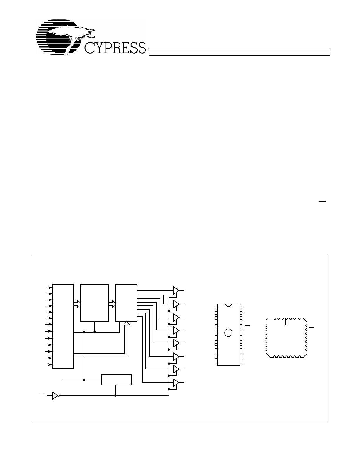
Functional Description
The CY7C261, CY7C263, and CY7C264 are high-performance 8192-word by 8-bi t CMOS PROM s. When desele cted,
the CY7C261 automatically powers down into a low-power
standby mode. It is packaged in a 300-mil-wide package. The
CY7C263 and CY7C264 are packaged in 300-mil-wide and
600-mil-wi de packages respec tively, and do not power d own
when deselected. The reprogrammable packages are
equipped with an erasure window; when exposed to UV light,
these PROMs are erased and can then be reprogrammed.
The memory cells utilize proven EPROM floating-gate
technology and byte-wid e inte lligen t p rogrammin g algo rith ms.
The CY7C261, CY7C263, and CY7C264 are plug-in replacements for bipolar devices and offer the advantages of lower
power, superior performance and programming yield. The
EPROM cell requires only 12.5V for the supervol tag e and low
current requirements allow for gang programming. The
EPROM cells allow for each memory location to be tested
100%, as each location is wri tten into , erase d, and rep eatedl y
exercised prior to encapsulation. Each PROM is also tested
for AC performance to guarantee that after customer
programming the product will meet DC and AC specification
limits.
Read is accomplish ed by placing an active LO W signal on CS
The contents of the memory location addressed by the
address line (A
).
(O
0−O7
) will become avail able on the output line s
0−A12
.
Logic Block Diagram Pin Configurations
A
0
A
1
A
2
A
3
A
4
A
5
A
6
A
7
A
8
A
9
A
10
A
11
A
12
CS
ROW
ADDRESS
ADDRESS
DECODER
COLUMN
ADDRESS
PROGRAM-
MABLE
ARRAY
COLUMN
MULTI-
PLEXER
POWER DOWN
(7C261)
For an 8K x 8 Registered PROM, see theCY7C265.
O
7
O
6
O
5
O
4
O
3
O
2
O
1
O
0
DIP/Flatpack
A
7
A
6
A
5
A
4
A
3
A
2
A
1
A
0
O
0
O
1
O
2
GND
Top View
1
2
3
4
5
6
7
7C261
8
7C263
9
7C264
10
11 14
12 13
V
24
CC
A
8
23
A
22
9
A
10
21
CS
20
A
11
19
A
12
18
O
17
7
O
6
16
O
15
5
O
4
O
3
LCC/PLCC (Opaque Only)
Top View
5
7
9
CC
NC
V
A
A6A
A8A
28
321 27
NC
4
A
5
4
A
6
3
A
2
7
A
1
8
A
9
0
10
O
0
11
1314151617
12
1
2
O
O
7C261
7C263
GND
NC
26
25
24
23
22
21
20
19
18
5
3
O4O
O
A
CS
A
A
NC
O
O
10
11
12
7
6
Cypress Semiconductor Corporation • 3901 North First Street • San Jose • CA 95134 • 408-943-2600
Document #: 38-04010 Rev. *B Revised December 28, 2002
CY7C261
CY7C263/CY7C264
Selection Guide
7C261-20
7C263-20
7C264-20
Maximum Acces s Time 20 25 35 45 55 ns
Maximum Operat ing
Current
Maximum Standby
Current (7C261 only)
Commercial 120 120 100 100 100 mA
Military 140 120 120 120 mA
Commercial 40 40 30 30 30 mA
Military 40 30 30 30 mA
7C261-25
7C263-25
7C264-25
7C261-35
7C263-35
7C264-35
7C261-45
7C263-45
7C264-45
7C261-55
7C263-55
7C264-55 Unit
Maximum Ratings
[1]
(Above which the useful life may be impaired. For user guidelines, not tested.)
Storage Temperatures.................................–65°C to+150°C
Ambient Temperature with
Power Applied..............................................–55°C to+125°C
Supply Voltage to Ground Potential
(Pin 24 to Pin 12)............................................–0.5V to+7.0V
DC Voltage Applied to Outputs
in High Z State................................................–0.5V to+7.0V
DC Input Voltage...........................................–3.0V to + 7.0V
DC Program Voltage
(Pin 19 DIP, Pin 23 LCC) ..............................................13.0V
Stat ic Disc ha rge Voltage..... .................................. .....>2001V
(per MIL-STD-883, Method 3015)
Latch-Up Current.....................................................>200 mA
UV Exposure................................................7258 Wsec/cm
Operating Range
Range
Commercial 0°C to + 70°C 5V ± 10%
[2]
Military
Notes:
1. The volatge on any input or I/O pin cannot exceed the power pin during
power-up.
2. T
is the “instant on” case temperature.
A
Ambient
Temperature V
CC
–55°C to + 125°C 5V ± 10%
2
Document #: 38-04010 Rev. *B Page 2 of 14
CY7C261
CY7C263/CY7C264
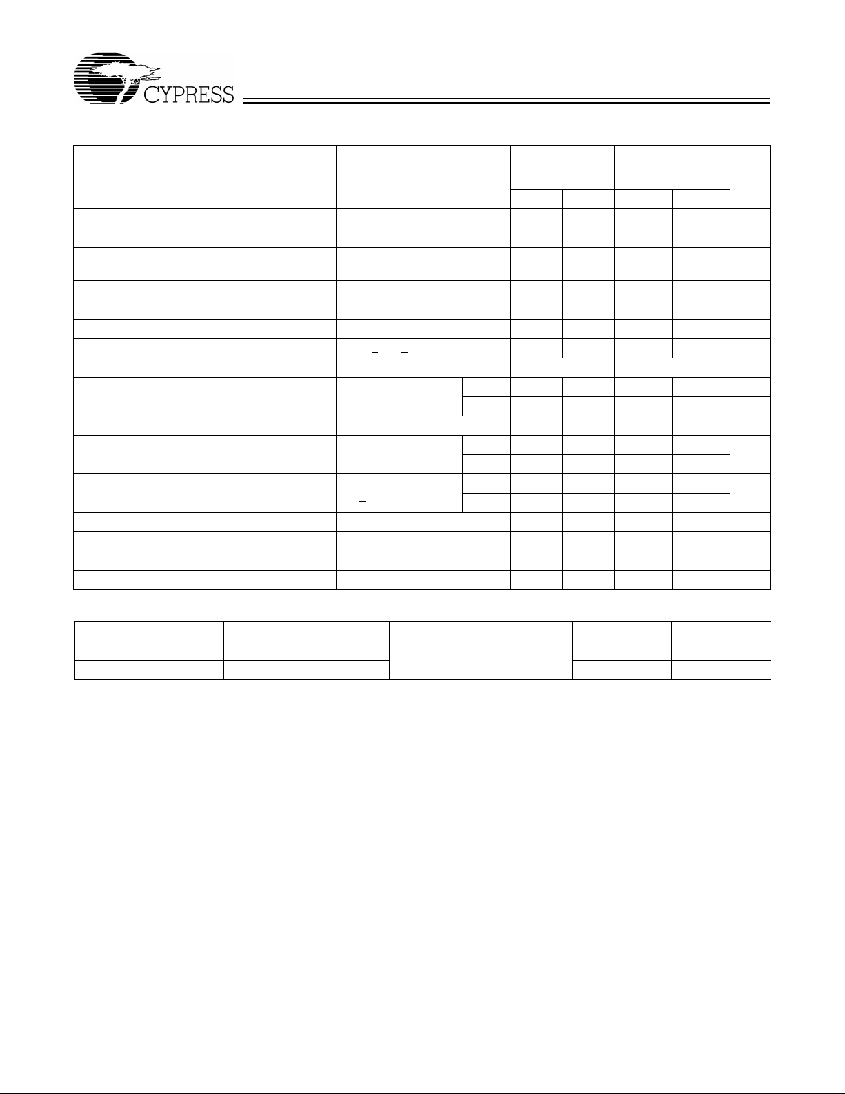
Electrical Characteristics Ov er the Op erat ing Range
[3,4]
7C261-20, 25
7C263-20, 25
7C264-20, 25
7C261-35, 45, 55
7C263-35, 45, 55
7C264-35, 45, 55
Parameter Description Test Conditions Min. Max. Min. Max. Unit
V
OH
V
OH
V
OL
V
OL
V
IH
V
IL
I
IX
V
CD
I
OZ
I
OS
I
CC
I
SB
V
PP
I
PP
V
IHP
V
ILP
Capacitance
Output HIGH Voltage VCC = Min., IOH = –2.0 mA 2.4 V
Output HIGH Voltage VCC = Min., IOH = –4.0 mA 2.4 V
Output LOW Voltage VCC = Min., IOL = 8 mA
0.4 V
(6 mA Mil)
Output LOW Voltage VCC = Min., IOL = 16 mA 0.4 V
Input HIGH Level 2.0 2.0 V
Input LOW Level 0.8 0.8 V
Input Current GND < VIN < V
CC
–10 +10 –10 +10 µA
Input Diode Clamp Voltage Note 4 Note 4
Output Leakage Current GND < V
Output Disabled
Output Short Circuit Current
[5]
VCC = Max., V
Power Supply Current VCC = Max., f = Max.
I
= 0 mA
OUT
Standby Supply Current (7C261) VCC = Max.,
> V
CS
OUT
< V
Com’l –10 +10 –10 +10 µA
CC
Mil –40 +40 –40 +40 µA
= G N D –20 –90 –20 –90 mA
OUT
Com’l 120 100 mA
Mil 140 120
Com’l 40 30 mA
IH
Mil 40 30
Programming Supply Voltage 12 13 12 13 V
Programming Supply Current 50 50 mA
Input HIGH Programming Voltage 4.75 4.75 V
Input LOW Programming Voltage 0.4 0.4 V
[4]
Parameter Description Test Conditions Max. Unit
C
IN
C
OUT
Notes:
3. See the last page of this specification for Group A subgroup testing information.
4. See the “Introduction to CMOS PROMs” section of the Cypress Data Book for general information on testing.
5. For test purposes, not more than one output at a time should be shorted. Short circuit test duration should not exceed 30 seconds.]
Input Capacitance TA = 25°C, f = 1 MHz,
= 5.0V
V
Output Capacitance 10 pF
CC
10 pF
Document #: 38-04010 Rev. *B Page 3 of 14

CY7C261
CY7C263/CY7C264
AC Test Loads and Waveforms
Test Load for -20 through -30 speeds
R1500
(658Ω
R1250Ω
MIL)
OUTPUT
R2333Ω
(403Ω
MIL)
200Ω (250Ω MIL)
R
TH
R2167Ω R2167Ω
2.0V(1.9VMIL)
OUTPUT
5V
OUTPUT
30 pF
INCLUDING
JIG AND
SCOPE
(a) Normal Load (b) HighZ Load
Equivalent to: THÉ VENIN EQUIV ALENT
OUTPUT
Test Load for -35 through -55 speeds
5V
OUTPUT
30pF
INCLUDING
JIG AND
SCOPE
[4]
5V
5pF
INCLUDING
JIG AND
SCOPE
5V
5pF
INCLUDING
JIG AND
SCOPE
R1500Ω
(658ΩMIL)
R1250Ω
R2333Ω
(403ΩMIL)
3.0V
GND
≤ 5ns
90%
10%
90%
10%
≤ 5 ns
(c)Normal Load (d) HighZ Load
Equivalent to: THÉ VENINEQUIVALENT
R
100Ω
OUTPUT 2.0V
Switching Characteristics Over the Oper ating Ra nge
TH
[1,3,4
7C261-20
7C263-20
7C264-20
]
7C261-25
7C263-25
7C264-25
7C261-35
7C263-35
7C264-35
7C261-45
7C263-45
7C264-45
7C261-55
7C263-55
7C264-55
Parameter Description Min. Max. Min. Max. Min. Max. Min. Max. Min. Max. Unit
t
AA
t
HZCS1
t
HZCS2
t
ACS1
t
ACS2
t
PU
t
PD
Address to Output Valid 20 25 35 45 55 ns
Chip Select Inactive to High Z
12 12 20 30 35 ns
(7C263 and 7C264)
Chip Select Inactive to High Z
20 25 35 45 55 ns
(7C261)
Chip Select Active to Output Valid
12 12 20 30 35 ns
(7C263 and 7C264)
Chip Select Active to Output Valid
20 25 35 45 55 ns
(7C261)
Chip Select Active to Power-Up
00000ns
(7C261)
Chip Select Inactive to
20 25 35 45 55 ns
Power-Down (7C261)
Document #: 38-04010 Rev. *B Page 4 of 14
CY7C261
CY7C263/CY7C264
Switching Wavefo rms
V
CC
SUPPLY
CURRENT
A
-A
0
12
ADDRESS
CS
O0-O
7
[4]
t
PD
t
AA
t
HZCS
Erasure Characteristics
Wavelen gths of light les s than 4000 ang stroms begin t o erase
the devices in the windowed package. For this reason, an
opaque label should be placed over the window if the PROM
is exposed to sunlight or fluorescent lighting for extended
periods of time.
The recommended dose of ultraviolet light for erasure is a
wavelength of 2537 angstroms for a minimum dose (UV
intensity multiplied by exposure time) of 25 Wsec/cm
ultraviolet lamp with a 12 mW/cm
2
power rating, the exposure ti me
would be approximately 35 minutes. The 7C261 or 7C263
needs to be within 1 inch of the lamp during erasure.
Permanent damage may result if the PROM is exposed to
high-intensity UV light for an extended period of time. 7258
Wsec/cm
2
is the recommended maximum dosage.
2
. For an
t
PU
50% 50%
t
ACS
Operating Modes
Read
Read is the normal operatin g mode for programmed device. In
this mode, all signals are normal TTL levels. The PROM is
addressed with a 13-bit field, a chip select, (active LOW), is
applied to the CS
appear on the data out pins.
Program, Program Inhibit, Program Verify
These modes are en tered b y pla cing a high volt age V
19, with pins 18 and 20 set t o V
latch signal, allowing the upp er 5 addr ess bits to b e latc hed into an
onboard register, pin 22 becomes an act ive LOW pro gram (PGM
signal and pin 23 becomes an active LOW verify (VFY
22 and 23 should ne ver be active LOW at the same time. The
PROGRAM mode exists when PGM
verify mode exists when the reverse is true, PGM
LOW and the program inhibit mode is entere d with both P GM an d
HIGH. Program inhibit is specifically provided to allow data to be
VFY
placed on and removed from the data pins without conflict
pin, and the con tents of the addressed location
on pin
. In this state, pin 21 becomes a
ILP
PP
) signal. Pins
is LOW, and VFY is HIGH. The
HIGH and VFY
)
Table 1. Mode Selection
[6, 7]
A
9
A
9
A
9
V
ILP
V
IHP
V
IHP
V
IHP
A
8
A
8
A
8
V
IHP
V
IHP
V
ILP
V
ILP
CS O7–O
V
IL
V
IH
V
ILP
V
ILP
V
ILP
V
ILP
O7–O
High Z
D7–D
High Z
O7–O
O7–O
0
0
0
0
0
0
Read or Output Disable A
12
Mode Program NA V
Read A
Output Disable A
Program V
Program Inhibit V
Program Verify V
Blank Check V
Notes:
6. X = “don’t care” but not to exceed V
7. Addresses A
must be latched through lines A0-A4 in programming modes .
8-A12
CC
12
12
ILP
ILP
ILP
ILP
±5%.
Pin Function
A
11
PP
A
11
A
11
V
PP
V
PP
V
PP
V
PP
A
10
LATCH PGM VFY CS D7–D
A
10
A
10
V
ILP
V
ILP
V
ILP
V
ILP
Document #: 38-04010 Rev. *B Page 5 of 14

CY7C261
CY7C263/CY7C264
DIP/Flatpack
Top View
24
23
22
21
20
19
18
17
16
15
V
CC
VFY
PGM
LATCH
CS
V
PP
NA
D
7
D
6
D
5
D
4
D
3
Figure 1. Programming Pinouts
A
A2/A
A4/A
3/A11
A1/A
A0/A
GND
A
7
A
6
A
5
12
10
9
8
D
0
D
1
D
2
1
2
3
4
5
6
7
8
7C261
9
7C263
7C264
10
11 14
12 13
Programming Information
Programming support is available from Cypress as well as
from a number of third-party software vendors. For detailed
programming information, including a listing of software
LCC/PLCC
(Opaque only)
Top View
5
7
CC
A6A
2
NC
7C261
7C263
NC
GND
28
V
PGM
VFY
26
LATCH
25
CS
24
V
PP
23
NA
22
21
NC
D
7
20
D
19
6
5
D
3
18
D4D
A
321 27
4
A4/A
12
2/A10
A1/A
A
0/A8
11
NC
D
5
6
7
9
8
9
10
0
11
13 14 15 16 17
12
1
D
D
A3/A
A
packages, please see the PROM Programming Information
located at the end of this s ection. Program ming algorithms can
be obtained from any Cypress representative.
Document #: 38-04010 Rev. *B Page 6 of 14

Typical DC and AC Characteristics
CY7C261
CY7C263/CY7C264
NORMALIZED SUPPLY CURRENT
vs. SUPPLY VOLTAGE
1.6
1.4
CC
1.2
1.0
NORMALIZED I
T
= 25°C
0.8
A
f= f
MAX
0.6
4.0 4.5 5.0 5.5 6.0
SUPPLY VOLTAGE (V)
NORMALIZED ACCESS TIME
vs.
TEMPERATURE
1.6
1.4
1.2
1.0
0.8
NORMALIZED ACCESS TIME
0.6
–55 125
25
AMBIENT TEMPERA T U RE (°C)
NORMALIZED SUPPLY CURRENT
vs. AMBIENT TEMPERATURE
1.2
CC
1.1
1.0
0.9
NORMALIZED I
0.8
–55 25 125
AMBIENT TEMPERATURE (°C)
OUTPUT SOURCE CURRENT
vs. V OLTAGE
60
50
40
30
20
10
0
OUTPUT SOURCE CURRENT (mA)
01.0 2.03.0
OUTPUT VOLTAGE (V)
4.0
NORMALIZED ACCESS TIME
vs.SUPPLY VOLTAGE
1.2
TIME
1.0
0.8
0.6
= 25°C
T
A
0.4
NORMALIZED ACCESS
4.0 4.5 5.0 5.5 6.0
SUPPLY VOLTAGE (V)
TYPICAL ACCESS TIME CHANGE
vs. OUT PUT
LOADING
35
30
25
20
AA
15
DELTA t (ns)
10
5
0
0 200 400 600 800
V
CC
T
A
= 4.5V
= 25°C
CAPACITANCE (pF)
1000
OUTPUT SINK CURRENT
vs. OUTPUT VOLTAGE
175
150
125
100
75
50
25
OUTPUT SINK CURRENT (mA)
0
0.0 1.0 2.0 3.0
OUTPUT VOLTAGE (V)
VCC= 5.0V
= 25°C
T
A
4.0
NORMALIZED SUPPLY CURRENT
vs. CYCLE PERIOD
1.05
1.00
CC
0.95
0.90
0.85
0.80
NORMALIZED I
0.75
0.70
025 5075
CYCLE PERIOD (ns)
VCC= 5.5V
T
= 25°C
A
100
Document #: 38-04010 Rev. *B Page 7 of 14

CY7C261
CY7C263/CY7C264
]
Ordering Information
Speed
(ns) Ordering Code
20 CY7C261-20PC P13 24-Lead (300-Mil) Molded DIP Commercial
CY7C261-20WC W14 24-Lead (300-Mil) Windowed CerDIP
25 CY7C261-25JC J64 28-Lead Plastic Leaded Chip Carrier Commercial
CY7C261-25PC P13 24-Lead (300-Mil) Molded DIP
CY7C261-25WMB W14 24-Lead (300-Mil) Windowed CerDIP Military
35 CY7C261-35PC P13 24-Lead (300-Mil) Molded DIP Commercial
CY7C261-35WC W14 24-Lead (300-Mil) Windowed CerDIP
CY7C261-35WMB W14 24-Lead (300-Mil) Windowed CerDIP Military
45 CY7C261-45PC P13 224-Lead (300-Mil) Molded DIP Commercial
CY7C261-45WC W14 24-Lead (300-Mil) Windowed CerDIP
CY7C261-45WMB W14 24-Lead (300-Mil) Windowed CerDIP Military
55 CY7C261-55WC W14 24-Lead (300-Mil) Windowed CerDIP Commercial
20 CY7C263-20JC J64 28-Lead Plastic Leaded Chip Carrier Commercial
CY7C263-20PC P13 24-Lead (300-Mil) Molded DIP
CY7C263-20WC W14 24-Lead (300-Mil) Windowed CerDIP
25 CY7C263-25JC J64 28-Lead Plastic Leaded Chip Carrier Commercial
CY7C263-25PC P13 24-Lead (300-Mil) Molded DIP
CY7C263-25WC W14 24-Lead (300-Mil) Windowed CerDIP
CY7C263-25DMB D14 24-Lead (300-Mil) CerDIP Military
CY7C263-25QMB Q64 28-Pin Win dowe d Lead les s Chip Carri er
CY7C263-25WMB W14 24-Lead (300-Mil) Windowed CerDIP
35 CY7C263-35PC P13 24-Lead (300-Mil) Molded DIP Commercial
CY7C263-35WC W14 24-Lead (300-Mil) Windowed CerDIP
CY7C263-35WMB W14 24-Lead (300-Mil) Windowed CerDIP Military
45 CY7C263-45WMB W14 24-Lead (300-Mil) Windowed CerDIP Military
55 CY7C263-55JI J64 28-Lead Plastic Leaded Chip Carrier Industrial
CY7C263-55PC P13 24-Lead (300-Mil) Molded DIP Commercial
CY7C263-55WMB W14 24-Lead (300-Mil) Windowed CerDIP Military
35 CY7C264-35PC P11 24-Lead (600-Mil) Molded DIP Commercial
45 CY7C264-45WC W12 24-Lead (600-Mil) Windowed CerDIP Commercial
CY7C264-45WMB W12 24-Lead (600-Mil) Windowed CerDIP Military
55 CY7C264-55WC W12 24-Lead (600-Mil) Windowed CerDIP Commercial
Package
Name Package Type
Operating
Range
Document #: 38-04010 Rev. *B Page 8 of 14

MILITARY SPECIFICATION
Group A Subgroup Testing
CY7C261
CY7C263/CY7C264
DC Characteristics
Parameter Subgroups
V
OH
V
OL
V
IH
V
IL
I
IX
I
OZ
I
CC
[8]
I
SB
1, 2, 3
1, 2, 3
1, 2, 3
1, 2, 3
1, 2, 3
1, 2, 3
1, 2, 3
1, 2, 3
Switching Characteristics
Parameter Subgroups
t
AA
[9]
t
ACS1
[8]
t
ACS2
Notes:
8. 7C261 only.
9. 7C263 and 7C264 only.
7, 8, 9, 10, 11
7, 8, 9, 10, 11
7, 8, 9, 10, 11
Document #: 38-04010 Rev. *B Page 9 of 14

Package Diagrams
CY7C261
CY7C263/CY7C264
24-Lead (300-Mil) CerDIP D14
MIL-STD-1835 D- 9 Config.A
28-Lead Plastic Leaded Chip Carrier J64
51-80031
51-85001-A
Document #: 38-04010 Rev. *B Page 10 of 14

Package Diagrams (continued)
CY7C261
CY7C263/CY7C264
24-Lead (600-Mil) Molded DIP P11
51-85016-A
24-Lead (300-Mil) Molded DIP P13/P13A
51-85013-A
Document #: 38-04010 Rev. *B P age 11 of 14

Package Diagrams (continued)
CY7C261
CY7C263/CY7C264
28-PinWindowedLeadless Chip Carrier Q64
MIL–STD–1835 C–4
51-80102
Document #: 38-04010 Rev. *B Page 12 of 14

Package Diagrams (continued)
CY7C261
CY7C263/CY7C264
24-Lead (600-Mil) Windowed CerDIP W12
MIL-STD-1835 D-3 Config. A
51-80089-**
24-Lead (300-Mil) Windowed CerDIP W14
MIL-STD-1835 D-9 Config. A
51-80086
All product and company names mentioned in this document may be the trademarks of their respective holders.
Document #: 38-04010 Rev. *B Page 13 of 14
© Cypress Semiconductor Corporation, 2002. The information contained herein is subject to change without notice. Cypress Semiconductor Corporation assumes no responsibility for the use
of any circuitry other than cir cuitry embodi ed in a Cypress S emiconductor product . Nor does it convey or imply any license un der patent or other righ ts. Cypre ss Semiconductor does not autho rize
its products for use as critical components in life-support systems where a malfunction or failure may reasonably be expected to result in significant injury to the user. The inclusion of Cypress
Semiconductor products in life-support systems application implies that the manufacturer assumes all risk of such use and in doing so indemnifies Cypress Semiconductor against all charges.

CY7C263/CY7C264
Document History Page
Document Title: CY7C261 CY7C263/CY7C264 8K x 8 Power Switched and Reprogrammable PROM
Document Number: 38-04010
REV. ECN NO.
** 113866 3/6/02 DSG Change from Spec number: 38-00005 to 38-04010
*A 1 1 889 5 10/09/02 GBI Update Ordering Information
*B 122251 12/28/02 RBI Add power up requirements to Maximum Ratings information
)
Issue
Date
Orig. of
Change Description of Change
CY7C261
Document #: 38-04010 Rev. *B Page 14 of 14
 Loading...