

Cypress Semiconductor CY7C1382CV25-167AI, CY7C1382CV25-167AC, CY7C1380CV25-250BZC, CY7C1380CV25-250BGC, CY7C1380CV25-250AC Datasheet
...
512K x 36/1M x 18 Pipelined SRAM
CY7C1380CV25
CY7C1382CV25
PRELIMINARY
Cypress Semiconductor Corporation • 3901 North First Street • San Jose, CA 95134 • 408-943-2600
Document #: 38-05240 Rev. *A Revised November 20, 2002
380CV25
Features
• Fast clock speed: 250, 225, 200, 167 MHz
• Provide high-performance 3-1-1-1 access rate
•Fast OE
access times: 2.6, 2.8, 3.0, 3.4 ns
• Optimal for depth expansion
• Single 2.5V ±5% power supply
• Common data inputs and data outputs
• Byte Write Enable and Global Write control
• Chip enable for address pipeline
• Address, data, and control registers
• Internally self-timed Write cycle
• Burst control pins (interleaved or linear burst
sequence)
• Automatic power-down available using ZZ mode or CE
deselect
• Available in 119-ball bump BGA, 165-ball FBGA and
100-pin TQFP packages
• JTAG boundary scan for BGA packaging version
Functional Description
The Cypress Synchronous Burst SRAM family employs highspeed, low-power CM OS designs using adv anced single-lay er
polysilicon, triple-lay er metal technology. Each memory cell
consists of six transistors.
The CY7C1382CV25 and CY7C1380CV25 SRAMs integrate
1,048,576x18 and 524,288x36 SRAM cells with advanced
synchronous peripheral circuitry and a 2-bit counter for internal burst operation. All synchronous inputs are gated by registers controlled by a positive-edge-triggered clock input
(CLK). The synchrono us in put s i nc lud e a ll addresses, all dat a
inputs, address-pipelining chip enable (CE
), burst control inputs (ADSC, ADSP, and ADV), write enables (BWa, BWb,
BW
c, BWd and BWE), and global write (GW).
Asynchronous input s include the output enable (OE
) and burst
mode control (MODE). T he data (D Qa,b,c,d) and the dat a parity (DQPa,b,c,d) outputs, enabled by OE
, are also asynchro-
nous.
DQa,b,c,d and DPa,b,c,d apply to CY7C1380CV25 and
DQa,b and DPa,b apply to CY7C1382CV25. a, b, c, d each
are of 8 bits wide in the case of DQ and 1 bit wid e in the cas e
of DP.
Addresses and chip enables ar e registered with either address
status processor (ADSP
) or address status controller (ADSC)
input pins. Subsequent burs t addresses can be in ternally generated as controlled by the burst advance pin (ADV
).
Address, data inputs, and write contr ols are regis tered on-chi p
to initiate self-timed Write cycle. Write cycles can be one to
four bytes wide as controlled by the write control inputs. Individual byte write allows ind ividual byte to be writt en. BW
a con-
trols DQa and DPa. BW
b controls DQb and DPb . BWc controls
DQc and DPd. BW
d controls DQd and DPd. BWa, BWb BWc,
and BW
d can be active only with BWE bein g LOW. GW being
LOW causes all bytes to be w ri tten . Write pass-throu gh c apability allows written data available at the output for the next
Read cycle. This device also incorporates pipelined enable
circuit for easy depth expansion without penalizing system
performance.
All inputs and outputs of the CY7C1380CV25 and the
CY7C1382CV25 are JEDEC st an dar d JESD 8-5 co mpatible.
Selection Guide
250 MHz 225 MHz 200 MHz 167 MHz Unit
Maximum Acces s Time 2.6 2.8 3.0 3.4 ns
Maximum Operating Curre nt 350 325 300 275 mA
Maximum CMOS Standby Current 70 70 70 70 mA
Shaded areas contain advance information.

CY7C1380CV25
CY7C1382CV25
PRELIMINARY
Document #: 38-05240 Rev. *A Page 2 of 33
CLK
ADV
ADSC
A
[18:0]
GW
BWE
BW
d
BW
c
BW
b
BW
a
CE
1
CE
3
CE
2
OE
ZZ
BURST
COUNTER
ADDRESS
REGISTER
OUTPUT
REGISTERS
INPUT
REGISTERS
512KX36
MEMORY
ARRAY
CLK
CLK
Q
0
Q
1
Q
D
CE
CE
CLR
SLEEP
CONTROL
36 36
19
17
17
19
(A
[1;0]
)
2
MODE
ADSP
DQ
a,b,c,d
DP
a,b
DQd, DPd
BYTEWRITE
REGISTERS
DQ
DQc, DPc
BYTEWRITE
REGISTERS
DQ
DQ
DQb, DPb
BYTEWRITE
REGISTERS
DQa, DPa
BYTEWRITE
REGISTERS
DQ
ENABLE CE
REGISTER
DQ
ENABLE DELAY
REGISTER
DQ
CY7C1380CV25 - 512K x 36
CLK
ADV
ADSC
A
[19:0]
GW
BWE
BW
b
BW
a
CE
1
CE
3
CE
2
OE
ZZ
BURST
COUNTER
ADDRESS
REGISTER
OUTPUT
REGISTERS
INPUT
REGISTERS
MEMORY
ARRAY
CLK
CLK
Q
0
Q
1
Q
D
CE
CE
CLR
SLEEP
CONTROL
18 18
20
18
18
20
(A
[1;0]
)
2
MODE
ADSP
CY7C1382CV25 - 1M X 18
DQ
a,b
DP
a,b
DQb, DPb
BYTEWRITE
REGISTERS
DQ
DQa, DPa
BYTEWRITE
REGISTERS
DQ
ENABLE CE
REGISTER
DQ
ENABLE DELAY
REGISTER
DQ
CE
1M X 18

CY7C1380CV25
CY7C1382CV25
PRELIMINARY
Document #: 38-05240 Rev. *A Page 3 of 33
Pin Configurations
AAA
A
A
1A0
NC
NC
V
SS
V
DD
A
AAAAA
A
A
A
NC
NC
V
DDQ
V
SSQ
NC
DPa
DQa
DQa
V
SSQ
V
DDQ
DQa
DQa
V
SS
NC
V
DD
ZZ
DQa
DQa
V
DDQ
V
SSQ
DQa
DQa
NC
NC
V
SSQ
V
DDQ
NC
NC
NC
NC
NC
NC
V
DDQ
V
SSQ
NC
NC
DQb
DQb
V
SSQ
V
DDQ
DQb
DQb
V
DD
NC
V
SS
DQb
DQb
V
DDQ
V
SSQ
DQb
DQb
DPb
NC
V
SSQ
V
DDQ
NC
NC
NC
A
A
CE
1CE2
NCNCBWb
BWa
CE3VDDV
SS
CLKGWBWEOEADSC
ADSP
ADV
A
A
1
2
3
4
5
6
7
8
9
10
11
12
13
14
15
16
17
18
19
20
21
22
23
24
25
26
27
28
29
30
31323334353637383940414243444546474849
50
80
79
78
77
76
75
74
73
72
71
70
69
68
67
66
65
64
63
62
61
60
59
58
57
56
55
54
53
52
51
100999897969594939291908988878685848382
81
MODE
CY7C1382CV25
(1M x 18)
NC
AAA
A
A
1A0
NC
NC
V
SS
V
DD
A
A
AAAAA
A
A
NC,DQPb
DQb
DQb
V
DDQ
V
SSQ
DQb
DQb
DQb
DQb
V
SSQ
V
DDQ
DQb
DQb
V
SS
NC
V
DD
ZZ
DQa
DQa
V
DDQ
V
SSQ
DQa
DQa
DQa
DQa
V
SSQ
V
DDQ
DQa
DQa
NC,DQPa
NC,DQPc
DQc
DQc
V
DDQ
V
SSQ
DQc
DQc
DQc
DQc
V
SSQ
V
DDQ
DQc
DQc
V
DD
NC
V
SS
DQd
DQd
V
DDQ
V
SSQ
DQd
DQd
DQd
DQd
V
SSQ
V
DDQ
DQd
DQd
NC,DQPd
AACE1CE2BWd
BWc
BWb
BWa
CE3VDDV
SS
CLKGWBWEOEADSC
ADSP
ADV
A
A
1
2
3
4
5
6
7
8
9
10
11
12
13
14
15
16
17
18
19
20
21
22
23
24
25
26
27
28
29
30
31323334353637383940414243444546474849
50
80
79
78
77
76
75
74
73
72
71
70
69
68
67
66
65
64
63
62
61
60
59
58
57
56
55
54
53
52
51
100999897969594939291908988878685848382
81
MODE
CY7C1380CV25
(512K X 36)
NC
A
100-Pin TQFP
Top View

CY7C1380CV25
CY7C1382CV25
PRELIMINARY
Document #: 38-05240 Rev. *A Page 4 of 33
119-Ball BGA
Pin Configurations (continued)
2
3
4
5
6
7
1
A
B
C
D
E
F
G
H
J
K
L
M
N
P
R
T
U
V
DDQ
NC
NC
DQPc
DQc
DQd
DQc
DQd
A
A
A
A
ADSP
V
DDQ
A
DQc
V
DDQ
DQc
V
DDQ
V
DDQ
V
DDQ
DQd
DQd
NC
NC
V
DDQ
V
DD
CLK
V
DD
V
SS
V
SS
V
SS
V
SS
V
SS
V
SS
V
SS
V
SS
NC
NC
NC
NC
TDO
TCK
TDITMS
36M
72M
NC
V
DDQ
V
DDQ
V
DDQ
A
A
A
A
A
A
A
A
A
A
A
A0
A1
DQa
DQc
DQa
DQa
DQa
DQb
DQb
DQb
DQb
DQb
DQb
DQb
DQa
DQa
DQa
DQa
DQb
V
DD
DQc
DQc
DQc
V
DD
DQd
DQd
DQd
DQd
ADSC
NC
CE
1
OE
ADV
GW
V
SS
V
SS
V
SS
V
SS
V
SS
V
SS
V
SS
V
SS
DQPa
MODE
DQPd
DQPb
BWb
BWc
NC
V
DD
NC
BWa
NC
BWE
BWd
ZZ
2
3
4
5
6
7
1
A
B
C
D
E
F
G
H
J
K
L
M
N
P
R
T
U
V
DDQ
NC
NC
NCDQb
DQb
DQb
DQb
A
A
A
A
ADSP
V
DDQ
A
NC
V
DDQ
NC
V
DDQ
V
DDQ
V
DDQ
NC
NC
NC
72M
V
DDQ
V
DD
CLK
V
DD
V
SS
V
SS
V
SS
V
SS
V
SS
V
SS
V
SS
V
SS
NC
NC
NC
NC
TDOTCK
TDITMS
A
A
NC
V
DDQ
V
DDQ
V
DDQ
A
36M A
A
A
A
A
A
A
A
A
A0
A1
DQa
DQb
NC
NC
DQa
NC
DQa
DQa
NC
NC
DQa
NC
DQa
NC
DQa
NC
DQa
V
DD
NC
DQb
NC
V
DD
DQb
NC
DQb
NC
ADSC
NC
CE
1
OE
ADV
GW
V
SS
V
SS
V
SS
V
SS
V
SS
V
SS
V
SS
V
SS
NC
MODE
DQPb
DQPa
V
SS
BWb
NC
V
DD
NC
BW
a
NC
BWE
V
SS
ZZ
CY7C1382CV25 (1 M x 1 8)
CY7C1380CV25 (512K x 36)
A
A

CY7C1380CV25
CY7C1382CV25
PRELIMINARY
Document #: 38-05240 Rev. *A Page 5 of 33
Pin Configurations (continued)
CY7C1380CV25 (512K x 36) - 11 x 15 FBGA
165-Ball Bump FBGA
CY7C1382CV25 (1M x 18) - 11 x 15 FBGA
2345671
A
B
C
D
E
F
G
H
J
K
L
M
N
P
R
TDO
NC
NC
NC
NC
DPb
NC
DQb
ACE
1
NC CE
3
BWbBWE
ACE
2
NC
DQb
DQb
MODE
NC
DQb
DQb
NC
NC
NC
36M
72M
V
DDQ
NC BWaCLKGW
V
SS
V
SS
V
SS
V
SS
V
DDQ
V
SS
V
DD
V
SS
V
SS
V
SS
A
V
SS
V
SS
V
SS
V
SS
V
DDQ
V
DDQ
NC
V
DDQ
V
DDQ
V
DDQ
V
DDQ
A
A
V
DD
V
SS
V
DD
V
SS
V
SS
V
DDQ
V
DD
V
SS
V
DD
V
SS
V
DD
V
SS
V
SS
V
SS
V
DD
V
DD
V
SS
V
DD
V
SS
V
SS
NC
TCKA0
V
SS
ATDI
ATMS
DQb V
SS
NC V
SS
DQb
NC
V
SS
V
SS
V
SS
V
SS
V
SS
V
SS
V
SS
A1
DQb
NC
NC
NC
V
DDQ
V
SS
891011
A
ADV
AADSC A
OE
ADSP A 144M
V
SS
V
DDQ
NC DPa
V
DDQ
V
DD
NC
DQa
DQa
NC
NC
NC
DQa
NC
V
DD
V
DDQ
V
DD
V
DDQ
DQa
V
DD
NC
V
DD
NCV
DD
V
DDQ
DQa
V
DDQ
V
DD
V
DD
V
DDQ
V
DD
V
DDQ
NC
V
DDQ
AA
V
SS
AA
AA
DQa
NC
NC
ZZ
DQa
NC
NC
DQa
A
V
DDQ
2345671
A
B
C
D
E
F
G
H
J
K
L
M
N
P
R
TDO
NC
NC
DPc
DQc
DPd
NC
DQd
ACE
1
BWbCE
3
BWcBWE
ACE
2
DQc
DQd
DQd
MODE
NC
DQc
DQc
DQd
DQd
DQd
36M
72M
V
DDQ
BWdBWaCLK GW
V
SS
V
SS
V
SS
V
SS
V
DDQ
V
SS
V
DD
V
SS
V
SS
V
SS
A
V
SS
V
SS
V
SS
V
SS
V
DDQ
V
DDQ
NC
V
DDQ
V
DDQ
V
DDQ
V
DDQ
A
A
V
DD
V
SS
V
DD
V
SS
V
SS
V
DDQ
V
DD
V
SS
V
DD
V
SS
V
DD
V
SS
V
SS
V
SS
V
DD
V
DD
V
SS
V
DD
V
SS
V
SS
NC
TCKA0
V
SS
ATDI
ATMS
DQc V
SS
DQc V
SS
DQc
DQc
V
SS
V
SS
V
SS
V
SS
V
SS
V
SS
V
SS
A1
DQd
DQd
NC
NC
V
DDQ
V
SS
891011
A
ADV
AADSC NC
OE
ADSP A144M
V
SS
V
DDQ
NC DPb
V
DDQ
V
DD
DQb
DQb
DQb
NC
DQb
NC
DQa
DQa
V
DD
V
DDQ
V
DD
V
DDQ
DQb
V
DD
NC
V
DD
DQaV
DD
V
DDQ
DQa
V
DDQ
V
DD
V
DD
V
DDQ
V
DD
V
DDQ
DQa
V
DDQ
AA
V
SS
AA
AA
DQb
DQb
DQb
ZZ
DQa
DQa
DPa
DQa
A
V
DDQ
CY7C1380CV25
CY7C1382CV25
PRELIMINARY
Document #: 38-05240 Rev. *A Page 6 of 33
Pin Definitions
Name I/O Description
A0
A1
A
Input-
Synchronous
Address Inputs use d to s elec t one of the addre ss lo cations. Sampled at
the rising edge of the CLK if ADSP
or ADSC is active LOW, and CE1, CE2,
and
CE3
are sampled active. A
[1:0]
feed the 2-bit counter .
BWa
BWb
BWc
BWd
Input-
Synchronous
Byte Write Select Inputs, active LOW. Qualified with BWE to conduct byte
writes to the SRAM. Sampled on the rising edge of CLK.
GW Input-
Synchronous
Global Write Enable Inpu t, ac tive LOW. When asserted LOW on the rising
edge of CLK, a globa l write is cond ucted (ALL byte s are written, regardless of
the values on BW
a,b,c,d and BWE).
BWE Input-
Synchronous
Byte Write Enable Input, active LOW. Sampled on the rising edge of CLK.
This signal must be asserted LOW to conduct a byte write.
CLK Input-Clock Clock Input. Used to capture all sy nchronou s input s to the devi ce. Also used
to increment the burst counter when ADV
is asserted LOW, during a burst
operation.
CE
1
Input-
Synchronous
Chip Enable 1 Input, active LOW. Sampled on the rising edge of CLK. Used
in conjunction with CE
2
and CE3 to select/deselect the device. ADSP is ig-
nored if CE
1
is HIGH.
CE
2
Input-
Synchronous
Chip Enable 2 Input, active HIGH. Sampled on the rising edge of CL K. Used
in conjunction with CE
1
and CE3 to select/deselect the device. (TQFP Only)
CE
3
Input-
Synchronous
Chip Enable 3 Input, active LOW. Sampled on the rising edge of CLK. Used
in conjunction with CE
1
and CE2 to select/deselect the device. (TQFP Only)
OE Input-
Asynchronous
Output Enable, asynchronous inp ut, active LOW . Contr ols the directi on of
the I/O pins. When LOW, the I/O pins behave as outputs. When deasserted
HIGH, I/O pins are three-stated, and act as input data pins. OE
is masked
during the first clock of a read cycle when emerging from a deselected state.
ADV Input-
Synchronous
Advance Input signal, sa mpled on the rising edge of CLK. When asserted,
it automatically increments the address in a burst cycle.
ADSP Input-
Synchronous
Address Strobe from Processor, sampled on the rising edge of CLK.
When asserted LOW, A is captured in the address registers. A
[1:0]
are also
loaded into the burs t counter . Wh en ADSP
and ADSC are both asserted, only
ADSP
is recognized. ASDP is ignored when CE1 is deasserted HIGH.
ADSC Input-
Synchronous
Address Strobe from Controller, sampled on the rising edge of CLK.
When asserted LOW , A
[x:0]
is captured in the a ddress registe rs. A
[1:0]
are also
loaded into the burs t counter . Wh en ADSP
and ADSC are both asserted, only
ADSP is recognized.
MODE Input-Pin Selects Burst Order . Wh en tied to GND selects lin ear burst se quence. When
tied to V
DDQ
or left floating select s interleaved burs t sequence. Thi s is a strap
pin and should remain static during device operation.
ZZ Input-
Asynchronous
ZZ “sleep” Input. This active HIGH input places the device in a non-time
critical “sleep” condition with data integrity preserved.
DQa, DPa
DQb, DPb
DQc, DPc
DQd, DPd
I/O-
Synchronous
Bidirectional Data I/O lines. As inputs, they feed into an on-chip data regi ster
that is triggered by the rising edge of CLK. As outputs, they deliver the data
contained in the memory location specified by A
[X]
during the previous clock
rise of the read cycle. The d irecti on of the p ins i s co ntrolle d by OE. W hen OE
is asserted LOW , the pins behav e as outputs. Whe n HIGH, DQx and DPx
are
placed in a three-state condition. DQ a,b,c, and d are 8 bits wide and the DP
a,b,c, and d are 1 bit wide.
TDO JTAG serial output
Synchronous
Serial data-out to the JTAG circuit. Delivers data on the negative edge of
TCK. (BGA Only)
TDI JTAG serial input
Synchronous
Serial data-in to the JT AG circuit . Sampled on the rising e dge of TCK.(BGA
Only)
CY7C1380CV25
CY7C1382CV25
PRELIMINARY
Document #: 38-05240 Rev. *A Page 7 of 33
TMS Test Mode Select
Synchronous
This pin controls the Test Access Port state machine. Sampled on the
rising edge of TCK. (BGA Only)
TCK JTAG serial clock Serial clock to the JTAG circuit. (BGA Only)
V
DD
Power Supply Power supply inputs to the core of the dev ice. Should be connected to 2.5V
± 5% power su pply.
V
SS
Ground Ground for the core of the device. Should be conne cte d to ground of the
system.
V
DDQ
I/O Power Supply Power supply for the I/O circuitry.
V
SSQ
I/O Ground Ground for the I/O circuitry. Should be connected to ground of the system.
NC - No Connects.Pins are not internally connected.
36M
72M
144M
- No Connects. Reserved for address expansion.
Pin Definitions
Name I/O Description

CY7C1380CV25
CY7C1382CV25
PRELIMINARY
Document #: 38-05240 Rev. *A Page 8 of 33
Introduction
Functional Overview
All synchronous inpu ts pas s through i nput reg isters contro lled
by the rising edge of the clock. All data outputs pass through
output registers control led by the rising edge o f the clock. Maximum access delay from the clock rise (t
CO
) is 2.6 ns (250-MHz
device).
The CY7C1380CV25/CY7C1382CV25 supports secondary
cache in systems utilizing either a linear or interleaved burst
sequence. The interlea ved burst order s upports Pentiu m
®
and
i486 processors. The linear burst sequence is suited for processors that utiliz e a lin ear burst se quenc e. The b urst ord er is
user selecta ble , an d i s d etermined by sampli ng the MO DE i nput. Accesses can be initiated with either the Processor
Address Strobe (ADSP
) or the Controller Address Strobe
(ADSC
). Address advancement th rough the burs t sequence i s
controlled by the ADV
input. A two-bit on-chip wraparound
burst counter captures the first address in a burst sequence
and automatically increments the address for the rest of the
burst access.
Byte write operations are qualified with the Byte Write Enable
(BWE
) and Byte Write Select (BW
a,b,c,d
for CY7C1380V25 and
BW
a,b
for CY7C1382V25) inputs. A Gl obal Write Enab le (GW)
overrides all byte write input s and w rites data to all four by tes.
All writes are simplified with on-chip synchronous self-timed
write circuitry.
Synchronous Chip Select s (CE
1
, CE2, CE3 for TQFP / CE1 for
BGA) and an asynchronous Output Enable (OE
) provide for
easy bank selection and output three-state control. ADSP
is
ignored if CE
1
is HIGH.
Single Read Accesses
This access is initiated when the following conditions are satisfied at clock rise: (1) ADSP
or ADSC is asserted LOW, (2)
chip selects are all asserted active, and (3) the write signals
(GW
, BWE) are all deasserted HIGH. ADSP is ignored if CE
1
is HIGH. The address presented to the address inputs is
stored into the address advancement logic and the Address
Register while being presented to the memory core. The corresponding data is allowed to propagate to the input of the
Output Registers. At the risin g edge of the ne xt cloc k the dat a
is allowed to propagate through the output register and onto
the data bus within 2.6 ns (250-MHz device) if OE
is active
LOW. The only exception occurs when the SRAM is emerging
from a deselected state to a selected state, its outputs are
always three-stated during the first cycle of the access. After
the first cycle of the access, the outputs are controlled by the
OE
signal. Consecutive single read cycles are supported.
Once the SRAM is deselected at clock rise by the chip select
and either ADSP
or ADSC signals, its output will thr ee-state
immediately.
Single Write Accesses Initiated by ADSP
This access is initiated when both of the following conditions
are satisfied at clock rise: (1) ADSP
is asserted LOW, and (2)
chip select is asserted active. The address presented is loaded into the address register and the address advancement
logic while being deli vered to the RAM c ore. The wr ite signal s
(GW
, BWE, and BWx) and ADV inputs are ignored during this
first cycle.
ADSP
triggered write accesses require two clock cycles to
complete. If GW
is asserted LOW on the second clock rise, th e
data presented to the DQx inputs is written into the corresponding address location in the RAM core. If GW
is HIGH,
then the write operation is controlled by BWE
and BWx signals. The CY7C1380CV25/CY7C1382CV25 provides byte
write capabi li ty t h at i s de sc r ibe d i n th e wr ite c ycl e de s cri pt i on
table. Asserting the Byte Write Enable input (BWE
) with the
selected Byte Write (BWa,b,c,d for CY7C1380CV25 and
BW
a,b for CY7C1382CV25) input will selectively write to only
the desired bytes. Bytes not selec ted during a byte write op eration will remain unaltered. A synchronous self-timed write
mechanism has b een provided to simpli fy the write operatio ns.
Because the CY7C1380CV25/CY7C1382CV25 is a common
I/O device, the output enable (OE
) must be deasserted HIGH
before presenting data to the DQ
inputs. Doing so will threestate the output drivers. As a safety precaution, DQ are automatically three-stated whenever a write cycle is detected, regardless of the state of OE
.
Single Write Accesses Initiated by ADSC
ADSC write accesses are initiated when the following conditions are satisfied: (1) ADSC
is asserted LOW, (2) ADSP is
deasserted HIGH, (3) chip select is asserted active, and (4)
the appropriate combination of the write inputs (GW
, BWE,
and BW
x) are asserted active to con duct a write to the des ired
byte(s). ADSC
triggered write accesses require a single clock
cycle to complete. The address presented to A
[17:0]
is loaded
into the address register and the address advancement logic
while being delivered to the RAM core. The ADV
input is ig nored during this cycle. If a g lobal write is co nduct ed, the dat a
presented to the DQ[x:0] is written into the corresponding address location in the RAM core. If a byte write is conducted,
only the selected bytes are written. Bytes not selected during
a byte write operation will remain unaltered. A synchronous
self-timed write mechanism has been provided to simplify the
write operations.
Because the CY7C1380CV25/CY7C1382CV25 is a common
I/O device, the output enable (OE
) must be deasserted HIGH
before presenting data to the DQ[x:0] inputs. Doing so will
three-state the output drivers. As a saf ety pr ecauti on, DQ[x:0]
are automatically three-stated whenever a write cycle is detected, regardless of the state of OE
.
Burst Sequences
The CY7C1380CV25/CY7C1382CV25 provides a two-bit
wraparound counter, fed by A
[1:0]
, that implements either an
interleaved or linear burst s equence. The interle aved burst sequence is designed specifically to support Intel
®
Pentium applications. The linear burst sequence is designed to support
processors that follow a linear burst sequence. The burst sequence is user selectable through the MODE input.
Asserting ADV
LOW at clock rise will automa tic al ly increment
the burst counter to the next address in the burst sequence.
Both read and write burst operations are supported.

CY7C1380CV25
CY7C1382CV25
PRELIMINARY
Document #: 38-05240 Rev. *A Page 9 of 33
Sleep Mode
The ZZ input pin is an asynchronous input. Asserting ZZ places the SRAM in a power conservation “sleep” mode. T wo clock
cycles are required to enter into or exit from this “sleep” mode.
While in this mode, data integrity is guaranteed. Accesses
pending when entering the “sleep” mode are not considered
valid nor is the completion of the operation guaranteed. The
device must be d ese lected prior to ent ering the “sleep” mode.
CE
s, ADSP, and ADSC must remain inactive for the duration
of t
ZZREC
after the ZZ input returns LOW.
Interleaved Burst Sequence
First
Address
Second
Address
Third
Address
Fourth
Address
A
[1:0]]
A
[1:0]
A
[1:0]
A
[1:0]
00 01 10 11
01 00 11 10
10 11 00 01
11 10 01 00
Linear Burst Sequence
First
Address
Second
Address
Third
Address
Fourth
Address
A
[1:0]
A
[1:0]
A
[1:0]
A
[1:0]
00 01 10 11
01 10 11 00
10 11 00 01
11 00 01 10
ZZ Mode Electrical Characteristics
Parameter Description Test Conditions Min. Max. Unit
I
DDZZ
Sleep mode stand-
by current
ZZ > VDD − 0.2V 60 mA
t
ZZS
Device operation to ZZZZ > VDD − 0.2V 2t
CYC
ns
t
ZZREC
ZZ recovery time ZZ < 0.2V 2t
CYC
ns
CY7C1380CV25
CY7C1382CV25
PRELIMINARY
Document #: 38-05240 Rev. *A Page 10 of 33
Cycle Descriptions
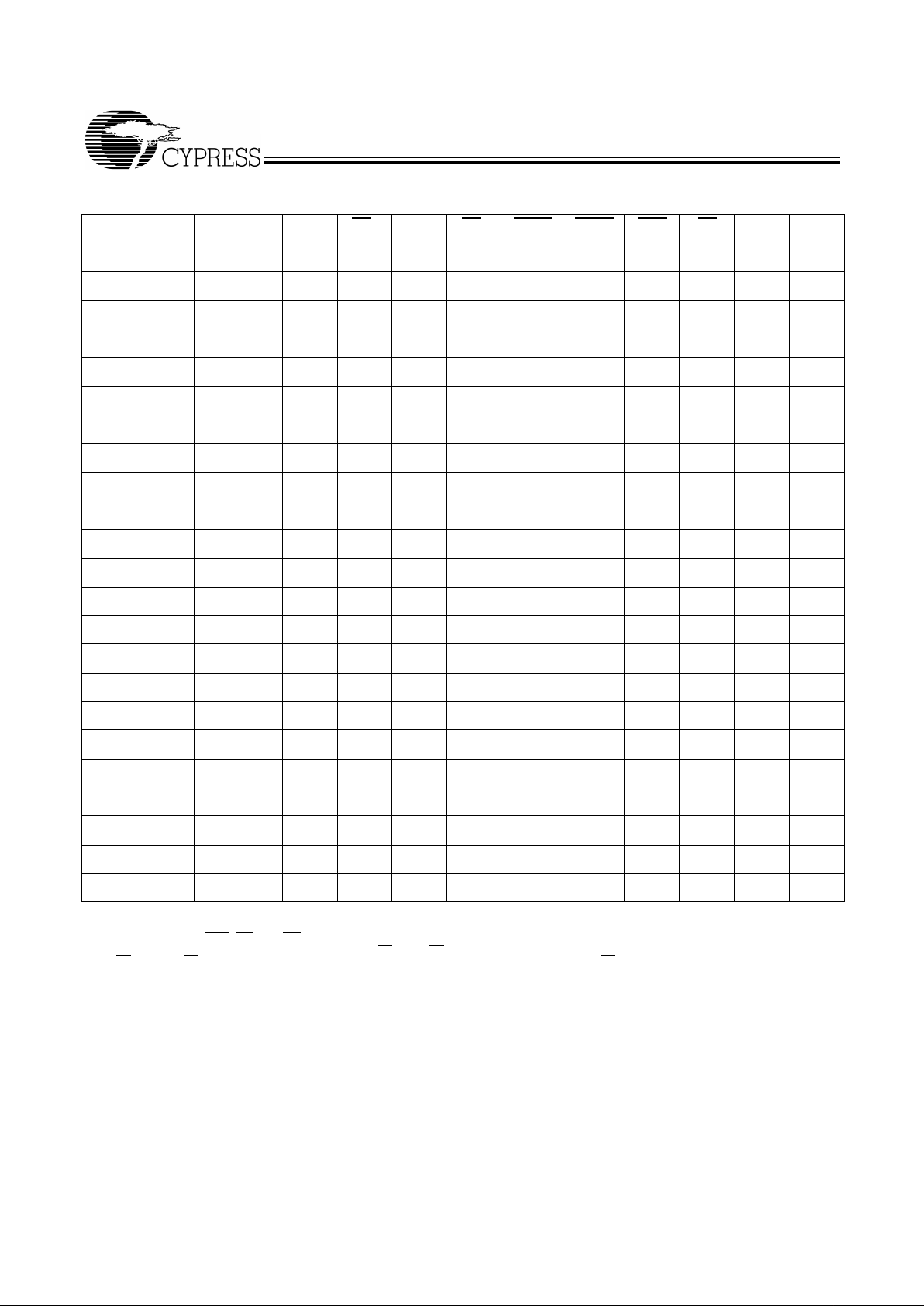
[1, 2, 3, 4]
Next Cycle Add. Used ZZ CE
3
CE
2
CE
1
ADSP ADSC ADV OE DQ Write
Unselected None 0 X X 1 X 0 X X Hi-Z X
Unselected None 0 1 X 0 0 X X X Hi-Z X
Unselected None 0 X 0 0 0 X X X Hi-Z X
Unselected None 0 1 X 0 1 0 X X Hi-Z X
Unselected None 0 X 0 0 1 0 X X Hi-Z X
Begin Read External 0 0 1 0 0 X X X Hi-Z X
Begin Read External 0 0 1 0 1 0 X X Hi-Z Read
Continue Read Next 0 X X X 1 1 0 1 Hi-Z Re ad
Continue Read Next 0 X X X 1 1 0 0 DQ Read
Continue Read Next 0 X X 1 X 1 0 1 Hi-Z Read
Continue Read Next 0 X X 1 X 1 0 0 DQ Read
Suspend Read Current 0 X X X 1 1 1 1 Hi-Z Read
Suspend Read Current 0 X X X 1 1 1 0 DQ Read
Suspend Read Current 0 X X 1 X 1 1 1 Hi-Z Read
Suspend Read Current 0 X X 1 X 1 1 0 DQ Read
Begin Write Current 0 X X X 1 1 1 X Hi-Z Write
Begin Write Current 0 X X 1 X 1 1 X Hi-Z Write
Begin Write External 0 0 1 0 1 0 X X Hi-Z Write
Continue Write Next 0 X X X 1 1 0 X Hi-Z Write
Continue Write Next 0 X X 1 X 1 0 X Hi-Z Write
Suspend Write Current 0 X X X 1 1 1 X Hi-Z Write
Suspend Write Current 0 X X 1 X 1 1 X Hi-Z Write
ZZ “sleep” None 1 X X X X X X X Hi-Z X
Notes:
1. X = “Don't Care,” 1 = HIGH, 0 = LOW.
2. Write is defined by BWE
, BWx, and GW. See Write Cycle Descriptions table.
3. The DQ pins are controlled by the current cycle and the OE
signal. OE is asynchronous and is not sampled with the clock.
4. CE1, CE2 and CE3 are available only in the TQFP package. The BGA package has a single chip select, CE1.
 Loading...