

r
CY2292
Three-PLL General-Purpose
EPROM Programmable Clock Generato
Features
• Three integrated phase-locked loops
• EPROM programmability
• Factory-programmable (CY2292) or field-programmable (CY2292F) device options
• Low-skew, low-jitter, high-accuracy outputs
• Power-management options (Shutdown, OE, Suspend)
• Frequency select option
• Smooth slewing on CPUCLK
• Configurable 3.3V or 5V operation
• 16-pin SOIC Package (TSSOP: F only)
Benefits
• Generates up to three custom frequencies from
external sources
• Easy customization and fast turnaround
• Programming support available for all opportunities
• Meets critical industry standard timing requirements
• Supports low-power applications
• Eight user-selectable frequencies on CPU PLL
• Allows downstream PLLs to stay locked on CPUCLK
output
• Enables application compatibility
• Industry-standard packaging saves on board space
Selector Guide
Part Number Outputs Input Frequency Range Output Frequency Range Specifics
CY2292 6 10 MHz–25 MHz (external crystal)
1 MHz–30 MHz (reference clock)
CY2292I 6 10 MHz–25 MHz (external crystal)
1 MHz–30 MHz (reference clock)
CY2292F 6 10 MHz–25 MHz (external crystal)
1 MHz–30 MHz (reference clock)
CY2292FI 6 10 MHz–25 MHz (external crystal)
1 MHz–30 MHz (reference clock)
CY2292FZ 6 10 MHz–25 MHz (external crystal)
1 MHz–30 MHz (reference clock)
76.923 kHz–100 MHz (5V)
76.923 kHz–80 MHz (3.3V)
76.923 kHz–90 MHz (5V)
76.923 kHz–66.6 MHz (3.3V)
76.923 kHz–90 MHz (5V)
76.923 kHz–66.6 MHz (3.3V)
76.923 kHz–80 MHz (5V)
76.923 kHz–60.0 MHz (3.3V)
76.923 kHz–90 MHz (5V)
76.923 kHz–66.6 MHz (3.3V)
Factory Programmable
Commercial Temperature
Factory Programmable
Industrial Temperature
Field Programmable
Commercial Temperature
Field Programmable
Industrial Temperature
Field Programmable
Commercial Temperature
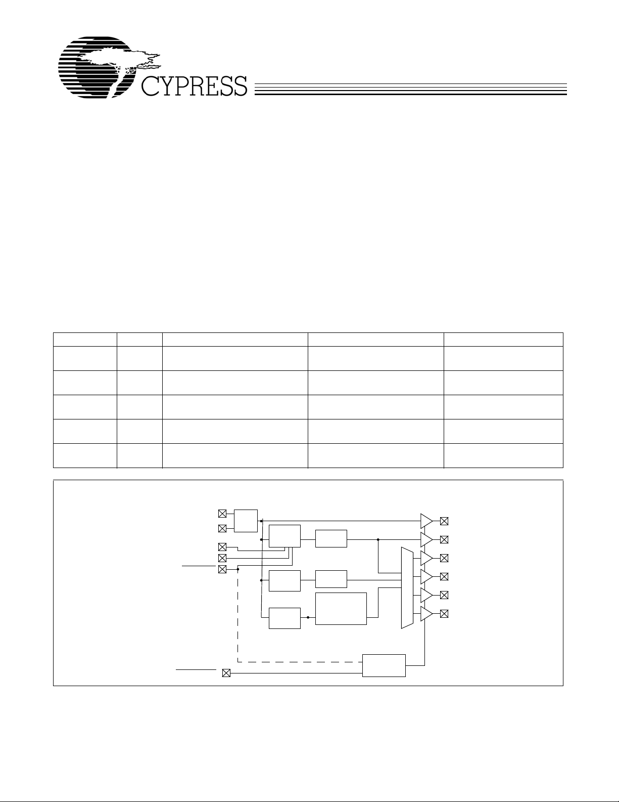
Logic Block Diagram
XTALIN
XTALOUT
S2/SUSPEND
SHUTDOWN
S0
S1
OE
.
OSC.
CPLL
(8 BIT)
UPLL
(10 BIT)
SPLL
(8 BIT)
/
/1,2,4
/1,2,4,8
/1,2,3,4,5,6
/8,10,12,13
/20,24,26,40
/48,52,96,104
CONFIG
EPROM
MUX
XBUF
CPUCLK
CLKA
CLKB
CLKC
CLKD
Cypress Semiconductor Corporation • 3901 North First Street • San Jose, CA 95134 • 408-943-2600
Document #: 38-07449 Rev. *B Revised October 12, 2004
CY2292
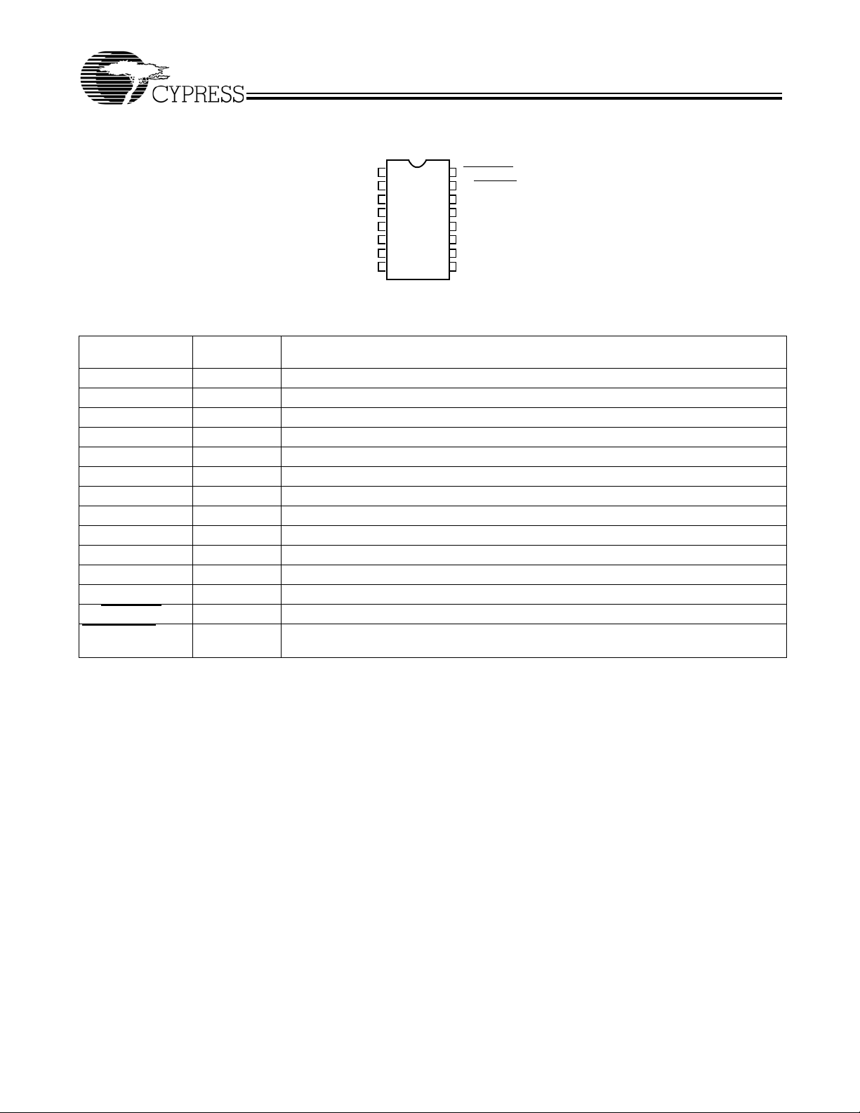
Pin Configurations
CY2292
16-pin SOIC
CLKC
V
DD
GND
XTALIN
XTALOUT
XBUF
CLKD
CPUCLK
1
2
3
4
5
6
7
8
16
15
14
13
12
11
10
9
Pin Summary
Name
CLKC 1 Configurable clock output C.
V
DD
GND 3, 11 Ground.
XTALIN
XTALOUT
[1]
[1, 2]
XBUF 6 Buffered reference clock output.
CLKD 7 Configurable clock output D.
CPUCLK 8 CPU frequency clock output.
CLKB 9 Configurable clock output B.
CLKA 10 Configurable clock output A.
S0 12 CPU clock select input, bit 0.
S1 13 CPU clock select input, bit 1.
S2/SUSPEND
SHUTDOWN/OE 16 Places outputs in three-state
Pin Number
CY2292 Description
2, 14 Voltage supply.
4 Reference crystal input or external reference clock input.
5 Reference crystal feedback.
15 CPU clock select input, bit 2. Optionally enables suspend feature when LOW.
[4]
places outputs in three-state
[4]
SHUTDOWN/OE
S2/SUSPEND
V
DD
S1
S0
GND
CLKA
CLKB
[3]
condition and shuts down chip when LOW. Optionally, only
condition and does not shut down chip when LOW.
Operation
this crystal. Alternatively, an external reference clock of
frequency between 1 MHz and 30 MHz can be used.
The CY2292 is a third-generation family of clock generators.
The CY2292 is upwardly compatible with the industry standard
Output Configuration
ICD2023 and ICD2028 and continues their tradition by
providing a high level of customizable features to meet the
diverse clock generation needs of modern motherboards and
other synchronous systems.
All parts provide a highly configurable set of clocks for PC
motherboard applications. Each of the four configurable clock
outputs (CLKA–CLKD) can be assigned 1 of 30 frequencies in
any combination. Multiple outputs configured for the same or
[3]
related
frequencies will have low (≤ 500 ps) skew, in effect
providing on-chip buffering for heavily loaded signals.
The CY2292 can be configured for either 5V or 3.3V operation.
The internal ROM tables use EPROM technology, allowing full
customization of output frequencies. The reference oscillator
has been designed for 10-MHz to 25-MHz crystals, providing
additional flexibility. No external components are required with
Notes:
1. For best accuracy, use a parallel-resonant crystal, C
2. Float XTALOUT pin if XTALIN is driven by reference clock (as opposed to crystal).
3. Please refer to application note “Understanding the CY2291, CY2292 and CY2295” for more information.
4. The CY2292 has weak pull-downs on all outputs. Hence, when a three-state condition is forced on the outputs, the output pins are pulled LOW.
≈ 17 pF or 18 pF.
LOAD
The CY2292 has four independent frequency sources on-chip.
These are the reference oscillator, and three Phase-Locked
Loops (PLLs). Each PLL has a specific function. The System
PLL (SPLL) provides fixed output frequencies on the config-
urable outputs. The SPLL offers the most output frequency
divider options. The CPU PLL (CPLL) is controlled by the
select inputs (S0–S2) to provide eight user-selectable
frequencies with smooth slewing between frequencies. The
Utility PLL (UPLL) provides the most accurate clock. It is often
used for miscellaneous frequencies not provided by the other
frequency sources.
All configurations are EPROM programmable, providing short
sample and production lead times. Please refer to the appli-
cation note Understanding the CY2291, CY2292, and CY2295
for information on configuring the part.
Document #: 38-07449 Rev. *B Page 2 of 11

CY2292
Power-Saving Features
The SHUTDOWN/OE input three-states the outputs when
pulled LOW. If system shutdown is enabled, a LOW on this pin
also shuts off the PLLs, counters, the reference oscillator, and
all other active components. The resulting current on the V
pins will be less than 50 µA (for commercial temperature or
100 µA for industrial temperature). After leaving shutdown
mode, the PLLs will have to relock. All outputs have a weak
pull-down so that the outputs do not float when three-stated.
The S2/SUSPEND input can be configured to shut down a
customizable set of outputs and/or PLLs, when LOW. All PLLs
and any of the outputs can be shut off in nearly any combination. The only limitation is that if a PLL is shut off, all outputs
derived from it must also be shut off. Suspending a PLL shuts
off all associated logic, while suspending an output simply
forces a three-state condition.
The CPUCLK can slew (transition) smoothly between 20 MHz
and the maximum output frequency (100 MHz at 5V/80 MHz
at 3.3V for Commercial Temp. parts or 90 MHz at 5V/66.6 MHz
at 3.3V for Industrial Temp. and for field-programmed parts).
This feature is extremely useful in “Green” PC and laptop
applications, where reducing the frequency of operation can
result in considerable power savings. This feature meets all
486 and Pentium
®
processor slewing requirements.
[3]
DD
[4]
CyClocks Software
CyClocks is an easy-to-use application that allows you to
configure any one of the EPROM-programmable clocks
offered by Cypress. You may specify the input frequency, PLL
and output frequencies, and different functional options.
Please note the output frequency ranges in this data sheet
when specifying them in CyClocks to ensure that you stay
within the limits. CyClocks also has a power calculation feature
that allows you to see the power consumption of your specific
configuration. You can download a copy of CyClocks for free
on Cypress’s web site at www.cypress.com.
Cypress FTG Programmer
The Cypress Frequency Timing Generator (FTG) Programmer
is a portable programmer designed to custom program our
family of EPROM Field Programmable Clock Devices. The
FTG programmers connect to a PC serial port and allow users
of CyClocks software to quickly and easily program any of the
CY2291F, CY2292F, CY2071AF, and CY2907F devices. The
ordering code for the Cypress FTG Programmer is CY3670.
Custom Configuration Request Procedure
The CY229x are EPROM-programmable devices that may be
configured in the factory or in the field by a Cypress Field Appli-
cation Engineer (FAE). The output frequencies requested will
be matched as closely as the internal PLL divider and multi-
plier options allow. All custom requests must be submitted to
your local Cypress FAE or sales representative. The method
to use to request custom configurations is:
Use CyClocks software. This software automatically calcu-
lates the output frequencies that can be generated by the
CY229x devices and provides a print-out of final pinout which
can be submitted (in electronic or print format) to your local
FAE or sales representative. The CyClocks software is
available free of charge from the Cypress web site
(http://www.cypress.com) or from your local sales represen-
tative.
Once the custom request has been processed you will receive
a part number with a 3-digit extension (e.g., CY2292SC-128)
specific to the frequencies and pinout of your device. This will
be the part number used for samples requests and production
orders.
Document #: 38-07449 Rev. *B Page 3 of 11
CY2292
Maximum Ratings
(Above which the useful life may be impaired. For user guidelines, not tested.)
Supply Voltage............................................... –0.5V to +7.0V
DC Input Voltage............................................–0.5V to +7.0V
Storage Temperature ................................. –65°C to +150°C
Max. Soldering Temperature (10 sec) ......................... 260°C
Junction Temperature .................................................. 150°C
Package Power Dissipation...................................... 750 mW
Static Discharge Voltage.............................................≤ 2000V
(per MIL-STD-883, Method 3015)
Operating Conditions
[5]
Parameter Description Part Numbers Min. Max. Unit
V
DD
V
DD
T
A
Supply Voltage, 5.0V operation All 4.5 5.5 V
Supply Voltage, 3.3V operation All 3.0 3.6 V
Commercial Operating Temperature, Ambient CY2292/CY2292F 0 +70 °C
Industrial Operating Temperature, Ambient CY2292I/CY2292FI −40 +85 °C
C
C
f
REF
LOAD
LOAD
Max. Load Capacitance 5.0V Operation All 25 pF
Max. Load Capacitance 3.3V Operation All 15 pF
External Reference Crystal All 10.0 25.0 MHz
External Reference Clock
[6, 7, 8]
All 1 30 MHz
Electrical Characteristics, Commercial 5.0V
Parameter Description Conditions Min. Typ. Max. Unit
V
V
V
V
I
IH
I
IL
I
OZ
I
DD
I
DDS
OH
OL
IH
IL
HIGH-Level Output Voltage IOH = 4.0 mA 2.4 V
LOW-Level Output Voltage IOL = 4.0 mA 0.4 V
[9]
[9]
Except crystal pins 2.0 V
Except crystal pins 0.8 V
– 0.5V <1 10 µA
DD
HIGH-Level Input Voltage
LOW-Level Input Voltage
Input HIGH Current VIN = V
Input LOW Current VIN = +0.5V <1 10 µA
Output Leakage Current Three-state outputs 250 µA
VDD Supply Current
VDD Power Supply Current in Shutdown Mode
[10]
Commercial VDD = VDD max., 5V operation 75 100 mA
[10]
Shutdown active CY2292/CY2292F 10 50 µA
Electrical Characteristics, Commercial 3.3V
Parameter Description Conditions Min. Typ. Max. Unit
V
OH
V
OL
V
IH
V
IL
I
IH
I
IL
I
OZ
I
DD
I
DDS
Notes:
5. Electrical parameters are guaranteed by design with these operating conditions, unless otherwise noted.
6. External input reference clock must have a duty cycle between 40% and 60%, measured at V
7. Please refer to application note “Crystal Oscillator Topics” for information on AC-coupling the external input reference clock.
8. The oscillator circuit is optimized for a crystal reference and for external reference clocks up to 20 MHz. For external reference clocks above 20 MHz, it is
recommended that a 150Ω pull-up resistor to V
9. Xtal inputs have CMOS thresholds.
10. Load = Max., V
formula (multiply by 0.65 for 3V operation): I
Document #: 38-07449 Rev. *B Page 4 of 11
HIGH-Level Output Voltage IOH = 4.0 mA 2.4 V
LOW-Level Output Voltage IOL = 4.0 mA 0.4 V
HIGH-Level Input Voltage
LOW-Level Input Voltage
Input HIGH Current VIN = V
[9]
[9]
Except crystal pins 2.0 V
Except crystal pins 0.8 V
– 0.5V < 1 10 µA
DD
Input LOW Current VIN = +0.5V < 1 10 µA
Output Leakage Current Three-state outputs 250 µA
VDD Supply Current
VDD Power Supply Current in Shutdown Mode
= 0V or VDD, Typical (–104) configuration, CPUCLK = 66 MHz. Other configurations will vary. Power can be approximated by the following
IN
[10]
Commercial VDD = VDD Max., 3.3V operation 50 65 mA
[10]
Shutdown active CY2292/CY2292F 10 50 µA
/2.
DD
be connected to the Xout pin.
DD
=10+0.06•(F
DD
CPLL+FUPLL
+2•F
SPLL
)+0.27•(F
CLKA+FCLKB+FCLKC+FCLKD+FCPUCLK+FXBUF
).

CY2292
Electrical Characteristics, Industrial 5.0V
Parameter Description Conditions Min. Typ. Max. Unit
V
OH
V
OL
V
IH
V
IL
I
IH
I
IL
I
OZ
I
DD
I
DDS
Electrical Characteristics, Industrial 3.3V
Parameter Description Conditions Min. Typ. Max. Unit
V
OH
V
OL
V
IH
V
IL
I
IH
I
IL
I
OZ
I
DD
I
DDS
HIGH-Level Output Voltage IOH = 4.0 mA 2.4 V
LOW-Level Output Voltage IOL = 4.0 mA 0.4 V
HIGH-Level Input Voltage
LOW-Level Input Voltage
Input HIGH Current VIN = V
[9]
[9]
Except crystal pins 2.0 V
Except crystal pins 0.8 V
– 0.5V <1 10 µA
DD
Input LOW Current VIN = +0.5V <1 10 µA
Output Leakage Current Three-state outputs 250 µA
VDD Supply Current
VDD Power Supply Current in
Shutdown Mode
[10]
Industrial VDD = VDD Max., 5V operation 75 110 mA
[10]
Shutdown active CY2292I/CY2292FI 10 100 µA
HIGH-Level Output Voltage IOH = 4.0 mA 2.4 V
LOW-Level Output Voltage IOL = 4.0 mA 0.4 V
HIGH-Level Input Voltage
LOW-Level Input Voltage
Input HIGH Current VIN = V
[9]
Except crystal pins 2.0 V
[9]
Except crystal pins 0.8 V
– 0.5V <1 10 µA
DD
Input LOW Current VIN = +0.5V <1 10 µA
Output Leakage Current Three-state outputs 250 µA
VDD Supply Current
[10]
Indus-
VDD = VDD Max., 3.3V operation 50 70 mA
trial
VDD Power Supply Current in
Shutdown Mode
[10]
Shutdown active CY2292I/CY2292FI 10 100 µA
Switching Characteristics, Commercial 5.0V
Parameter Name Description Min. Typ. Max. Unit
t
1
t
3
t
4
t
5
t
6
t
7
t
8
Notes:
11. XBUF duty cycle depends on XTALIN duty cycle.
12. Measured at 1.4V.
13. Measured between 0.4V and 2.4V.
14. Jitter varies with configuration. All standard configurations sample tested at the factory conform to this limit. For more information on jitter, please refer to the
application note: Jitter in PLL-Based Systems.
Output Period Clock output range, 5V
operation
Output Duty Cycle
[11]
Duty cycle for outputs, defined as t2 ÷ t
f
> 66 MHz
OUT
Duty cycle for outputs, defined as t
f
< 66 MHz
OUT
Rise Time Output clock rise time
Fall Time Output clock fall time
Output Disable Time Time for output to enter three-state mode
after SHUTDOWN
/OE goes LOW
Output Enable Time Time for output to leave three-state mode
after SHUTDOWN
Skew Skew delay between any identical or
related outputs
/OE goes HIGH
[3, 12, 14]
CY2292 10
CY2292F 11.1
1
÷ t
2
1
[13]
[13]
[12]
[12]
(100 MHz)
(90 MHz)
(76.923 kHz)
(76.923 kHz)
40% 50% 60%
45% 50% 55%
35ns
2.5 4 ns
10 15 ns
10 15 ns
< 0.25 0.5 ns
13000
13000
ns
ns
CPUCLK Slew Frequency transition rate 1.0 20.0 MHz/ms
Document #: 38-07449 Rev. *B Page 5 of 11

CY2292
Switching Characteristics, Commercial 5.0V (continued)
Parameter Name Description Min. Typ. Max. Unit
[11]
[14]
[14]
[14]
[14]
[14]
[14]
[14]
[14]
Peak-to-peak period jitter (t9A max. – t9A
min.), % of clock period (f
OUT
< 4 MHz)
Peak-to-peak period jitter (t9B max. – t9B
<0.5 1 %
<0.7 1 ns
min.)
(4 MHz <
Peak-to-peak period jitter (16 MHz < f
50 MHz)
Peak-to-peak period jitter (f
f
OUT
< 16 MHz)
OUT <
> 50 MHz) <250 350 ps
OUT
<400 500 ps
Lock Time from Power-up <0.25 1 ms
CY2292F 20 90 MHz
CY2292 12.5
operation
CY2292F 15
Duty cycle for outputs, defined as t2 ÷ t
f
> 66 MHz
OUT
Duty cycle for outputs, defined as t
f
< 66 MHz
OUT
[13]
[13]
[12]
1
[12]
÷ t
2
1
Time for output to enter three-state mode after
SHUTDOWN
/OE goes LOW
Time for output to leave three-state mode after
SHUTDOWN
outputs
/OE goes HIGH
[3, 12, 14]
Peak-to-peak period jitter (t9A max. – t9A min.),
% of clock period (f
OUT
< 4 MHz)
Peak-to-peak period jitter (t9B max. – t9B min.)
f
(4 MHz <
Peak-to-peak period jitter (16 MHz < f
Peak-to-peak period jitter (f
OUT
< 16 MHz)
50 MHz) < 400 500 ps
OUT <
> 50 MHz) < 250 350 ps
OUT
(80 MHz)
(66.6 MHz)
40% 50% 60%
45% 50% 55%
35ns
2.54ns
10 15 ns
10 15 ns
< 0.25 0.5 ns
< 0.5 1 %
< 0.7 1 ns
13000
(76.923 kHz)
13000
(76.923 kHz)
Lock Time from Power-up < 0.25 1 ms
CY2292F 20 66.6 MHz
t
t
t
t
t
t
9A
9B
9C
9D
10A
10B
Clock Jitter
Clock Jitter
Clock Jitter
Clock Jitter
Lock Time for CPLL Lock Time from Power-up <25 50 ms
Lock Time for UPLL and
SPLL
Slew Limits CPU PLL Slew Limits CY2292 20 100 MHz
Switching Characteristics, Commercial 3.3V
Parameter Name Description Min. Typ. Max. Unit
t
t
t
t
t
t
t
t
t
t
t
t
t
1
3
4
5
6
7
8
9A
9B
9C
9D
10A
10B
Output Period Clock output range, 3.3V
Output Duty
Cycle
Rise Time Output clock rise time
Fall Time Output clock fall time
Output Disable
Time
Output Enable
Time
Skew Skew delay between any identical or related
CPUCLK Slew Frequency transition rate 1.0 20.0 MHz/
Clock Jitter
Clock Jitter
Clock Jitter
Clock Jitter
Lock Time for CPLL Lock Time from Power-up < 25 50 ms
Lock Time for
UPLL and SPLL
Slew Limits CPU PLL Slew Limits CY2292 20 80 MHz
ns
ns
ms
Document #: 38-07449 Rev. *B Page 6 of 11

CY2292
Switching Characteristics, Industrial 5.0V
Parameter Name Description Min. Typ. Max. Unit
t
t
t
t
t
t
t
t
t
t
t
t
t
1
3
4
5
6
7
8
9A
9B
9C
9D
10A
10B
Output Period Clock output range, 5V
operation
Output Duty
[11]
Cycle
Duty cycle for outputs, defined as t2 ÷ t
f
> 66 MHz
OUT
Duty cycle for outputs, defined as t2 ÷ t
f
< 66 MHz
OUT
Rise Time Output clock rise time
Fall Time Output clock fall time
Output Disable
Time
Output Enable
Time
Skew Skew delay between any identical or related
Time for output to enter three-state mode after
SHUTDOWN
/OE goes LOW
Time for output to leave three-state mode after
SHUTDOWN
outputs
/OE goes HIGH
[3, 12, 14]
CY2292I 11.1
CY2292FI 12.5
[12]
1
[12]
1
[13]
[13]
(90 MHz)
(80 MHz)
(76.923 kHz)
(76.923 kHz)
40% 50% 60%
45% 50% 55%
35ns
2.54ns
10 15 ns
10 15 ns
< 0.25 0.5 ns
13000
13000
CPUCLK Slew Frequency transition rate 1.0 20.0 MHz/
Clock Jitter
Clock Jitter
Clock Jitter
Clock Jitter
[14]
[14]
[14]
[14]
Peak-to-peak period jitter (t9A max. – t9A min.), %
of clock period (f
OUT
< 4 MHz)
Peak-to-peak period jitter (t9B max. – t9B min.) (4
MHz <
f
< 16 MHz)
OUT
Peak-to-peak period jitter (16 MHz < f
Peak-to-peak period jitter (f
> 50 MHz) < 250 350 ps
OUT
50 MHz) < 400 500 ps
OUT <
< 0.5 1 %
< 0.7 1 ns
Lock Time for CPLL Lock Time from Power-up <25 50 ms
Lock Time for
Lock Time from Power-up <0.25 1 ms
UPLL and SPLL
Slew Limits CPU PLL Slew Limits CY2292I 20 90 MHz
CY2292FI 20 80 MHz
ns
ns
ms
Switching Characteristics, Industrial 3.3V
Parameter Name Description Min. Typ. Max. Unit
t
1
t
3
t
4
t
5
t
6
t
7
t
8
Document #: 38-07449 Rev. *B Page 7 of 11
Output Period Clock output range, 3.3V
operation
Output Duty
[11]
Cycle
Duty cycle for outputs, defined as t2 ÷ t
f
> 66 MHz
OUT
Duty cycle for outputs, defined as t
f
< 66 MHz
OUT
Rise Time Output clock rise time
Fall Time Output clock fall time
Output Disable
Time
Output Enable
Time
Skew Skew delay between any identical or related
Time for output to enter three-state mode after
SHUTDOWN
/OE goes LOW
Time for output to leave three-state mode after
SHUTDOWN
outputs
/OE goes HIGH
[3, 12, 14]
CY2292I 15
CY2292FI 16.66
[12]
1
[12]
÷ t
2
1
[13]
[13]
(66.6 MHz)
(60 MHz)
40% 50% 60%
45% 50% 55%
35 ns
2.5 4 ns
10 15 ns
10 15 ns
< 0.25 0.5 ns
13000
(76.923 kHz)
13000
(76.923 kHz)
ns
ns
CPUCLK Slew Frequency transition rate 1.0 20.0 MHz/ms

CY2292
Switching Characteristics, Industrial 3.3V (continued)
Parameter Name Description Min. Typ. Max. Unit
t
t
t
t
t
t
9A
9B
9C
9D
10A
10B
Clock Jitter
Clock Jitter
Clock Jitter
Clock Jitter
Lock Time for
CPLL
Lock Time for
UPLL and SPLL
Slew Limits CPU PLL Slew Limits CY2292I 20 66.6 MHz
Switching Waveforms
All Outputs, Duty Cycle and Rise/Fall Time
[14]
[14]
[14]
[14]
Peak-to-peak period jitter (t9A max. – t9A min.),
% of clock period (f
OUT
< 4 MHz)
Peak-to-peak period jitter (t9B max. – t9B min.)
(4 MHz <
f
OUT
< 16 MHz)
Peak-to-peak period jitter
(16 MHz < f
OUT <
50 MHz)
Peak-to-peak period jitter
(f
> 50 MHz)
OUT
< 0.5 1 %
< 0.7 1 ns
< 400 500 ps
< 250 350 ps
Lock Time from Power-up < 25 50 ms
Lock Time from Power-up < 0.25 1 ms
CY2292FI 20 60 MHz
t
1
t
2
OUTPUT
t
3
Output Three-State Timing
OE
THREE-STATE
ALL
OUTPUTS
CLK Outputs Jitter and Skew
CLK
OUTPUT
RELATED
CLK
CPU Frequency Change
SELECT
OLD SELECT NEW SELECT STABLE
F
old
t
4
[4]
t
5
t
9A
t
7
t8&t
10
F
new
t
6
CPU
Document #: 38-07449 Rev. *B Page 8 of 11

CY2292
Test Circuit
V
DD
V
0.1 µF
DD
OUTPUTS
0.1 µF
GND
Package Characteristics
Package θJA (C/W) θJC (C/W) Transistor Count
16-pin SOIC 83 19 9271
Ordering Information
Ordering Code Package Type Operating Range Operating Voltage
CY2292SC–XXX 16-Pin SOIC Commercial 5.0V
CY2292SC–XXXT 16-Pin SOIC – Tape and Reel Commercial 5.0V
CY2292SL–XXX 16-Pin SOIC Commercial 3.3V
CY2292SL–XXXT 16-Pin SOIC – Tape and Reel Commercial 3.3V
CY2292F 16-Pin SOIC Commercial 3.3V or 5.0V
CY2292FT 16-Pin SOIC – Tape and Reel Commercial 3.3V or 5.0V
CY2292SI–XXX 16-Pin SOIC Industrial 3.3V or 5.0V
CY2292SI–XXXT 16-Pin SOIC – Tape and Reel Industrial 3.3V or 5.0V
CY2292FI 16-Pin SOIC Industrial 3.3V or 5.0V
CY2292FIT 16-Pin SOIC – Tape and Reel Industrial 3.3V or 5.0V
CY2292FZ 16-Pin TSSOP Commercial 3.3V or 5.0V
CY2292FZT 16-Pin SOIC – Tape and Reel Commercial 3.3V or 5.0V
Lead-Free
CY2292SXC–XXX 16-Pin SOIC Commercial 5.0V
CY2292SXC–XXXT 16-Pin SOIC – Tape and Reel Commercial 5.0V
CY2292SXL–XXX 16-Pin SOIC Commercial 3.3V
CY2292SXL–XXXT 16-Pin SOIC – Tape and Reel Commercial 3.3V
CY2292FXC 16-Pin SOIC Commercial 3.3V or 5.0V
CY2292FXCT 16-Pin SOIC – Tape and Reel Commercial 3.3V or 5.0V
CY2292SXI–XXX 16-Pin SOIC Industrial 3.3V or 5.0V
CY2292SXI–XXXT 16-Pin SOIC – Tape and Reel Industrial 3.3V or 5.0V
CY2292FXI 16-Pin SOIC Industrial 3.3V or 5.0V
CY2292FXIT 16-Pin SOIC – Tape and Reel Industrial 3.3V or 5.0V
CY2292FZX 16-Pin TSSOP Commercial 3.3V or 5.0V
CY2292FZXT 16-Pin SOIC – Tape and Reel Commercial 3.3V or 5.0V
CLK out
C
LOAD
Document #: 38-07449 Rev. *B Page 9 of 11

Package Diagrams
CY2292
16 Lead (150 Mil) SOIC
16-Lead (150-Mil) SOIC S16.15
PIN 1 ID
18
0.150[3.810]
0.157[3.987]
0.230[5.842]
0.244[6.197]
916
0.050[1.270]
BSC
0.386[9.804]
0.393[9.982]
0.0138[0.350]
0.0192[0.487]
0.061[1.549]
0.068[1.727]
0.004[0.102]
0.0098[0.249]
SEATING PLANE
0.004[0.102]
DIMENSIONS IN INCHES[MM] MIN.
REFERENCE JEDEC MS-012
PACKAGE WEIGHT 0.15gms
S16.15 STANDARD PKG.
SZ16.15 LEAD FREE PKG.
0°~8°
0.016[0.406]
0.035[0.889]
PART #
0.010[0.254]
0.016[0.406]
MAX.
X 45°
0.0075[0.190]
0.0098[0.249]
51-85068-*B
16-lead TSSOP 4.40 MM Body Z16.173
1
PIN1ID
DIMENSIONS IN MM[INCHES] MIN.
MAX.
REFERENCE JEDEC MO-153
4.30[0.169]
4.50[0.177]
6.25[0.246]
6.50[0.256]
PACKAGE WEIGHT 0.05 gms
PART #
Z16.173 STANDARD PKG.
ZZ16.173 LEAD FREE PKG.
16
0.65[0.025]
0.85[0.033]
0.95[0.037]
BSC.
4.90[0.193]
5.10[0.200]
0.19[0.007]
0.30[0.012]
0.05[0.002]
0.15[0.006]
1.10[0.043] MAX.
0.076[0.003]
SEATING
PLANE
GAUGE
PLANE
0.25[0.010]
BSC
0°-8°
0.50[0.020]
0.70[0.027]
0.09[[0.003]
0.20[0.008]
51-85091-*A
CyClocks is a trademark of Cypress Semiconductor Corporation.Pentium is a registered trademark of Intel Corporation.
All product and company names mentioned in this document may be the trademarks of their respective holders.
Document #: 38-07449 Rev. *B Page 10 of 11
© Cypress Semiconductor Corporation, 2004. The information contained herein is subject to change without notice. Cypress Semiconductor Corporation assumes no responsibility for the use
of any circuitry other than circuitry embodied in a Cypress product. Nor does it convey or imply any license under patent or other rights. Cypress products are not warranted nor intended to be
used for medical, life support, life saving, critical control or safety applications, unless pursuant to an express written agreement with Cypress. Furthermore, Cypress does not authorize its
products for use as critical components in life-support systems where a malfunction or failure may reasonably be expected to result in significant injury to the user. The inclusion of Cypress
products in life-support systems application implies that the manufacturer assumes all risk of such use and in doing so indemnifies Cypress against all charges.

Document History Page
Document Title: CY2292 Three-PLL General-Purpose EPROM Programmable Clock Generator
Document Number: 38-07449
REV. ECN NO. Issue Date
** 116993 07/01/02 DSG Changed from Spec number: 38-00946 to 38-07449
*A 119639 12/05/02 CKN Changed 8 MHz to 20 MHz in Power-saving Features
*B 277130 See ECN RGL Added Lead-free Devices
Orig. of
Change Description of Change
CY2292
Document #: 38-07449 Rev. *B Page 11 of 11
 Loading...