


Three-PLL Serial-Programmable
Flash-Programmable Clock Generator
CY22395
CY22393
CY22394
http://www.xinpian.net
提供单片机解密、IC解密、芯片解密业务
010-62245566 13810019655
Features
• Three integrated phase-locked loops (PLLs)
• Ultra wide divide counters (8-bit Q, 11-bit P, and 7-bit post
divide)
• Improved linear crystal load capacitors
• Flash programmability with external programmer
• Field-programmable
• Low jitter, high accuracy outputs
• Power management options (Shutdown, OE, Suspend)
• Configurable crystal drive strength
• Frequency select via three external LVTTL inputs
• 3.3V operation
• 16-pin TSSOP package
• CyClocksRT™ software support
Advanced Features
•I2C serial interface for in-system configurability
• Configurable output buffer
• Digital VCXO
• High frequency LVPECL output (CY22394 only)
• 3.3/2.5V outputs (CY22395 only)
Benefits
• Generates up to three unique frequencies on up to six
outputs from an external source.
• Allows for 0 ppm frequency generation and frequency
conversion in the most demanding applications.
• Improves frequency accuracy over temperature, age,
process, and initial ppm offset.
• Nonvolatile programming enables easy customization,
ultra-fast turnaround, perfor mance tweaking, design timing
margin testing, inventory control, lower part count, and more
secure product supply. In addition, any part in the family can
be programmed multiple times, which reduces
programming errors and provides an easy upgrade path for
existing designs.
• In-house programming of samples and prototype quantities
is available using the CY3672 FTG Development Kit.
Production quantities are available through Cypress
Semiconductor’s value-added distribu tion partners or by
using third-party programmers from BP Microsystems, HiLo
Systems, and others.
• Performance suitable for high-end multimedia, communications, industrial, A/D converters, and consumer applications.
• Supports numerous low power application schemes and
reduces electromagnetic interference (EMI) by allowing
unused outputs to be turned off.
• Adjust crystal drive strength for compatibility with virtually
all crystals.
• 3-bit external frequency select options for PLL1, CLKA, and
CLKB.
• Industry standard packaging saves on board space.
• Easy to use software support for design entry.
2
•I
C interface allows in-system programming into volatile
configuration memory. All frequency settings can be
changed, providing literally millions of frequency options.
• Adjust output buffer strength to lower EMI or improve timing
margin.
• Fine tune crystal oscillator frequency by changing load
capacitance.
• Differential output up to 400 MHz.
• Provides interfacing option for low voltage parts.
Cypress Semiconductor Corporation • 198 Champion Court • San Jose, CA 95134-1709 • 408-943-2600
Document #: 38-07186 Rev. *C Revised March 13, 2007
[+] Feedback [+] Feedback
CY22395
CY22394
CY22393
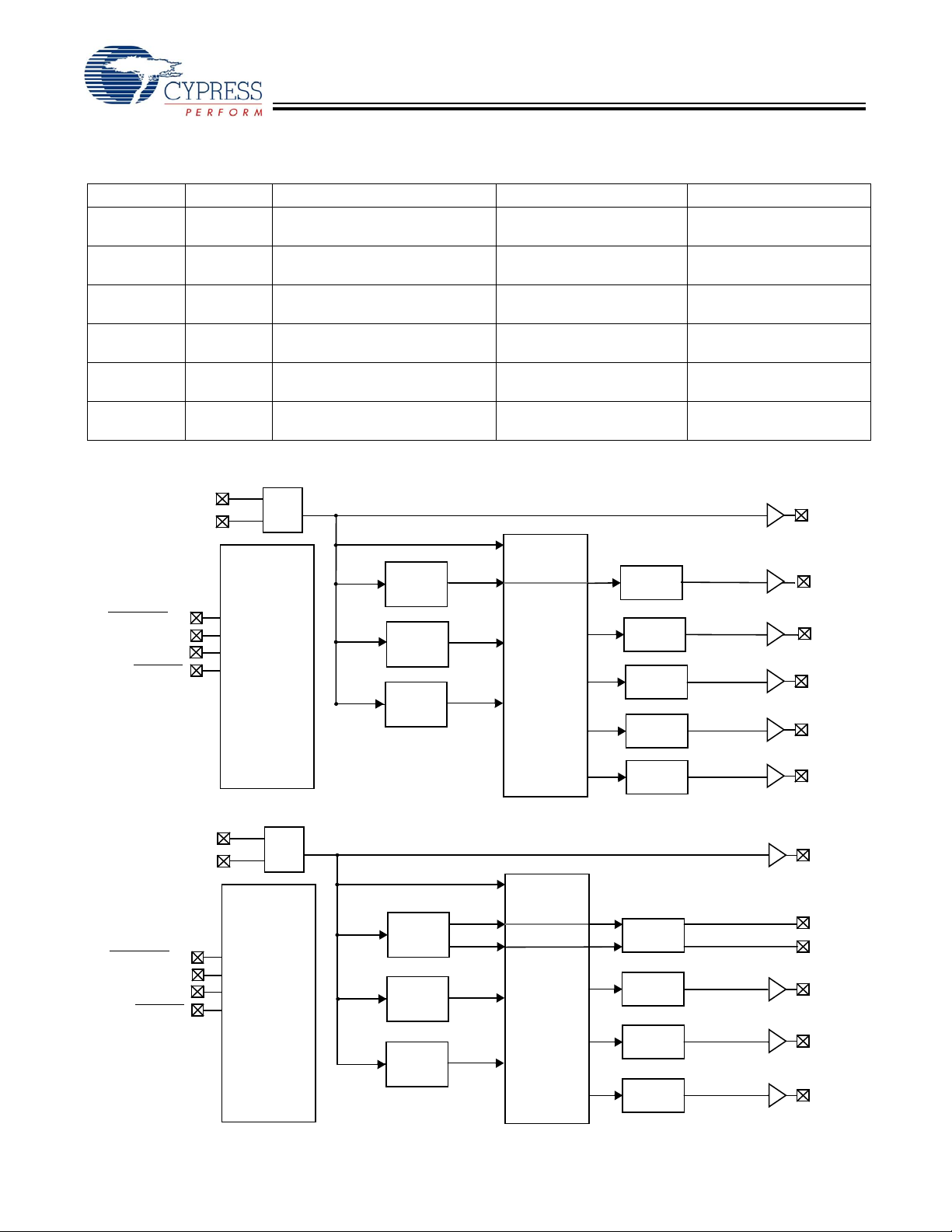
Logic Block Diagram — CY22393
XTALIN
XTALOUT
S2/SUSPEND
SDAT
SCLK
SHUTDOWN
/OE
CONFIGURATION
FLASH
OSC.
XBUF
PLL1
CLKE
11-Bit P
8-Bit Q
PLL2
11-Bit P
8-Bit Q
PLL3
11-Bit P
8-Bit Q
4x4
Switch
Crosspoint
Divider
/2, /3, or /4
Divider
7-Bit
Divider
7-Bit
Divider
7-Bit
Divider
7-Bit
CLKA
CLKB
CLKC
CLKD
Logic Block Diagram — CY22394
XTALIN
XTALOUT
S2/SUSPEND
SDAT
SCLK
SHUTDOWN
/OE
CONFIGURATION
FLASH
OSC.
XBUF
PLL1
P+CLK
11-Bit P
8-Bit Q
PLL2
11-Bit P
8-Bit Q
PLL3
11-Bit P
8-Bit Q
4x4
Switch
Crosspoint
Divider
7-Bit
Divider
7-Bit
Divider
7-Bit
PECL
OUTPUT
CLKA
CLKB
CLKC
P-CLK
0º
180º
http://www.xinpian.net
提供单片机解密、IC解密、芯片解密业务
010-62245566 13810019655
Selector Guide
Part Number Outputs Input Frequency Range Output Frequency Range Specifics
CY22393FC 6 CMOS 8 MHz–30 MHz (external crystal)
1 MHz–166 MHz (reference clock)
CY22393FI 6 CMOS 8 MHz–30 MHz (external crystal)
1 MHz–150 MHz (reference clock)
CY22394FC 1 PECL/
4 CMOS
CY22394FI 1 PECL/
4 CMOS
CY22395FC 4 LVCMOS/
1 CMOS
CY22395FI 4 LVCMOS/
1 CMOS
8 MHz–30 MHz (external crystal)
1 MHz–166 MHz (reference clock)
8 MHz–30 MHz (external crystal)
1 MHz–150 MHz (reference clock)
8 MHz–30 MHz (external crystal)
1 MHz–166 MHz (reference clock)
8 MHz–30 MHz (external crystal)
1 MHz–150 MHz (reference clock)
Up to 200 MHz Commercial Temperature
Up to 166 MHz Industrial Temperature
100 MHz–400 MHz (PECL)
Commercial Temperature
Up to 200 MHz (CMOS)
125 MHz–375 MHz (PECL)
Industrial Temperature
Up to 166 MHz (CMOS)
Up to 200 MHz (3.3V)
Commercial Temperature
Up to 133 MHz (2.5V)
Up to 166 MHz (3.3V)
Industrial Temperature
Up to 133 MHz (2.5V)
Document #: 38-07186 Rev. *C Page 2 of 17
[+] Feedback [+] Feedback
CY22395
CY22394
CY22393
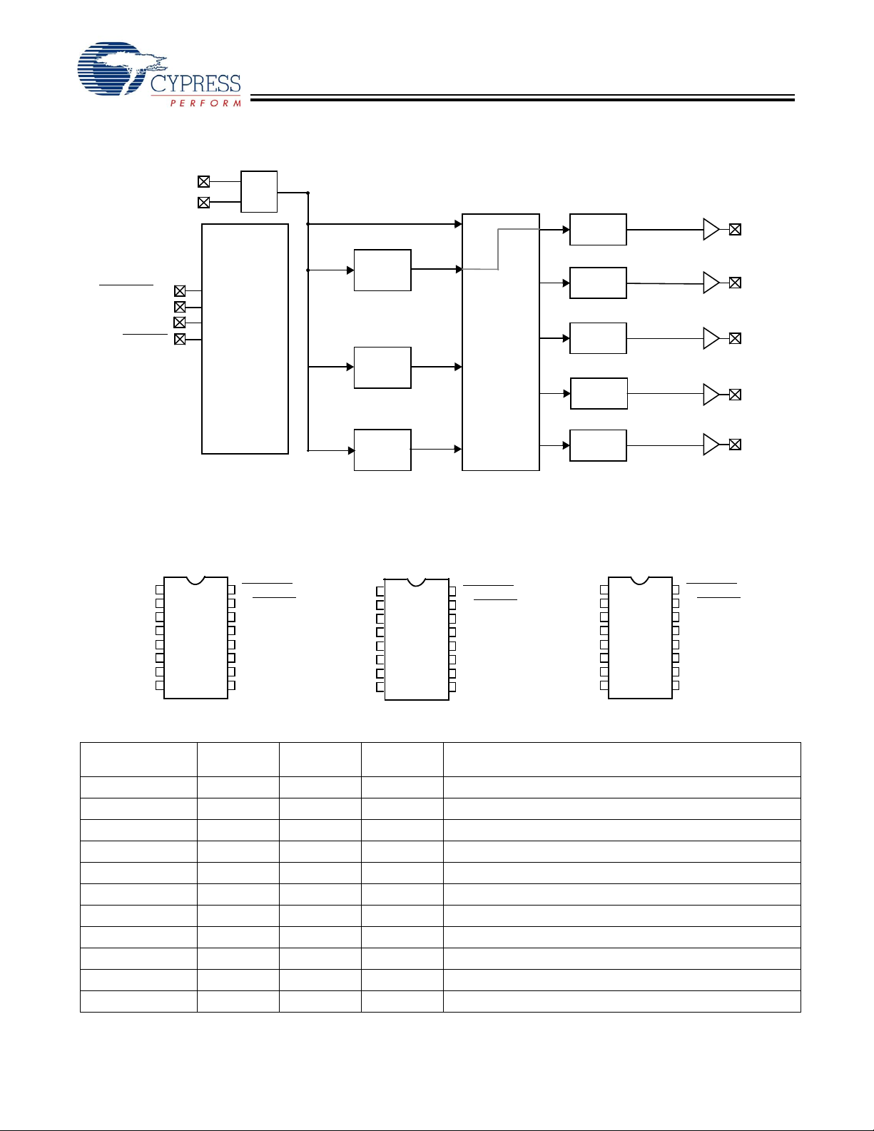
Logic Block Diagram — CY22395
XTALIN
XTALOUT
S2/SUSPEND
SDAT
SCLK
SHUTDOWN
/OE
CONFIGURATION
FLASH
OSC.
PLL1
LCLKE
11-Bit P
8-Bit Q
PLL2
11-Bit P
8-Bit Q
PLL3
11-Bit P
8-Bit Q
4x4
Switch
Crosspoint
Divider
7-Bit
Divider
7-Bit
Divider
7-Bit
Divider
7-Bit
Divider
/2, /3, or /4
LCLKA
LCLKB
CLKC
LCLKD
LCLKA, LCLKB, LCLKD, LCLKE referenced to LVDD
Pin Configurations
1
2
3
4
5
6
7
8
9
10
CLKC
V
DD
AGND
XTALIN
XTALOUT
XBUF
CLKD
CLKE
SHUTDOWN/OE
S2/SUSPEND
AV
DD
SCLK (S1)
SDAT (S0)
GND
CLKA
CLKB
16-pin TSSOP
11
12
13
14
15
16
CY22393
1
2
3
4
5
6
7
8
9
10
CLKC
V
DD
AGND
XTALIN
XTALOUT
XBUF
P–CLK
P+ CLK
SHUTDOWN/OE
S2/SUSPEND
AV
DD
SCLK (S1)
SDAT (S0)
GND
CLKA
CLKB
16-pin TSSOP
11
12
13
14
15
16
CY22394
1
2
3
4
5
6
7
8
9
10
CLKC
V
DD
AGND
XTALIN
XTALOUT
LCLKD
LCLKE
SHUTDOWN/OE
S2/SUSPEND
AV
DD
SCLK (S1)
SDAT (S0)
GND/LGND
LCLKA
LCLKB
16-pin TSSOP
11
12
13
14
15
16
CY22395
LV
DD
http://www.xinpian.net
提供单片机解密、IC解密、芯片解密业务
010-62245566 13810019655
Pin Definitions
Name
CLKC 1 1 1 Configurable clock output C
V
DD
AGND 3 3 3 Analog Ground
XTALIN 4 4 4 Reference crystal input or external reference clock input
XTALOUT 5 5 5 Reference crystal feedback
XBUF 6 6 N/A Buffered reference clock output
LV
DD
CLKD or LCLKD 7 N/A 7 Configurable clock output D; LCLKD referenced to LVDD
P– CLK N/A 7 N/A LV PECL output
CLKE or LCLKE 8 N/A 8 Configurable clock output E; LCLKE referenced to LVDD
P+ CLK N/A 8 N/A LV PECL output
Note
Document #: 38-07186 Rev. *C Page 3 of 17
1. LVPECL outputs requir e an external termination network.
Pin Number
CY22393
2 2 2 Power supply
N/A N/A 6 Low voltage clock output power supply
Pin Number
CY22394
Pin Number
CY22395
Description
[1]
[1]
[+] Feedback [+] Feedback
CY22395
CY22394
Pin Definitions (continued)
http://www.xinpian.net
提供单片机解密、IC解密、芯片解密业务
010-62245566 13810019655
CY22393
Name
CLKB or LCLKB 9 9 9 Configurable clock output B; LCLKB referenced to LVDD
CLKA or LCLKA 10 10 10 Configurable clock output A; LCLKA referenced to LVDD
GND/LGND 11 11 11 Ground
SDAT (S0) 12 12 12 Serial Port (I2C) Data. S0 value latched during start up
SCLK (S1) 13 13 13 Serial Port (I2C) Clock. S1 value latched during start up
AV
DD
S2/
SUSPEND
SHUTDOWN/
OE
Pin Number
CY22393
14 14 14 Analog Power Supply
15 15 15 General purpose input for frequency control; bit 2. Optionally,
16 16 16 Places outputs in tri-state condition and shuts down chip when
Operation
The CY22393, CY22394, and CY22395 are a family of parts
designed as upgrades to the existing CY22392 device. These
parts have similar performance to the CY22392, but provide
advanced features to meet the needs of more demanding
applications.
The clock family has three PLLs which, when combi ned with
the reference, allow up to four independent frequencies to be
output on up to six pins. These three PLLs are completely
programmable.
Configurable PLLs
PLL1 generates a frequency that is equal to the reference
divided by an 8-bit divider (Q) and multiplied by an 11-bit
divider in the PLL feedback loop (P). The output of PLL1 is sent
to two locations: the cross point switch and the PECL output
(CY22394). The output of PLL1 is also sent to a /2, /3, or /4
synchronous post-divider that is output through CLKE. The
frequency of PLL1 can be changed using serial programming
or by external CMOS inputs, S0, S1, and S2. See the following
section on General Purpose Inputs for more detail.
PLL2 generates a frequency that is equal to the reference
divided by an 8-bit divider (Q) and multiplied by an 11-bit
divider in the PLL feedback loop (P). The output of PLL2 is sent
to the cross point switch. The frequency of PLL2 is changed
using serial programming.
PLL3 generates a frequency that is equal to the reference
divided by an 8-bit divider (Q) and multiplied by an 11-bit
divider in the PLL feedback loop (P). The output of PLL3 is sent
to the cross point switch. The frequency of PLL3 is changed
using serial programming.
General Purpose Inputs
S2 is a general purpose input that is programmed to allow for
two different frequency settings. Options that switches with
this general purpose input are as follows: the frequency of
PLL1, the output divider of CLKB, and the output divi der of
CLKA.
Pin Number
CY22394
Pin Number
CY22395
Description
Suspend mode control input
LOW. Optionally , only places outputs in tri-state condition and
does not shut down chip when LOW
The two frequency settings are contained within an eight-row
frequency table. The values of SCLK (S1) and SDAT (S0) pins
are latched during start up and used as the other two indexes
into this array.
CLKA and CLKB have seven-bit dividers that point to one of
the two programmable settings (register 0 and register 1). Both
clocks share a single register control and both must be set to
register 0, or both must be set to register 1.
For example, the part may be programmed to use S0, S1, and
S2 (0,0,0 to 1,1,1) to control eight different values of P and Q
on PLL1. For each PLL1 P and Q setting, one of the two CLKA
and CLKB divider registers can be chosen. Any divider change
as a result of switching S0, S1, or S2 is guaranteed to be glitch
free.
Crystal Input
The input crystal oscillator is an important feature of this family
of parts because of its flexibility and performance features.
The oscillator inverter has programmable drive strength. This
allows for maximum compatibility with crystals from various
manufacturers, process, performance, and quality.
The input load capacitors are placed on-die to reduce external
component cost. These capacitors are true parallel-plate
capacitors for ultra-linear performance. These were chosen to
reduce the frequency shift that occurs when nonlinear load
capacitance interacts with load, bias, supply, and temperature
changes. Nonlinear (FET gate) crystal load capacitors should
not be used for MPEG, POTS dial tone, co mmunications, or
other applications that are sensitive to absolute frequency
requirements.
The value of the load capacitors is determined by six bits in a
programmable register. The load capacitance can be set with
a resolution of 0.375 pF for a total crystal load range of 6 pF
to 30 pF.
For driven clock inputs, the input load capacitors can be
completely bypassed. This allows the clock chip to accept
driven frequency inputs up to 166 MHz. If the application
requires a driven input, leave XTALOUT floating.
Document #: 38-07186 Rev. *C Page 4 of 17
[+] Feedback [+] Feedback

CY22395
CY22394
CY22393
http://www.xinpian.net
提供单片机解密、IC解密、芯片解密业务
010-62245566 13810019655
Digital VCXO
The serial programming interface is used to dynamically
change the capacitor load value on the crystal. A change in
crystal load capacitance corresponds with a change in the
reference frequency.
For special pullable crystals specified by Cypress, the capacitance pull range is +150 ppm to –150 ppm from midrange.
Be aware that adjusting the frequency of the reference affects
all frequencies on all PLLs in a similar manner since all
frequencies are derived from the single refe re nce .
Output Configuration
Under normal operation there are four internal frequency
sources that are routed via a programmable cross point switch
to any of the four programmable 7-bit output dividers. The four
sources are: reference, PLL1, PLL2, and PLL3. The following
is a description of each output.
CLKA’ s output originates from the cross point switch and goes
through a programmable 7-bit post divider. The 7-bit post
divider derives its value from one of the two programmable
registers. See the section on “General Purpose Inputs” on
page 4 for more information.
CLKB’s output originates from the cross point switch and goes
through a programmable 7-bit post divider. The 7-bit post
divider derives its value from one of the two programmable
registers. See the section on “General Purpose Inputs” on
page 4 for more information.
CLKC’s output originates from the cross point switch and goes
through a programmable 7-bit post divider. The 7-bit post
divider derives its value from one programmable register.
CLKD’s output originates from the cross point switch and goes
through a programmable 7-bit post divider. The 7-bit post
divider derives its value from one programmable register. For
the CY22394, CLKD is brought out as the complimentary
version of a LV PECL Clock referenced to CLKE, bypassing
both the cross point switch and 7-bit post divider.
CLKE’s output originates from PLL1 and goes through a post
divider that may be programmed to /2, /3, or /4. For the
CY22394, CLKE is brought out as a low voltage PECL Clock,
bypassing the post divider.
XBUF is the buffered reference.
The Clock outputs have been designed to drive a single point
load with a total lumped load capacitance of 15 pF. While
driving multiple loads is possible with the proper termination it
is generally not recommended.
Power-Saving Features
The SHUTDOWN
LOW. If system shutdown is enabled, a LOW on this pin also
shuts off the PLLs, counters, reference oscillator, and all other
active components. The resulting current on the V
less than 5 mA (typical). Relock the PLLs after leaving
shutdown mode.
The S2/SUSPEND
izable set of outputs and/or PLLs, when LOW. All PLLs and
any of the outputs are shut off in nearly any combination. The
only limitation is that if a PLL is shut off, all outputs derived from
it must also be shut off. Suspending a PLL shuts off all
/OE input tri-states the outputs when pulled
pins is
DD
input is configured to shut down a custom-
associated logic, while suspending an output simply forces a
tri-state condition.
With the serial interface, each PLL and/or output is individually
disabled. This provides total control over the power savings.
Improving Jitter
Jitter Optimization Control is useful for mitigating problems
related to similar clocks switching at the same moment,
causing excess jitter. If one PLL is driving more than one
output, the negative phase of the PLL can be selected for one
of the outputs (CLKA–CLKD). This prevents the output edges
from aligning, allowing superior jitter performance.
Power Supply Sequencing
For parts with multiple V
sequencing requirements. The part is not fully operational until
all VDD pins have been brought up to the voltages specified in
the Operating Conditions[2] Table on page 12.
All grounds should be connected to the same ground plane.
pins, there are no power supply
DD
CyClocksRT Software
CyClocksRT is our second generation software application
that allows users to configure this family of devices. The
easy-to-use interface offers complete control of the many
features of this family including, but not limited to, input
frequency, PLL and output frequencies, and different
functional options. It checks data sheet frequency range limitations and automatically applies performance tuning.
CyClocksRT also has a power estimation feature that allows
the user to see the power consumption of a specific configuration. You can download a free copy of CyberClocks that
includes CyClocksRT for free on Cypress’s web site at
www.cypress.com.
CyClocksRT is used to generate P, Q, and divider values used
in serial programming. There are many internal frequency
rules that are not documented in this data sheet, but are
required for proper operation of the device. Check these rules
by using the latest version of CyClocksRT.
Junction Temperature Limitations
It is possible to program this family such that the maximum
Junction Temperature rating is exceeded. The package θ
115°C/W. Use the CyClocksRT power estimation feature to
verify that the programmed configuration meets the Junction
Temperature and Package Power Dissipation maximum
ratings.
Dynamic Updates
The output divider registers are not synchronized with the
output clocks. Changing the divider value of an active output
will likely cause a glitch on that output.
PLL P and Q data is spread between three bytes. Each byte
becomes active on the acknowledge for that byte, so changing
P and Q data for an active PLL will likely cause the PLL to try
to lock on an out-of-bounds condition. For this reason, turn off
the PLL being programmed during the update. Do this by
setting the PLL*_En bit LOW.
PLL1, CLKA, and CLKB each have multiple registers
supplying data. To program these resources safely, always
JA
is
Document #: 38-07186 Rev. *C Page 5 of 17
[+] Feedback [+] Feedback
CY22395
CY22394
CY22393
F
PLLFREF
P
T
Q
T
------ -
⎝⎠
⎛⎞
×=
P
T
2P3+()×()PO+=
Q
T
Q2+=
http://www.xinpian.net
提供单片机解密、IC解密、芯片解密业务
010-62245566 13810019655
program an inactive register, and then transition to that
register. This allows these resources to stay active during
programming.
The serial interface is active even with the SHUTDOWN
pin LOW as the serial interface logic uses static components
and is completely self timed. The part will not meet the I
current limit with transitioning inputs.
Memory Bitmap Definitions
Clk{A–D}_Div[6:0]
Each of the four main output clocks (CLKA–CLKD) features a
7-bit linear output divider. Any divider setting between 1 and
127 may be used by programming the value of the desired
divider into this register. Odd divide values are automatically
duty cycle corrected. Setting a divide value of zero powers
down the divider and forces the output to a tri-state condition.
CLKA and CLKB have two divider registers, selected by the
DivSel bit (which in turn is selected by S2, S1, and S0). This
allows the output divider value to change dynamically. For the
CY22394 device, ClkD_Div = 000001.
ClkE_Div[1:0]
CLKE has a simpler divider (see Table 1).
set ClkE_Div = 01.
Table 1.
ClkE_Div[1:0] ClkE Output
00 Off
01 PLL1 0° Phase/4
10 PLL1 0° Phase/2
11 PLL1 0° Phase/3
Clk*_FS[2:0]
Each of the four main output clocks (CLKA–CLKD) has a
three-bit code that determines the clock sources for the output
divider. The available clock sources are: Reference, PLL1,
PLL2, and PLL3. Each PLL provides both positive and
negative phased outputs, for a total of seven clock sources
(see Table 2). Note that the phase is a relative measure of the
PLL output phases. No absolute phase relation exists at the
outputs. )
Table 2.
Clk*_FS[2:0] Clock Source
000 Reference Clock
001 Reserved
010 PLL1 0° Phase
011 PLL1 18 0 ° Phase
100 PLL2 0° Phase
101 PLL2 180° Phase
110 PLL3 0° Phase
111 PLL3 18 0 ° Phase
Document #: 38-07186 Rev. *C Page 6 of 17
/OE
DDS
For the CY2239 4,
Xbuf_OE
This bit enables the XBUF output when HIGH. For the
CY22395, Xbuf_OE = 0.
PdnEn
This bit selects the function of the SHUTDOWN
this bit is HIGH, the pin is an active LOW shutdown contro l.
When this bit is LOW, this pin is an active HIGH output enable
control.
Clk*_ACAdj[1:0]
These bits modify the output predrivers, changing the duty
cycle through the pads. These are nominally set to 01, with a
higher value shifting the duty cycle higher. The performance of
the nominal setting is guaranteed.
Clk*_DCAdj[1:0]
These bits modify the DC drive of the outputs. The performance of the nominal setting is guaranteed.
Table 3.
Clk*_DCAdj[1:0] Output Drive Strength
00 –30% of nominal
01 Nominal
10 +15% of nominal
11 +50% of nominal
PLL*_Q[7:0]
PLL*_P[9:0]
PLL*_P0
These are the 8-bit Q value and 11-bit P values that determine
the PLL frequency. The formula is:
PLL*_LF[2:0]
These bits adjust the loop filter to optimize the stability of the
PLL. Table 4 can be used to guarantee stability. However,
CyClocksRT uses a more complicated algorithm to set the
loop filter for enhanced jitter performance. Use the Print
Preview function in CyClocksRT to determine the charge
pump settings for optimal jitter performance.
Table 4.
PLL*_LF[2:0] P
00016231
001 232 626
010 627 834
011 835 1043
100 1044 1600
Min PT Max
T
/OE pin. When
[+] Feedback [+] Feedback

CY22395
CY22394
CY22393
C
LOAD
6pF OscCap 0.375pF×()+=
http://www.xinpian.net
提供单片机解密、IC解密、芯片解密业务
010-62245566 13810019655
PLL*_En
This bit enables the PLL when HIGH. If PLL2 or PLL3 are not
enabled, then any output selecting the disabled PLL must
have a divider setting of zero (off). Since the PLL1_En bit is
dynamic, internal logic automatically turns off dependent
outputs when PLL1_En goes LOW.
DivSel
This bit controls which register is used for the CLKA and CLKB
dividers.
OscCap[5:0]
This controls the internal capacitive load of the oscillator. The
approximate effective crystal load capacitance is:
Set to zero for external reference clock.
OscDrv[1:0]
These bits control the crystal oscillator gain setting. These
should always be set according to Table 5. The parameters
are the Crystal Frequency, Internal Crystal Parasitic Resistance (available from the manufacturer), and the OscCap
setting during crystal start up, which occurs when power is
applied, or after shutdown is released. If in doubt, use the next
higher setting.
Table 5.
OscCap 00H–20H 20H–30H 30H–40H
Crystal Freq\ R 30Ω 60Ω 30Ω 60Ω 30Ω 60Ω
8–15 MHz 00 01 01 10 01 10
15–20 MHz 01 10 01 10 10 10
20–25 MHz 01 10 10 10 10 11
25–30 MHz 10 10 10 11 11 NA
For external reference, the use Table 6.
Table 6.
External Freq (MHz) 1–25 25–50 50–90 90–166
OscDrv[1:0] 00 01 10 11
Reserved
These bits must be programmed LOW for proper operation of
the device.
Serial Programming Bitmaps — Summary Tables
Addr DivSel b7 b6 b5 b4 b3 b2 b1 b0
08H 0 ClkA_FS[0] ClkA_Div[6:0]
09H 1 ClkA_FS[0] ClkA_Div[6:0]
0AH 0 ClkB_FS[0] ClkB_Div[6:0]
0BH 1 ClkB_FS[0] ClkB_Div[6:0]
0CH – ClkC_FS[0] ClkC_Div[6:0]
0DH – ClkD_FS[0] ClkD_Div[6:0]
0EH – ClkD_FS[2:1] ClkC_FS[2:1] ClkB_FS[2:1] ClkA_FS[2:1]
0FH – Clk{C,X}_ACAdj[1:0] Clk{A,B,D,E}_ACAdj[1:0] PdnEn Xbuf_OE ClkE_Div[1:0]
10H – ClkX_DCAdj[1] Clk{D,E}_DCAdj[1] ClkC_DCAdj[1] Clk{A,B}_DCAdj[1]
11H – PLL2_Q[7:0]
12H – PLL2_P[7:0]
13H – Reserved PLL2_En PLL2_LF[2:0] PLL2_PO PLL2_P[9:8]
14H – PLL3_Q[7:0]
15H – PLL3_P[7:0]
16H – Reserved PLL3_En PLL3_LF[2:0] PLL3_PO PLL3_P[9:8]
17H – Osc_Cap[5:0] Osc_Drv[1:0]
Document #: 38-07186 Rev. *C Page 7 of 17
[+] Feedback [+] Feedback

CY22395
CY22394
CY22393
http://www.xinpian.net
提供单片机解密、IC解密、芯片解密业务
010-62245566 13810019655
AddrS2 (1,0)b7 b6b5b4b3b2b1b0
40H 000 PLL1_Q[7:0]
41H PLL1_P[7:0]
42H DivSel PLL1_En PLL1_LF[2:0] PLL1_PO PLL1_P[9:8]
43H 001 PLL1_Q[7:0]
44H PLL1_P[7:0]
45H DivSel PLL1_En PLL1_LF[2:0] PLL1_PO PLL1_P[9:8]
46H 010 PLL1_Q[7:0]
47H PLL1_P[7:0]
48H DivSel PLL1_En PLL1_LF[2:0] PLL1_PO PLL1_P[9:8]
49H 011 PLL1_Q[7:0]
4AH PLL1_P[7:0]
4BH DivSel PLL1_En PLL1_LF[2:0] PLL1_PO PLL1_P[9:8]
4CH 100 PLL1_Q[7:0]
4DH PLL1_P[7:0]
4EH DivSel PLL1_En PLL1_LF[2:0] PLL1_PO PLL1_P[9:8]
4FH 101 PLL1_Q[7:0]
50H PLL1_P[7:0]
51H DivSel PLL1_En PLL1_LF[2:0] PLL1_PO PLL1_P[9:8]
52H 110 PLL1_Q[7:0]
53H PLL1_P[7:0]
54H DivSel PLL1_En PLL1_LF[2:0] PLL1_PO PLL1_P[9:8]
55H 111 PLL1_Q[7:0]
56H PLL1_P[7:0]
57H DivSel PLL1_En PLL1_LF[2:0] PLL1_PO PLL1_P[9:8]
I2C Serial Programming Protocol and Timing
The CY22393, CY22394 and CY22395 have an I2C 2-wire
serial interface for in-system programming. They use the
SDAT and SCLK pins, and operate up to 400 kbit/s in Read or
Write mode. The basic Write serial format is as follows:
Start Bit; 7-bit Device Address (DA); R/W
Acknowledge (ACK); 8-bit Memory Address (MA); ACK; 8-bit
Data; ACK; 8-bit Data in MA+1 if desired; ACK; 8-bit Data in
MA+2; ACK; etc. until STOP Bit. The basic serial format is
illustrated in Figure 2 on page 10.
Default Startup Condition for the CY22393/94/95
The default (programmed) condition of each device is
generally set by the distributor, who programs the device using
a customer specified JEDEC file produced by CyClocksRT,
Cypress’s proprietary development software. Parts shipped by
the factory are blank and unprogrammed. In this condition, all
bits are set to 0, all outputs are tri-stated, and the crystal oscillator circuit is active.
While users can develop their own subroutine to program any
or all of the individual registers as described in the following
Document #: 38-07186 Rev. *C Page 8 of 17
Bit; Slave Clock
pages, it may be easier to simply use CyClocksRT to produce
the required register setting file.
Device Address
The device address is a 7-bit value that is configured during
Field Programming. By programming different device
addresses, two or more parts are connected to the serial
interface and can be independently controlled. The device
address is combined with a read/write bit as the LSB and is
sent after each start bit.
The default serial interface address is 69H, but should there
be a conflict with any other devices in your system, this can
also be changed using CyClocksRT.
Data Valid
Data is valid when the clock is HIGH, and can only be transitioned when the clock is LOW as illustrated in Figure 3 on page
10.
Data Frame
Every new data frame is indicated by a start and stop
sequence, as illustrated in Figure 4 on page 11.
[+] Feedback [+] Feedback

CY22395
CY22394
CY22393
SCLK
START
Condition
SDAT
STOP
Data may Address or
Acknowledge
Valid
be changed
Condition
http://www.xinpian.net
提供单片机解密、IC解密、芯片解密业务
010-62245566 13810019655
Start Sequence - S tart Frame is indicated by SDA T going LOW
when SCLK is HIGH. Every time a start signal is given, the next
8-bit data must be the device address (seven bits) and a R/W
bit, followed by register address (eight bits) and register data
(eight bits).
Stop Sequence - S top Frame is indicated by SDAT going HIGH
when SCLK is HIGH. A Stop Frame frees the bus for writing to
another part on the same bus or writing to another random
register address.
Acknowledge Pulse
During Write Mode the CY22393, CY22394, and CY22395
respond with an Acknowledge pulse after every eight bits. To
do this, they pull the SDAT line LOW during the N*9
cycle, as illustrated in Figure 5 on page 11. (N = the number of
bytes transmitted). During Read Mode, the master generates
the acknowledge pulse after the data packet is read.
th
clock
Write Operations
Writing Individual Bytes
A valid write operation must have a full 8-bit register address
after the device address word from the master, which is
followed by an acknowledge bit from the slave (ack = 0/LOW).
The next eight bits must contain the data word intended for
storage. After the data word is received, the slave responds
with another acknowledge bit (ack = 0/LOW), and the maste r
must end the write sequence with a STOP condition.
Writing Multiple Bytes
To write multiple bytes at a time, the master must not end the
write sequence with a STOP condition. Instead, the master
sends multiple contiguous bytes of data to be stored. After
each byte, the slave responds with an acknowledge bit, the
same as after the first byte, and accepts data until the STOP
condition responds to the acknowledge bit. When receiving
multiple bytes, the CY22393, CY22394, and CY22395 inte rnally increment the register address.
Read Operations
Read operations are initiated the same way as Write operations except that the R/W bit of the slave address is set to ‘1’
Figure 1. Data Transfer Sequence on the Serial Bus
(HIGH). There are three basic read operations: current
address read, random read, and sequential read.
Current Address Read
The CY22393, CY22394 and CY22395 have an onboard
address counter that retains “1” more than the address of the
last word access. If the last word written or read was word ‘n’,
then a current address read operation returns the value stored
in location ‘n+1’. When the CY22393, CY22394 and CY22395
receive the slave address with the R/W bit set to a ‘1’, they
issue an acknowledge and transmit the 8-bit word. The master
device does not acknowledge the transfer, but generates a
STOP condition, which causes the CY22393, CY22394 and
CY22395 to stop transmission.
Random Read
Through random read operations, the master may access any
memory location. To perform this type of read operation, first
set the word address. Do this by sending the address to the
CY22393, CY22394 and CY22395 as part of a write operation.
After the word address is sent, the master generates a ST AR T
condition following the acknowledge. This terminates the write
operation before any data is stored in the address, but not
before setting the internal address pointer. Next, the master
reissues the control byte with the R/W byte set to ‘1’. The
CY22393, CY22394 and CY22395 then issue an acknowledge
and transmit the 8-bit word. The master device does not
acknowledge the transfer, but generates a STOP condition
which causes the CY22393, CY22394 and CY22395 to stop
transmission.
Sequential Read
Sequential read operations follow the same process as
random reads except that the master issues an acknowledge
instead of a STOP condition after transmitting the first 8-bit
data word. This action increments the internal address pointer,
and subsequently outputs the next 8-bit data word. By
continuing to issue acknowledges instead of STOP conditions,
the master serially reads the entire contents of the slave
device memory. Note that register addresses outside of 08H
to 1BH and 40H to 57H can be read from but are not real
registers and do not contain configuration information. When
the internal address pointer points to the FFH regist er, af ter the
next increment, the pointer will point to the 00H register.
Document #: 38-07186 Rev. *C Page 9 of 17
[+] Feedback [+] Feedback

CY22395
CY22394
Figure 2. Data Frame Architecture
SDAT Write
Start Signal
Device
Address
7-bit
R/W
= 0
1 Bit
8-bit
Register
Address
Slave
1 Bit
ACK
Slave
1 Bit
ACK
8-bit
Register
Data
Stop Signal
Multiple
Contiguous
Registers
Slave
1 Bit
ACK
8-bit
Register
Data
(XXH) (XXH)
(XXH+1)
Slave
1 Bit
ACK
8-bit
Register
Data
(XXH+2)
Slave
1 Bit
ACK
8-bit
Register
Data
(FFH)
Slave
1 Bit
ACK
8-bit
Register
Data
(00H)
Slave
1 Bit
ACK
Slave
1 Bit
ACK
SDAT Read
Start Signal
Device
Address
7-bit
R/W
= 1
1 Bit
8-bit
Register
Data
Slave
1 Bit
ACK
Slave
1 Bit
ACK
Stop Signal
SDAT Read
Start Signal
Device
Address
7-bit
R/W
= 0
1 Bit
8-bit
Register
Address
Slave
1 Bit
ACK
Slave
1 Bit
ACK
7-bit
Device
Stop Signal
Multiple
Contiguous
Registers
Master
1 Bit
ACK
8-bit
Register
Data
Master
1 Bit
ACK
(XXH)
(XXH)
Master
1 Bit
ACK
8-bit
Register
Data
(XXH+1)
Master
1 Bit
ACK
8-bit
Register
Data
(FFH)
Master
1 Bit
ACK
8-bit
Register
Data
(00H)
Master
1 Bit
ACK
Master
1 Bit
ACK
Current
Address
Read
Address
+R/W=1
Repeated
Start bit
SDAT
SCLK
Data Valid
Transition
to next Bit
CLK
LOW
CLK
HIGH
VIH
VIL
t
SU
t
DH
http://www.xinpian.net
提供单片机解密、IC解密、芯片解密业务
010-62245566 13810019655
CY22393
Figure 3. Data Valid and Data Transition Periods
Document #: 38-07186 Rev. *C Page 10 of 17
[+] Feedback [+] Feedback

CY22395
CY22394
Serial Programming Interface Timing
SDAT
SCLK
START
Transition
to next Bit
STOP
SDAT
SCLK
DA6 DA5 DA0 R/W ACK RA7 RA6 RA1 RA0 ACK STOP
START
ACK
D7 D6 D1 D0
+++
+
+
+
http://www.xinpian.net
提供单片机解密、IC解密、芯片解密业务
010-62245566 13810019655
Figure 5. Frame Format (Device Address, R/W, Register Address, Register Data)
CY22393
Figure 4. Start and Stop Frame
Serial Programming Interface Timing Specifications
Parameter Description Min Max Unit
f
SCLK
CLK
CLK
t
SU
t
DH
LOW
HIGH
Frequency of SCLK – 400 kHz
Start mode time from SDA LOW to SCL LOW 0.6 – μs
SCLK LOW period 1.3 – μs
SCLK HIGH period 0.6 – μs
Data transition to SCLK HIGH 100 – ns
Data hold (SCLK LOW to data transition) 0 – ns
Rise time of SCLK and SDAT – 300 ns
Fall time of SCLK and SDAT – 300 ns
Stop mode time from SCLK HIGH to SDAT HIGH 0.6 – μs
Stop mode to Start mode 1.3 – μs
Absolute Maximum Conditions
Supply Voltage............................................... –0.5V to +7.0V
DC Input Voltage............................–0.5V to + (AV
Storage Temperature ..................................–65°C to +125°C
Junction Temperature ..................................................125°C
Data Retention @ Tj=125×C................................. > 10 years
Maximum Programming Cycles.......................................100
Package Power Dissipation......................................350 mW
Document #: 38-07186 Rev. *C Page 11 of 17
Static Discharge Voltage
(per MIL-STD-883, Method 3015) ........................... >
+ 0.5V)
DD
Latch up (per JEDEC 17) .................................... >
Stresses exceeding Absolute Maximum Conditions may
cause permanent damage to the device. These conditions are
stress ratings only. Functional operation of the device at these
or any other conditions beyond those indicated in the
operation sections of this data sheet is not implied. Extended
exposure to Absolute Maximum Conditions may affect
reliability.
2000V
±200 mA
[+] Feedback [+] Feedback

CY22395
CY22394
CY22393
Notes
2. Unless otherwise noted, Electrical and Switching Characteristics are guaranteed across these operating conditions.
3. External input reference clock must have a duty cycle between 40% and 60%, measured at V
DD
/2.
4. Guaranteed by design, not 100% tested.
5. V
DDL
is only specified and characterized at 3.3V ± 5% and 2.5V ± 5%. V
DDL
may be powered at any value between 3.465 and 2.375.
http://www.xinpian.net
提供单片机解密、IC解密、芯片解密业务
010-62245566 13810019655
Operating Conditions
[2]
Parameter Description Part Numbers Min Typ Max Unit
/AVDD/LVDDSupply Voltage All 3.135 3.3 3.465 V
V
DD
LV
T
DD
A
2.5V Output Supply Voltage CY22395 2.375 2.5 2.625 V
Commercial Operating Temperature, Ambient All 0 – +70 °C
Industrial Operating Temperature, Ambient All –40 – + 85 °C
C
LOAD_OUT
f
REF
Maximum Load Capacitance All – – 15 pF
External Reference Crystal All 8 – 30 MHz
[3]
External Reference Clock,
External Reference Clock,
Commercial All 1 – 166 MHz
[3]
Industrial All 1 – 150 MHz
3.3V Electrical Characteristics
Parameter Description Conditions Min Typ Max Unit
I
OH
I
OL
C
XTAL_MIN
C
XTAL_MAX
C
IN
V
IH
V
IL
I
IH
I
IL
I
OZ
I
DD
I
DDS
Output High Current
Output Low Current
Crystal Load Capacitance
Crystal Load Capacitance
Input Pin Capacita nce
HIGH-Level Input Voltage CMOS levels,% of AV
LOW-Level Input Voltage CMOS levels,% of AV
Input HIGH Current VIN=AVDD–0.3V – <1 10 μA
Input LOW Current VIN=+0.3V – <1 10 μA
Output Leakage Current Three-state outputs – 10 μA
Total Power Supply Current 3.3V Power Supply;
T otal Power Supply Current in
Shutdown Mode
[4]
[4]
[4]
VOH=(L)VDD– 0.5, (L)VDD=3.3V 12 24 – mA
VOL= 0.5, (L)VDD=3.3V 12 24 – mA
[4]
Capload at minimum setting – 6 – pF
[3]
Capload at maximum setting – 30 – pF
Except crystal pins – 7 – pF
DD
DD
70% – – AV
–30%AV
–50–mA
2 outputs @ 20 MHz; 4 outputs @ 40 MHz
3.3V Power Supply;
– 100 – mA
2 outputs @ 166 MHz; 4 outputs @ 83 MHz
Shutdown active – 5 20 μA
DD
DD
2.5V Electrical Characteristics (CY22395 only)
[5]
Parameter Description Conditions Min Typ Max Unit
I
OH_2.5
I
OL_2.5
Document #: 38-07186 Rev. *C Page 12 of 17
Output High Current
Output Low Current
[4]
[4]
VOH=LVDD–0.5, LVDD=2.5V 8 16 – mA
VOL= 0.5, LVDD=2.5V 8 16 – mA
[+] Feedback [+] Feedback

CY22395
CY22394
CY22393
Notes
6. Guaranteed to meet 20%–80% output thresholds, duty cycle, and crossing point specifications.
7. Reference Output duty cycle depends on XTALIN duty cycle.
8. Jitter varies significantly with configuration. Reference Output jitter depend s on XTALIN jitter and edge rate.
http://www.xinpian.net
提供单片机解密、IC解密、芯片解密业务
010-62245566 13810019655
3.3V Switching Characteristics
Parameter Description Conditions Min Typ Max Unit
[4, 8]
[4, 8]
[4, 6]
[4, 7]
Clock output limit, CMOS, Commercial – – 200 MHz
Clock output limit, CMOS, Industrial – – 166 MHz
Clock output limit, PECL, Commercial (CY22394
100 – 400 MHz
only)
Clock output limit, PECL, Industrial (CY22394
125 – 375 MHz
only)
Duty cycle for outputs, defined as t2 ÷ t1,
45% 50% 55%
Fout < 100 MHz, divider >= 2,
measured at V
Duty cycle for outputs, defined as t
Fout > 100 MHz or divider = 1,
DD
/2
÷ t1,
2
40% 50% 60%
measured at VDD/2
[4]
Output clock rise time, 20% to 80% of V
[4]
Output clock fall time, 20% to 80% of V
[4]
Time for output to enter or leave three-state mode
after SHUTDOWN
/OE switches
Peak-to-peak period jitter, CLK outputs
measured at V
[4]
Crossing point referenced to Vdd/2, balanced
DD
/2
DD
DD
0.75 1.4 V/ns
0.75 1.4 V/ns
– 150 300 ns
–400 ps
–0.2 0 0.2 V
resistor network (CY22394 only)
Peak-to-peak period jitter, P+/P– outputs
–200 ps
measured at crossing point (CY22394 only)
PLL Lock Time from Power-up – 1.0 3 ms
[5]
Output Frequency
Output Duty Cycle
Rising Edge Slew Rate
Falling Edge Slew Rate
Output three-state Timing
Clock Jitter
P+/P– Crossing Point
P+/P– Jitter
Lock Time
[4]
1/t
t
t
t
t
t
v
t
t
1
2
3
4
5
6
7
8
9
2.5V Switching Characteristics (CY22395 only)
Parameter Description Conditions Min Typ Max Unit
1/t
1_2.5
t
2_2.5
t
3_2.5
t
4_2.5
Document #: 38-07186 Rev. *C Page 13 of 17
Output Frequency
Output Duty Cycle
Rising Edge Slew Rate
Falling Edge Slew Rate
[4, 6]
[4, 7]
Clock output limit, LVCMOS 133 MHz
Duty cycle for outputs, defined as t2 ÷ t
measured at LVDD/2
[4]
Output clock rise time, 20% to 80% of LV
[4]
Output clock fall time, 20% to 80% of LV
1
DD
DD
40% 50% 60%
0.5 1.0 V/ns
0.5 1.0 V/ns
[+] Feedback [+] Feedback

CY22395
CY22394
Switching Waveforms
t
1
OUTPUT
t
2
t
3
t
4
t
5
OE
ALL
TRI-STATE
OUTPUTS
t
5
CLK
OUTPUT
t
6
P+
P–
V
t
8
DD
/2
v
7
SELECT
CPU
OLD SELECT NEW SELECT STABLE
F
old
F
new
t
9
http://www.xinpian.net
提供单片机解密、IC解密、芯片解密业务
010-62245566 13810019655
CY22393
Figure 6. All Outputs, Duty Cycle and Rise/Fall Time
Figure 7. Output Tri-state Timing
Figure 8. CLK Output Jitter
Figure 9. P+/P– Crossing Point and Jitter
Figure 10. CPU Frequency Change
Document #: 38-07186 Rev. *C Page 14 of 17
[+] Feedback [+] Feedback

CY22395
CY22394
Test Circuit
0.1 μF
AV
DD
0.1 μF
(L)V
DD
CLK out
C
LOAD
GND
V
DD
P+/P- out
http://www.xinpian.net
提供单片机解密、IC解密、芯片解密业务
010-62245566 13810019655
Figure 11. Test Circuit
Ordering Information
Ordering Code Package Type Product Flow
CY22393ZC-XXX 16-pin TSSOP Commercial, 0 to 70°C
CY22393ZC-XXXT 16-pin TSSOP - Tape and Reel Commercial, 0 to 70°C
CY22393ZI-XXX 16-pin TSSOP Industrial, –40 to 85°C
CY22393ZI-XXXT 16-pin TSSOP - Tape and Reel Industrial, –40 to 85°C
CY22393FC 16-pin TSSOP Commercial, 0 to 70°C
CY22393FCT 16-pin TSSOP - Tape and Reel Commercial, 0 to 70°C
CY22393FI 16-pin TSSOP Industrial, –40 to 85°C
CY22393FIT 16-pin TSSOP - Tape and Reel Industrial, –40 to 85°C
CY22394ZC-XXX 16-pin TSSOP Commercial, 0 to 70°C
CY22394ZC-XXXT 16-pin TSSOP - Tape and Reel Commercial, 0 to 70°C
CY22394ZI-XXX 16-pin TSSOP Industrial, –40 to 85°C
CY22394ZI-XXXT 16-pin TSSOP - Tape and Reel Industrial, –40 to 85°C
CY22394FC 16-pin TSSOP Commercial, 0 to 70°C
CY22394FCT 16-pin TSSOP - Tape and Reel Commercial, 0 to 70°C
CY22394FI 16-pin TSSOP Industrial, –40 to 85°C
CY22394FIT 16-pin TSSOP - Tape and Reel Industrial, –40 to 85°C
CY22395ZC-XXX 16-pin TSSOP Commercial, 0 to 70°C
CY22395ZC-XXXT 16-pin TSSOP - Tape and Reel Commercial, 0 to 70°C
CY22395ZI-XXX 16-pin TSSOP Industrial, –40 to 85°C
CY22395ZI-XXXT 16-pin TSSOP - Tape and Reel Industrial, –40 to 85°C
CY22395FC 16-pin TSSOP Commercial, 0 to 70°C
CY22395FCT 16-pin TSSOP - Tape and Reel Commercial, 0 to 70°C
CY22395FI 16-pin TSSOP Industrial, –40 to 85°C
Lead Free Devices
CY22393ZXC-XXX 16-pin TSSOP Commercial, 0 to 70°C
CY22393ZXC-XXXT 16-pin TSSOP - Tape and Reel Commercial, 0 to 70°C
CY22393ZXI-XXX 16-pin TSSOP Industrial, –40 to 85°C
CY22393ZXI-XXXT 16-pin TSSOP - Tape and Reel Industrial, –40 to 85°C
CY22393FXC 16-pin TSSOP Commercial, 0 to 70°C
CY22393FXCT 16-pin TSSOP - Tape and Reel Commercial, 0 to 70°C
CY22393
Document #: 38-07186 Rev. *C Page 15 of 17
[+] Feedback [+] Feedback

CY22395
CY22394
CY22393
Ordering Information (continued)
4.90[0.193]
1.10[0.043] MAX.
0.65[0.025]
0.20[0.008]
0.05[0.002]
16
PIN1ID
6.50[0.256]
SEATING
PLANE
1
0.076[0.003]
6.25[0.246]
4.50[0.177]
4.30[0.169]
BSC.
5.10[0.200]
0.15[0.006]
0.19[0.007]
0.30[0.012]
0.09[[0.003]
BSC
0.25[0.010]
0°-8°
0.70[0.027]
0.50[0.020]
0.95[0.037]
0.85[0.033]
PLANE
GAUGE
DIMENSIONS IN MM[INCHES] MIN.
MAX.
REFERENCE JEDEC MO-153
PACKAGE WEIGHT 0.05 gms
PART #
Z16.173 STANDARD PKG.
ZZ16.173 LEAD FREE PKG.
51-85091-*A
http://www.xinpian.net
提供单片机解密、IC解密、芯片解密业务
010-62245566 13810019655
Ordering Code Package Type Product Flow
CY22393FXI 16-pin TSSOP Industrial, –40 to 85°C
CY22393FXIT 16-pin TSSOP - Tape and Reel Industrial, –40 to 85°C
CY22394ZXC-XXX 16-pin TSSOP Commercial, 0 to 70°C
CY22394ZXC-XXXT 16-pin TSSOP - Tape and Reel Commercial, 0 to 70°C
CY22394ZXI-XXX 16-pin TSSOP Industrial, –40 to 85°C
CY22394ZXI-XXXT 16-pin TSSOP - Tape and Reel Industrial, –40 to 85°C
CY22394FXC 16-pin TSSOP Commercial, 0 to 70°C
CY22394FXCT 16-pin TSSOP - Tape and Reel Commercial, 0 to 70°C
CY22394FXI 16-pin TSSOP Industrial, –40 to 85°C
CY22394FXIT 16-pin TSSOP - Tape and Reel Industrial, –40 to 85°C
CY22395ZXC-XXX 16-pin TSSOP Commercial, 0 to 70°C
CY22395ZXC-XXXT 16-pin TSSOP - Tape and Reel Commercial, 0 to 70°C
CY22395ZXI-XXX 16-pin TSSOP Industrial, –40 to 85°C
CY22395ZXI-XXXT 16-pin TSSOP - Tape and Reel Industrial, –40 to 85°C
CY22395FXC 16-pin TSSOP Commercial, 0 to 70°C
CY22395FXCT 16-pin TSSOP - Tape and Reel Commercial, 0 to 70°C
CY22395FXI 16-pin TSSOP Industrial, –40 to 85°C
CY22395FXIT 16-pin TSSOP - Tape and Reel Industrial, –40 to 85°C
Package Diagram
Figure 12. 16-lead TSSOP 4.40 MM Body Z16.173
CyClocksRT is a trademark of Cypress Semiconductor. All product and company names mentioned in this document are the
trademarks of their respective holders.
Document #: 38-07186 Rev. *C Page 16 of 17
© Cypress Semiconductor Corporation, 2006-20 07. The infor mation co ntai ned herei n is subject t o change wi thout notice . Cypress S emiconduct or Cor poration a ssumes no resp onsibilit y for the
use of any circuitry other than circuitry embodi ed in a Cypr ess product . No r does it co nvey or imply an y license under p aten t or other right s . Cypress p rodu cts are not w arran ted nor intend ed to
be used for medical, life support, life saving, critical control or safety applications, unless pursuant to an express written agreement with Cypress. Furthermore, Cypress does not authorize its
products for use as critical components in life-support systems where a malfunction or failure may reasonably be expected to result in significant injury to the user. The inclusion of C ypress
products in life-support systems application implies that the manufacturer assumes all risk of such use and in doing so indemnifies Cypress against all charges.
[+] Feedback [+] Feedback

CY22395
CY22394
CY22393
Document History Page
http://www.xinpian.net
提供单片机解密、IC解密、芯片解密业务
010-62245566 13810019655
Document Title: CY22393/CY22394/CY22395 Three-PLL Serial-Programmable Flash-Programmable Clock Generator
Document Number: 38-07186
REV. ECN NO. Issue Date
** 111984 12/09/01 DSG Change from Spec number: 38-01144 to 38-07186
*A 129388 10/13/03 RGL Added timing information
*B 237755 See ECN RGL Added Lead-Free Devices
*C 848580 See ECN RGL Added references to I
Orig. of
Change
Description of Change
2
C; removed all references to SPI
Document #: 38-07186 Rev. *C Page 17 of 17
© Cypress Semiconductor Corporation, 2006-20 07. The infor mation co ntai ned herei n is subject t o change wi thout notice . Cypress S emiconduct or Cor poration a ssumes no resp onsibilit y for the
use of any circuitry other than circuitry embodi ed in a Cypr ess product . No r does it co nvey or imply an y license under p aten t or other right s . Cypress p rodu cts are not w arran ted nor intend ed to
be used for medical, life support, life saving, critical control or safety applications, unless pursuant to an express written agreement with Cypress. Furthermore, Cypress does not authorize its
products for use as critical components in life-support systems where a malfunction or failure may reasonably be expected to result in significant injury to the user. The inclusion of C ypress
products in life-support systems application implies that the manufacturer assumes all risk of such use and in doing so indemnifies Cypress against all charges.
[+] Feedback [+] Feedback
 Loading...