

r
查询CY22050供应商
CY22050
One-PLL General Purpose
Flash Programmable Clock Generato
Features Benefits
• Integrated phase-locked loop (PLL) Internal PLL to generate six outputs up to 200 MHz. Able to generate
• Commercial and Industrial operation Performance guaranteed for applications that require an extended temper-
• Flash-programmable Reprogrammable technology allows easy customization, quick turnaround
• Field-programmable In-house programming of samples and prototype quantities is available
• Low-skew, low-jitter, high-accuracy outputs High performance suited for commercial, industrial, networking, telecomm
• 3.3V operation with 2.5V output option Application compatibility in standard and low-power systems.
• 16-lead TSSOP Industry standard packaging saves on board space.
custom frequencies from an external reference crystal or a driven source.
ature range.
on design changes and product performance enhancements, and better
inventory control. Parts can be reprogrammed up to 100 times, reducing
inventory of custom parts and providing an easy method for upgrading
existing designs.
using the CY3672 FTG Development Kit. Production quantities are
available through Cypress’s value-added distribution partners or by using
third party programmers from BP Microsystems, HiLo Systems, and
others.
and other general-purpose applications.
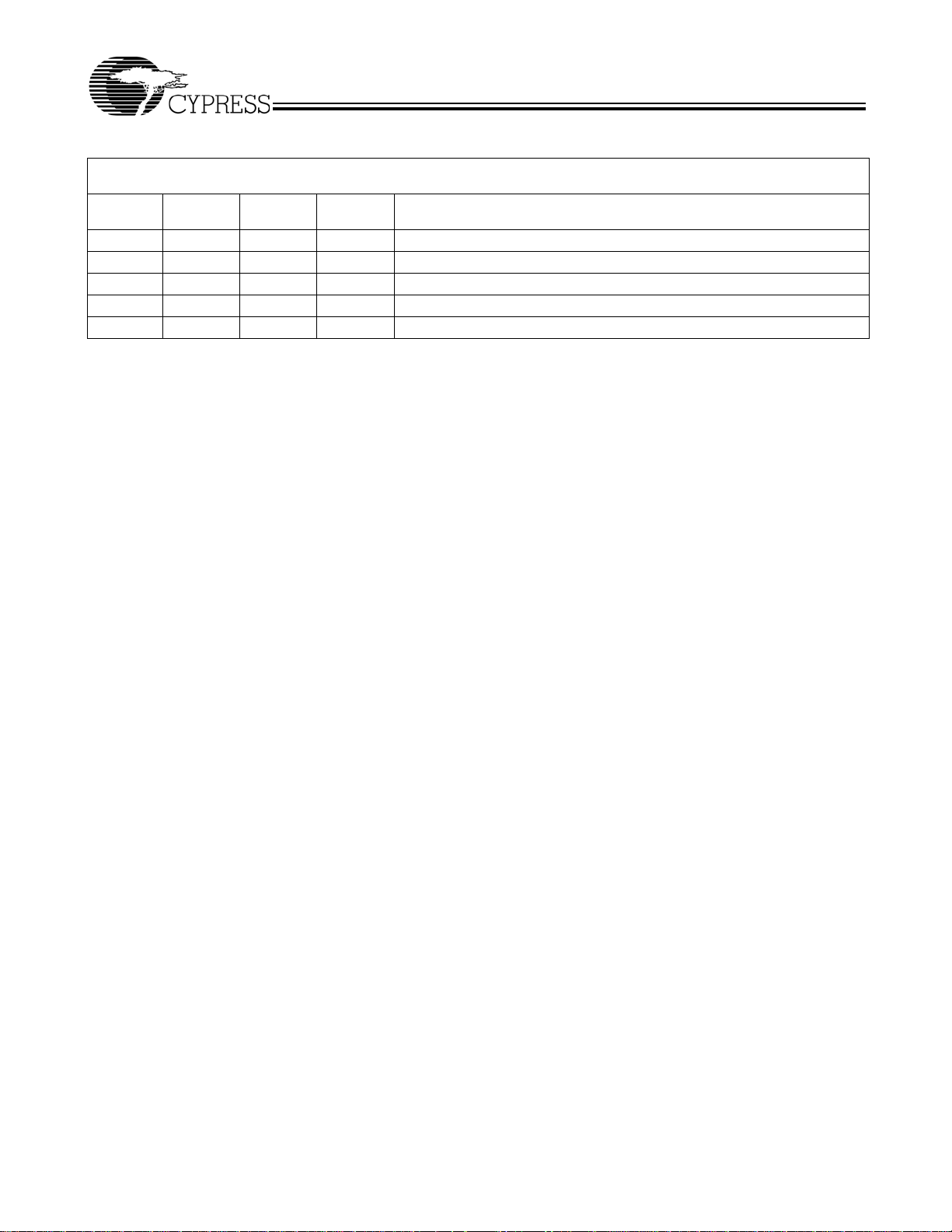
Part Number Outputs Input Frequency Range Output Frequency Range Specifications
CY22050FC 6 8 MHz–30 MHz (external crystal)
1 MHz–133 MHz (driven clock)
CY22050FI 6 8 MHz–30 MHz (external crystal)
1 MHz–133 MHz (driven clock)
Logic Block Diagram
XIN
XOUT
OE
Pin Configuration
OSC.
Q
Φ
P
AVDD
AVDD
PWRDWN
LCLK1
LCLK2
VCO
PLL
AVSS
XIN
VDD
AVSS
VSSL
VSS
1
2
3
4
5
6
7
8
80 kHz–200 MHz (3.3V)
80 KHz–166.6 MHz (2.5V)
80 kHz–166.6 MHz (3.3V)
80 KHz–150 MHz (2.5V)
Divider
Bank 1
Divider
Bank 2
VDDL
VSSLVDD
PWRDWN
XOUT
16
15
CLK6
14
CLK5
13
VSS
12
LCLK4
11
VDDL
10
OE
9
LCLK3
Field-programmable
commercial temperature
Field-programmable
industrial temperature
Output
Select
Matrix
LCLK1
LCLK2
LCLK3
LCLK4
CLK5
CLK6
Cypress Semiconductor Corporation • 3901 North First Street • San Jose, CA 95134 • 408-943-2600
Document #: 38-07006 Rev. *D Revised January 29, 2005
CY22050 Pin Summary
Name Pin Number Description
XIN 1 Reference Input. Driven by a crystal (8 MHz–30 MHz) or external clock (1 MHz–133 MHz).
Programmable input load capacitors allow for maximum flexibility in selecting a crystal, based
on manufacturer, process, performance, or quality.
VDD 2 3.3V voltage supply
AVD D 3 3.3V analog voltage supply
PWRDWN
LCLK1 7 Configurable clock output 1 at V
LCLK2 8 Configurable clock output 2 at V
LCLK3 9 Configurable clock output 3 at V
LCLK4 12 Configurable clock output 4 at V
XOUT
[1]
4 Power Down. When pin 4 is driven LOW, the CY22050 will go into shut-down mode.
AVSS 5 Analog ground
VSSL 6 LCLK ground
DDL
DDL
DDL
OE
[1]
10 Output Enable. When pin 10 is driven LOW, all outputs are three-stated.
VDDL 11 LCLK voltage supply (2.5V or 3.3V)
DDL
VSS 13 Ground
CLK5 14 Configurable clock output 5 (3.3V)
CLK6 15 Configurable clock output 6 (3.3V)
[2]
16 Reference output
level (3.3V or 2.5V)
level (3.3V or 2.5V)
level (3.3V or 2.5V)
level (3.3V or 2.5V)
CY22050
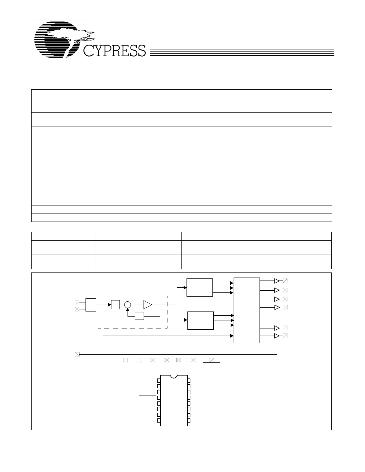
Functional Description
The CY22050 is the next-generation programmable FTG
(frequency timing generator) for use in networking, telecommunication, datacom, and other general-purpose applications.
The CY22050 offers up to six configurable outputs in a 16-pin
TSSOP, running off a 3.3V power supply. The on-chip
reference oscillator is designed to run off an 8–30-MHz crystal,
or a 1–133-MHz external clock signal.
The CY22050 has a single PLL driving 6 programmable output
clocks. The output clocks are derived from the PLL or the
reference frequency (REF). Output post dividers are available
for either. Four of the outputs can be set as 3.3V or 2.5V, for
use in a wide variety of portable and low-power applications.
Field Programming the CY22050F
The CY22050 is programmed at the package level, i.e., in a
programmer socket. The CY22050 is flash-technology based,
so the parts can be reprogrammed up to 100 times. This allows
for fast and easy design changes and product updates, and
eliminates any issues with old and out-of-date inventory.
Samples and small prototype quantities can be programmed
on the CY3672 programmer. Cypress’s value-added distribution partners and third-party programming systems from BP
Microsystems, HiLo Systems, and others are available for
large-production quantities.
CyClocksRT Software
CyClocksRT™ is an easy-to-use software application that
allows the user to custom-configure the CY22050. Users can
specify the REF, PLL frequency, output frequencies and/or
post-dividers, and different functional options. CyClocksRT
outputs an industry-standard JEDEC file used for
programming the CY22050.
CyClocksRT can be downloaded free of charge from the
Cypress website at http://www.cypress.com.
CY3672 FTG Development Kit
The Cypress CY3672 FTG Development Kit comes complete
with everything needed to design with the CY22050 and
program samples and small prototype quantities. The kit
comes with the latest version of CyClocksRT and a small
portable programmer that connects to a PC serial port for
on-the-fly programming of custom frequencies.
The JEDEC file output of CyClocksRT can be downloaded to
the portable programmer for small-volume programming, or
for use with a production programming system for larger
volumes.
Applications
Controlling Jitter
Jitter is defined in many ways, including: phase noise,
long-term jitter, cycle-to-cycle jitter, period jitter, absolute jitter,
and deterministic jitter. These jitter terms are usually given in
terms of rms, peak-to-peak, or in the case of phase noise
dBC/Hz with respect to the fundamental frequency. Actual
jitter is dependent on XIN jitter and edge rate, number of active
outputs, output frequencies, V
and output load.
Power supply noise and clock output loading are two major
system sources of clock jitter. Power supply noise can be
mitigated by proper power supply decoupling (0.1-µF ceramic
cap) of the clock and ensuring a low-impedance ground to the
(2.5V or 3.3V), temperature,
DDL
Notes:
1. The CY22050 has no internal pull-up or pull-down resistors. PWRDWN
2. Float XOUT if XIN is driven by an external clock source.
and OE pins need to be driven as appropriate or tied to power or ground.
Document #: 38-07006 Rev. *D Page 2 of 9
CY22050
chip. Reducing capacitive clock output loading to a minimum
lowers current spikes on the clock edges and thus reduces
jitter.
Reducing the total number of active outputs will also reduce
jitter in a linear fashion. However, it is better to use two outputs
to drive two loads than one output to drive two loads.
The rate and magnitude that the PLL corrects the VCO
frequency is directly related to jitter performance. If the rate is
too slow, then long term jitter and phase noise will be poor.
Therefore, to improve long-term jitter and phase noise,
reducing Q to a minimum is advisable. This technique will
increase the speed of the phase frequency detector, which in
turn drives the input voltage of the VCO. In a similar manner,
increasing P until the VCO is near its maximum rated speed
will also decrease long term jitter and phase noise. For
example: input reference of 12 MHz; desired output frequency
of 33.3 MHz. One might arrive at the following solution: Set
Q = 3, P = 25, Post Div = 3. However, the best jitter results will
be Q = 2, P = 50, Post Div = 9.
For additional information, refer to the application note, “Jitter
in PLL-based Systems: Causes, Effects, and Solutions,”
available at http://www.cypress.com (click on “Application
Notes”), or contact your local Cypress Field Applications
Engineer.
CY22050 Frequency Calculation
The CY22050 is an extremely flexible clock generator with up
to six individual outputs, generated from an integrated PLL.
There are four variables used to determine the final output
frequency. They are: the input REF, the P and Q dividers, and
the post divider. The three basic formulas for determining the
final output frequency of a CY22150-based design are:
• CLK = ((REF * P)/Q)/Post Divider
• CLK = REF/Post Divider
•CLK = REF
The basic PLL block diagram is shown in Figure 1. Each of the
six clock outputs has a total of seven output options available
to it. There are six post divider options: /2 (two of these), /3, /4,
/DIV1N, and DIV2N. DIV1N and DIV2N are separately calculated and can be independent of each other. The post divider
options can be applied to the calculated PLL frequency or to
the REF directly.
In addition to the six post divider options, the seventh option
bypasses the PLL and passes the REF directly to the crosspoint switch matrix.
Clock Output Settings: Crosspoint Switch
Matrix
Each of the six clock outputs can come from any of seven
unique frequency sources. The crosspoint switch matrix
defines which source is attached to each individual clock
output. Although it may seem that there are an unlimited
number of divider options, there are several rules that should
be taken into account when selecting divider options.
Divider Bank 1
/DIV1N
REF
Q
PFD
VCO
/2
/3
P
Divider Bank 2
/4
/2
/DIV2N
Figure 1. Basic PLL Block Diagram
Clock Output Divider Definition and Notes
None Clock output source is the reference input frequency
/DIV1N Clock output uses a generated /DIV1N option from Divider Bank 1. Allowable values for DIV1N are
4 to 127. If Divider Bank 1 is not being used, set DIV1N to 8.
/2 Clock output uses a fixed /2 option from Divider Bank 1. If this option is used, DIV1N must be divisible
by 4.
/3 Clock output uses a fixed /3 option from Divider Bank 1. If this option is used, set DIV1N to 6.
/DIV2N Clock output uses a generated /DIV2N option from Divider Bank 2. Allowable values for DIV2N are
/2 Clock output uses a fixed /2 option from Divider Bank 2. If this option is used, DIV2N must be divisible
/4 Clock output 2 uses a fixed /4 option from Divider Bank 2. If this option is used, DIV2N must be
4 to 127. If Divider Bank 2 is not being used, set DIV2N to 8.
by 4.
divisible by 8.
Crosspoint
Switch
Matrix
LCLK1
LCLK2
LCLK3
LCLK4
CLK5
CLK6
Document #: 38-07006 Rev. *D Page 3 of 9
CY22050
Reference Crystal Input
The input crystal oscillator of the CY22050 is an important
feature because of the flexibility it allows the user in selecting
a crystal as a reference clock source. The oscillator inverter
has programmable gain, allowing for maximum compatibility
with a reference crystal, based on manufacturer, process,
performance, and quality.
The value of the input load capacitors is determined by eight
bits in a programmable register. Total load capacitance is
determined by the formula:
CapLoad = (C
– C
L
BRD
– C
)/0.09375 pF
CHIP
In CyClocksRT, enter the crystal capacitance (C
of CapLoad will be determined automatically and programmed
into the CY22050.
If you require greater control over the CapLoad value, consider
using the CY22150F for serial configuration and control of the
input load capacitors. For an external clock source, the default
is 0.
Input load capacitors are placed on the CY22050 die to reduce
external component cost. These capacitors are true
parallel-plate capacitors, designed to reduce the frequency
shift that occurs when non-linear load capacitance is affected
by load, bias, supply, and temperature changes.
). The value
L
Absolute Maximum Conditions
Parameter Description Min. Max. Unit
V
DD
V
DDL
T
S
T
J
ESD Static Discharge Voltage per MIL-STD-833, Method 3015 2000 V
Supply Voltage –0.5 7.0 V
I/O Supply Voltage –0.5 7.0 V
Storage Temperature
[3]
–65 125 °C
Junction Temperature 125 °C
Package Power Dissipation—Commercial Temp 450 mW
Package Power Dissipation—Industrial Temp 380 mW
Digital Inputs AV
Digital Outputs referred to V
Digital Outputs referred to V
DD
DDL
– 0.3 AV
SS
+ 0.3 V
DD
VSS – 0.3 VDD + 0.3 V
VSS – 0.3 V
+0.3 V
DDL
Recommended Operating Conditions
Parameter Description Min. Typ. Max. Unit
V
DD
VDDL
HI
VDDL
LO
T
AC
T
AI
C
LOAD
C
LOAD
f
REFD
f
REFC
t
PU
Note:
3. Rated for 10 years.
Operating Voltage 3.135 3.3 3.465 V
Operating Voltage 3.135 3.3 3.465 V
Operating Voltage 2.375 2.5 2.625 V
Ambient Commercial Temp 0 70 °C
Ambient Industrial Temp –40 85 °C
Max. Load Capacitance VDD/V
Max. Load Capacitance V
DDL
= 3.3V 15 pF
DDL
= 2.5V 15 pF
Driven REF 1 133 MHz
Crystal REF 8 30 MHz
Power-up time for all VDDs to reach minimum
0.05 500 ms
specified voltage (power ramps must be
monotonic)
Document #: 38-07006 Rev. *D Page 4 of 9

CY22050
DC Electrical Characteristics
Parameter
I
OH3.3
I
OL3.3
I
OH2.5
I
OL2.5
V
IH
V
IL
[5,6]
I
VDD
I
VDDL3.3
I
VDDL2.5
I
DDS
I
OHZ
I
OLZ
AC Electrical Characteristics
Parameter
Notes:
4. Not 100% tested, guaranteed by design.
5. I
VDD
6. Use CyClocksRT to calculate actual I
7. Skew value guaranteed when outputs are generated from the same divider bank. See Logic Block Diagram for more information.
8. Jitter measurement will vary. Actual jitter is dependent on XIN jitter and edge rate, number of active outputs, output frequencies, V
and output load. For more information, refer to the application note, “Jitter in PLL-based Systems: Causes, Effects, and Solutions,” available at http://www.cypress.com, or contact your local Cypress Field Applications Engineer.
[4]
Output High Current VOH = VDD – 0.5V, VDD/V
Output Low Current VOL = 0.5V, VDD/V
Output High Current VOH = V
Output Low Current VOL = 0.5V, V
Input High Voltage CMOS levels, 70% of V
Input Low Voltage CMOS levels, 30% of V
Name Description Min. Typ. Max. Unit
= 3.3V 12 24 mA
DDL
= 3.3V 12 24 mA
DDL
– 0.5V, V
DDL
= 2.5V 8 16 mA
DDL
= 2.5V 8 16 mA
DDL
DD
DD
0.7 1.0 V
00.3V
Supply Current AVDD/VDD Current 45 mA
[5,6]
[5,6]
t1 Output frequency,
t2 Output duty cycle Duty cycle is defined in Figure 2; t1/t2
t3
LO
t4
LO
t3
HI
t4
HI
[7]
t5
[8]
t6
Supply Current V
Supply Current V
Power-Down Current V
Output Leakage V
[4]
Name Description Min. Typ. Max. Unit
Current (V
DDL
Current (V
DDL
= V
DD
= V
DD
DDL
DDL
= AV
= AV
= 3.465V) 25 mA
DDL
= 2.625V) 17 mA
DDL
= 3.465V 50 µA
DD
= 3.465V 10 µA
DD
Clock output limit, 3.3V 0.08 (80 kHz) 200 MHz
commercial temp
Output frequency,
industrial temp
Clock output limit, 2.5V 0.08 (80 kHz) 166.6 MHz
Clock output limit, 3.3V 0.08 (80 kHz) 166.6 MHz
Clock output limit, 2.5V 0.08 (80 kHz) 150 MHz
40 50 60 %
f
> 166 MHz, 50% of V
Rising edge slew
DDL
= 2.5V)
rate (V
Falling edge slew
DDL
= 2.5V)
rate (V
Rising edge slew
DDL
= 3.3V)
rate (V
Falling edge slew
DDL
= 3.3V)
rate (V
OUT
Duty cycle is defined in Figure 2; t1/t2
< 166 MHz, 50% of V
f
OUT
Output clock rise time, 20% – 80% of V
Defined in Figure 3
Output clock fall time, 80% – 20% of V
Defined in Figure 3
Output clock rise time, 20% – 80% of
VDD/V
. Defined in Figure 3
DDL
Output clock fall time, 80% – 20% of
VDD/V
. Defined in Figure 3
DDL
DD
DD
DDL
DDL
45 50 55 %
.
.
0.6 1.2 V/ns
0.6 1.2 V/ns
0.8 1.4 V/ns
0.8 1.4 V/ns
Skew Output-output skew between related outputs 250 ps
Clock jitter Peak-to-peak period jitter (see Figure 4)250ps
t10 PLL lock time 0.30 3 ms
currents specified for two CLK outputs running at 125 MHz, two LCLK outputs running at 80 MHz, and two LCLK outputs running at 66.6 MHz.
VDD
and I
for specific output frequency configurations.
VDDL
(2.5V or 3.3V), temperature,
DDL
DD
DD
Document #: 38-07006 Rev. *D Page 5 of 9

Test Circuit
V
DD
0.1 µF
OUTPUTS
CLK out
C
LOAD
CY22050
AV
DD
0.1 µF
CLK
GND
t1
t2
50%
Figure 2. Duty Cycle Definition: DC = t2/t1
t3
80%
CLK
Figure 3. Rise and Fall Time Definitions
20%
t6
50%
t4
V
DDL
0.1 µF
CLK
Figure 4. Peak-to-Peak Jitter
Document #: 38-07006 Rev. *D Page 6 of 9

CY22050
Ordering Information
Ordering Code Package Type
Range
CY22050FC 16-lead TSSOP Commercial (0 to 70°C) 3.3V
CY22050FI 16-lead TSSOP Industrial (–40 to 85°C) 3.3V
Temperature Operating
[9]
[9]
[9]
16-lead TSSOP Commercial (0 to 70°C) 3.3V
16-lead TSSOP-Tape and Reel Commercial (0 to 70°C) 3.3V
16-lead TSSOP Industrial (–40 to 85°C) 3.3V
[9]
16-lead TSSOP-Tape and Reel Industrial (–40 to 85°C) 3.3V
CY22050ZC-xxx
CY22050ZC-xxxT
CY22050ZI-xxx
CY22050ZI-xxxT
CY3672 FTG Development Kit
CY3672ADP000 CY22050F Socket
Lead-free
CY22050FZXC 16-lead TSSOP Commercial (0 to 70°C) 3.3V
CY22050FZXI 16-lead TSSOP Industrial (–40 to 85°C) 3.3V
CY22050ZXC-xxx
CY22050ZXC-xxxT
CY22050ZXI-xxx
CY22050ZXI-xxxT
[9]
[9]
[9]
[9]
16-lead TSSOP Commercial (0 to 70°C) 3.3V
16-lead TSSOP-Tape and Reel Commercial (0 to 70°C) 3.3V
16-lead TSSOP Industrial (–40 to 85°C) 3.3V
16-lead TSSOP-Tape and Reel Industrial (–40 to 85°C) 3.3V
Operating
Vol tag e
16-lead TSSOP Package Characteristics
Parameter Name Value Unit
θ
JA
Complexity Transistor Count 74,600 Transistors
Note:
9. The CY22050ZC-xxx and CY22050ZI-xxx are factory-programmed configurations. Factory programming is available for high-volume design opportunities of
100 Ku/year or more in production. For more details, contact your local Cypress field application engineer or Cypress sales representative.
theta JA 115 °C/W
Document #: 38-07006 Rev. *D Page 7 of 9

Package Drawing and Dimensions
16-lead TSSOP 4.40 MM Body Z16.173
CY22050
1
PIN1ID
DIMENSIONS IN MM[INCHES] MIN.
MAX.
REFERENCE JEDEC MO-153
0.65[0.025]
0.85[0.033]
0.95[0.037]
BSC.
4.90[0.193]
5.10[0.200]
4.30[0.169]
4.50[0.177]
16
0.19[0.007]
0.30[0.012]
0.05[0.002]
0.15[0.006]
6.25[0.246]
6.50[0.256]
1.10[0.043] MAX.
0.076[0.003]
SEATING
PLANE
PACKAGE WEIGHT 0.05gms
0.25[0.010]
BSC
GAUGE
PLANE
0°-8°
0.50[0.020]
0.70[0.027]
51-85091-*A
0.09[[0.003]
0.20[0.008]
CyClocksRT is a trademark of Cypress Semiconductor Corporation. BP Microsystems is a trademark of BP Microsystems. Hilo
Systems is a trademark of Hi-Lo Systems. All product and company names mentioned in this document are the trademarks of
their respective holders.
Document #: 38-07006 Rev. *D Page 8 of 9
© Cypress Semiconductor Corporation, 2005. The information contained herein is subject to change without notice. Cypress Semiconductor Corporation assumes no responsibility for the use
of any circuitry other than circuitry embodied in a Cypress product. Nor does it convey or imply any license under patent or other rights. Cypress products are not warranted nor intended to be
used for medical, life support, life saving, critical control or safety applications, unless pursuant to an express written agreement with Cypress. Furthermore, Cypress does not authorize its
products for use as critical components in life-support systems where a malfunction or failure may reasonably be expected to result in significant injury to the user. The inclusion of Cypress
products in life-support systems application implies that the manufacturer assumes all risk of such use and in doing so indemnifies Cypress against all charges.
Document History Page
Document Title: CY22050 One-PLL General Purpose Flash-Programmable Clock Generator
Document Number: 38-07006
REV. ECN NO.
** 108185 08/08/01 CKN New Data Sheet
*A 110054 03/04/02 CKN Changed from Preliminary to Final
*B 121862 12/14/02 RBI Power up requirements added to Operating Conditions Information
*C 310575 See ECN RGL Added Lead-free devices
*D 314233 See ECN RGL Removed the Tape and Reel devices in the non-dash parts
Issue
Date
Orig. of
Change Description of Change
CY22050
Document #: 38-07006 Rev. *D Page 9 of 9
 Loading...