

CTLST CAT24WC64PI-TE13, CAT24WC64PI-1.8TE13, CAT24WC64PA-1.8TE13, CAT24WC64P-TE13, CAT24WC64P-1.8TE13 Datasheet
...
1
D
OUT
ACK
SENSE AMPS
SHIFT REGISTERS
CONTROL
LOGIC
WORD ADDRESS
BUFFERS
STAR T/STOP
LOGIC
STATE COUNTERS
SLAVE
ADDRESS
COMPARATORS
E2PROM
128/256 X 256
V
CC
EXTERNAL LOAD
COLUMN
DECODERS
XDEC
DATA IN STORAGE
HIGH VOL TAGE/
TIMING CONTROL
V
SS
WP
SCL
A
0
A1
A2
SDA
128/256
256
V
CC
WP
SCL
SDA
1
2
3
4
8
7
6
5
A
0
V
CC
WP
SCL
SDA
1
2
3
4
8
7
6
5
A
1
A
2
V
SS
A
0
A
1
A
2
V
SS
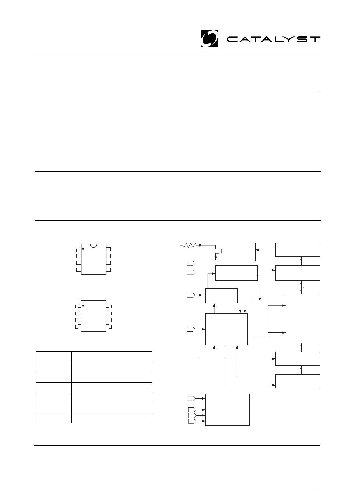
DESCRIPTION
The CAT24WC32/64 is a 32K/64K-bit Serial CMOS
E2PROM internally organized as 4096/8192 words of 8
bits each. Catalyst’s advanced CMOS technology substantially reduces device power requirements. The
Preliminary
* Catalyst Semiconductor is licensed by Philips Corporation to carry the I2C Bus Protocol.
■ Zero Standby Current
■ Commercial, Industrial and Automotive
Temperature Ranges
■ Write Protection
– Entire Array Protected When WP at V
IH
■ 1,000,000 Program/Erase Cycles
■ 100 Year Data Retention
CAT24WC32/64 features a 32-byte page write buffer.
The device operates via the I2C bus serial interface and
is available in 8-pin DIP or 8-pin SOIC packages.
PIN CONFIGURATION BLOCK DIAGRAM
PIN FUNCTIONS
Pin Name Function
A0, A1, A2 Device Address Inputs
SDA Serial Data/Address
SCL Serial Clock
WP Write Protect
V
CC
+1.8V to +6V Power Supply
V
SS
Ground
24WC32/64 F02
CAT24WC32/64
32K/64K-Bit I2C Serial CMOS E2PROM
■ 400 KHz I
2
C Bus Compatible*
■ 1.8 to 6 Volt Read and Write Operation
■ Cascadable for up to Eight Devices
■ 32-Byte Page Write Buffer
■ Self-Timed Write Cycle with Auto-Clear
■ 8-Pin DIP or 8-Pin SOIC
■ Schmitt Trigger Inputs for Noise Protection
FEATURES
DIP Package (P)
SOIC Package (J,K)
24WC32/64 F01
© 1998 by Catalyst Semiconductor, Inc.
Characteristics subject to change without notice
Doc. No. 25053-00 2/98 S-1
PreliminaryCAT24WC32/64
2
Doc. No. 25053-00 2/98 S-1
ABSOLUTE MAXIMUM RATINGS*
Temperature Under Bias ................. –55°C to +125°C
Storage Temperature....................... –65°C to +150°C
Voltage on Any Pin with
Respect to Ground
(1)
........... –2.0V to +V
CC
+ 2.0V
VCC with Respect to Ground ............... –2.0V to +7.0V
Package Power Dissipation
Capability (Ta = 25°C)................................... 1.0W
Lead Soldering Temperature (10 secs) ............ 300°C
Output Short Circuit Current
(2)
........................ 100mA
*COMMENT
Stresses above those listed under “Absolute Maximum
Ratings” may cause permanent damage to the device.
These are stress ratings only, and functional operation of
the device at these or any other conditions outside of those
listed in the operational sections of this specification is not
implied. Exposure to any absolute maximum rating for
extended periods may affect device performance and
reliability.
RELIABILITY CHARACTERISTICS
Symbol Parameter Min. Max. Units Reference Test Method
N
END
(3)
Endurance 1,000,000 Cycles/Byte MIL-STD-883, Test Method 1033
T
DR
(3)
Data Retention 100 Years MIL-STD-883, Test Method 1008
V
ZAP
(3)
ESD Susceptibility 2000 Volts MIL-STD-883, Test Method 3015
I
LTH
(3)(4)
Latch-up 100 mA JEDEC Standard 17
Limits
Symbol Parameter Min. Typ. Max. Units Test Conditions
I
CC
Power Supply Current 3 mA f
SCL
= 100 KHz
I
SB
(5)
Standby Current (VCC = 5V) 0 µAVIN = GND or V
CC
I
LI
Input Leakage Current 10 µAVIN = GND to V
CC
I
LO
Output Leakage Current 10 µAV
OUT
= GND to V
CC
V
IL
Input Low Voltage –1 VCC x 0.3 V
V
IH
Input High Voltage VCC x 0.7 VCC + 0.5 V
V
OL1
Output Low Voltage (VCC = +3.0V) 0.4 V IOL = 3.0 mA
V
OL2
Output Low Voltage (VCC = +1.8V) 0.5 V IOL = 1.5 mA
D.C. OPERATING CHARACTERISTICS
VCC = +1.8V to +6.0V, unless otherwise specified.
CAPACITANCE TA = 25°C, f = 1.0 MHz, VCC = 5V
Symbol Test Max. Units Conditions
C
I/O
(3)
Input/Output Capacitance (SDA) 8 pF V
I/O
= 0V
C
IN
(3)
Input Capacitance (A0, A1, A2, SCL, WP) 6 pF V
IN
= 0V
Note:
(1) The minimum DC input voltage is –0.5V. During transitions, inputs may undershoot to –2.0V for periods of less than 20 ns. Maximum DC
voltage on output pins is VCC +0.5V, which may overshoot to VCC + 2.0V for periods of less than 20ns.
(2) Output shorted for no more than one second. No more than one output shorted at a time.
(3) This parameter is tested initially and after a design or process change that affects the parameter.
(4) Latch-up protection is provided for stresses up to 100 mA on address and data pins from –1V to VCC +1V.
(5) Standby current (ISB ) = 0 µA (<900 nA).
Preliminary CAT24WC32/64
3
Doc. No. 25053-00 2/98 S-1
The write cycle time is the time from a valid stop
condition of a write sequence to the end of the internal
program/erase cycle. During the write cycle, the bus
interface circuits are disabled, SDA is allowed to remain
high, and the device does not respond to its slave
address.
A.C. CHARACTERISTICS
VCC = +1.8V to +6V, unless otherwise specified
Output Load is 1 TTL Gate and 100pF
Read & Write Cycle Limits
Symbol Parameter 1.8V, 2.5 V 4.5V-5.5V
Min. Max. Min. Max. Units
F
SCL
Clock Frequency 100 400 kHz
T
I
(1)
Noise Suppression Time 200 200 ns
Constant at SCL, SDA Inputs
t
AA
SCL Low to SDA Data Out 3.5 1 µs
and ACK Out
t
BUF
(1)
Time the Bus Must be Free Before 4.7 1.2 µs
a New Transmission Can Start
t
HD:STA
Start Condition Hold Time 4 0.6 µs
t
LOW
Clock Low Period 4.7 1.2 µs
t
HIGH
Clock High Period 4 0.6 µs
t
SU:STA
Start Condition Setup Time 4.7 0.6 µs
(for a Repeated Start Condition)
t
HD:DAT
Data In Hold Time 0 0 ns
t
SU:DAT
Data In Setup Time 50 50 ns
t
R
(1)
SDA and SCL Rise Time 1 0.3 µs
t
F
(1)
SDA and SCL Fall Time 300 300 ns
t
SU:STO
Stop Condition Setup Time 4 0.6 µs
t
DH
Data Out Hold Time 100 100 ns
Power-Up Timing
(1)(2)
Symbol Parameter Max. Units
t
PUR
Power-Up to Read Operation 1 ms
t
PUW
Power-Up to Write Operation 1 ms
Note:
(1) This parameter is tested initially and after a design or process change that affects the parameter.
(2) t
PUR
and t
PUW
are the delays required from the time VCC is stable until the specified operation can be initiated.
Write Cycle Limits
Symbol Parameter Min. Typ. Max Units
t
WR
Write Cycle Time 10 ms

PreliminaryCAT24WC32/64
4
Doc. No. 25053-00 2/98 S-1
FUNCTIONAL DESCRIPTION
The CAT24WC32/64 supports the I2C Bus data transmission protocol. This Inter-Integrated Circuit Bus protocol defines any device that sends data to the bus to be
a transmitter and any device receiving data to be a
receiver. The transfer is controlled by the Master device
which generates the serial clock and all START and
STOP conditions for bus access. The CAT24WC32/64
operates as a Slave device. Both the Master device and
Slave device can operate as either transmitter or receiver, but the Master device controls which mode is
activated.
PIN DESCRIPTIONS
SCL: Serial Clock
The serial clock input clocks all data transferred into or
out of the device.
SDA: Serial Data/Address
The bidirectional serial data/address pin is used to
transfer all data into and out of the device. The SDA pin
is an open drain output and can be wire-ORed with other
open drain or open collector outputs.
A0, A1, A2: Device Address Inputs
These pins are hardwired or left unconnected (for hardware compatibility with CAT24WC16). When hardwired,
up to eight CAT24WC32/64s may be addressed on a
single bus system (refer to Device Addressing ). When
the pins are left unconnected, the default values are
zeros.
WP: Write Protect
This input, when tied to GND, allows write operations to
the entire memory. For CAT24WC32/64 when this pin
is tied to Vcc, the entire memory is write protected.
When left floating, memory is unprotected.
5020 FHD F05
Figure 3. Start/Stop Timing
Figure 2. Write Cycle Timing
Figure 1. Bus Timing
START BIT
SDA
STOP BIT
SCL
5020 FHD F04
t
WR
STOP
CONDITION
START
CONDITION
ADDRESS
ACK8TH BIT
BYTE n
SCL
SDA
5020 FHD F03
t
HIGH
SCL
SDA IN
SDA OUT
t
LOW
t
F
t
LOW
t
R
t
BUF
t
SU:STO
t
SU:DAT
t
HD:DAT
t
HD:STA
t
SU:STA
t
AA
t
DH

Preliminary CAT24WC32/64
5
Doc. No. 25053-00 2/98 S-1
I2C BUS PROTOCOL
The features of the I2C bus protocol are defined as
follows:
(1) Data transfer may be initiated only when the bus is
not busy.
(2) During a data transfer, the data line must remain
stable whenever the clock line is high. Any changes
in the data line while the clock line is high will be
interpreted as a START or STOP condition.
START Condition
The START Condition precedes all commands to the
device, and is defined as a HIGH to LOW transition of
SDA when SCL is HIGH. The CAT24WC32/64 monitors
the SDA and SCL lines and will not respond until this
condition is met.
STOP Condition
A LOW to HIGH transition of SDA when SCL is HIGH
determines the STOP condition. All operations must end
with a STOP condition.
DEVICE ADDRESSING
The bus Master begins a transmission by sending a
START condition. The Master sends the address of the
particular slave device it is requesting. The four most
significant bits of the 8-bit slave address are fixed as
1010 (Fig. 5). The next three bits (A2, A1, A0) are the
device address bits; up to eight 32K/64K devices may
to be connected to the same bus. These bits must
Figure 4. Acknowledge Timing
5027 FHD F07
Figure 5. Slave Address Bits
5020 FHD F06
ACKNOWLEDGE
1
START
SCL FROM
MASTER
89
DATA OUTPUT
FROM TRANSMITTER
DATA OUTPUT
FROM RECEIVER
1 0 1 0 A2 A1 A0 R/W
compare to the hardwired input pins, A2, A1 and A0. The
last bit of the slave address specifies whether a Read or
Write operation is to be performed. When this bit is set
to 1, a Read operation is selected, and when set to 0, a
Write operation is selected.
After the Master sends a START condition and the slave
address byte, the CAT24WC32/64 monitors the bus and
responds with an acknowledge (on the SDA line) when
its address matches the transmitted slave address. The
CAT24WC32/64 then performs a Read or Write operation depending on the state of the R/W bit.
Acknowledge
After a successful data transfer, each receiving device is
required to generate an acknowledge. The Acknowledging device pulls down the SDA line during the ninth clock
cycle, signaling that it received the 8 bits of data.
The CAT24WC32/64 responds with an acknowledge
after receiving a START condition and its slave address.
If the device has been selected along with a write
operation, it responds with an acknowledge after receiving each 8-bit byte.
When the CAT24WC32/64 begins a READ mode it
transmits 8 bits of data, releases the SDA line, and
monitors the line for an acknowledge. Once it receives
this acknowledge, the CAT24WC32/64 will continue to
transmit data. If no acknowledge is sent by the Master,
the device terminates data transmission and waits for a
STOP condition. The master must then issue a stop
condition to return the CAT24WC32/64 to the standby
power mode and place the device in a known state.

PreliminaryCAT24WC32/64
6
Doc. No. 25053-00 2/98 S-1
A15–A
8
SLAVE
ADDRESS
S
A
C
K
A
C
K
A
C
K
BUS ACTIVITY :
MASTER
SDA LINE
S
T
A
R
T
A7–A
0
BYTE ADDRESS
DATA n+31DATA
A
C
K
S
T
O
P
A
C
K
DATA n
A
C
K
P
A
C
K
*
XXX
A15–A
8
SLAVE
ADDRESS
S
A
C
K
A
C
K
DATA
A
C
K
S
T
O
P
P
BUS ACTIVITY :
MASTER
SDA LINE
S
T
A
R
T
A7–A
0
BYTE ADDRESS
A
C
K
*
XXX
WRITE OPERATIONS
Byte Write
In the Byte Write mode, the Master device sends the
START condition and the slave address information
(with the R/W bit set to zero) to the Slave device. After
the Slave generates an acknowledge, the Master sends
two 8-bit address words that are to be written into the
address pointers of the CAT24WC32/64. After receiving
another acknowledge from the Slave, the Master device
transmits the data to be written into the addressed
memory location. The CAT24WC32/64 acknowledges
once more and the Master generates the STOP condition. At this time, the device begins an internal programming cycle to nonvolatile memory. While the cycle is in
progress, the device will not respond to any request from
the Master device.
Page Write
The CAT24WC32/64 writes up to 32 bytes of data, in a
single write cycle, using the Page Write operation. The
page write operation is initiated in the same manner as
the byte write operation, however instead of terminating
after the initial byte is transmitted, the Master is allowed
to send up to 31 additional bytes. After each byte has
been transmitted, CAT24WC32/64 will respond with an
acknowledge, and internally increment the five low order
address bits by one. The high order bits remain unchanged.
If the Master transmits more than 32 bytes before sending
the STOP condition, the address counter ‘wraps around’,
and previously transmitted data will be overwritten.
When all 32 bytes are received, and the STOP condition
has been sent by the Master, the internal programming
cycle begins. At this point, all received data is written to
the CAT24WC32/64 in a single write cycle.
Acknowledge Polling
Disabling of the inputs can be used to take advantage of
the typical write cycle time. Once the stop condition is
issued to indicate the end of the host's write operation,
CAT24WC32/64 initiates the internal write cycle. ACK
polling can be initiated immediately. This involves issuing the start condition followed by the slave address for
a write operation. If CAT24WC32/64 is still busy with the
write operation, no ACK will be returned. If
CAT24WC32/64 has completed the write operation, an
ACK will be returned and the host can then proceed with
the next read or write operation.
WRITE PROTECTION
The Write Protection feature allows the user to protect
against inadvertent programming of the memory array.
If the WP pin is tied to VCC, the entire memory array is
protected and becomes read only. The CAT24WC32/64
will accept both slave and byte addresses, but the
24WC32/64 F09
Figure 7. Page Write Timing
Figure 6. Byte Write Timing
24WC32/64 F08
* = Don't care bit for 24WC32
X= Don't care bit

Preliminary CAT24WC32/64
7
Doc. No. 25053-00 2/98 S-1
memory location accessed is protected from programming by the device’s failure to send an acknowledge
after the first byte of data is received.
READ OPERATIONS
The READ operation for the CAT24WC32/64 is initiated
in the same manner as the write operation with one
exception, that R/W bit is set to one. Three different
READ operations are possible: Immediate/Current Address READ, Selective/Random READ and Sequential
READ.
Immediate/Current Address Read
The CAT24WC32/64’s address counter contains the
address of the last byte accessed, incremented by one.
In other words, if the last READ or WRITE access was
to address N, the READ immediately following would
access data from address N+1. If N=E (where E=4095
for 24WC32 and E=8191 for 24WC64), then the counter
will ‘wrap around’ to address 0 and continue to clock out
data. After the CAT24WC32/64 receives its slave address information (with the R/W bit set to one), it issues
an acknowledge, then transmits the 8 bit byte requested.
The master device does not send an acknowledge, but
will generate a STOP condition.
Selective/Random Read
Selective/Random READ operations allow the Master
device to select at random any memory location for a
READ operation. The Master device first performs a
‘dummy’ write operation by sending the START condition, slave address and byte addresses of the location it
wishes to read. After CAT24WC32/64 acknowledges,
the Master device sends the START condition and the
slave address again, this time with the R/W bit set to one.
The CAT24WC32/64 then responds with its acknowledge and sends the 8-bit byte requested. The master
device does not send an acknowledge but will generate
a STOP condition.
Sequential Read
The Sequential READ operation can be initiated by
either the Immediate Address READ or Selective READ
operations. After the CAT24WC32/64 sends the initial 8bit byte requested, the Master will respond with an
acknowledge which tells the device it requires more
data. The CAT24WC32/64 will continue to output an 8bit byte for each acknowledge sent by the Master. The
operation will terminate when the Master fails to respond
with an acknowledge, thus sending the STOP condition.
The data being transmitted from CAT24WC32/64 is
outputted sequentially with data from address N followed by data from address N+1. The READ operation
address counter increments all of the CAT24WC32/64
address bits so that the entire memory array can be read
during one operation. If more than E (where E=4095 for
24WC32 and E=8191 for 24WC64) bytes are read out,
the counter will ‘wrap around’ and continue to clock out
data bytes.
Figure 8. Immediate Address Read Timing
24WC32/64 F10
SCL
SDA 8TH BIT
STOPNO ACKDATA OUT
89
SLAVE
ADDRESS
S
A
C
K
BUS ACTIVITY :
MASTER
SDA LINE
S
T
A
R
T
N
O
A
C
K
DATA
S
T
O
P
P
PreliminaryCAT24WC32/64
8
Doc. No. 25053-00 2/98 S-1
A15–A
8
SLAVE
ADDRESS
S
A
C
K
A
C
K
A
C
K
BUS ACTIVITY :
MASTER
SDA LINE
S
T
A
R
T
A7–A
0
BYTE ADDRESS SLA VE
ADDRESS
S
A
C
K
N
O
A
C
K
S
T
A
R
T
DATA
P
S
T
O
P
XXX*
Figure 9. Selective Read Timing
24WC32/64 F11
* = Don't care bit for 24WC32
X= Don't care bit
ORDERING INFORMATION
Notes:
(1) The device used in the above example is a 24WC32KI-1.8TE13 (SOIC, Industrial Temperature, 1.8 Volt to 6 Volt Operating
Voltage, Tape & Reel)
Figure 10. Sequential Read Timing
5020 FHD F12
BUS ACTIVITY:
MASTER
SDA LINE
DATA n+xDATA n
A
C
K
A
C
K
DATA n+1
A
C
K
S
T
O
P
N
O
A
C
K
DATA n+2
A
C
K
P
SLAVE
ADDRESS
Temperature Range
Blank = Commercial (0˚ - 70˚C)
I = Industrial (-40˚ - 85˚C)
A = Automotive (-40˚ - 105˚C)*
* -40˚ to +125˚C is available upon request
Prefix Device # Suffix
24WC32 K
I
TE13
Product
Number
24WC32: 32K
24WC64: 64K
Tape & Reel
TE13: 2000/Reel
Package
P: PDIP
K: SOIC (EIAJ)
J: SOIC (JEDEC)
Operating Voltage
Blank: 2.5V-6.0V
1.8: 1.8V - 6.0V
-1.8CAT
Optional
Company ID
 Loading...