

Page 1

Technical Reference
MB-6862 9-Slot Dual Pentium
®
Pro
Motherboard with Natoma Chipset
Page 2

Page 3

Features
Intel Pentium
MHz and 200 MHz; and dual Pentium Pro processor
®
Pro processor, upgradeable through 180
Intel Natoma chipset
System memory upgradeable to 1 GB using x 64 or
x 72 DIMM
Processor-facilitated ECC memory with x 72 DIMM
Processor available with either 256 KB or 512 KB cache
PCI 2.1 compliant PCI/ISA bus architectures
3 ISA slots, 4 PCI slots and 1 shared PCI/ISA slots
Standard keyboard connector
On-board E-IDE controller separate master/slave IDE
mode support for up to 4 IDE drives and up to 2 floppy
drives
On-board I/O supporting 2 serial ports and 1 parallel port
On board Universal Serial Bus (USB) controller with
2 USB ports
On-board PS/2 mouse/keyboard port
On-board auxiliary serial and PS/2 mouse/keyboard ports
MB-6862
iii
Page 4

FCC Standards
The FCC (Federal Communications Commission) restricts
the amount of radiation and radio frequency emissions
coming from computing equipment.
Note: This equipment has been tested and found to comply
with the limits for a Class B digital device
pursuant to Part 15 of the FCC Rules. These limits
are designed to provide reasonable protection against harmful
interference in a residential installation. This equipment
generates, uses, and can radiate radio frequency energy and,
if not installed and used in accordance with the instructions,
may cause harmful interference to radio communications.
However, there is no guarantee that interference will not
occur in a particular installation. If this equipment does cause
harmful interference to radioor television reception, which
can be determined by turning the equipment off and on, the
use is encouraged to try to correct the interference by one
or more of the following measures:
Reorient or relocate the receiving antenna.
Increase the separation between the equipment and
receiver.
Connect the equipment into an outlet on a circuit
different from that to which the receiver is connected.
Consult the dealer or an experienced radio/TV technician
for help.
CSS Labs is not responsible for any radio or television
interference caused by unauthorized modifications to this
equipment. Operation with non-certified peripherals is likely
to result in interference to radio and TV reception.
iv MB-6862
Page 5

To ensure compliance to FCC non-interference regulations,
peripherals attached to this device require shielded I/O cables.
NOTICE: The use of a non-shielded I/O cable with this
device is in violation of U.S. Federal law and will not allow
the device to meet the maximum emission limits.
CAUTION: Any changes or modifications not expressly
approved by the grantee of this device could void the users
authority to operate the equipment.
Note: If you have purchased the miniature tower system,
please note the following...
WARNING: The system is to be installed on desk or table
tops only. The unit will become unstable if operated as a floor
standing unit and unintentional force is applied to the top of
the unit.
Turn the unit off and unplug the power cord before you
open the cover to install any cards or peripheral devices.
MB-6862
v
Page 6

WARNING
CAUTION: THERE IS A DANGER OF EXPLOSION IF
THE BATTERY IS INCORRECTLY REPLACED.
REPLACE ONLY WITH THE SAME OR EQUIVALENT
TYPE RECOMMENDED BY THE MANUFACTURER.
DISCARD USED BATTERIES ACCORDING TO THE
MANUFACTURERS INSTRUCTIONS.
ATTENTION:IL Y A DANGER DEXPLOSION SIL Y A
REMPLACEMENT INCORRECT DE LA BATTERRIE.
REMPLACER UNIQUEMENT AVEC UNE BATTERI DU
MEME TYPE OU DUN TYPE RECOMMENDE PAR LE
CONSTRUCTEUR. ETTERAU REBUT LES
BATTERRIES USAGEES CONFORMEMANT AUX
INSTRUCTIONS DU FABRICATANT.
vi MB-6862
Page 7

NOTICE
The information within this manual is subject to change
without notice.
CSS Laboratories, Incorporated shall not be held liable for
technical or editorial errors or omissions contained in herein;
nor for incidental or consequential damages resulting from the
furnishing, performance or use of this material.
No part of this publication may be reproduced, stored in a
retrieval system, or transmitted, in any form or by any means,
mechanical, photocopying, recording or otherwise, without
the prior written permission of CSS Laboratories, Inc.
Product names mentioned herein are for identification
purposes only, and may be trademarks and/or registered
trademarks of their respective companies.
© 1997 CSS Laboratories, Inc. All rights reserved.
P/N MB-P6-6862-9-DOC Revision 1 August, 1997
MB-6862
vii
Page 8

Table of Contents
Overview ............................................................................... 1
The Microprocessor .............................................................. 2
The Motherboard .................................................................. 3
Cache Memory ............................................................... 3
Expansion Slots .............................................................. 3
3.3 Volt/5 Volt Power Regulators ................................... 3
Motherboard Connectors ...................................................... 4
Speaker J35 ................................................................... 5
Turbo LED/Reset JP21 ................................................. 5
IDE Hard Drive LED J34; Extra IDE LED JP22 ........ 5
Front Panel Connector JP20 .......................................... 6
Voltage Regulator Module (VRM) J28, J31 .................. 6
Keyboard Connector CN1 ............................................. 6
PS/2 Mouse/Keyboard Connector J26 .......................... 7
Power LED/Keylock LED Connector JP23 .................. 7
Primary IDE J23 ........................................................... 7
Secondary IDE J24........................................................ 7
Parallel Port J21; Auxiliary Parallel Port J30 .............. 8
Serial Port 1 J2; Auxiliary Serial Port 1 J29................ 8
Serial Port 2 J3; Auxiliary Serial Port 2 J27................ 8
Floppy Drive Connector J22 ......................................... 8
5 Volt Power Supply Connector J7; Auxiliary 5 Volt
Power Connector J33 .................................................... 8
3.3 Volt Power Supply Connector J6 ............................. 9
Universal Serial Bus Connectors J2, J3 ........................ 9
Fan Connectors JP4, JP18 ............................................. 9
Infrared Connector JP7 ............................................... 10
viii MB-6862
Page 9

Motherboard Jumpers ..........................................................11
Processor Bus Clock Speed JP5, JP6 ...........................11
Processor Bus Frequency JP1, JP2 ............................. 12
Processor Speed Ratio JP8, JP9, JP10, JP11 .............. 12
Flash BIOS Enable JP16, JP17 ................................... 13
ISA Bus Speed JP3 ..................................................... 13
Manual EXTSMI JP13 ............................................... 14
System Memory .................................................................. 15
Installing and Removing DIMM................................... 15
System Memory Configuration .................................... 16
System Memory Map .......................................................... 19
Timers ........................................................................... 19
System Interrupts ................................................................ 20
Direct Memory Access ........................................................ 21
The I/O Address Map ......................................................... 22
Configuration Utilities ........................................................ 23
Overview ...................................................................... 23
CMOS Setup Utility ..................................................... 25
The Setup Procedure .................................................... 25
BIOS Features Setup .................................................... 28
Chipset Features Setup ................................................. 29
Power Management Setup ............................................ 30
DOS 6.2TM Advanced Power Program ....................... 34
Windows 3.1TM Advanced Power Management ......... 34
Windows 95TM Advanced Power Management .......... 35
PnP/PCI Configuration Setup ...................................... 36
Integrated Peripherals Configuration Setup .................. 37
MB-6862
ix
Page 10

x MB-6862
Page 11

This document describes the technical features of the
motherboard. The topics include:
The Microprocessor - description of the features of the
Pentium Pro microprocessor
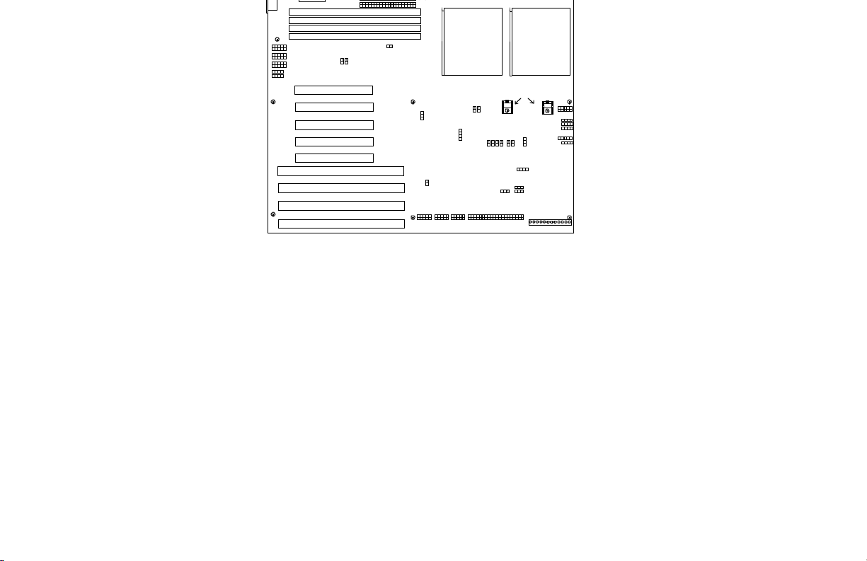
Motherboard - illustration and brief description of the
motherboard and the dual purpose expansion slot
Connectors - description of connector locations
andfunctions on the motherboard
Jumpers - detailed description of the jumpers used to
configure the motherboard
System Memory - detailed description of system
memory and how to add memory
System Memory Map - listing of traditional address
assignments for system memory
Configuration Utilities - description and instructions for
using the utility to configure the boards BIOS
Page 12

compatible with 8086/88, 80286, and 80386 DX and SX
microprocessors. In addition, the Pentium Pro features:
64-bit Data Bus
Superscalar Architecture
Capability for executing two instructions in parallel.
Pipelined Floating-Point Unit
Separate 8 KB Code and 8 KB Data Caches (total 16 KB
L1 cache)
256 KB or 512 KB internal L2 cache
Bus Cycle Pipelining
Writeback MESI Protocol in the Data Cache Internal
Parity Checking
IEEE 1149.1 Boundary Scan
It is available in a variety of speeds, from 180 MHz through
200 MHz.
For additional information, contact your authorized CSS
Laboratories representative.
Page 13
1
3V POWER
J14
J23
VRM2VRM
1
J28
J31
CN1
J1
PS/2
1
J2
SERIAL 1
1
J3
SERIAL 2
1
1
J4
USB
1
J5
USB
J8
PCI
J9
PCI
J10
PCI
J11
PCI
J12
PCI
J17
ISA
J18
ISA
J19
ISA
J20
ISA
1
J13
J14
J15
DIMM
J16
JP1
1
1
JP2
J24
1
J25
JP3
PS/2
1 1
J26 J27 J29 J30
1
INFRARED
JP24
1
Processor
JP5 JP6
1
JP7
SERIAL 2
SERIAL 1
1 1
Dual
1 1
VOLTAGE
REGULATORS
JP19
JP10
JP13
JP8
1 11 11 1
JP9
JP14
JP11
JP12 JP16
1
1
1
PARALLEL
J33
Processor
JP20
JP21
J34
JP22
JP23
JP35
JP15
1
BATTERY
JP17
5 V POWER
1
1
1
1
11
1
Figure 1: The Motherboard
Cache Memory
The processor comes with 16 KB of L1 cache, and is
available with 256 or 512 KB of internal L2 cache.
Expansion Slots
FRONT PANEL
TURBO LED/RST
IDE LED
EXT. HD LED
KEYLK/PWR LED
SPEAKER
There are a total of seven expansion slots on the
motherboard. Two slots provide 16-bit wide ISA busses.
Five of the slots are PCI bus connectors. One PCI and one
ISA are shared. Only one of these can be used at once.
3.3 Volt/5 Volt Power Regulators
Page 14

Description Connector
J35 Speaker connector
JP21 Turbo LED/Reset
J34 IDE hard drive LED
JP22 Extra IDE hard drive LED
JP20 CSS Front panel connector
J28, J31 Voltage regulator modules
CN1 Keyboard connector
J1, J26 PS/2 mouse/auxiliary keyboard
connector and auxiliary connector
JP23 Power LED/keylock
J23 Primary IDE connector
J24 Secondary IDE connector
J21, J30 Parallel port, auxiliary parallel port
J2, J29 Serial port 1, auxiliary serial port 1
J3, J27 Serial port 2, auxiliary serial port 2
J22 Floppy drive connector
J7, J33 5 volt power supply connector, auxiliary
5 volt connector
J6 3.3 volt power supply connector
J4, J5 Universal serial bus connectors
JP15 Battery connector
JP4, JP18 Fan connector
JP7 InfraRed device connector
Page 15
Pin Assignment Pin Assignment
1 Speaker 3 Gnd
2 Not used 4 VCC
Turbo LED/Reset JP21
The reset button on the front panel lets you perform a
cold boot, without turning the system off.
Pin Assignment Pin Assignment
1 Reset 3 TB LED signal
2 Not used 4 TB LED power
IDE Hard Drive LED J34; Extra IDE LED JP22
J34 or JP22 connects a hard drive access LED to the front
panel. It lights when the drive is accessed.
Pin Assignment
1 VCC
2 HDD Act (-)
3 HDD Act (-)
4 VCC
Page 16
Pin Assignment Pin Assignment
1 Ground 6 Ground
2 Power LED 7 Green LED
3 IDE Power LED 8 Keylock
4 Not used 9 Power
5 IDE LED 10 Reset
Voltage Regulator Module (VRM) J28, J31
The VRM connector, J28, connects a voltage regulation
module that adjusts the 5 volt supply. J31 connects a
voltage regulation module that adjusts the 3.3 volt supply.
Keyboard Connector CN1
Keyboard plugs are keyed for proper installation.
Pin Assignment Pin Assignment
1 Clock 4 Ground
2 Data 5 +5 Vdc
3 Not used
Page 17
Pin Assignment Pin Assignment
1 Mouse clock 6 VCC
2 Not used 7 Not used
3 Keyboard clock 8 Mouse data
4 Not used 9 Not used
5 Not used 10 Ground
Power LED/Keylock LED Connector JP23
JP23 is a 5-pin connector used to attach the motherboard
to the front panels keylock LED and power indicator LED.
Pin Assignment Pin Assignment
1 Power LED 4 Keylock
2 Not used 5 Ground
3 Ground
Primary IDE J23
J23 connects the primary on-board PCI E-IDE hard drive.
Pin 1 is marked. When connecting your E-IDE, orient pin 1
of the cable ribbon with pin 1 of J23.
Secondary IDE J24
Page 18
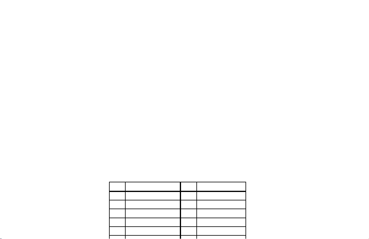
Serial Port 1 J2; Auxiliary Serial Port 1 J29
J2 or J29 provides the connection for the motherboards
serial port 1 (COM 1).
Serial Port 2 J3; Auxiliary Serial Port 2 J27
J3 or J27 provides the connection for the motherboards
serial port 2 (COM 2).
Floppy Drive Connector J22
J22 connects the floppy drive to the controller provided on
the motherboard.
5 Volt Power Supply Connector J7; Auxiliary 5 Volt
Power Connector J33
Pin Assignment Pin Assignment
1 Power good 7 Ground
2 +5 Vdc 8 Ground
3 +12 Vdc 9 -5 Vdc
4 -12 Vdc 10 Not used
5 Ground 11 +5 Vdc
Page 19
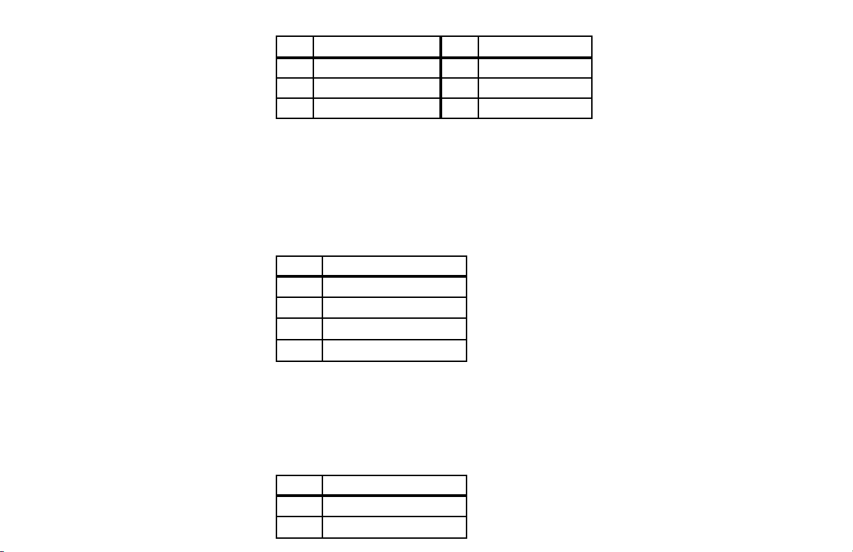
3.3 Volt Power Supply Connector J6
Pin Assignment Pin Assignment
1 Ground 4 +3.3 Vdc
2 Ground 5 +3.3 Vdc
3 Ground 6 +3.3 Vdc
Universal Serial Bus Connectors J2, J3
The motherboard provides two 4-pin universal serial bus
(USB) connectors.
Pin Assignment
1 VCC
2 Data -
3 Data +
4 Ground
Fan Connectors JP4, JP18
The processor fan provides extra cooling for the powerful
Pin Assignment
1 12 volt
2 Ground
Page 20
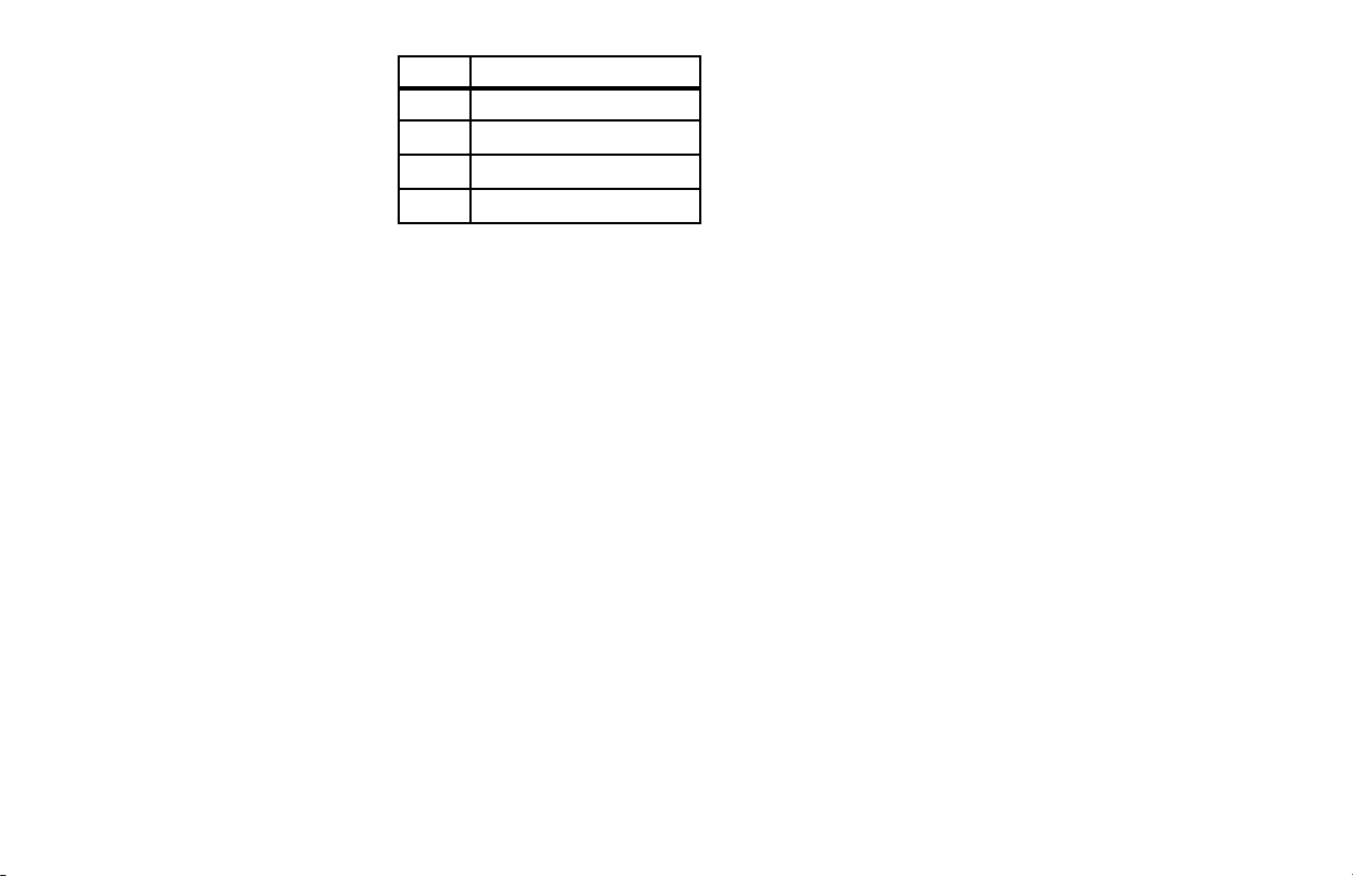
peripheral devices including mouse, printer and keyboard.
Pin Assignment
1 Transmitting
2 Receive 1
3 Receive 2
4 Ground
Page 21
Read the following section carefully, before configuring your
system.
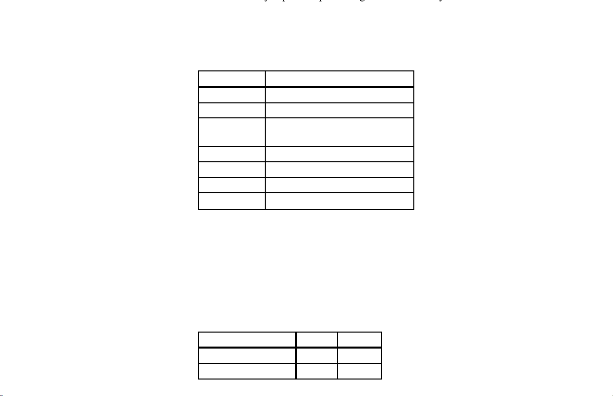
The motherboard has the following jumpers:
Jumper Description
JP5, JP6 Processor bus clock speed
JP1, JP2 Processor bus frequency
JP8, JP9 Processor speed ratio
JP10, JP11
JP16, JP17 Flash BIOS enable
JP3 ISA bus speed
JP13 Manual EXTSMI
JP14 DBX controlled EXTSMI
Processor Bus Clock Speed JP5, JP6
Pentium Pro processors are designed with one of two bus
clock speeds. The bus clock speed is always a fraction of
the processors internal speed. The table on page 13 will
help you determine the correct setting for your system.
Bus Clock Speed JP5 JP6
60 MHz IN OUT
66 MHz OUT IN
Page 22
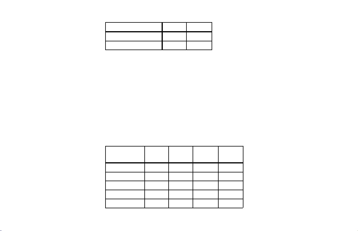
the processors speed. The table on page 13 will help you
determine the correct setting for your system.
Bus Frequency JP1 JP2
60 MHz IN OUT
66 MHz OUT IN
Processor Speed Ratio JP8, JP9, JP10, JP11
The Pentium Pro uses a clock multiplier to run at a speed
faster than the processor bus.
These jumpers match the installed processors speed with
the motherboards defined processor speed. When upgrading,
you may need to adjust them. The table on page 13 will
help you determine the correct setting for your system.
Processor JP8 JP9 JP10 JP11
Speed Ratio
2x IN IN IN IN
2.5x IN IN IN OUT
3x IN IN OUT IN
3.5x IN IN OUT OUT
4x IN OUT IN IN
Page 23
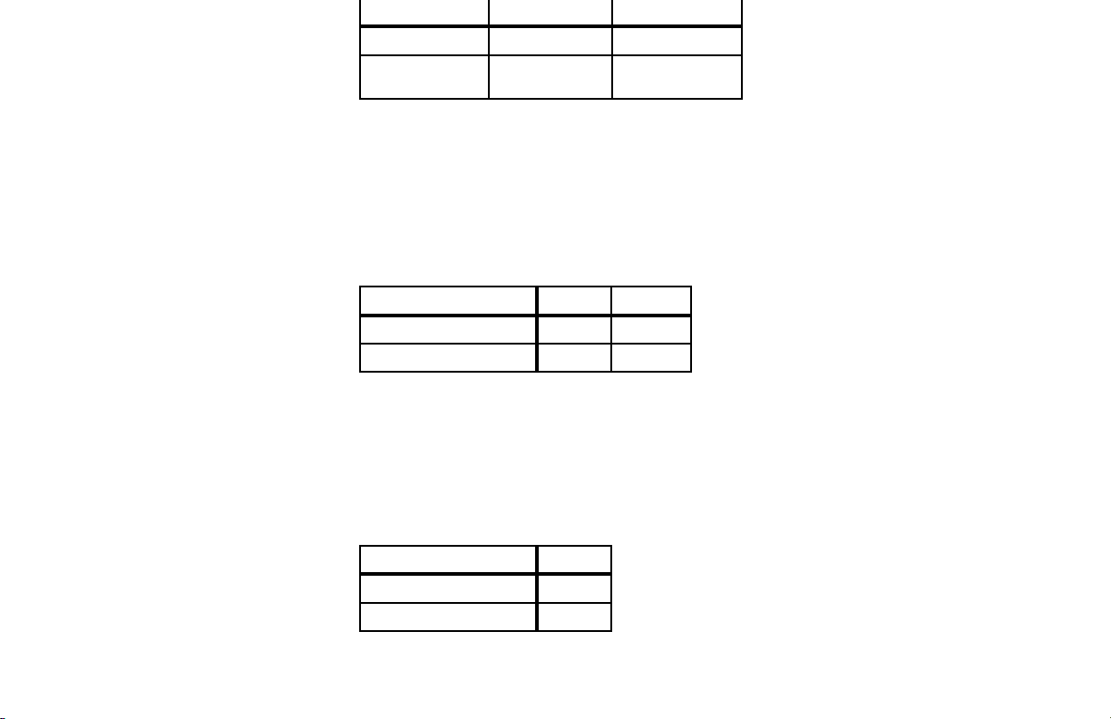
Type/Speed Bus Speed
180 MHz 3x 60 MHz
200 MHz 3x 66 MHz
Flash BIOS Enable JP16, JP17
These jumpers let you use flash BIOS, loading the latest
version of BIOS. Be careful to return the settings to their
default values after you have loaded the flash BIOS.
Flash BIOS Enable JP16 JP17
Non-Flash 2-3 1-2
Flash (default) 1-2 2-3
ISA Bus Speed JP3
The ISA bus uses the processors oscillator to set its speed.
This jumper is set at the factory to the correct value.
ISA Bus Speed JP20
Divide by 3 1-2
Divide by 4 (default) 2-3
Page 24
mode. This procedure is sometimes used in specific system
testing.
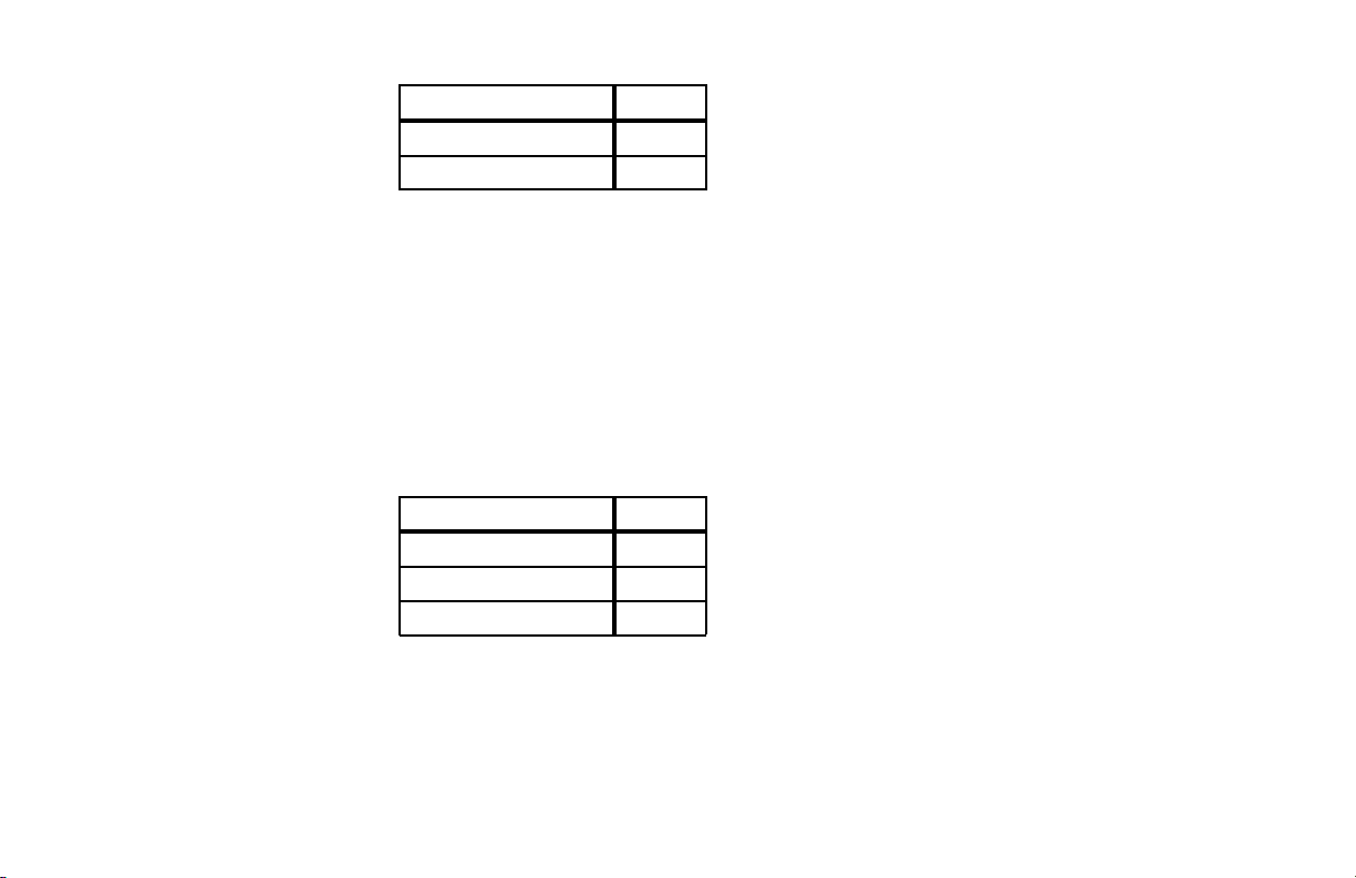
Manual EXTSMI JP13
Forced Sleep IN
Normal (default) OUT
DBX Controlled EXTSMI JP14
The DBX controlled external system management interrupt
(SMI) jumper allows a technician to bypass the BIOS SMI
control and to use the motherboards chipset to control the
SMI. This procedure is sometimes used in specific system
testing.
DBX EXTSMI JP14
DBX controlled IN
BIOS controlled OUT
(default)
Page 25

correcting code (ECC).
There are a total of four banks available for memory
upgrades. The board supports DIMM in the following
combinations:
1M x 64/72 = 8 MB/bank 8M x 64/72 = 64 MB/bank
2M x 64/72 = 16 MB/bank 16M x 64/72 = 128 MB/bank
4M x 64/72 = 32 MB/bank 32M x 64/72 = 256 MB/bank
Installing and Removing DIMM
Read these instructions completely before installing or
removing DIMMs. The DIMM is held by plastic press-clips
on both sides of the slot.
Installing DIMM
1) Hold the DIMM so that the gold tab is pointing toward the
slot. The DIMM is keyed so that it will only snap into the
slot when positioned correctly.
2) Press one end of the DIMM until it inserts and its press-
clip snaps into place.
3) Press the other end of the DIMM until it inserts and its
press-clip snaps into place.
Page 26

8 MB 1M x 64/72
16 MB 1M x 64/72 1M x 64/72
16 MB 2M x 64/72
24 MB 1M x 64/72 1M x 64/72 1M x 64/72
24 MB 1M x 64/72 2M x 64/72
32 MB 1M x 64/72 1M x 64/72 1M x 64/72 1M x 64/72
32 MB 2M x 64/72 2M x 64/72
32 MB 4M x 64/72
32 MB 2M x 64/72 1M x 64/72 1M x 64/72
32 MB 2M x 64/72 2M x 64/72
40 MB 1M x 64/72 2M x 64/72 2M x 64/72
40 MB 1M x 64/72 4M x 64/72
40 MB 2M x 64/72 1M x 64/72 1M x 64/72 1M x 64/72
48 MB 4M x 64/72 1M x 64/72 1M x 64/72
48 MB 2M x 64/72 2M x 64/72 2M x 64/72
48 MB 2M x 64/72 4M x 64/72
48 MB 4M x 64/72 1M x 64/72 1M x 64/72
48 MB 4M x 64/72 2M x 64/72
56 MB 1M x 64/72 2M x 64/72 2M x 64/72 2M x 64/72
56 MB 4M x 64/72 1M x 64/72 1M x 64/72 1M x 64/72
64 MB 2M x 64/72 2M x 64/72 2M x 64/72 2M x 64/72
64 MB 8M x 64/72
64 MB 4M x 64/72 4M x 64/72
64 MB 4M x 64/72 2M x 64/72 2M x 64/72
64 MB 4M x 64/72 4M x 64/72
72 MB 8M x 64/72 1M x 64/72
72 MB 1M x 64/72 4M x 64/72 4M x 64/72
Page 27

96 MB 4M x 64/72 4M x 64/72 4M x 64/72
96 MB 4M x 64/72 8M x 64/72
104 MB 1M x 64/72 4M x 64/72 4M x 64/72 4M x 64/72
112 MB 2M x 64/72 4M x 64/72 4M x 64/72 4M x 64/72
128 MB 4M x 64/72 4M x 64/72 4M x 64/72 4M x 64/72
128 MB 8M x 64/72 8M x 64/72
128 MB 16M x 64/72
136 MB 16M x 64/72 1M x 64/72
136 MB 1M x 64/72 8M x 64/72 8M x 64/72
144 MB 2M x 64/72 16M x 64/72
144 MB 2M x 64/72 8M x 64/72 8M x 64/72
144 MB 16M x 64/72 1M x 64/72 1M x 64/72
152 MB 16M x 64/72 1M x 64/72 1M x 64/72 1M x 64/72
160 MB 16M x 64/72 2M x 64/72 2M x 64/72
160 MB 16M x 64/72 4M x 64/72
160 MB 4M x 64/72 8M x 64/72 8M x 64/72
176 MB 16M x 64/72 2M x 64/72 2M x 64/72 2M x 64/72
192 MB 8M x 64/72 8M x 64/72 8M x 64/72
192 MB 16M x 64/72 4M x 64/72 4M x 64/72
192 MB 16M x 64/72 8M x 64/72
200 MB 1M x 64/72 8M x 64/72 8M x 64/72 8M x 64/72
208 MB 2M x 64/72 8M x 64/72 8M x 64/72 8M x 64/72
224 MB 4M x 64/72 8M x 64/72 8M x 64/72 8M x 64/72
224 MB 16M x 64/7 24M x 64/7 24M x 64/72 4M x 64/72
256 MB 8M x 64/72 8M x 64/72 8M x 64/72 8M x 64/72
256 MB 16M x 64/72 16M x 64/72
256 MB 32M x 64/72
256 MB 16M x 64/72 8M x 64/72 8M x 64/72
Page 28

272 MB 2M x 64/72 16M x 64/72 16M x 64/72
280 MB 32M x 64/72 1M x 64/72 1M x 64/72 1M x 64/72
288 MB 32M x 64/72 4M x 64/72
288 MB 32M x 64/72 2M x 64/72 2M x 64/72
288 MB 4M x 64/72 16M x 64/72 16M x 64/72
304 MB 32M x 64/72 2M x 64/72 2M x 64/72 2M x 64/72
320 MB 32M x 64/72 4M x 64/72 4M x 64/72
320 MB 16M x 64/72 8M x 64/72 8M x 64/72 8M x 64/72
320 MB 32M x 64/72 8M x 64/72
352 MB 32M x 64/72 4M x 64/72 4M x 64/72 4M x 64/72
384 MB 16M x 64/72 16M x 64/72 16M x 64/72
384 MB 16M x 64/72 32M x 64/72
384 MB 32M x 64/72 8M x 64/72 8M x 64/72
392 MB 1M x 64/72 16M x 64/72 16M x 64/72 16M x 64/72
400 MB 2M x 64/72 16M x 64/72 16M x 64/72 16M x 64/72
416 MB 4M x 64/72 16M x 64/72 16M x 64/72 16M x 64/72
448 MB 32M x 64/72 8M x 64/72 8M x 64/72 8M x 64/72
512 MB 16M x 64/72 16M x 64/72 16M x 64/72 16M x 64/72
512 MB 32M x 64/72 32M x 64/72
512 MB 32M x 64/72 16M x 64/72 16M x 64/72
520 MB 1M x 64/72 32M x 64/72 32M x 64/72
528 MB 2M x 64/72 32M x 64/72 32M x 64/72
544 MB 4M x 64/72 32M x 64/72 32M x 64/72
640 MB 16M x 64/72 32M x 64/72 32M x 64/72
640 MB 32M x 64/72 16M x 64/72 16M x 64/72 16M x 64/72
768 MB 32M x 64/72 32M x 64/72 32M x 64/72
776 MB 1M x 64/72 32M x 64/72 32M x 64/72 32M x 64/72
Page 29
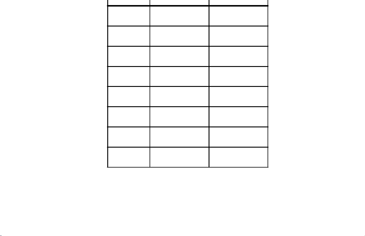
000000 to
9FFFFF
640 KB motherboard system memory
0A0000 to
0BFFFF
0C0000 to
0DFFFF
0E0000 to
0EFFFF
0F0000 to
0FFFFF
100000 to
FDFFFF
FE0000 to
FEFFFF
FF0000 to
FFFFFF
128 KB video display
ROM
128 KB I/O
expansion ROM
64 KB reserved on
motherboard
64 KB ROM on
motherbord
maximum memory is
15 MB
64 KB reserved on
motherboard
64 KB reserved on
motherboard
reserved for graphics
reserved for ROM on
I/O
duplicate code
assignment at FE0000
duplicate code
assignment at FF0000
I/O channel memory
duplicate code
assignment at 0E0000
duplicate code
assignment at 0F0000
Timers
The systems three programmable timers/counters controlled
by timer/counter chips are defined as channels 0
through 2 as indicated below:
Channel 0: System Timer
Page 30
Below are assignments in decreasing priority.
LEVEL FUNCTION
Microprocessor NMI Parity or I/O Channel Check
Interrupt Controllers
Ctlr 1 Ctlr 2
IRQ0
IRQ1
IRQ2
*Interrupts IRQ8 - IRQ15 redirected to IRQ2*
IRQ8 Real-Time clock interrupt
IRQ9 Software re-directed to INT + AH (IRQ2)
IRQ10 Reserved
IRQ11 Reserved
IRQ12 Reserved
IRQ13 Coprocessor
IRQ14 Fixed disk controller
IRQ15 Reserved
IRQ3 Serial port 2
IRQ4 Serial port 1
IRQ5 Parallel port2
IRQ6 Diskette controller
IRQ7 Parallel port 1
Page 31
boards do not require IRQs. Some can share an IRQ with
another board of the same model and manufacture. Check the
add-in boards documentation for IRQ information.
Direct Memory Access
The system supports seven DMA channels:
Controller 1 Controller 2
Channel 0 - Spare Channel 4 - Cascade
for Controller 1
Channel 1 - SDLC Channel 5 - Spare
Channel 2 - Diskette Channel 6 - Spare
Channel 3 - Spare Channel 7 - Spare
The first DMA controller holds channels 0 through 3. These
channels support 8-bit data transfers between 8-bit I/O
adapters and 8- or 16-bit system memory. Each channel can
transfer data in 4 KB blocks.
The second DMA controller holds channels 4 through 7.
Channel 4 cascades channels 0 through 3 to the
microprocessor. Channel 5, 6 and 7 support 16-bit data
transfers between 16-bit I/O adapters and 16-bit system
memory. These DMA channels can transfer data throughout
the 16 MB system-address space in 128 KB blocks.
Page 32

000-01F DMA #1
020-03F INTR #1
040-05F Timer
060-06F Keyboard
070-07F NMI mask register
080-09F DMA page register
0A0-OBF INTR #2
0C0-ODF DMA #2
0F0-0F1 Clr/rst math coprocessor
0F8-0FF Math coprocessor
1F0-1F8 Fixed disk
200-207 Joystick
278-27F Secondary parallel port
2F8-2FF Secondary serial port
300-31F Prototype card
378-37F Primary parallel port
380-38F SDLC (secondary bisynchronous)
3A0-3AF Primary bisynchronous
3B0-3BF Monochrome display/printer adapter
3D0-3DF Color/graphics monitor adapter
3F0-3F7 Diskette controller
3F8-3FF Primary serial port
Page 33
BIOS Setup is a utility that defines and stores the
configuration of the machine. When the system boots, the
machines configuration loads into memory. Drives, video
adapter, memory and keyboard are described to the system.
The program is built into the CMOS chip on the
motherboard. To start the program, press the <Delete> key
while the system is booting. The Utilities menu displays:
ROM PCI/ISA BIOS
CMOS SETUP UTILITY
AWARD SOFTWARE, INC.
STANDARD CMOS SETUP INTEGRATED PERIPHERALS
BIOS FEATURES SETUP SUPERVISOR PASSWORD
CHIPSET FEATURES USER PASSWORD
POWER MANAGEMENT SETUP IDE HDD AUTO DETECTION
PnP PCI CONFIGURATION SETUP HDD LOW LEVEL FORMAT
LOAD BIOS DEFAULTS SAVE & EXIT SETUP
LOAD SETUP DEFAULTS EXIT WITHOUT SAVING
Esc: Quit : Select Item
F10 : Save & Exit Setup (Shift)F2 : Change Color
Time, Date, Hard Disk Type...
Figure 2: The Main Menu
If you discover after making and saving system changes that
you have made a mistake, the BIOS lets you override the
Page 34

Selection Description
Standard CMOS SetupStandard options for the
computer.
BIOS Features Setup Enhanced BIOS options.
Chipset FeaturesSetup Options for the motherboards
chipset.
Power Management Setup Advanced Power Management
(APM) options.
PnP/PCIConfiguration Plug and Play standard and PCI
Local Bus configuration options.
Integrated Peripherals I/O subsystems that depend on
integrated peripherals
controller on the motherboard.
Supervisor/User Password Change, set or disable a
password. Only the supervisor
password accesses Setup.
IDE HDD Auto Detection Automatically detect and
configure IDE hard disk
parameters.
HDD Low Level Format CSS strongly recommends you
do not low-level format your
hard drive. This may overwrite
the bad-track table.
Load BIOS Defaults BIOS defaults are factory
settings for the most stable,
minimal-performance.
Load Setup Defaults Setup defaults are factory
settings for optimal-performance
operations.
Save & Exit Setup Save settings in CMOS and exit
the program.
Page 35
ROM PCI/ISA BIOS
CMOS SETUP UTILITY
AWARD SOFTWARE, Inc.
Date (mm/dd/yy) : Friday, March 3, 1997
Time (hh/mm/ss) : 11:11:00
Pri Master Auto
Pri Slave Auto
Sec Master Auto
Sec Slave Auto
Floppy Drive A : 1.44 MB 3 1/2
Floppy Drive B : Not Installed
Video: EGA/VGA
Halt On : All Errors
Esc: Quit : Select Item PgUp/PgDn : Modify
F10 : Save & Exit Setup <Shift> F2 : Change Color
Type Size Cyls Head Precomp LandZ Sect Mode
Base Memory: 640K
Extended Memory: 48182K
Other Memory: 384K
Total Memory: 49152K
Figure 3: The Standard Setup Menu
The values represented in this table are used as an example,
and may not match your BIOS settings.
The Setup Procedure
To start Setup, highlight STANDARD CMOS SETUP on
the Main Menu, and press <ENTER>. The current system
configuration stored in CMOS is displayed. The screen
image displayed in figure X is an example, and may differ
Page 36
Key Action
Left and right arrows Moves the cursor left to right and
right to left.
Up and down arrows Moves cursor up and down, and
from field to field.
<Enter> Selects the setting and moves
cursor to next field.
<F10> Saves the settings and exits
Setup.
<Esc> Exit to main screen from
submenu.
<F1> Help.
In order to use the <PgUp> and <PgDn> keys on the
numeric key pad, you must turn the <NumLock> off.
Alter only the items that need to be changed or reset. If a
highlighted option is correct, skip the corresponding step.
1) Start by entering the current date in the following format:
mm/dd/yy. March 3, 1991 would be entered as 03/03/91.
Press <Enter> to continue.
2) Enter the current time using the military style: hh:mm:ss.
4:11 p.m. is entered as 16:11:00. Press <Enter> to
continue.
Page 37

- 2.88 MB
After you find your floppy drive type, press the <Enter>
key. Repeat this procedure for Floppy drive B:, or press
<Enter> again to skip to the next step.
4) Use the <PgUp> and <PgDn> keys to toggle between the
different hard drive types.
The lower right hand side of the Setup menu displays
information about your system board:
Base Memory Size The amount of base (conventional)
memory, 0 to 640 KB.
Extended Memory The amount of expansion memory
Size extended beyond base memory.
Other Memory Any other type of memory, usually
the memory above base and below
1 MB.
When you have made all the necessary changes, verify that
the settings are correct. Press the <Esc> key. The screen
displays the following:
Write data into CMOS and exit (Y/N)? Y
Type Y or N, and press <Enter>. Entering N will
Page 38
at the factory.
ROM PCI/ISA BIOS
BIOS FEATURES SETUP
AWARD SOFTWARE, INC.
Virus Warning: Disabled Video BIOS Shadow: Enabled
CPU Internal Cache: Enabled C8000-CBFFF Shadow: Disabled
External Cache: Enabled CC000-CFFFF Shadow: Disabled
Quick POST: Disabled D0000-D3FFF Shadow: Disabled
Boot Sequence: A, C D4000-D7FFF Shadow: Disabled
Swap Floppy Drive: Disabled D8000-DBFFF Shadow: Disabled
Boot Up Floppy Seek : Enabled DC000-DFFFF Shadow: Disabled
Boot Up NumLock Status : On
Boot Up System Speed : High
Gate A20 Option: Fast
Memory Parity Check: Disabled
Typematic Rate Setting: Disabled
Typematic Rate (Chars/Sec): 6
Typematic Delay: 250
Security Option: Setup
Esc : Quit : Select Item
PCI/VGA Palette Snoop: Disabled
OS Select-DRAM>64MB: Non-
OS/2
F1 : Help PU/PD/+/- : Modify
F5 : Old Values (Shift)F2 : Color
F6 : Load BIOS Defaults
F7 : Load Setup Defaults
Figure 4: BIOS Features Setup
The values represented in this table are used as an
example, and may not match your BIOS settings.
Page 39
set at the factory. The settings need only be changed if you
are reconfiguring the system.
ROM PCI/ISA BIOS
CHIPSET FEATURES SETUP
AWARD SOFTWARE, INC.
Auto Configuration : Enabled
DRAM Speed Selection : 70 ns
DRAM RAS# Precharge Time : 4
DRAM R/W Leadoff Timing : 7/6
Fast RAS# to CAS# Delay : 3
DRAM Read Burst EDO/EPP: x333/x444
DRAM Write Burst Timing : x333
Turbo Read Leadoff : Disabled
DRAM Speculative Leadoff : Disabled
ISA Bus Clock : PCICLK4
System BIOS Cacheable : Enabled
Video BIOS Cacheable : Enabled
8 Bit I/O Recovery Time : 1
16 Bit I/O Recovery Time : 1
Memory Hole At 15M - 16M: Disabled
Peer Concurrency: Enabled
Chipset Special Features : Enabled
DRAM ECC/Parity Select : ECC
Memory Parity/ECC Check : Auto
Single Bit Error Report : Enable
L2 Cache Cacheable Size : 64MB
Chipset NA# Asserted : Enabled
Pipeline Cache Timing : Faster
Esc : Quit : Select Item
F1 : Help PU/PD/+/- : Modify
F5 : Old Values (Shift)F2 : Color
F6 : Load BIOS Defaults
F7 : Load Setup Defaults
Figure 5: BIOS Features Setup
The values represented in this table are used as an
example, and may not match your BIOS settings.
Page 40
ROM PCI/ISA BIOS
POWER MANAGEMENT SETUP
AWARD SOFTWARE, INC.
Power Management : Max Savings IRQ3 (COM2) : OFF
PM Control by APM : Yes IRQ4 (COM1) : ON
Video Off Method :V/H Sync&Blank IRQ5 (LPT2) : OFF
Modem Use IRQ : 3 IRQ6 (Floppy Disk) : ON
IRQ7 (LPT1) : OFF
Doze Mode : 1 minute IRQ8 (RTC Alarm) : ON
Standby Mode : 1 minute IRQ9 (IRQ8 Redir) : OFF
Suspend Mode : 1 minute IRQ10 (Reserved) : OFF
HDD Power Down Mode: 1 minute IRQ11 (Reserved) : OFF
IRQ12 (PS/2 Mouse) : OFF
*Wake Up Events In Doze&Standby* IRQ13 (Coprocessor) : OFF
IRQ3 Wakeup Event: OFF IRQ14 (Hard Disk) : ON
IRQ4 Wakeup Event: ON IRQ15 (Reserved) : OFF
IRQ8 Wakeup Event: OFF
IRQ12 Wakeup Event: OFF
Esc : Quit : Select Item
F1 : Help PU/PD/+/- : Modify
F5 : Old Values (Shift)F2 : Color
F6 : Load BIOS Defaults
F7 : Load Setup Defaults
Figure 6: Power Management Setup
The following pages provide descriptive overviews of each
option in the Power Management Setup.
Page 41

brief description of both.
Max Saving: Maximum power savings (SL processors only).
User Defined: Set each mode individually. Select time-out
periods in PM Timers section.
Min Savings: Minimum savings. Inactivity period is 1 hour.
in each mode, except hard drive.
PM Controlby APM
If Advanced Power Management APM) isinstalled, selecting
Yes gives better power savings.
Video Off Method Determines the manner in which the
monitor is blanked.
V/H SYNC+Blank: System turns off vertical and horizontal
synchronization ports and writes blanks to the video buffer.
DPMS Support: Select this option if your monitor supports
the Display Power Management Signaling (DPMS) standard.
Use the software supplied with the video subsystem to select
video power management values.
Blank Screen: System only writes blanks to the video buffer.
MODEM Use IRQs
Page 42

Management mode.
Doze Mode: After the selected period of inactivity, 1 minute
to 1 hour, the processor clock runs at slower speed while all
other devices continue to operate at full speed.
Standby Mode: After the selected period of inactivity, 1
minute to 1 hour, the fixed disk and video shut off while all
other devices continue to operate at full speed.
Suspend Mode: After the selected period of system inactivity,
1 minute to 1 hour, all devices except the processor shut off.
HDD Power Down: After the selected period of drive
inactivity, 1 to 15 minutes, the hard disk drive powers down
while all other devices remain active.
Wake Up Events
You can turn on or off monitoring of four commonly used
interrupt requests so they do not awaken the system from, or
reset activity timers for Doze and Standby modes.
For example, if you have a modem on IRQ3, you can turn on
IRQ3 as a wake-up event, so that an interrupt from the
modem can wake up the system.
Or you may want to turn off IRQ12, the PS/2 mouse, as a
wake-up event, so accidently brushing the mouse does not
awaken the system. The default wake-up event is keyboard
Page 43

mode.
IRQ3 - COM2 IRQ10 - Reserved
IRQ4 - COM1 IRQ11 - Reserved
IRQ5 - LPT2 IRQ12 - PS2/Mouse
IRQ6 - Floppy IRQ13 - Coprocessor
IRQ7 - LPT1 IRQ14 - Hard disk
IRQ8 - RTC IRQ15 - Reserved
IRQ9 - IRQ2 redir.
Power Management Setup allows you to take advantage of
Microsofts DOS 6.2
TM
Advanced Power Management
(APM) program.
The values represented in this table are used as an example,
and may not match your BIOS settings. To take advantage of
this feature,
Make sure DOS 6.2 is installed on your system
Select YES for PM Control by APM in the menu above
Enable the DOS Power program
Enable the Power program in Windows 3.1
TM
, if installed
Page 44

1) Open your CONFIG.SYS file by using a text editor, such
as MS-DOS Editor. To open your CONFIG.SYS file
using MS-DOS Editor, type the following at the
command prompt: edit c:\config.sys
2) At the end of the CONFIG.SYS file, add a device
command specifying the location of the POWER.EXE
file. This example specifies the POWER.EXE file is
located in the C: drive DOS directory, and that the default
setting should be used: device=c:\dos\power.exe
3) Save the changes to your CONFIG.SYS file, and quit the
text editor.
4) Restart the computer. Press <CTRL> <ALT> <DEL>.
MS-DOS 6.2 Users Guide also provides instructions. For
more information, type help power, at the DOS prompt.
Windows 3.1TM Advanced Power Management
Use the Windows Setup program to select the MS-DOS
with APM option.
1) Start the Windows Setup program by changing to the
Windows root directory and typing Setup: cd windows
setup.
2) At the Windows Setup menu, edit the Computer field.
Page 45

4) Accept the change and exit the Setup program. Restart
your computer by pressing <CTRL> <ALT> <DEL>.
Windows 95
TM
Advanced Power Management
1) Enable the APM option in BIOS Setup before installing
Windows 95.
2) The APM is automatically installed during Windows 95
setup.
3) An APM icon appears in the Control Panel window,
indicating a successful installation.
Page 46
The values represented in this table are used as an example,
and may not match your BIOS settings.
ROM PCI/ISA BIOS
PnP/PCI CONFIGURATION SETUP
AWARD SOFTWARE, INC.
Resources Controlled By: Manual PCI IRQ Activated By : Level
Reset Configuration Data: Disabled PCI IDE IRQ Map To : PCI-AUTO
IRQ-3 Assigned to : Legacy ISA Primary IDE INT# : A
IRQ-4 Assigned to : Legacy ISA
IRQ-5 Assigned to : PCI/ISA PnP
IRQ-7 Assigned to : PCI/ISA PnP
IRQ-9 Assigned to : PCI/ISA PnP
IRQ-10 Assigned to : PCI/ISA PnP
IRQ-12 Assigned to : PCI/ISA PnP
IRQ-14 Assigned to : PCI/ISA PnP
IRQ-15 Assigned to : PCI/ISA PnP
DMA-0 Assigned to : PCI/ISA PnP
DMA-1 Assigned to : PCI/ISA PnP
DMA-3 Assigned to : PCI/ISA PnP
DMA-5 Assigned to : PCI/ISA PnP
DMA-6 Assigned to : PCI/ISA PnP
DMA-7 Assigned to : PCI/ISA PnP
Secondary IDE INT# : B
Esc : Quit : Select Item
F1 : Help PU/PD/+/- : Modify
F5 : Old Values (Shift)F2 : Color
F6 : Load BIOS Defaults
F7 : Load Setup Defaults
Figure 7: Plug and Play/PCI Setup
Page 47
E-IDE controller and drives, universal serial bus (USB)
controller, floppy controller, serial ports and parallel port.
ROM PCI/ISA BIOS
INTEGRATED PERIPHERALS SETUP
AWARD SOFTWARE, INC.
IDE HDD Block Mode : Enabled
PCI Slot IDE 2
On-Chip Primary PCI IDE : Enabled
On-Chip Secondary PCI IDE : Enabled
IDE Primary Master PIO : Enabled
IDE Primary Slave PIO : Enabled
IDE Secondary Master PIO : Enabled
IDE Secondary Slave PIO : Enabled
USB Controller : Enabled
Onboard FDC Controller : Enabled
Onboard Serial Port 1 : COM1/3F8
Onboard Serial Port 2 : COM2/2F8
Onboard Parallel Port : 378/IRQ7
Parallel Port Mode : Compatible
ECP Mode Use DMA : 0
EPP Version : 1.7
InfraRed Duplex Type : Disabled
nd
Channel : Enabled
Figure 8: Integrated Peripherals Configuration Setup
Esc : Quit : Select Item
F1 : Help PU/PD/+/- : Modify
F5 : Old Values (Shift)F2 : Color
F6 : Load BIOS Defaults
F7 : Load Setup Defaults
 Loading...