

Page 1

LK\
CDB5471
CDB5471 Evaluation Board and Software
Features
l Direct Shunt Sensor and Current
Transformer Interface for 3-Phase
Power
l On-Board Voltage Reference
l On-board crystal for XIN
l Digital Interface to PC
l Lab Windows/CVI
Evaluation
Software
- “Real-Time” RMS calculation
- FFT Analysis
- Time Domain Analysis
- Noise Histogram Analysis
General Description
The CDB5471 is an inexpensi ve tool des igned to ev al uate the functionality/performance of the CS5471 2channel A/D Converter. In addition to this data sheet, the
CS5471 Data Sheet is requir ed in conjunction with the
CDB5471 Evaluation Board.
Two terminal-block connectors serve as inputs to the
CS5471’s two analog input pairs. The CDB5471 includes an optional voltage reference source for CS5471.
A 4.096MHz crystal is provided as a source for CS5471’s
XIN pin, or an exte rnal c lock s ource can b e sup plied by
the user. Digital o utput data fro m the CS5471 is transferred to the user’s IBM-com patible PC vi a the include d
25-pin parallel port cable.
The CDB5471 includes PC software, allowing the user to
perform data capture (includes option for time domain
analysis, histogram analysis, and frequency domain
analysis). The software also allows real-time RMS calculation/analysis to be performed simultaneously on the
instantaneous data from both chann els .
ORDERING INFORMATION
CDB5471 Evaluation Board
VIN1+
VIN1IIN1+
IIN1-
VIN2+
VIN2IIN2+
IIN2-
VIN3+
VIN3IIN3+
IIN3-
V
REF
Voltage
Reference
Preliminary Product Information
P.O. Box 17847, Austin, Texas 78760
(512) 445 7222 FAX: (512) 445 7581
http://www.cirrus.com
VA-
Charge
Pump
Circuitry
CPD
VA-
VA+
GAIN
OWRS
RESET
FSO
SDO
CLK
CS5451
V
REF
IN OUT
XIN
+5 VINVA+
3 V
Regulator
(Not Populated)
SE
Header
Control Switches
Reset Circ uit
Serial-to-
Parallel
Interface
Crystal
4.096 MHz
VD+GND
DB25
To PC
This document contains information for a new product.
Cirrus Logic reserves the right to modify this product without notice.
Copyright Cirrus Logic, Inc. 2001
(All Rights Reserved)
FEB ‘01
DS480DB1
1
Page 2

TABLE OF CONTENTS
1. INTRODUCTION ....................................................................................................................... 4
1.1 CS5471 ..............................................................................................................................4
1.2 Data Flow on Evaluation Board .........................................................................................4
2. HARDWARE ............................................................................................................................. 5
2.1 Evaluation Board Description ............................................................................................. 5
2.2 Power Supply Connections ................................................................................................5
2.2.1 Analog Power Supply ............................................................................................5
2.2.2 Digital Power Supply .............................................................................................5
2.2.3 Charge Pump Options ........................................................................................... 6
2.3 Eval Board Control - Headers/Switches .............................................................................6
2.3.1 Analog Inputs ........................................................................................................ 8
2.3.2 Voltage Reference Input .......................................................................................9
2.3.3 Clock Source for XIN ................. ...... ....... ...... ...... ....... ...... ....... ...... .........................9
2.3.4 S1 DIP Switch ....................................................................................................... 9
2.3.5 Reset Circuit .......................................................................................................... 9
2.3.6 External Signal In/Out Header ..............................................................................9
2.3.7 Serial-to-Parallel Interface .....................................................................................9
2.3.8 Connecting the Eval Board to PC .......................................................................10
3. SOFTWARE ............................................................................................................................ 14
3.1 Installing the Software ...................................................................................................... 14
3.2 Running the Software ......................................................................................................14
3.2.1 Getting Started ....................................................................................................14
3.2.2 The Start-Up Window ..........................................................................................15
3.2.3 The Conversion Window ..................................................................................... 15
3.2.4 Data Collection Window ......................................................................................17
3.2.5 Config Window .................................................................................................... 18
3.2.6 Analyzing Data ....................................................................................................19
3.2.7 Time Domain Information ....................................................................................19
3.2.8 Frequency Domain Information ...........................................................................20
3.2.9 Histogram Information .........................................................................................21
CDB5471
Contacting Cirrus Logic Support
For a complete listing of Direct Sales, Distributor, and Sales Representative contacts, visit the Cirrus Logic web site at:
http://www.cirrus.com/corporate/contacts/sales.cfm
IBM, AT and PS/2 are trademarks of International Business Machines Corporation.
Windows is a trademark of Microsoft Corporation.
Lab Windows and CVI are trademarks of National Instruments.
TM
SPI
is a trademark of Motorola.
TM
Microwire
Preliminary product inf o rmation describes products whi c h are i n p r od uct i on, but for which full char acterization data is not yet avai l ab le . Advance p r odu ct i nfor -
mation describes products which are in development and subject to development changes. Cirrus Logic, Inc. has made best efforts to ensure that the information
contained in this document i s accurat e and reli able. However , t he infor mation is subje ct to chang e without noti ce and is provi d ed “AS IS” without warrant y of
any kind (express or implied). No responsibility is assumed by Cirrus Logic, Inc. for the use of this information, nor for infringements of patents or other ri g ht s
of third parties. This document is the pro perty of Cirrus Logi c, Inc. and i mplie s no licen se under patents, copyrights, tr ademarks, or trade secre ts. No part of
this publication may be copied, reproduced , stored in a retrieval system, or transmitted, in any form or by any means (electronic, mechanical, photographic, or
otherwise) without the pr i or writ ten consent of Cirrus Logic, Inc. Items from any Cirrus Logic website or di sk may be printed for use by the user. However, no
part of the printout or electronic files may be copied, reproduced, stored in a retrieval system, or transmitted, in any form or by any means (electronic, mechanical,
photographic, or otherwise) without the prior written consent of Cirrus Logic, Inc.Furthermore, no part of this publication may be used as a basis for manufacture
or sale of any items without the prior written consent of Cirrus Logic, Inc. The names of products of Cirrus Logic, Inc. or other vendors and suppliers appearing
in this document may be trademarks or service marks of their respective owners which may be registered in some jurisdictions. A list of Cirrus Logic, Inc. trademarks and service marks can be found at http://www.cirrus.com.
2 DS480DB1
is a trademark of National Semiconductor.
Page 3

LIST OF FIGURES
Figure 1. Power Supply, CS5471, and Oscillator ..............................................11
Figure 2. Analog Inputs ..................................................................................... 12
Figure 3. Digital Circuitry ...................................................................................13
Figure 4. Start-Up Window................................................................................ 15
Figure 5. Conversion Window ........................................................................... 16
Figure 6. Data Collection Window (Time Domain) ............................................17
Figure 7. Configuration Window........................................................................ 19
Figure 8. Data Collection Window (FFT)........................................................... 20
Figure 9. Data Collection Window (Histogram) ................................................. 21
Figure 10.Silkscreen ...........................................................................................22
Figure 11.Circuit Side .........................................................................................23
Figure 12.Solder Side......................................................................................... 24
CDB5471
DS480DB1 3
Page 4

CDB5471
1. INTRODUCTION
The CDB5471 Evaluation Board demonstrates the
performance of the CS5471 6-channel A/D converter.
The CDB5471 evaluation board provides a quick
means of evaluating the CS5471. Analysis software supplied with the CDB5471 allows the user to
observe the CS5471’s digital output data on the user’s PC monitor. The PC software allows the user
to quantify the device’s performance in the timedomain and frequency domain. The user can save
raw data from the CS5471 to a data file, which a llows to user to analyze performance with other
tools that may be preferable to the user.
1.1 CS5471
The CS5471 is a highly integrated Two-Channel
Delta-Sigma Analog-to-Digital Converter (ADC)
developed for power measurement/metering applications. However the CS5471 has other potential
uses in various data acquisition applications, particularly in motor/servo control applications which
require very high precision. The CS5471 combines
two delta-sigma modulators with decimation filters, along with a master-mode serial interface on a
single chip device. The CS5471 was designed for
the purpose of performing the A/D conversion operations required at the front-end of a digital singlephase metering system. The six ADC channels can
be thought of as a pair of voltage/current-channel
ADC’s in a digital single-phase power metering application.
The CS5471 contains one programmable gain amplifier (PGA) for the current input. The PGA sets
the maximum input level of the current channel at
±800 mV DC (for gain = 1x) or ±40 mV DC (for
gain = 20x). The voltage channel has only the 1x
gain setting, and so the range of input levels on the
voltage channel is ±800 mV DC.
Additional features of CS5471 include a charge
pump driver, on-chip 1.2 V reference, and a digital
input that can select between two different output
word rates. (The two output word rates are equal to
XIN/2048 and XIN/1024.)
The CS5471 requires a 1.2 V reference input on
VREFIN. The ∆Σ modulators and high rate digital
filters allow the user to measure instantaneous voltage and current at an output word rate of 4 kHz (or
2000 kHz, depending on the state of the OWRS
pin) when a 4.096 MHz clock source is used.
1.2 Data Flow on Evaluation Board
The output serial bit-stream from the CS5471 is
shifted into an 8-bit latch circuit so that it can be
quickly ported to the DB25 connector. From this
connector, the data can be sent through the provided 25-pin printer cable to the parallel port of the us-
er’s IBM-compatible PC (the PC must run under
Windows ‘95/’98/2000 operating system).
Once the 8-bit segments of data are ported to the
user’s PC, the LabWindows software (included
with this kit) will re-segment the data into the appropriate 16-bit word format for both of the
CS5471’s two data channels. The data is sent
quickly to the user’s PC, which allows the software
to perform various data processing and graphical illustrations on the digital output data. This includes
real-time RMS, variance, and standard deviation
calculations for both channels. The output data
from each channel can be plotted on-screen in the
time domain or in the frequency domain. A histogram function is also included to help the user to
evaluate the noise characteri stics of each channel.
The software can also calculate the mean and standard deviation of the output codes both channels.
This feature allows the user to scrutinize the variation of the A/D converters if the user applies constant DC voltage levels to the inputs. RMS
calculation is also provided to assist in the quick
analysis AC input signals.
4 DS480DB1
Page 5

CDB5471
2. HARDWARE
2.1 Evaluation Board Description
The CDB5471 board contains circuitry that will:
• Accept appropriate DC voltage levels from the
user’s +3V and/or +5V power supplies, and
direct this power to the VA+, VD+, VA- and
DGND pins of the CS5471.
• Direct the six analog input signals to the six
input pairs of the CS5471.
• Supply necessary voltage reference input for the
CS5471’s VREFIN pin.
• Supply appropriate crystal/oscillator stimulus to
the CS5471’s XIN pin.
• Direct the output driver signal from the
CS5471’s charge-pump driver pin (CPD) which
is used produce the negative power supply
source for the CS5471’s VA- pin.
• Provide a reset switch that allows the user to set
the CS5471’ s RESET pin from logic “1” to logi c
“0”.
• Provide two DIP switches which allow the user
to set the logic levels on the CS5471’ s GAIN and
OWRS input pins.
• Detect and receive the data frame signal and digital serial output data signals from the CS5471’s
FSO and SDO pins, and send this output data
through the included parallel cable, and up to
user’s PC.
Several areas of blank proto-board space are provided so that, if desired, the user can interface their
own electronic sensor equipment onto the board.
The output from these sensors can be wired to the
two nearby analog input terminal block connectors,
which is then fed to the two analog input channels
of the CS5471. Examples of such sensors would
include voltage and current transformers, shunt resistors, and resistor divider networks.
The next section of this document describes the
various sections of the board. After this, operation
of the PC software is described in detail.
2.2 Power Supply Connections
The CDB5471 can be used in several different
power supply configurations. Table 1 shows the
various possible power connections with the required jumper settings. There are various +3 V and
+5 V options. The user must supply the +3V, +5V,
GND, and sometimes -2V voltage levels needed to
power the evaluation board.
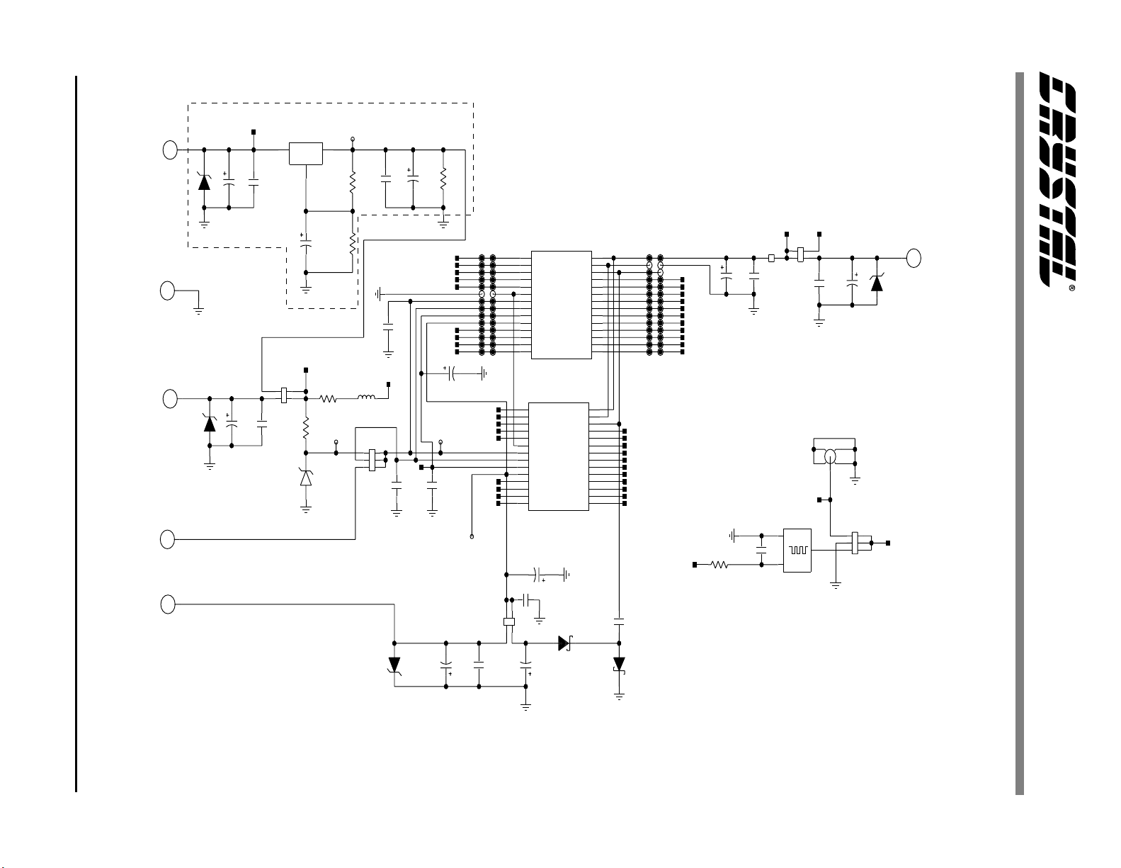
2.2.1 Analog Power Supply
Referring to Figure 1, the A+ post supplies power
to the positive analog power input pin (VA+) of the
CS5471. This post also supplies power to the
LT1004 voltage reference (D3) and the optional
+3V regulator (U5). If HDR9 is set to the “A-” setting, the A- post can supply the required negative
voltage to the VA- pin of the CS5471.
Note that the evaluation board contains the footprints and connectivity which allows the user to install a LM317 voltage regulator (U5), which can be
used to create +3 V from a +5 V supply. This option is useful if the user wants to interface the ev aluation board to another board that can only operate
from a +5V supply. With HDR17 set to “+5V_IN”,
one single +5 V supply can be used to provide both
a +5V to various microcontrollers and/or other peripheral devices, as well as +3 V for the CS5471.
The included schematic diagram shows the circuitry for the +5V regulator circuitry inside a box with
dashed lines. These components are not populated
when the board is shipped from the factory, but the
user can install these components if desired.
2.2.2 Digital Power Supply
The A+ post can be used to supply both the analog
power (to CS5471 VA+ pin) as well as the digital
power (to CS5471 VD+ pin). However if a separate supply voltage is desired for the digital power
DS480DB1 5
Page 6

CDB5471
supply, the “VD+” banana connector post can be
used to independently supply a separate digital
power supply to the input of the CS5471 (VD+
pin), the 4.096 MHz oscillator (U1), and circuitry
for the parallel port interface. This is controlled by
the setting on HDR18.
The user should note that the CS5471 can operate
with a digital supply voltage of either +3V or +5V.
ferring to Figure 1, circuitry for a charge-pump circuit is included on-board. The charge pump circuit
consists of capacitors C11, C12, and C36, and diodes D1 and D2.
As an alternative to using the charge pump circuit,
the user can supply an off-board -2V DC power
source to the “A-” banana connector. This option
is controlled by the setting on HDR9.
This voltage is defined as the voltage presented
across VD+ and DGND.
2.3 Eval Board Control - Headers/Switches
Table 2 lists the various adjustable headers and
2.2.3 Charge Pump Options
The output from CS5471’s charge-pump driver pin
(CPD) can be used to generate a -2V supply when
the proper jumper settings are selected on HDR9.
This -2V supply can be used as the negative power
supply connection for the CS5471’s VA- pin. Re-
Power Supplies Power Post Connections
Analog Digital A+ A- GND D+ +5 V_IN HDR9 HDR17 HDR18
+3 +3 +3 -2 0 +3 NC
switches on the CDB5471 Evaluation Board, as
well as their default settings (as shipped from the
factory). The header settings can be adjusted by the
user to select various options on the evaluation
board. These options are described further in the
following paragraphs.
A-
CPD
O O
O O
+5V_IN
A+
O O
O O
VD+
V+
O O
O O
+3 +3 +3 -2 0 NC NC
+3 +3 +3 NC 0 +3 NC
+3 +3 +3 NC 0 NC NC
+3 +3 NC -2 0 NC +5
+3 +3 NC NC 0 NC +5
+3 +5 +3 -2 0 +5 NC
+3 +5 +3 NC 0 +5 NC
+3 +5 NC -2 0 +5 +5
+3 +5 NC NC 0 +5 +5
+5 +3 +5 0 +2 +5 NC
Table 1. Power Supply Connections
A-
CPD
A-
CPD
A-
CPD
A-
CPD
A-
CPD
A-
CPD
A-
CPD
A-
CPD
A-
CPD
A-
CPD
O O
O O
O O
O O
O O
O O
O O
O O
O O
O O
O O
O O
O O
O O
O O
O O
O O
O O
O O
O O
+5V_IN
A+
+5V_IN
A+
+5V_IN
A+
+5V_IN
A+
+5V_IN
A+
+5V_IN
A+
+5V_IN
A+
+5V_IN
A+
+5V_IN
A+
A+
O O
O O
O O
O O
O O
O O
O O
O O
O O
O O
O O
O O
O O
O O
O O
O O
O O
O O
O O +5V_IN
O O
VD+
V+
VD+
V+
VD+
V+
VD+
V+
VD+
V+
VD+
V+
VD+
V+
VD+
V+
VD+
V+
VD+
V+
O O
O O
O O
O O
O O
O O
O O
O O
O O
O O
O O
O O
O O
O O
O O
O O
O O
O O
O O
O O
6 DS480DB1
Page 7

CDB5471
Name Function Description Default Setting Default Jumpers
HDR1
HDR2
HDR3
HDR4
HDR5
HDR6
HDR7
HDR8
HDR9
Used to switch IIN3+ on the CS5471 between J2
and AGND.
Used to switch VIN3- on the CS5471 between J3
and AGND.
Used to switch VIN3+ on the CS5471 between J1
and AGND.
Used to switch IIN3- on the CS5471 between J4
and AGND.
Used to switch VIN2- on the CS5471 between J6
and AGND.
Used to switch IIN2+ on the CS5471 between J7
and AGND.
Used to switch IIN2- on the CS5471 between J5
and AGND.
Used to switch VIN2+ on the CS5471 between J8
and AGND.
Used to switch between external VA- and on-board
CS5471 charge-pump circuit, CPD
IIN3+ Set to BNC J2
VIN3- Set to BNC J3
VIN3- Set to BNC J1
IIN3- Set to BNC J4
VIN2- Set to BNC J6
IIN2+ Set to BNC J7
IIN2+ Set to BNC J5
VIN2+ Set to BNC J8
CPD active
O O IIN3+
O O AGND
O O VIN3O O AGND
O O VIN3+
O O AGND
O O IIN3O O AGND
O O VIN2O O AGND
O O IIN2+
O O AGND
O O IIN2O O AGND
O O VIN2+
O O AGND
A-
O O
O O
CPD
HDR10
HDR11
HDR12
SW1
HDR13
HDR14
Used to switch VIN1+ on the CS5471 between J9
and AGND.
Used to switch IIN1- on the CS5471 between J12
and AGND.
Used to switch IIN1+ on the CS5471 between J10
and AGND.
S1-1 sets logic level on CS5471
GAIN input pin
S1-2 sets logic level on CS5471 OWRS input pin
Used to switch VIN1- on the CS5471 between J11
and AGND.
Used to switch the VREFIN from external VREF
post connector, to the on board LT1004 reference,
or to the on-chip reference VREFOUT. Refer to
Table 3.
VIN1+ Set to BNC J9
IIN1- Set to BNC J12
IIN1- Set to BNC J10
SW1-2 Open (GAIN=x1)
SW1-1 Open (XIN/1024
VIN1- Set to BNC J11
VREFIN Set to on-
chip reference
VREFOUT
)
O O VIN1+
O O AGND
O O IIN1O O AGND
O O IIN1+
O O AGND
23
OPEN
O O VIN1O O AGND
O O LT1004
O O VREFOUT
O O EXT VREF
Table 2. Default Header Settings
DS480DB1 7
Page 8

CDB5471
Name Function Description Default Setting Default Jumpers
HDR15 Controls the source for the CS5471 XIN clock input.
HDR16 This header should always be shorted. Short this header
Determines whether the main analog supply will be
HDR17
HDR18
2.3.1 Analog Inputs
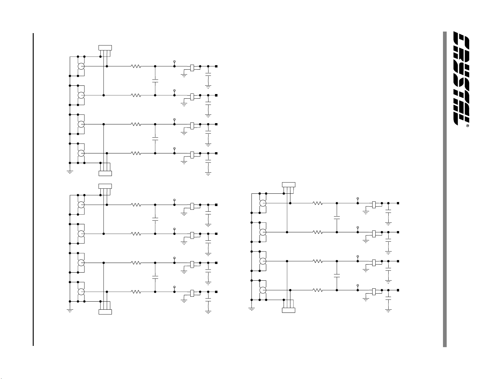
Refer to Figure 2. The settings on the 14 analog input headers (2 headers per channel) which are designated as HDR10 through HDR13, determine
which of the input lines will carry a signal, and
which input lines may be grounded. They can be
configured to accept either a single-ended or differential signal. Using the voltage channel as an example (see Figure 2), note that HDR10 sets the
input to the positive side of the first voltage channel
input (VIN1+ pin). HDR13 sets the input to the
negative side of the first voltage channel input
(VIN1- pin). In a single-ended input configuration,
HDR13 would be set to the “AGND” setting, and
HDR10 would be set to “VIN1+” and would conduct the single-ended signal. In a differential input
configuration, HDR13 would be set to “VIN1-”
and HDR10 would be set to “VIN1+” and this pair
of inputs would form the differential input pair into
the VIN1+ and VIN1- pins of the CS5471.
WARNING: DANGER! One of the possible applications for the CS5471 includes data acquisition
for a power metering system. However, the user
should not attempt to directly connect any leads
from a high-voltage power line to the evaluation
board inputs, even if the current/voltage levels are
gain reduced by resistive dividers and/or shunts.
Because the ground terminal of the parallel cable
(from the PC) is near or at earth ground potential,
powered from the A- post, or from the regulated 3V
voltage (generated from the +5V_IN) post input.
Choose whether the digital circuitry will be powered
by main analog supply, or powered by separate digital supply (through VD+ post).
Table 2. Default Header Settings (Continued)
the ground node on the evaluation board will also
be forced to earth ground potential. Serious dam-
age and even personal injury can occur if a “hot”
voltage main is connected to any point on the eval-
uation board, including the analog input connec-
tors. Such power line signals must be isolated by
current/voltage transformers and reduced in mag-
nitude before they can be safely applied to the eval-
uation board.
Several patch-circuit areas are provided near the
voltage/current input headers, in case the user
wants to connect special sensor circuitry to the an-
alog inputs (such as transformers, shunt resistors,
etc., for sensory the voltage/current on a single-
phase power line). For the input channel, a Shunt
Resistor or Current Transformer can be mounted in
these areas and connections can be made to current-
channel input pair. Likewise, the three channels, a
Voltage Divider or Voltage Transformer can be
connected to the CS5471’s voltage input pair. Note
from Figure 2 that a simple R-C network filters
each sensor’s output to reduce any interference
picked up by the input leads. The 3 dB corner of the
filter is approximately 50 kHz differential and
common mode.
Note that the CDB5471 Evaluation Board is also
used as the evaluation board for the CS5451 A/D
converter, which is a 6-channel version of the
CS5471. The user can use this board to the evalu-
Set to on-board 4.000
MHz crystal (U1).
Set to A-
Set to main analog
supply
O O EXT XIN
O O DGND
O O 4.0096 MHz
O O
O O +5V_IN
O O A+
VD+
O O
O O
V+
OSC
8 DS480DB1
Page 9
CDB5471
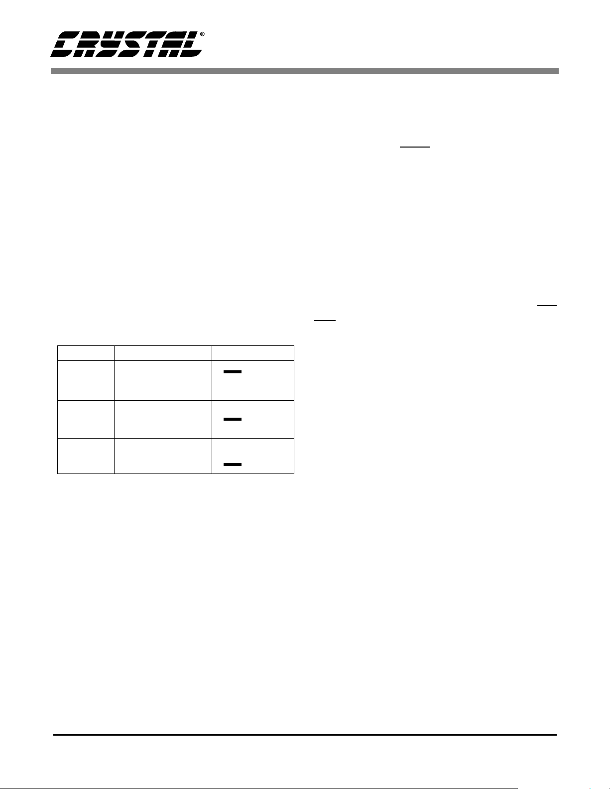
Reference Description HDR14
LT 1004
Select on board
LT1004 Reference
(5 ppm/
°C)
VREFOUT
Select reference sup-
plied from CS5471
VREFOUT pin
EXTVREF
Select external
reference
Table 3. Reference Selection
ate CS5451 by obtaining a CS5451 sample and
connect it in place of the CS5471 device. Then the
remaining four input channels serve as the inputs to
the CS5451’s four additional input pairs.
Other header options listed in Table 2 allow the
user to set the source of the input clock signal and
the source of the voltage reference (VREFIN) input, etc. The voltage reference options and clock
input options are discussed next.
2.3.2 Voltage Reference Input
To supply the CS5471 with a suitable 1.2 V voltage
reference input at the VREFIN pin, the evaluation
board provides three voltage reference options: onchip, on-board, and external. See HDR14 as shown
in Figure 1. Table 3 illustrates the available voltage
reference settings for HDR14. With HDR14’s
jumpers in position “VREFOUT,” the CS5471’s
on-chip reference provides 1.2 volts. With HDR14
set to position “LT1004,” the LT1004 provides
1.23 volts (the LT1004 temperature drift is typically 50 ppm/°C). By setting HDR14’s jumpers to position “EXT VREF,” the user can supply an
external voltage reference to J16 connector post
(VREF) and AGND inputs.
2.3.3 Clock Source for XIN
A 4.000 MHz crystal is provided to drive the XIN
input of the CS5471. (See Figure 1.) However, the
user has the option to provide an external oscillator
signal for XIN, by switching the setting of HDR15.
O O LT1004
O O VREFOUT
O O EXT VREF
O O LT1004
O O VREFOUT
O O EXT VREF
O O LT1004
O O VREFOUT
O O EXT VREF
2.3.4 S1 DIP Switch
Referring to Figure 3, the two single-pole singlethrow switches on SW1 DIP switch should be used
to control the logic settings on the CS5471’s
OWRS pin and GAIN pin. When these SW1
switches are set to “OPEN” the corresponding pin
on CS5471 is set to D+ potential, which creates a
logic-high state. When the user closes either of
these SW1 switches, the corresponding pin on
CS5471 is grounded, which creates a logic-low
state on the pin.
2.3.5 Reset Circuit
Circuitry has been provided which allows the user
to execute a hardware reset on the CS5471. (See
Figure 3). By pressing on the S1 switch, the RESET pin on the CS5471 will be held low until the
switch is released.
2.3.6 External Signal In/Out Header
Note that HDR16 is included on the CDB5471
Evaluation Board as a header that is normally left
unconnected. This header provides a way for the
user to interface the CDB5471 Evaluation Board to
other prototype boards, calibrators, logic analyzers,
other peripherals, etc. in order to further evaluate
the CS5471 device and/or to use the evaluation
board as a platform for the prototype development
of a digital power metering solution. However,
note that the CDB5471 Evaluation Board is not intended to be integrated directly into a commercial
digital power meter. The layout of the board is not
optimized for practical power metering situations.
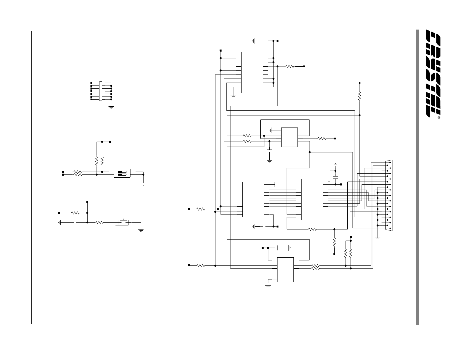
2.3.7 Serial-to-Parallel Interface
Glue-logic on the evaluation board converts the
CS5471 serial data into 8-bit segments (bytes).
The bytes are sent to the DB25 connector (J17), and
then through the standard printer cable to the user’s
PC. This section briefly describes the operation of
the digital circuitry on the CDB5471 that provides
the 8-bit parallel data to the PC. Refer to Figure 3.
DS480DB1 9
Page 10

CDB5471
The user should recall from CS5471 Data Sheet
that the serial interface on the CS5471 device is a
“master-mode” interface, which means tha t the device provides the clock. Once the CS5471 is powered on, the SCLK pin produces a clock signal, and
data is sent out on the SDO pin of the device. When
the evaluation software is instructed (by the user) to
acquire data through the parallel interface, a twostep process is performed: Firs t the software synchronizes itself to the frame rate of the CS5471,
then the software acquires multiple frames of data
from the CS5471.
2.3.7.1. Synchronization
When the software is commanded to acquire data,
the software will first synchronize itself to the
frame rate of the CS5471 (see CS5471 Data Sheet).
This is done by measuring the amount of time between rising and falling edges of the “BUSY” signal. (BUSY will change state every time the
CS5471 issues eight SCLKs--See next section for a
more detailed description.) By measuring this time
period, the software can determine the idle period
of the frame, which allows it to be prepared to collect a complete frame’s worth of data when the next
CS5471 frame is received. This acquisition sequence is described next.
After sixteen SCLKs, the PC software has acquired
two bytes (16 bits) which represents one data sam-
ple. The 4-bit up/down counter (U6) will roll over
after every 16 SCLKs. (Note that U6 is cleared by
the CS5471’s FSO signal at the beginning of each
frame, which insures that the counter begins the
frame in the correct state--cleared). This sequence,
which lasts for 16 SCLKs, is performed a total of
six times, although only the first two repetitions of
this sequence are relevant. In the first two sequenc-
es, the two 16-bit words from the CS5471 are ac-
quired by the PC. The data contained in the
remaining four sequence executions will be mean-
ingless, as the state of the CS5471’s SDO pin is be
undefined during the last 64 clocks of each data
frame.
After the sixth 16-bit word is acquired, the software
recognizes that the end of a data frame has been
reached, and it will continue to wait for the next
transition on the “BUSY” line. This will not oc cur
until the first 8 SCLKs of the next frame are sent
from the CS5471. Various other signals in Figure
3 (STRB, FEED, ACK, etc.) are not used during
data capture and are only used for testing (internal
use only).
2.3.8 Connecting the Eval Board to PC
2.3.7.2. Acquisition
Referring to Figure 3, the CS5471’s SCLK line is
used to clock the 8-bit serial-in/parallel-out shiftregister (U7) which accepts the serial data on SDO
and shifts it into the 8 output bits QA-QG. The
SCLK signal is also fed into the up/down counter
U6 and after every 8 SCLKs, the “QC” pin of U6
will latch the QA-QG output bits of U6 into the 8bit D-Flip-Flop (U3). While this is happening, the
software monitors the “BUSY” signal (from the
“QD” pin of U6). BUSY is the critical handshake
signal. A rising or falling transition on BUSY indicates to the software that it is now time t o coll ec t
another byte of data from the latched output on U3.
10 DS480DB1
The CDB5471 connects to the user’s IBM-compat-
ible PC with the included 25-pin parallel port cable.
The user should not connect this cable between
the CDB5471 and the parallel port on the PC until
all of the header options in Table 2 have been set
to appropriate settings and the user has applied
power to the CDB5471. The parallel cable at-
tached to the CDB5471 Evaluation Board at J17.
After connecting the parallel port cable between
the PC and CDB5471, the user should always actu-
ate (press down on) the “RESET” switch (S1) at
least one time before performing any other evalua-
tion activities.
Page 11
DS480DB1 11
+5V_IN
EXT VREF
A-
CON_BANANA
J21
P6KE6V8P
CON_BANANA
J18
CON_BANANA
A+
J14
P6KE6V8P
CON_BANANA
J16
CON_BANANA
J15
+5V
Z4
C42
10UF
GND
Do Not Populate
GND
Z2
GND
C13
47UF
C39
.1UF
C17
.1UF
3
HDR17
HDR2X2
D3
LT1004
U5
LM317LZ
IN
ADJ
1
C38
.33UF
TANT
GND
+3V
43
21
GND
OUT
R3
4.99K
TP40
2
3
TP1
TP40
TP77
2
100
R31
140
R30
10R2
FERRITE_BEAD
1.2V
3.0V
GND
L1
HDR3X2
HDR14
21
43
65
GND
V+
C40
.1UF
C20
.1UF
GND
C41
22UF
+3V
C19
.1UF
Z1
P6KE6V8P
C37
TP40
TP76
C16
.1UF
GND
1K
R29
GND
SCLK
SDO
FSO
/GAIN
VIN3+
VIN3-
IN3+
IN3-
SE
TP38 TP39
TP40 TP41
TP42 TP43
TP44 TP45
TP46 TP47
TP48 TP49
TP50 TP51
TP52 TP53
TP54 TP55
TP56 TP57
TP58 TP59
TP60 TP61
TP62 TP63
4.7UF
TANT
SCLK
SDO
FSO
/GAIN
VIN3+
VIN3-
IN3+
IN3-
TP2
TP40
C15
47UF
C1
.1UF
D+ V+
HDR18
HDR1X2
C14
.1UF
HDR16
HDR2X2
21
21
43
C22
C23
47UF
.1UF
GND
U4
/RESET
28
VD+
27
DGND
26
CPD
25
XIN
24
23
OWRS
22
VIN1+
21
VIN1-
20
IIN1+
19
IIN1-
18
VIN2+
17
VIN2-
16
IIN2+
1514
IIN2-
TP78TP79
TP73
TP72
TP74 TP75
TP14 TP15
TP16TP17
TP18TP19
TP20TP21
TP22TP23
TP24TP25
TP26TP27
TP28TP29
TP30TP31
TP32TP33
TP34TP35
XIN
/RESET
OWRS
VIN1+
VIN1IIN1+
IIN1VIN2+
VIN2IIN2+
IIN2-
C21
10UF
GND
1
TP37TP36
SCLK
2
SDO
3
FSO
4
SE
5
/GAIN
6
AGND
7
VREFIN
8
VREFOUT
9
VA+
10
VA-
11
VIN3+
12
VIN3-
13
IN3+
IN3-
CON_BANANA
J20
Z3
P6KE6V8P
VD+
SSOP28_200_P65MM
GND
U2
GND
D2
BAT85
/RESET
28
VD+
27
DGND
26
CPD
25
XIN
OWRS
VIN1+
VIN1IIN1+
IIN1VIN2+
VIN2IIN2+
IIN2-
XIN
24
/RESET
23
OWRS
22
VIN1+
21
VIN1-
20
IIN1+
19
IIN1-
18
VIN2+
17
VIN2-
16
IIN2+
1514
IIN2-
C18
.1UF
4.0960MHZ
7
14
GND
D+
10R32
GND
VCC
EXT_IN
J13
BNC_RA
GND
HDR3X2
HDR15
12
34
XIN
8
56
U1
GND
C11
.039UF
D1
BAT85
1
SCLK
2
SDO
3
FSO
4
SE
SE
5
/GAIN
6
AGND
7
VREFIN
8
VREFOUT
9
VA+
10
VA-
11
VIN3+
12
VIN3-
13
IN3+
IN3-
SKT_SSOP28_ENP
TANT
4.7UF
C36
.1UFC2
43
21
HDR9
GND
HDR2X2
TANT
2.2UF
C12
CDB5471
GND
GND
Figure 1. Power Supply, CS5471, and Os cillator
Page 12
12 DS480DB1
J22
432
1
TP67
HDR2X2
GND
GND
GND
GND
GND
GND
GND
GND
HDR7
21
43
HDR2X2
HDR6
12
34
HDR2X2
HDR5
12
34
HDR2X2
HDR8
21
43
HDR2X2
HDR11
12
34
HDR2X2
HDR12
21
43
HDR2X2
HDR13
21
43
HDR2X2
HDR10
12
34
GND
GND
GND
GND
GND
GND
GND
GND
C24
.01UF
C25
.01UF
C26
.01UF
C27
.01UF
C28
.01UF
C29
.01UF
C30
.01UF
C31
.01UF
IIN2-
IIN2+
VIN2-
VIN2+
IIN1-
IIN1+
VIN1-
VIN1+
GND
J1
BNC_RA
J3
BNC_RA
J2
BNC_RA
J4
BNC_RA
J24
123
4
J27
123
4
R19 301
0.1%
R18 301
0.1%
301R17
0.1%
301R20
0.1%
C6
4700PF
C5
4700PF
TP71
TP70
TP69
TP68
GND
GND
GND
GND
HDR2X2
HDR3
12
34
HDR2X2
HDR2
21
43
HDR2X2
HDR1
21
43
HDR2X2
HDR4
12
34
GND
GND
GND
GND
C32
.01UF
C33
.01UF
C34
.01UF
C35
.01UF
VIN3+
VIN3-
IN3+
IN3-
CDB5471
GND
GND
J5
BNC_RA
J7
BNC_RA
J6
BNC_RA
J8
BNC_RA
J12
BNC_RA
J10
BNC_RA
J11
BNC_RA
J9
BNC_RA
123
4
1
J26
4
123
432
R21 301
R24 301
J25
J23
R28 301
R25 301
301R23
0.1%
301R22
0.1%
0.1%
0.1%
301R26
0.1%
301R27
0.1%
0.1%
0.1%
C8
4700PF
C7
4700PF
C9
4700PF
C10
4700PF
TP66
TP65
TP64
TP4
TP5
TP6
TP3
Figure 2. Analog Inputs
Page 13
DS480DB1 13
OWRS
/RESET
/GAIN
SCLK
FSO
SDO
GND
.1UFC43
D+
D+
HDR7X2
HDR19
21
43
65
87
SE
109
1211
1413
GND
GND
1
DATA B
2
3
QA
4
CD
5
CU
6
QC
7
QD
8
GND
MM74HC193N
U6
16
VCC
DATA A
BORROW
CARRY
LOAD
DATA C
DATA D
15
R8
14
CLR
13
12
11
10
9
470
FSO
D+
QB
10KR6
BUSY
INIT
/GAIN
OWRS
D+
GND
R35 10K
R34 10K
R36
.1UFC46
20K
/RESET
R37
10KR33
R16 10K
49.9
D+
SW1
2
1
SW_DIP_2
S1
SW_B3W_1100
OPEN
GND
GND
SDO
SCLK
R10
R11
470
470
R15
2
1
8
9
R7
4.7K
470
SN74HC164N
B
A
CLK
/CLR
U7
GND
GND
VCC
D+
QG
QF
QE
QD
QC
QB
QA
.1UFC3
GND
GND
19
11 9
13
15
17
C45
220PF
COG
GND
7
13
12
11
10
6
5
4
3
14
20
VCC 1/G
18
1Y1
16
1Y2
14
1Y3
12
1Y4
10
GND
SN74HC240N
U8
2/G
2A1
2A2
2A3
2A4
SN74HC240N
GND
D+
C44.1UF
U8
1A1
1A2
1A3
1A4
2Y1
2Y2
2Y3
2Y4
GND
7
5
3
SN74HC374N
8D
18
7D
17
14
5D
13
4D
8
3D
7
2D
4
1D
3
CLK
11
/OC
1
R13
1
2
4
6
8
R9
470
SE
ACK
DB25M_RA
J17
GND
1
14
2
15
3
16
4
17
5
18
6
19
7
20
8
21
9
22
10
23
11
24
12
25
13
GND
.1UF
GND
VCC
8Q
7Q
6Q6D
5Q
4Q
3Q
2Q
1Q
U3
4.7K
C4
10
D+
20
19
16
15
12
9
6
5
2
SEL
D+
10KR1
10KR5
10KR4
D+
STRB
4.7KR12
4.7KR14
FEED
CDB5471
Figure 3. Digital Circuitry
Page 14

CDB5471
3. SOFTWARE
The evaluation software was developed with La b
Windows/CVI, a software development package
from National Instruments. The software is designed to run under Windows 95 or later, and requires about 3 MB of hard drive space (2 MB for
the CVI Run-Time Engine, and 1 MB for the evaluation software). After installing the software, read
the readme.txt file for any last minute updates or
changes. More sophisticated analysis software can
be developed by purchasing the development package from National Instruments (512-794-0100).
3.1 Installing the Software
Installation Procedure:
1) Turn on the PC, running Windows 95 or later.
2) Insert the Installation Diskette #1 into the PC.
3) Select the Run option from the Start menu.
4) At the prompt, type: A:\SETUP.EXE <enter>.
5) The program will begin installation.
6) If it has not already been installed on the PC,
the user will be prompted to enter the directory
in which to install the LabWindows CVI RunTime Engine. The Run-Time Engine manages executables created with Lab Windows/CVI. If the default directory is
acceptable, select OK and the Run-Time Engine will be installed there.
7) After the Run-Time Engine is installed, the
user is prompted to enter the directory in which
to install the CDB5471 software. Select OK to
accept the default directory.
8) Once the program is installed, it can be run by
double clicking on the EVAL5451 icon, or
through the Start menu.
Note: The software is written to run with 640 x 480
resolution; however, it will work with 1024 x 768
resolution. If the user interface seems to be a little
small, the user might consider set ting the
display settings to 640 x 480. (640x480 was
chosen to accommodate a variety of
computers).
3.2 Running the Software
3.2.1 Getting Started
The CDB5471 Evaluation software allows the user
to obtain, display, and save data that is acquired by
the CS5471 chip. Before running the software, the
first step is to make sure that all of the headers that
are listed in Table 2 are set to an appropriate setting, the exact setting should be determined by the
user. Next, with the user’s DC power supplies still
turned off, the user should connect the necessary
power leads to the banana jack power conne ctors
on the evaluation board. Refer to Table 1 for various acceptable power supply connection configurations. Then at this time the user should turn on their
DC power supplies, which should apply power to
the CDB5471. Several test point locations are
available on the evaluation board. The user can
check these test points with a voltmeter, to make
sure that the voltages at these test points are at the
expected levels. When the user has verified that the
power supply levels are constant, the user should
connect the included 25-pin cable between J17 of
the evaluation board and the parallel port on the user’s PC. The user should then press down on the S1
“RESET” switch, and make sure to hold it down for
at least ~0.5 seconds before releasing. Finally, the
user can start the PC software. To start the software, double click on the EVAL5451 icon, or initiate through the Start menu.
14 DS480DB1
Page 15
CDB5471
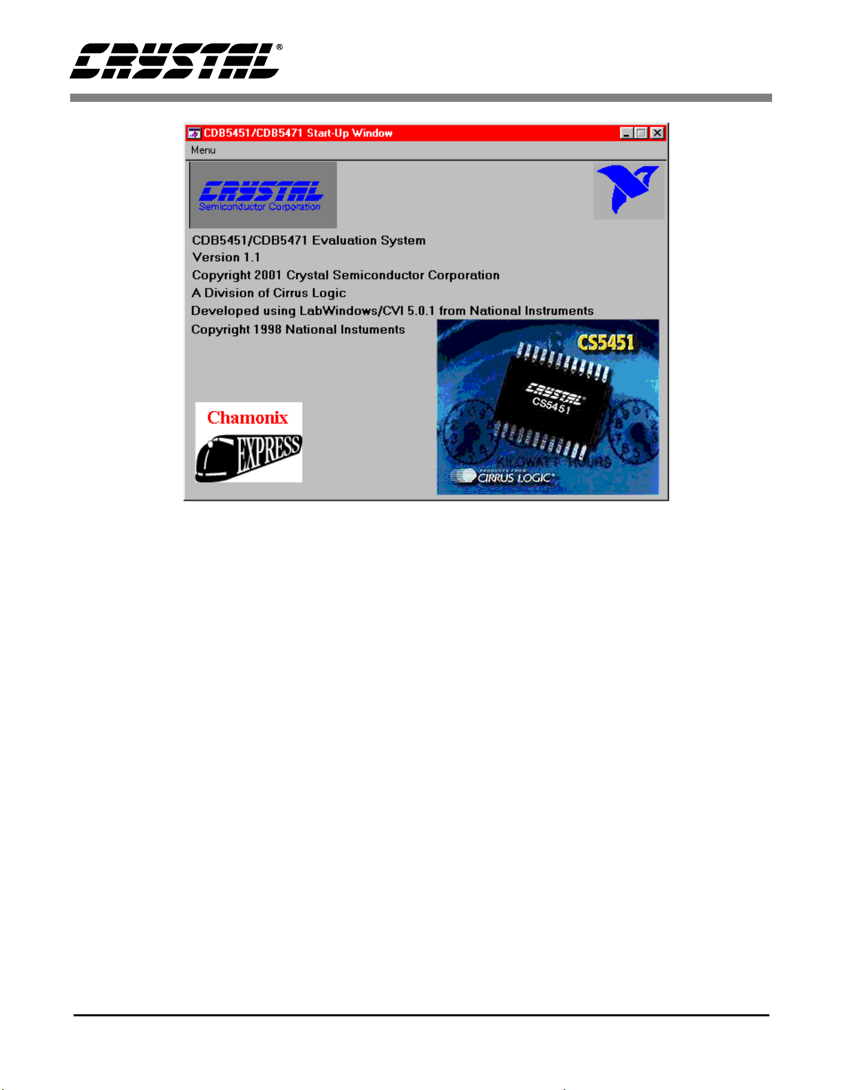
Figure 4. Start-Up Window
3.2.2 The Start-Up Window
When the software first executes, the user should
see the Start-Up Window appear on the user’s PC
monitor. This window is shown in Figure 4. From
this window, the user can navigate to three other
main windows: the Conversion Window, the Data
Collection Window, and CS5471 Pinout Diagram.
(The CS5451 Pinout Diagram is also included in a
fourth window.) To navigate to these windows, use
the mouse to click on the “Menu” item, which is located towards the upper left cor ner of the Star t-Up
Window. “Menu” is a pull-down menu which contains four options. From this pull-down menu, the
user can select any of the three windows mentioned
above, and once this is done, the new window
should appear. A fourth option called “Exit”
should be selected when the user wants to terminate
execution of the evaluation board software program.
If the user selects the “CS5471 Pinout Diagram”
option in the “Menu” pull-down, the software will
display a window which contains the pin diagram
of the CS5471. This pin diagram is included for the
user’s reference. Note that this window has no actual functionality.
The functionality of the Conversion Window and
the Data Collection Window is described next.
3.2.3 The Conversion Window
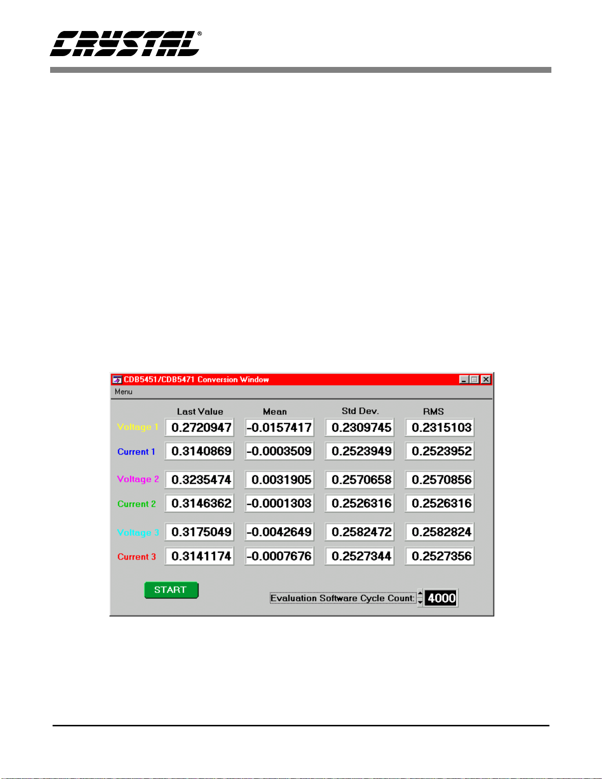
Refer to Figure 5. After the user presses on the
green-colored “START” button in this window, the
software will begin to collect data for bo th channels
of the CS5471. For each channel, a certain number
of instantaneous data samples from the CS5471 are
bundled together. The period over which each bundle of samples is taken is called a “computation cycle.” The user controls the number of
instantaneous data samples that will be taken (per
channel) during one computation cycle by adjusting the number in the box labeled “Evaluation Software Cycle Count:.” Note that the default value for
this is set to 4000. Thus during every computation
cycle, the PC software will acquire 4000 samples
DS480DB1 15
Page 16
CDB5471
(from both channels) and it will update the onscreen results of both channels after calculating the
results on each successive set of 4000 samples.
The results that are displayed on this screen are
therefore updated after each computation cycle.
Note that the results in the very first computation
cycle (after the “START” button has been activated) will not be valid. Accuracy of the Mean, Std.
Dev. and RMS results will increase as the “Samples to Average” value is increased.
The user should understand how to interpret the
values that are displayed in the array of number
boxes in the Conversion Window. For CDB5471,
only the results displayed in the “Voltage 1” and
“Current 1” rows are valid. The result values
that are displayed in these numeric output boxes are
all expressed on a normalized scale. The highest
value (0.999...) represents the highest digital output
code that can be issued from the CS5471 (which is
+32767), while the lowest value -0.999... represents the most negative output code that can be issued from the CS5471 (which is -32768). This is
because the CS5471 issues instantaneous output
codes as two’s complement 16-bit words. Therefore, the range of values that can be returned from
the CS5471 are between -32768 and +32767. The
CS5471 issues instantaneous data, and every computation cycle, the software computes/displays the
quantities which are described below:
Figure 5. Conversion Window
16 DS480DB1
Page 17
CDB5471
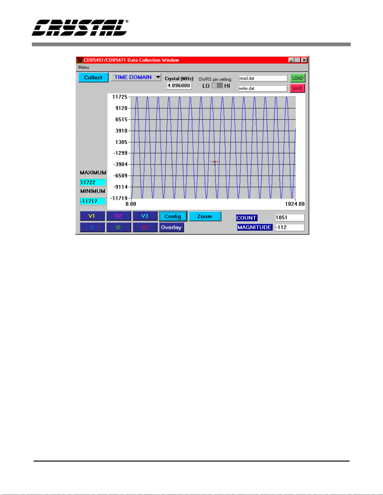
Figure 6. Data Collection Window (Time Domain)
3.2.3.1. Last Value
The first column is labelled as “Last Value.” The
value in this box represents the value of the very
last instantaneous sample that was taken (for both
channels) in the most recently-completed computation cycle. If the user’s analog input waveforms are
AC in nature, then this column of results will rarely
have any meaning. But if the user applies a constant DC input signal to any of the analog input
channels, then the Last Value co lumn for that channel should display an output code that is relatively
constant from one conversion cycle to the next.
3.2.3.2. Mean
The values in th is co lu mn r epr esen t th e simple a vera ge
of the sample valu e s in th e lat est computation cycle.
3.2.3.3. Std Dev.
The values in this column represent the computed
standard deviation over the set of values in the most
recent computation cycle.
3.2.3.4. RMS
The values in this column represent the computed
RMS value over the most recently-completed computation cycle.
3.2.4 Data Collection Window
The Data Collection Window (Figs 6, 8, and 9) allows the user to collect samples sets of data from
CS5471 and analyze them using time domain, FFT,
and histogram plots. The Data Collection Window
is accessible through the Menu option, or by pressing F4.
3.2.4.1. Collect Button
This button will collect data from the CS5471, to be
analyzed in the plot area. See the se ction on Collecting Data Sets for more information.
DS480DB1 17
Page 18

CDB5471
3.2.4.2. Time Domain / FFT / Histogram
Selector
This selector button is located just to the right of the
Collect Button. The label on this button will
change as the user selects which analysis is to be
performed (“Time Domain” or “FFT” or “Histogram”). When the software is first started, the default mode on this selector button is Time Domain.
This user should click on this butt on to select which
type of data processing to perform on the collected
data and display in the plot area. Refer to the section on Analyzing Data for more information.
3.2.4.3. “Crystal” Value Indicator Box
The value in this box reflects the frequency of the
CS5451’s clock input (at the XIN pin). Since the
XIN frequency affects the sampling rate (the output
word rate) of the CS5451, this information must be
specified to the software so that it can accurately
depict the frequency-content of the sampled data
(in Hz) when performing an FFT analysis. The
user can enter the crystal frequency that is used on
the CDB5451 board into this box. The default value of this box is set for the on-board 4.096MHz oscillator.
3.2.4.4. OWRS Pin Setting:
This switch should be adjusted whenever the user
toggles the S1-1 DIP switch (on the evaluation
board). The default setting of this switch is HI, corresponding to the default setting on S1-1 (default
setting is “OPEN”). S1-1 drives the CS5471’s
OWRS pin to logic “1”. A logic “1” on OWRS sets
the sampling frequency of both CS5471 input
channels to XIN/1024. To toggle the state of the
on-screen switch, simply click on the switch with
the mouse.
3.2.4.5. Config Button
This button will bring up the configuration window
(shown in Fig 7) in which the user can modify the
data collection specifications. See the discussion
of the Config Window in this document.
3.2.4.6. Save Button
The red-colored SAVE button will save the data in
the current plot to a file. The exact path and filename can be specified by the user in the text window
located just to the left of the SAVE button. The
data collected for both channels will be saved to a
text file.
3.2.4.7. Load Button
The green colored LOAD button will load any data
file that was previously generated by clicking on
the red SAVE button. The exact path and filename
must be specified by the user in the text window located just to the left of the LOAD button.
3.2.4.8. Channel Selector Buttons
Clicking on buttons labeled as “V1” and “I1” will
display a certain channel of data. “V1” refers to the
voltage data taken across the Vin1+/Vin1- pins of
the CS5471. In a similar manner, clicking on the
“I1” button will display the data representing the
voltage level across the current channel input pins
(Iin1+/Iin1-).
3.2.5 Config Window
See Figure 7. Clicking on the Config button will
bring up a small pop-up window called the Config
Window. The Config Window allows the user to
set up the data collection and analysis parameters,
which are described next.
3.2.5.1. Number of Samples
This box allows the user to select the number of
samples to collect. The user can choose any wholenumber power of 2 between 16 and 32768.
3.2.5.2. Average
When performing FFT processing, this box will determine the number of FFTs to average. FFTs will
then be collected and averaged when the user clicks
on the Collect Button.
18 DS480DB1
Page 19
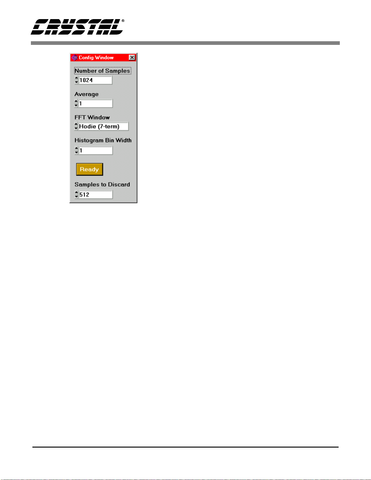
Figure 7. Configu r ation Window
3.2.5.3. FFT Window
This box allows the user to select the type of windowing algorithm for FFT processing. Windowing
algorithms include the Blackman, Black-Harris,
Hanning, 5-term Hodie, and 7-term Hodie. The 5term Hodie and 7-term Hodie are windowing algorithms developed at Cirrus Logic.
3.2.5.4. Histogram Bin Width
This box allows for a variable “bin width” when
plotting histograms of the collected data. Each vertical bar in the histogram plot will contain the number of output codes contained in this box.
Increasing this number may allow the user to view
histograms with larger input ranges.
CDB5471
all six channels). The number of samples that are
actually saved is equal to the number specified in
the Number of Samples box.
3.2.5.6. Ready Button
After the user has adjusted the parameters in the
Config Window to the desired settings, the user
must click on the READY button to close the Config Window and return to the Data Collection Window.
3.2.6 Analyzing Data
The evaluation software provides three types of
analysis tests - Time Domain, Frequency Domain,
and Histogram. The Time Domain analysis processes acquired conversions to produce a plot of
Output Code versus Conversion Sample Number.
The Frequency Domain analysis processes acquired conversions to produce a magnitude versus
frequency plot using the Fast-Fourier transform
(results up to Fs/2 are calculated and displayed).
The Histogram analysis test processes acquired
conversions to produce a histogram plot. Statistical
noise calculated are also calculated and displayed.
3.2.7 Time Domain Information
The following controls and indicators are associated with the Time Domain Analysis. Time domain
data can be plotted in the Data Collection Window
by setting the Time Domain / FFT / Histogram selector to “Time Domain.”
3.2.7.1. Count
Displays current x-position of the cursor on the
time domain display.
3.2.5.5. Samples to Discard
This number represents the number of CS5471
sample periods that will be ignored before the software starts to collect samples (when the user presses on the Collect Button). After the software has
skipped over this many data samples, the software
will then begin to save samples from the device (for
DS480DB1 19
3.2.7.2. Magnitude
Displays current y-value of the cursor on the time
domain display.
3.2.7.3. Maximum
Indicator for the maximum value of the collected
data set.
Page 20
CDB5471
3.2.7.4. Minimum
Indicator for the minimum value of the collected
data set.
3.2.8 Frequency Domain Information
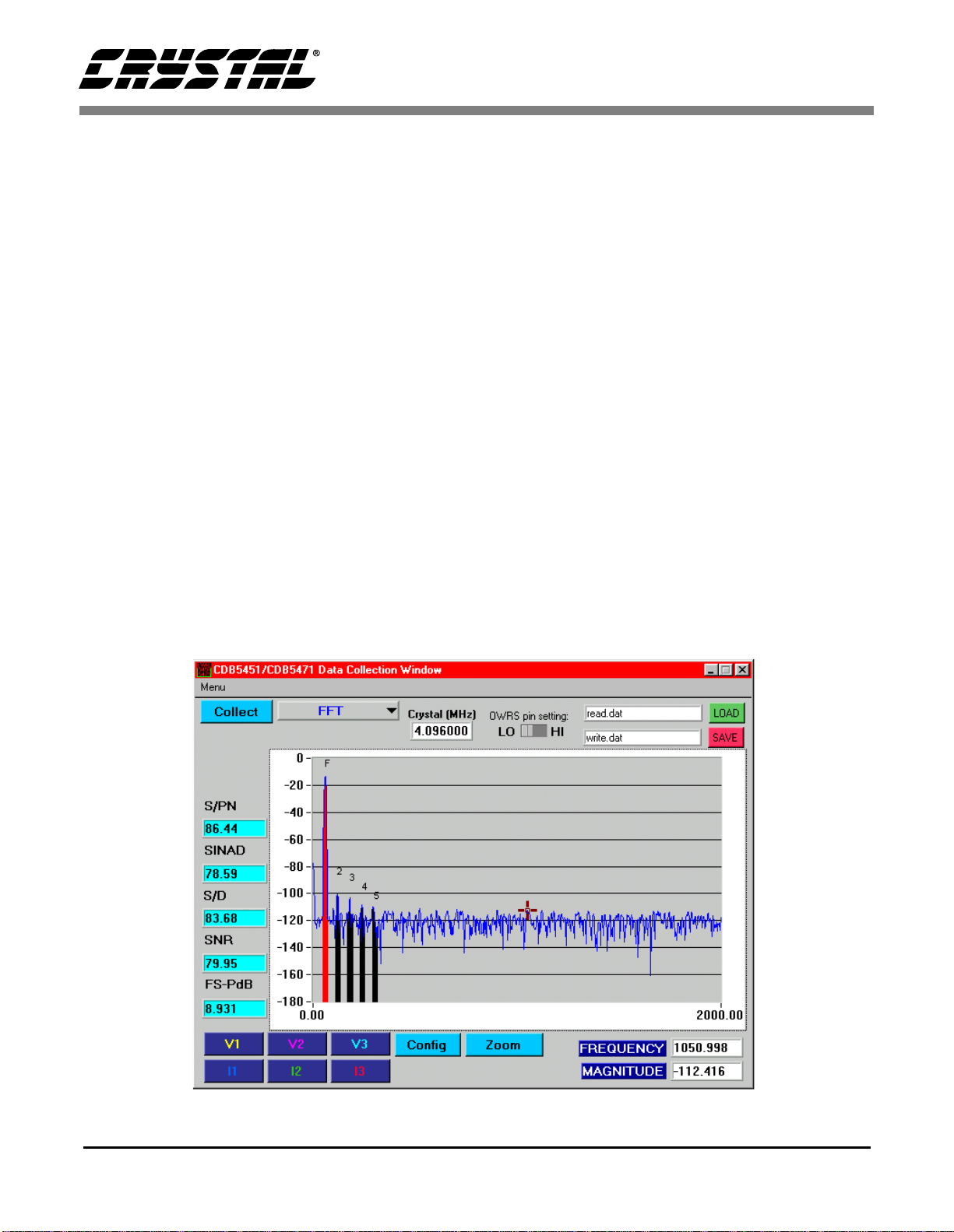
The following section describes the indicators associated with FFT (Fast-Fourier Transform) analysis. Refer to Figure 8. FFT data can be plotted in
the Data Collection Window by setting the Time
Domain / FFT / Histogram selector button to
“FFT.”
3.2.8.1. Frequency
Displays the x-axis value of the cursor on the FFT
display.
3.2.8.2. Magnitude
Displays the y-axis value of the cursor on the FFT
display.
3.2.8.3. S/D
Indicator for the Signal-to-Distortion Ratio, 4 harmonics are used in the calculations (decibels).
3.2.8.4. SINAD
Indicator for the Signal-to-Noise + Distortion Ratio
(decibels).
3.2.8.5. SNR
Indicator for the Signal-to-Noise Ratio, first 4 harmonics are note included (decibels).
3.2.8.6. S/PN
Indicator for the Signal-to-Peak Noise Ratio (decibels).
3.2.8.7. FS-PdB
Not using windowing, how far down from zero the
peak voltage input value is (decibels).
Figure 8. Data Collection Window (FFT)
20 DS480DB1
Page 21
CDB5471
3.2.9 Histogram Information
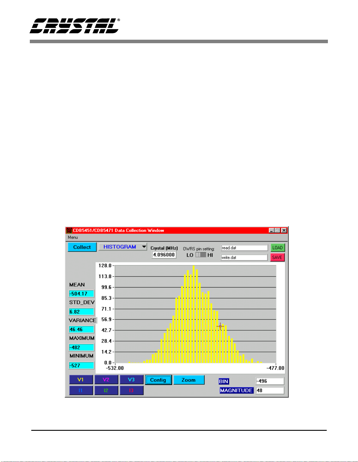
See figure 9. The following is a description of the
indicators associated with Histogram Analysis.
Histogram can plotted in the Data Collection Window by setting the Time Domain / FFT / Hist ogram
selector to “Histogram.”
3.2.9.1. Bin
Displays the x-axis value of the cursor on the Histogram.
3.2.9.2. Magnitude
Indicator for the maximum value of the collected
data set.
3.2.9.3. Mean
Average value of the collected data set.
3.2.9.4. Variance
Indicator for the calculated variance of the collected data set.
3.2.9.5. STD_DEV
Indicator for the calculated standard deviation of
the collected data set.
3.2.9.6. Maximum
Indicator for the maximum value of the collected
data set.
3.2.9.7. Minimum
Indicator for the minimum value collected in the
data set.
Figure 9. Data Collection Window (Histogram)
DS480DB1 21
Page 22
CDB5471
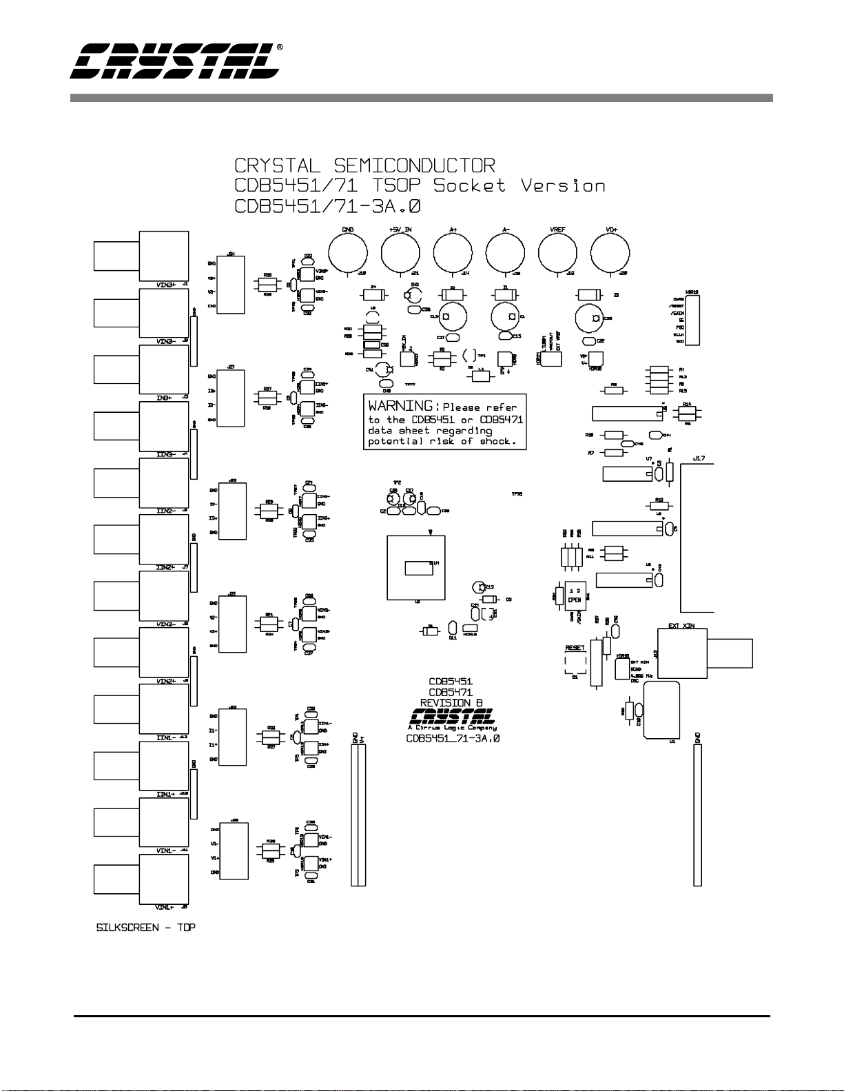
Figure 10. Silkscreen
22 DS480DB1
Page 23
CDB5471
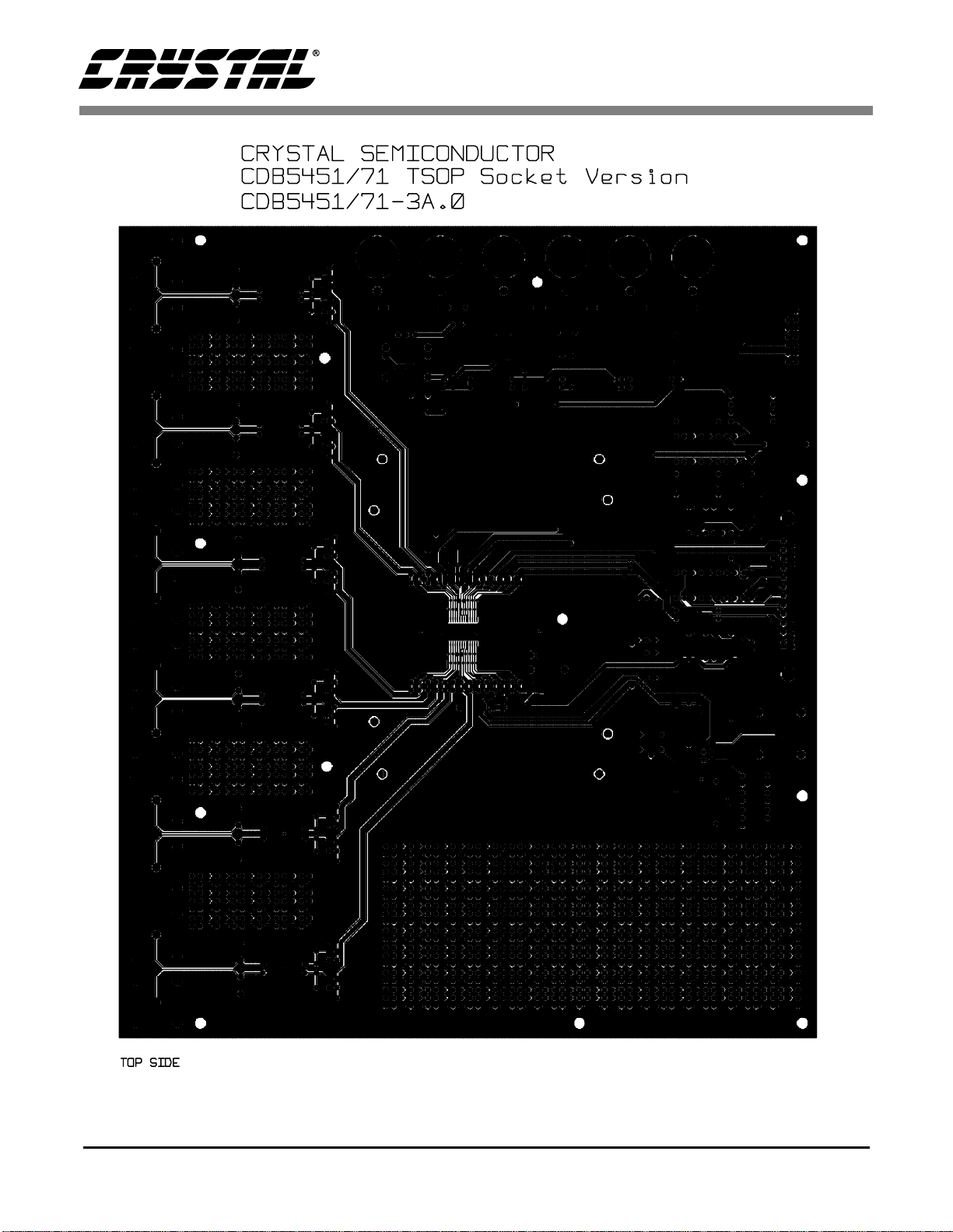
Figure 11. Circuit Side
DS480DB1 23
Page 24
CDB5471
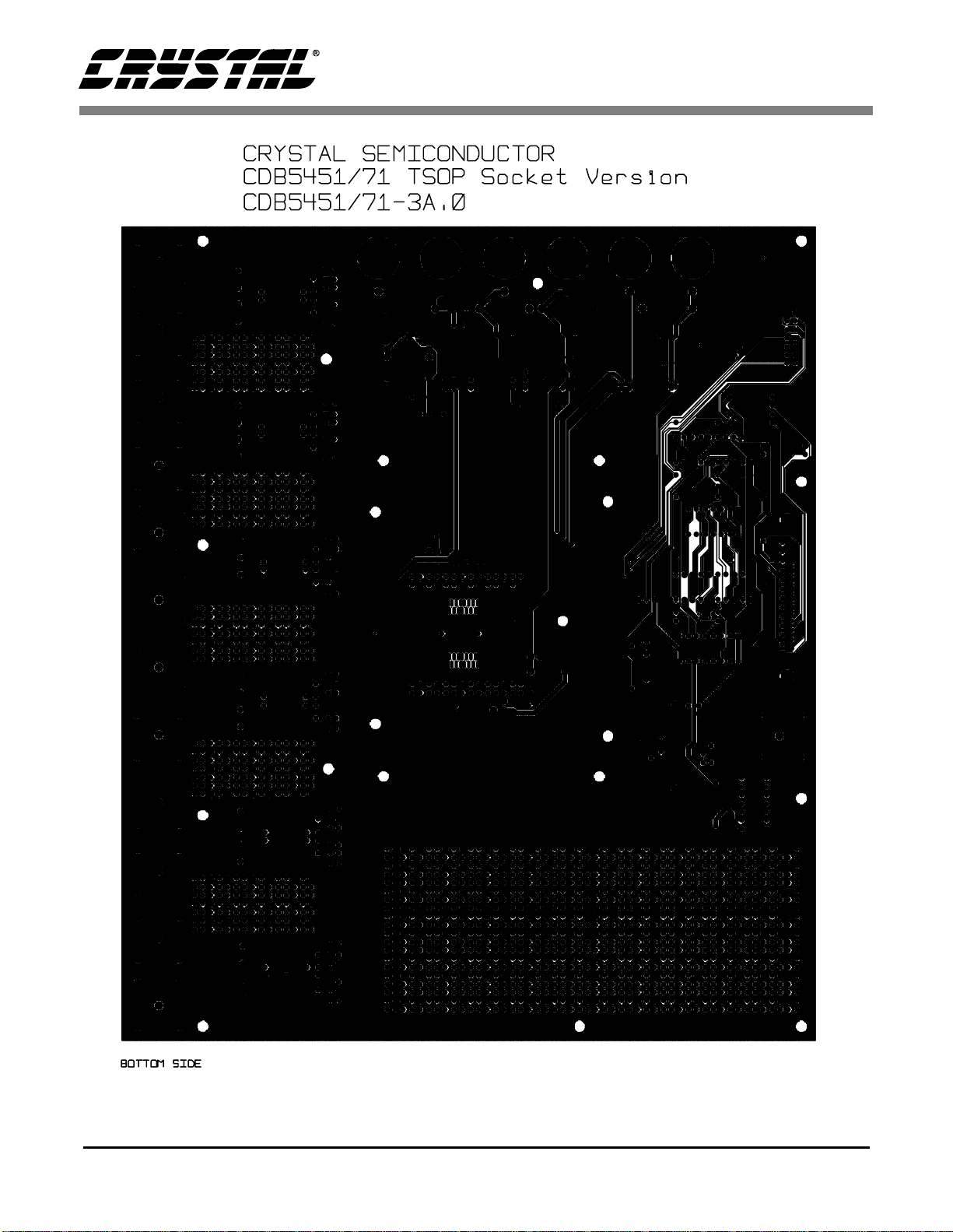
Figure 12. Solder Side
24 DS480DB1
Page 25

• Notes •
Page 26

 Loading...