

Crown MARCO-TECH 5000VZ User Manual
Notes
MACRO-TECH 5000VZ
OVERVIEW
At
first glance
the
MA-5000VZ
looks a great deal
Hke any
other
MA
Series
amplifier, except that
¡t is
physically larger
and
puts
out
more
power.
The
internal
structure
of the
MA-5000VZ
is,
however, quite
different
from
other models
in the MA
une.
To the
user, this
one is
like
the
others,
but
with a f
ew
more f eatures.
To the
technician,
this
amplifier
representsaradicaldeparturefromthe"normal"Crowndesign.
Previous
chapters covered
the
"normal," this chapter
shall
endeavorto
take
the
MA-5000VZ
as a
unique
entrty.
The
amplifier
¡s
protected
from
all
common hazards that plague high-
power
amplifiers, including
shorted,
open
or
mismatched
loads,
overloaded power
supplies,
excessive temperature,
chain-destruction
phenomena,
input-overload
damage,
and
high-frequency blowups.
The
unit
protects
loudspeakers
from
DC in the
input
signal
and
from
turn-on
and
turn-off
transients.
It
also
detects
and
prevenís
unwanted
DC
on the
outputs. Additional protection features include input current
sense,
overvoltage
(AC
mains).
A
mode
of
protection which
may
be
switched
on or
off
is
called
Loudspeaker Offset Integration (LOI).
The
LOI
circuit, when switched
on,
prevenís
excessive bass frequency
cone
excursions
below
the
audible frequency range.
It
operates essentially
as a
band-pass filter.
The
low
frequencies
are
rolled
off at
18dB/oclave
with a -3dB
córner
of
35
Hz
(Butterworth
response).
Ullra-sonics
are
rolled
off
wilh a second
order
Bessel
response
and
-3dB córner
of
SOkHz.
A
compression
circuil
in
each channel
may be
switched
off,
on
slow,
or
on
fast
by
swilches
on
Ihe
rear panel. This compressor
is
aclivaled
by
eilherinputoverloadord¡stort¡on(cl¡pping).
Compression ratio
is
infinite
(operates
as a
peak
limiter).
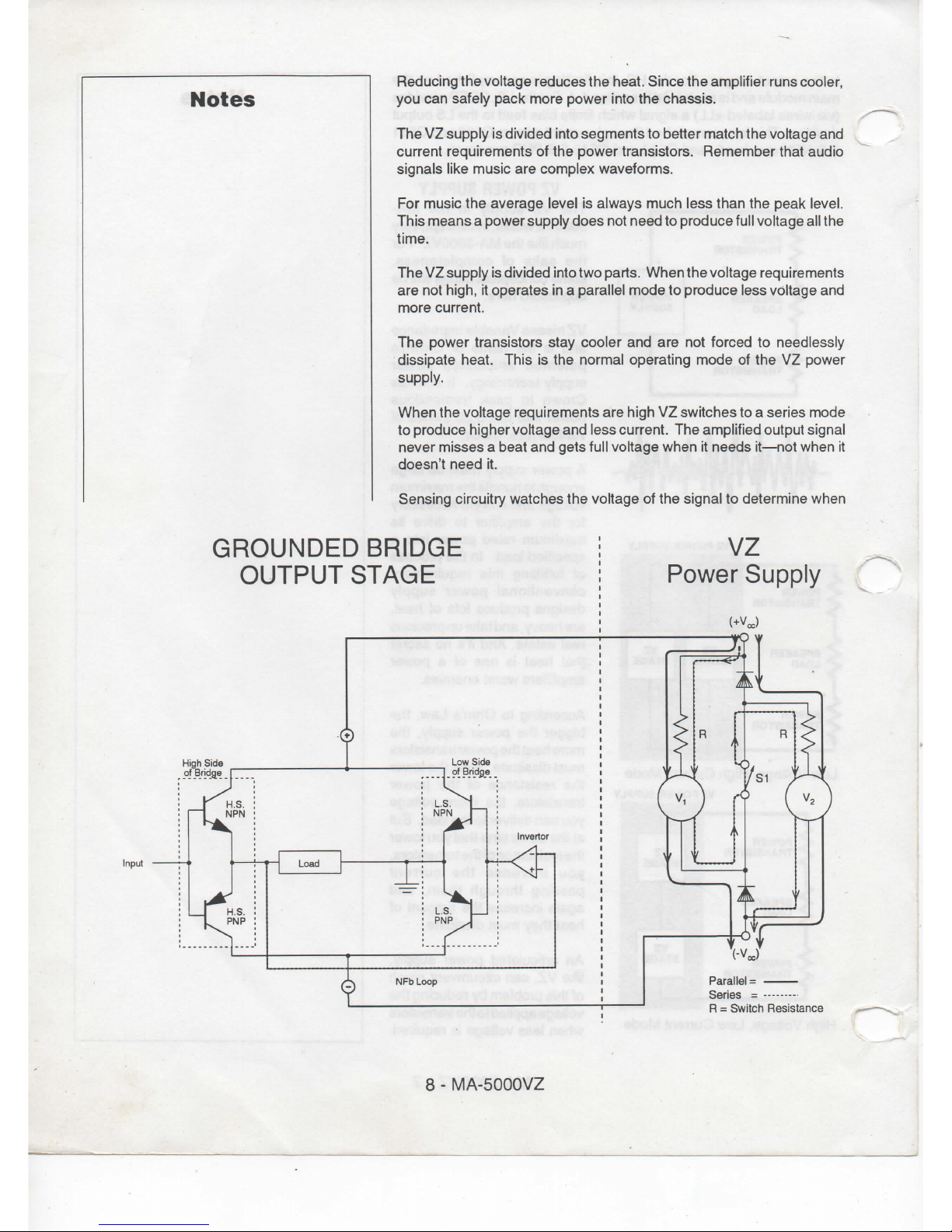
Thefour-quadrant
lopology
used
in the
grounded
oulpul
slages
is
called
Ihe
grounded bridge
and
makes
full
use of
Ihe
power supplies. This
patentad
lopology
also
makes
peak-lo-peak
voltages
available
lo
the
load which
are
twice
the
vollage
any
output
device
¡s
ever exposed
to.
The
grounded bridge
is
covered
in
detail
in the
BASICS
seclion
of
this
texl.
MA-5000VZ
- 1
Notes
The
two
channels
may be
used together
to
double
the
voltage (bridged-
mono)orthecurrent(parallel-mono)presentedto
the
load. Thisfeature
gives
the
User
flexibility
in
maximizing
the
power
available
to the
load.
Output
power
of the
amplifier
is
rated
as
follows (assumes
120V
60Hz
AC
mains):
StereoSohm:
1300W/CH
Stereo4ohm:
2000W/Ch
Stereo2ohm:
2500W/Ch
Bridge
Mono 8 ohm: 4000W
Bridge
Mono 4 ohm: 5000W
Parallel Mono 2 ohm: 4000W
Parallel Mono 1 ohm: 5000W
Macro-Tech amplifiers
utilize a wide
bandwidth
multiloop
design with
state
of the art
compensation
techniques.
This produces ideal behavior
and
results
¡n
ultra-low
distortion
valúes.
Aluminum
extrusions
have
been widely used
for
heatsinks
in
power
amplifiers
due to
their
low
cost
and
reasonable performance. However,
measured
on a
watts
per
pound
or
watts
per
volume
basis,
the
extrusión
technology
doesn't
perform
nearly
as
well
as the
thermal
diffuser
technology developed
for
Macro-Tech power amplifiers.
Our
thermal
diffusers
are
fabricated
from
custom
cut fin
stock
that
provides
an
extremely high ratio
of
área
to
volume,
or
área
to
weight.
All
power
devices
are
mounted directly
to
massive
heat
spreaders that
are
electrically hot. Making
the
heat spreaders electrically
hot
allows
MA-5000VZ:
CHANNEL1
SHOWN
4
(ooep)
MA-5000VZ Overall
Block
Diagram
D
(ODEP)
2 -
MA-5000VZ
improved thermal performance
by
eliminating
the
insulating
interface
underneath
the
power devices.
The
chassis
itself
is
used
as
part
of the
thermal circuit,
and
this
maximizes utilization
of the
available resources.
Air
flow
in
this
amplifier
is
front
to
rear,
also a departure
from
other
Macro-Techs.
Fan
speed
is a
function
of
ODEPIevel.
AlthoughODEP
was
covered
in
detail
in the
BASICS section
of
this text,
the
specif
ics of
the
MA-5000VZ ODEP circuit
are
unique
and
will
be
covered here.
Notes
OUTPUT
STAGE
CIRCUITRY
The
MA-5000VZ,
like
other Macro-Techs, uses
the
grounded bridge.
It
does
differ,
however,
in
certain
aspects.
For
example, quadrants
use
four
devices
¡n
parallel
ratherthan
the
normal máximum
of
three. Output
stages
are
also physically
built
in a
modular way,
for
ease
of
field
replacement.
Electrically, there
are
also
a few
differences.
Bias servo networks
consist
of two
transistor devices
per Vbe
multiplier (one
set for
high side,
one
set for low
side). Also, ODEP affects
the low
side
as
well
as the
high
side
by
stealing
low
side
bias
and
drive. Taking that a step further,
any
protective
action
which
limits,
mutes,
or
shuts down
the
amplifier will
accomplish
the
same thing
by
stealing drive.
Circuitry
on the
positive
and
negative output modules ¡nclude bias
circuitry,
current
limit
circuitry
(the MA-5000VZ
has two
speed current
limit),
last
voltage amplifiers (LVA's), pre-driyers, drivers,
and
output
devices. Temperature
sensors
are
also mounted
to the
heatsinks
vía
the
output modules. These deliver ¡nformation
to the
main
module
which
computes actual calibrated temperature
for
ODEP
and
temperature
measurement.
H-15V
R571
2.7K
Positive
(NPN) Output
Stage
Thermal
Sensor Circuitry
U50O
V.
LM334
r
L
3
R572
r£
227
O.5OW
R584
2.7K
\
+TEMP1
:
The
positive
LVA's
(Q501,
Q502,
and
Q503)convert
the
negative
output
of
the
voltage translator stage
to a
positive drive voltage
for the NPN
High
Side
(HS) predriver. There
are
three
LVAtransistorsin
parallel
due
to
the
very
high
voltages
(therefor
higher
current
and
thermal
requirements) that
are
present
when
the
power
supply
is in
high voltage
mode.
D522
prevenís
the
+LVA'sfromproducinga
high negative output
to the HS NPN
stage.
MA-5000VZ
- 3
Notes
Q507, Q508,
and
Q509
are the
-LVA's
and are
arranged
¡n
mirror
image
to
the
+LVA's,
¡ncluding
D513.
On
the
positive side D514, D515,
and
C506
vía
the
+LVA's
act to
limit
slew
rate.
D514
and
D515
also
prevent dangerously excessive current
through
the
LVA's.
D516,
D517,
and
C507
are the
negative
HS
mirror
image.
Q534
and
Q540
provide
two-speed current limiting
¡n the
output stage.
Sense
lines
are
arranged such that excessive current through
any
single
HS
output device
will
result
in
current limit protection. Q535
and
Q541
are
the
negative side mirror image.
Q503
on the
positive output module works
in
tándem with Q505
on the
negative output module
as a Vbe
multiplier
circuit.
They produce and,
with great
stabilily,
control
biasforthe
High Side
NPN
and
PNP
devices.
Potentiometer R505
is
used precisely
set
bias voltage. Bias voltage
is
easily measured
from
pin 2
(hot)
to pin 4 of ATE
ports
TP1 and
TP2.
Refer
to
section
2 for
appropriate test procedures.
Q504¡stheHSNPNpre-driverandQ511
istheHSNPNdriver.
These
devices
are
biased
class
AB for
ultra
low
distortion
in the
zero-crossing
región.
Q513, Q515,
Q517,
and
Q536
are the HS NPN
output devices. These
devices
are
biased
class
B, in
soft
cut-off,
Together
with
driver
and
pre-
driver, they function
as a
three-deep Darlington.
The
output devices
work
¡n
parallel
as a
giant composite.
The
over-all
bias topology
is
referred
to as
AB+B,
originally conceived
and
patented
by
Crown
engineers
in
1966.
This
¡s
still
the
most
efficient,
stable,
and
distortion
free
method used today.
Positive
LVA,
Portion
of HS
Bias,
&
Positive
Current
Limit
Section
VCC1
High Side
+LVA's,
Current
Limit,
and the
portion
of the
Bias
Servo
Network
on the
Positive Output
Module.
D51O
R595
3
82K
C536
O.O01
r-
R5O5
HIGH)
500
SIDE
';
BIAS
U
Emitter
Sense
Output
Audio
4 -
MA-5000VZ
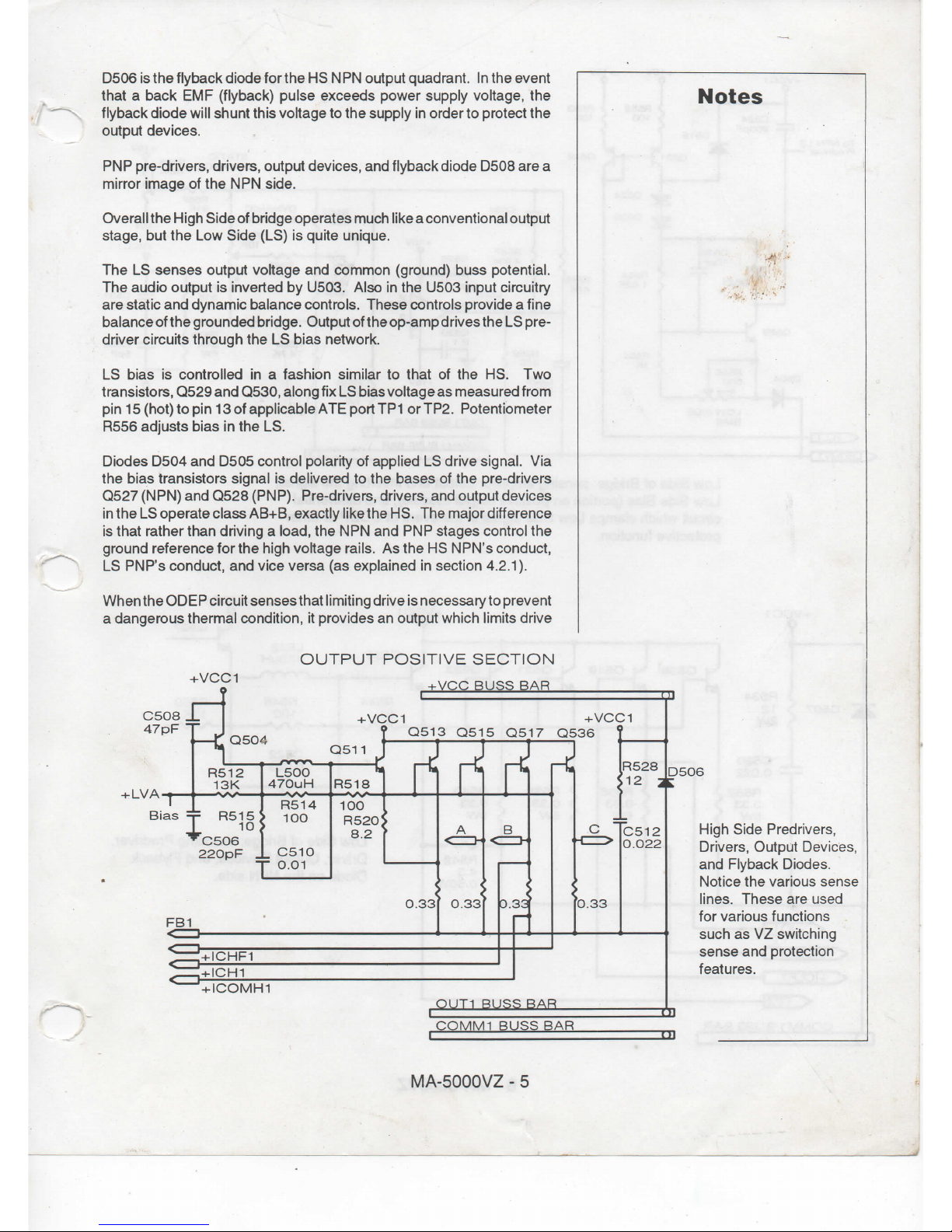
D506
is
theflybackdiode
forthe
HS NPN
output quadrant.
In
the
event
that a back
EMF
(flyback) pulse exceeds power supply voltage,
the
flyback
diode
will
shunt this voltage
to the
supply
in
order
to
protect
the
output devices.
PNP
pre-drivers,
drivers,
output devices,
and
flyback diode D508
are a
mirror
image
of the NPN
side.
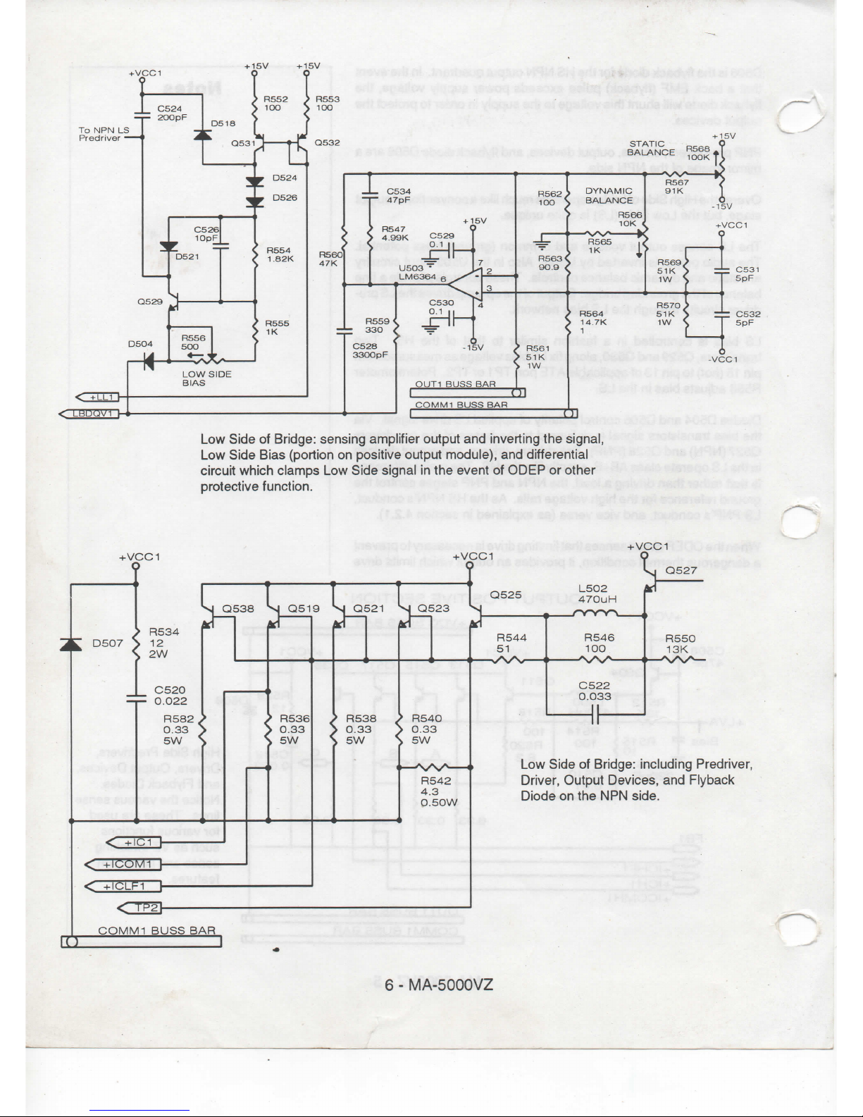
Overall
the
High
Side
of
bridge operates much
like a conventional output
stage,
but the Low
Side
(LS)
is
quite unique.
The LS
senses output voltage
and
common
(ground) buss potential.
The
audio output
is
inverted
by
U503.
Also
in the
U503 input
circuitry
are
static
and
dynamic balance controls.
These
controls provide a fine
balance
of the
grounded bridge. Output
of the
op-amp
drives
the LS
pre-
driver
circuits
through
the LS
bias network.
LS
bias
¡s
controlled
in a
fashion
similar
to
that
of the HS. Two
transistors, Q529
and
Q530,
along
fix LS
bias voltage
as
measured
from
pin
15(hot)topin13ofapplicableATEportTP1
orTP2. Potentiometer
R556
adjusts
bias
in the LS.
Diodes D504
and
D505 control
polarity
of
applied
LS
drive signal.
Via
the
bias transistors signal
¡s
delivered
to the
bases
of the
pre-drivers
Q527
(NPN)
and
Q528 (PNP).
Pre-drivers,
drivers,
and
output devices
in
the LS
opérate
class
AB+B,
exactly
like
the HS. The
major
difference
¡s
that
rather
than driving a load,
the NPN and PNP
stages control
the
ground reference
for the
high
voltage
rails.
As the HS
NPN's conduct,
LS
PNP's conduct,
and
vice versa
(as
explained
in
section
4.2.1).
When
the
ODEP circuit senses that limiting drive
is
necessary
to
prevent
a
dangerous thermal
condition,
¡t
provides
an
output which limits drive
Notes
+VCC1
OUTPUT POSITIVE SECTION
+VCC
BUSS
BAR
+
LVA
H-VCC1
Q513
Q515 Q517
Q536
'
C5O6
220pF
_L
C510
'
O.O1
D5O6
High Side Predrivers,
Drivers,
Output
Devices,
and
Flyback Diodes.
Notice
the
various sense
lines.
These
are
used
for
various functions
such
as VZ
switching
sense and
protection
features.
MA-5000VZ
- 5
-I-VCC1
o
I-15V
I-15V
C524
2OOpF
R552
1OO
R553
1OO
To
NPN LS
Predriver
D518
D5
J
D4
y
H
I
C52
10p
D521
N
d
RS56
500
4
1
LOW S
BIAS
6
=
f
>>[
5
5
— <
DE
A
^
D5£
r
os:
R554
1
.821
'
R555
>
1K
k
4
6
<
l
R56O
47K
_L
C534
!47pF
R547
4.99K
C52S
xH
U5O3
•
LM6364
g
JjH
—
C528
33OOpF
OUT1
B
I
COMM1
1
'
1
15V
Low
Side
of
Bridge: sensing amplifier output
and
¡nverting
the
signal,
Low
Side Bias
(portion
on
positive output module),
and
differential
circuit which clamps
Low
Side signal
¡n the
event
of
ODER
or
other
protective function.
+VCC1
+VCC1
+VCC1
Q527
I
L
tí
>
H534
¡T
D507 > 12
X
2W
C520
r-
0.022
R582
¿
0.
33
>
5W
S
Q538
V|
Q51
r
¿
R536
>
0.33
S 5W
•
i
BU
rj
S
R538
/
>
0.33
>
S
5W
S
i
Q523
R54O
0.33
5W
-*S
V"
R542
4.
0.350W
rNr^^>1^J
l-t
Ql
ice; n A
c
(
Q525
470uH
N
-
r^^V^VN
.
*T
R544
R546
51
100
C522
0.033
||
kr
R550
13K
ni
Low
Side
of
Bridge: including
P
Driver, Output Devices,
and
Fl^
Diode
on the NPN
side.
LLL
6 -
MA-5000VZ
to
the
output
stages.
For the HS,
this
limiting
¡s
accomplished
on the
main module
and
isexplained
¡nsect¡on4.4.
Forthe
LS,
ODEP provides
(via wires
labeled
±LL) a signal
which
limits bias feed
to the LS
output
devices. This
is
accomplished through current mirrors Q532
and
Q531
(LS
NPN
quadrant),
and
Q542
and
Q543
(LS PNP
quadrant).
Notes
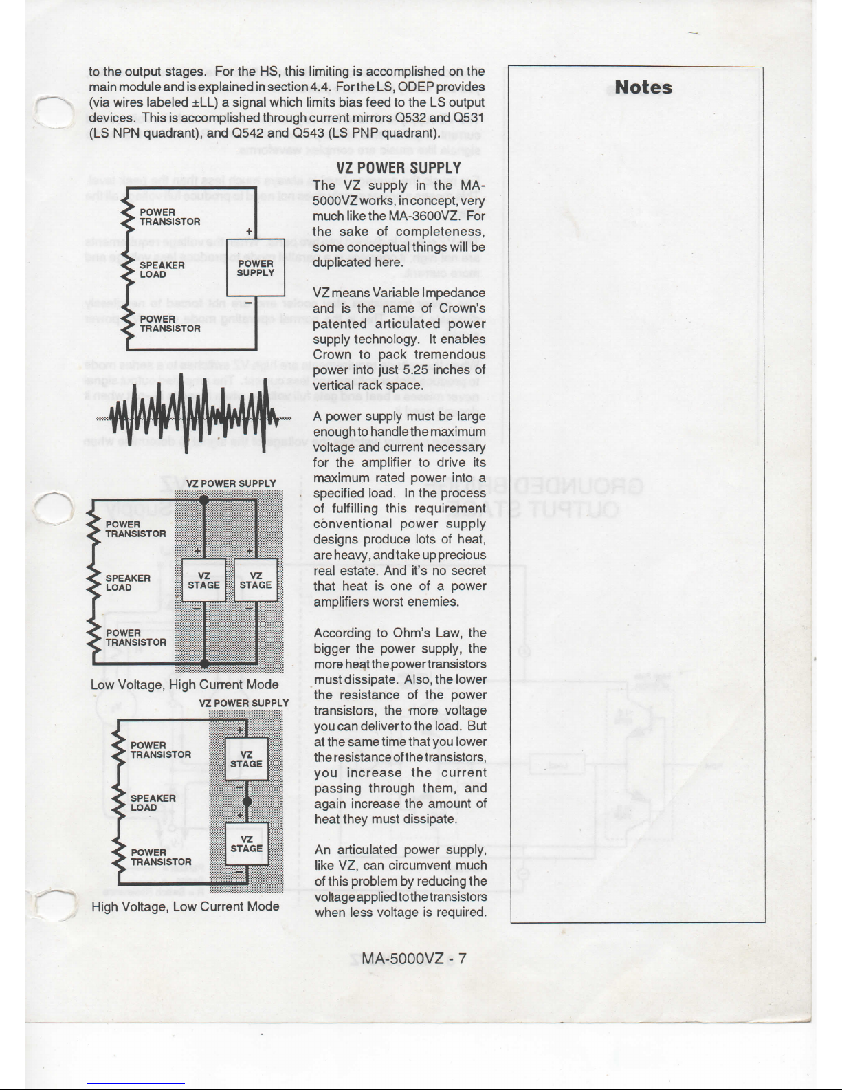
POWER
TRANSISTOR
SPEAKER
LOAD
POWER
TRANSISTOR
VZ
POWER
SUPPLY
POWER
TRANSISTOR
SPEAKER
LOAD
POWER
TRANSISTOR
VZ
STAGEVZSTAGE
Low
Voltage, High Current Mode
VZ
POWER SUPPLY
POWER
TRANSISTOR
SPEAKER
LOAD
POWER
TRANSISTOR
VZ
STAGE
VZ
STAGE
High Voltage,
Low
Current Mode
VZ
POWER
SUPPLY
The VZ supply in the MASOOOVZworks,
inconcept,
very
much
like
the
MA-3600VZ.
For
the
sake
of
completeness,
some
conceptual things
will
be
duplicated
here.
VZ
means
Variable Impedance
and is the
ñame
of
Crown's
patented
articulated
power
supply technology.
It
enables
Crown
to
pack tremendous
power
into just 5.25 inches
of
vertical
rack
space.
A
power supply must
be
large
enough
to
handle
the
máximum
voltage
and
current
necessary
for
the
amplifier
to
drive
its
máximum rated power into
a
specified load.
In the
process
of
fulfilling this requirement
cónventional power supply
designs produce
lots
of
heat,
are
heavy,
and
take
up
precious
real
estáte.
And
it's
no
secret
that heat
is one of a
power
amplifiers worst enemies.
According
to
Ohm's Law,
the
bigger
the
power supply,
the
more
heai
the
power
transistors
must
dissipate.
Also,
the
lower
the
resistance
of the
power
transistors,
the
more voltage
you
can
deliverto
the
load.
But
at
the
same time that
you
lower
the
resistance
of
the
transistors,
you
increase
the
current
passing through
them,
and
again ¡ncrease
the
amount
of
heat
they must dissipate.
An
articulated power
supply,
like
VZ, can
circumvent much
of
this problem
by
reducing
the
voltage
appliedto
the
transistors
when
less
voltage
is
required.
MA-5000VZ
- 7
Notes
Reducing
the
voltage
reduces
the
heat.
Since
the
amplifier
runs
cooler,
you can
safely pack more power into
the
chassis.
The VZ
supply
is
divided ¡nto segments
to
better match
the
voltage
and
current
requirements
of the
power transistors. Remember that audio
signáis
like
music
are
complex waveforms.
For
music
the
average
level
is
always
much
less
than
the
peak
level.
This
means a power supply does
not
need
to
produce full voltage
all
the
time.
The
VZ
supply
is
divided
into
two
parís.
When
the
voltage requirements
are
not
high,
it
opérales
in a
parallel mode
to
produce less vollage
and
more current.
The
power transistors
slay
cooler
and are
nol
torced
lo
needlessly
dissipate
heal.
This
is
Ihe
normal
operaling
mode
of
Ihe
VZ
power
supply.
When
Ihe
vollage
requiremenls
are
high
VZ
swilches
to a
series mode
to
produce higher
vollage
and
less
currenl.
The
amplified
oulpul
signal
never
misses a beal
and
gels
full vollage when
it
needs
il—not
when
il
doesn't need
¡t.
Sensing
circuilry
walches
Ihe
vollage
of
Ihe
signal
lo
delermine when
GROUNDEDBRIDGE
OUTPUT STAGE
Input
VZ
Power
Supply
^
R = Switch
Resistance
8 -
MA-5000VZ
to
switch
VZ
modes.
The
switching
circuitry
is
designed
to
prevent
audible
switching
distortion
to
yield
the
highest dynamic transfer
function—you
hear
only
the
musió
and not the
amplifier.
You get not
only
the
máximum power with
the
máximum safety,
you
also
get
the
best
power
matching
to
your load.
Actual
current
flow
with power supply
and
grounded bridge operating
together
is
shown
on the
previous page.
The
individual
components
are
shown
below.
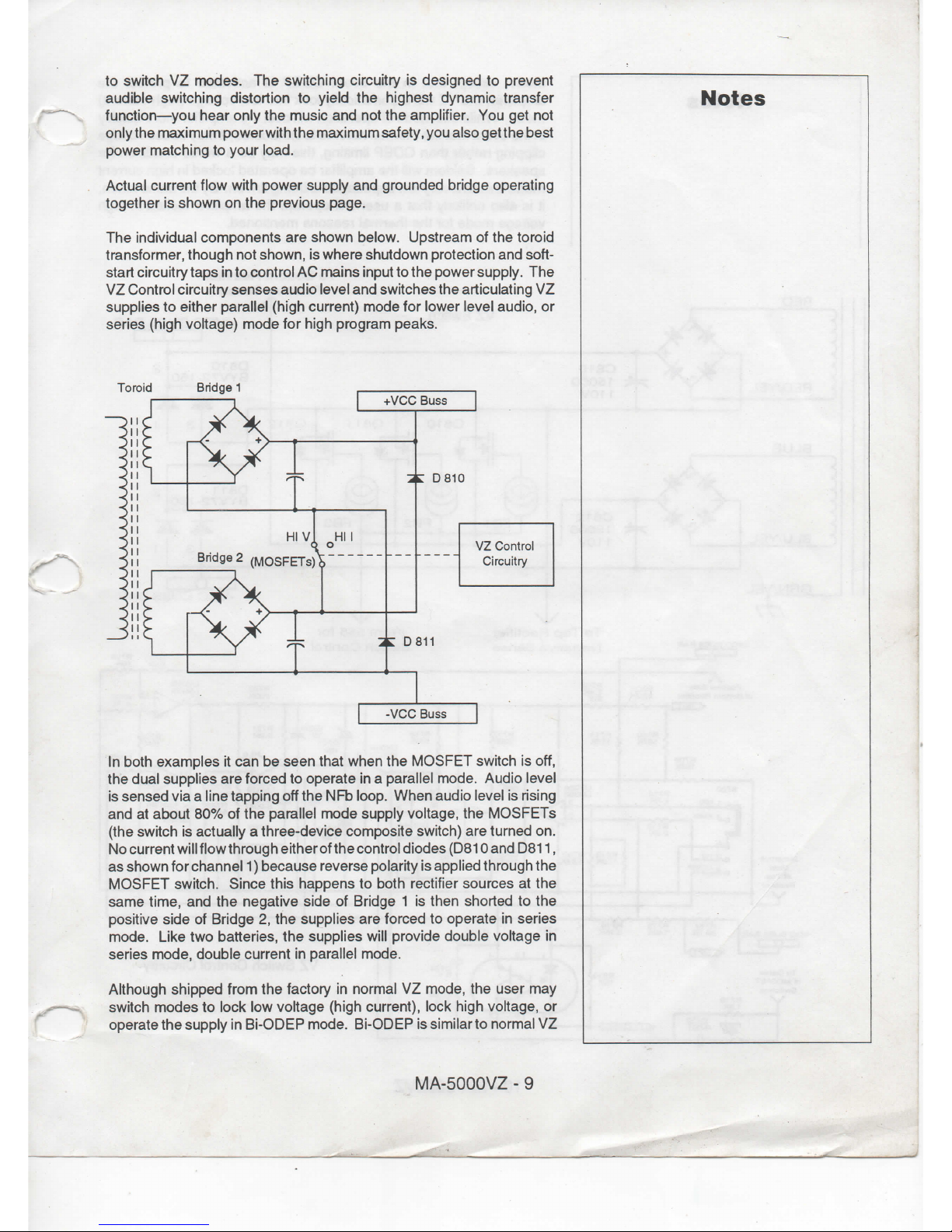
Upstream
of the
toroid
transformer,
though
not
shown,
is
where shutdown protection
and
soft-
start
circuitry taps
in to
control
AC
mains ¡nput
to the
power
supply.
The
VZ
Control circuitry senses
audio
level
and
switches
the
articulating
VZ
supplies
to
either parallel (high current) mode
for
lower
level audio,
or
series
(high voltage) mode
for
high program peaks.
Notes
Toroid
Bridge
1
In
both examples
it can be
seen that
when
the
MOSFET switch
is
off,
the
dual
supplies
are
torced
to
opérate
¡n a
parallel mode. Audio level
is
sensed
via a
line
tapping
off the
NFb
loop.
When audio level
¡s
rising
and at
about
80% of the
parallel
mode supply voltage,
the
MOSFETs
(the
switch
is
actually a three-device
composite switch)
are
turned
on.
No
current
will
flow through either
of the
control diodes
(D810
and
D811,
as
shown
for
channel
1)
because reverse polarity
is
applied through
the
MOSFET switch. Since
this
happens
to
both rectifier sources
at the
same time,
and the
negative side
of
Bridge
1 ¡s
then
shorted
to the
positive side
of
Bridge
2, the
supplies
are
forced
to
opérate
in
series
mode.
Like
two
batteries,
the
supplies will provide double voltage
in
series mode, double current
¡n
parallel mode.
Although
shipped
from
the
factory
¡n
normal
VZ
mode,
the
user
may
switch
modes
to
lock
low
voltage (high current),
lock
high voltage,
or
opérate
the
supply
in
Bi-ODEP mode. Bi-ODEP
is
similar
to
normal
VZ
MA-5000VZ
- 9
 Loading...