

Page 1
Page 2

Revision Control
Revision Print Date
Initial Release (K80713–9) June 1996
Revision 1 (101033–1) November 1996
Revision 2 (101033–2) August 1997
Revision 3 (900239–1) February 1998
Revision 4 (900239–1) October 1998
Revision 5 (901047-1) October 1999
Revision 6 (901047-2) May 2000
Revision 7 March 2002
Revision 8 February 2006
Important Notices
©2006, Crown Broadcast, a division of International Radio and Electronics, Inc.
Portions of this document were originally copyrighted by Michael P. Axman in 1991.
All rights reserved. No part of this publication may be reproduced, transmitted,
transcribed, stored in a retrieval system, or translated into any language in any
form by any means without the written permission of Crown International, Inc.
Printed in U.S.A.
Sony and RCA are trademarks of their respective companies.
Crown attempts to provide information that is accurate, complete, and useful.
Should you find inadequacies in the text, please send your comments to the following address:
International Radio and Electronics
25166 Leer Drive, P.O . Box 2000
Elkhart, Indiana, 46515-2000 U .S.A.
ii
Page 3

ContentsContents
Contents
ContentsContents
Section 1—Getting Acquainted ..................................... 1–1
1.1 Your Transmitter ...............................................................................................1–2
1.2 Applications and Options...................................................................................1–3
1.2.1 Stand-Alone ..................................................................................................1–4
1.2.2 Backup..........................................................................................................1–4
1.2.3 Booster .........................................................................................................1–4
1.2.4 Exciter...........................................................................................................1–4
1.2.5 T ranslator......................................................................................................1–5
1.2.6 Satellator ......................................................................................................1–6
1.3 T ransmitter/Exciter Specifications .....................................................................1–7
1.4 Receiver Specifications .....................................................................................1–9
1.5 Safety Considerations......................................................................................1–10
1.5.1 Dangers ......................................................................................................1–10
1.5.2 Warn ings ....................................................................................................1–10
1.5.3 Cautions......................................................................................................1–10
Section 2—Installation ............................................... 2–1
2.1 Operating Environment......................................................................................2–2
2.2 Remove PA Tray Spacers ..................................................................................2–2
2.3 Power Connections ...........................................................................................2–3
2.4 Frequency (Channel) Selection ..........................................................................2–5
2.4.1 Modulation Compensator..............................................................................2–6
2.4.2 RF T uning Adjustments.................................................................................2–7
2.5 Receiver Frequency Selection............................................................................2–7
2.6 RF Connections.................................................................................................2–9
2.7 Audio Input Connections .................................................................................2–10
2.8 SCA Input Connections ...................................................................................2–11
2.9 Composite Input Connection ........................................................................... 2–11
2.10 Audio Monitor Connections.............................................................................2–12
2.11 Pre-emphasis Selection...................................................................................2–12
2.12 Processor Bypass Option ................................................................................2–12
2.13 Program Input Fault Time-out .........................................................................2–13
2.14 Remote I/O Connector.....................................................................................2–13
iii
Page 4

Section 3—Operation................................................. 3–1
3.1 Initial Power-up Procedures ..............................................................................3–2
3.2 Power Switches.................................................................................................3–4
3.2.1 DC Breaker....................................................................................................3–4
3.2.2 Power Switch................................................................................................3–4
3.2.3 Carrier Switch...............................................................................................3–4
3.3 Front Panel Bar-Dot Displays.............................................................................3–5
3.3.1 Audio Processor Input ..................................................................................3–5
3.3.2 Highband and Wideband Display ..................................................................3–5
3.3.3 Modulation Display .......................................................................................3–5
3.5 Processing Control............................................................................................3–6
3.6 Stereo-Mono Switch..........................................................................................3–6
3.4 Input Gain Switches ..........................................................................................3–6
3.7 RF Output Control .............................................................................................3–7
3.8 Digital Multimeter..............................................................................................3–7
3.9 Fault Indicators .................................................................................................3–8
Section 4—Principles of Operation................................. 4–1
4.1 Part Numbering.................................................................................................4–2
4.2 Audio Processor Circuit Board ..........................................................................4–3
4.3 Stereo Generator Circuit Board..........................................................................4–4
4.4 RF Exciter Circuit Board ....................................................................................4–6
4.5 Metering Circuit Board ......................................................................................4–8
4.6 Motherboard .....................................................................................................4–9
4.7 Display Circuit Board.......................................................................................4–10
4.8 Voltage Regulator Circuit Board ......................................................................4–11
4.9 Power Regulator Circuit Boards ......................................................................4–12
4.10 RF Driver.........................................................................................................4–12
4.11 RF Amplifier ....................................................................................................4–13
4.12 Chassis ...........................................................................................................4–13
4.13 RF Output Filter & Reflectometer.....................................................................4–14
4.15 Receiver Circuit Board Option .........................................................................4–14
iv
Page 5

Section 5—Adjustments and Tests ................................. 5–1
5.1 Audio Processor Adjustments ...........................................................................5–2
5.1.1 Pre-Emphasis Selection ................................................................................5–2
5.1.2 Pre-Emphasis Fine Adjustment .....................................................................5–2
5.2 Stereo Generator Adjustments ..........................................................................5–3
5.2.1 Separation ....................................................................................................5–3
5.2.2 Composite Output.........................................................................................5–3
5.2.3 19 kHz Level .................................................................................................5–3
5.2.4 19 kHz Phase................................................................................................5–3
5.3 Frequency Synthesizer Adjustments ..................................................................5–4
5.3.1 Frequency (Channel) Selection......................................................................5–4
5.3.2 Modulation Compensator..............................................................................5–4
5.3.3 Frequency Measurement and Adjustment .....................................................5–4
5.3.4 FSK Balance Control .....................................................................................5–4
5.4 Metering Board Adjustments.............................................................................5–5
5.4.1 Power Calibrate.............................................................................................5–5
5.4.2 Power Set .....................................................................................................5–5
5.4.3 SWR Calibrate...............................................................................................5–5
5.4.4 P A Current Limit ...........................................................................................5–5
5.5 Motherboard Adjustments.................................................................................5–6
5.6 Display Modulation Calibration..........................................................................5–6
5.7 Voltage Regulator Adjustments .........................................................................5–6
5.8 Bias Set (RF Power Amplifier)...........................................................................5–6
5.9 Performance Verification ...................................................................................5–7
5.9.1 Audio Proof-of-Performance Measurements .................................................5–7
5.9.2 De-emphasis Input Network..........................................................................5–7
5.10 Carrier Frequency..............................................................................................5–8
5.11 Output Power ....................................................................................................5–8
5.12 RF Bandwidth and RF Harmonics......................................................................5–8
5.13 Pilot Frequency .................................................................................................5–8
5.14 Audio Frequency Response ...............................................................................5–9
5.15 Audio Distortion ................................................................................................5–9
5.16 Modulation Percentage......................................................................................5–9
5.17 FM and AM Noise..............................................................................................5–9
5.18 Stereo Separation..............................................................................................5–9
5.19 Crosstalk ...........................................................................................................5–9
5.19.1 Main Channel Into Sub ..............................................................................5–10
5.19.2 Sub Channel Into Main ..............................................................................5–10
5.20 38 kHz Subcarrier Suppression.......................................................................5–10
5.21 Additional Checks............................................................................................5–10
v
Page 6

Section 6—Reference Drawings .................................... 6–1
6.1 Views ................................................................................................................6–2
6.2 Board Layouts and Schematics .........................................................................6–4
Section 7—Service and Support.................................... 7 –1
7.1 Service ..............................................................................................................7–2
7.2 24–Hour Support ..............................................................................................7–2
7.3 Spare Parts .......................................................................................................7–2
Appendix................................................................ A–1
Glossary.................................................................G–1
Index................................................................Index–1
Page 7
I
INFORMATION
Section 1—Getting Acquainted
This section provides a general description of the FM500 transmitter and introduces you to safety conventions used within this
document. Review this material before installing or operating
the transmitter.
Getting Acquainted
1–1
Page 8
I
1.1 Your Transmitter
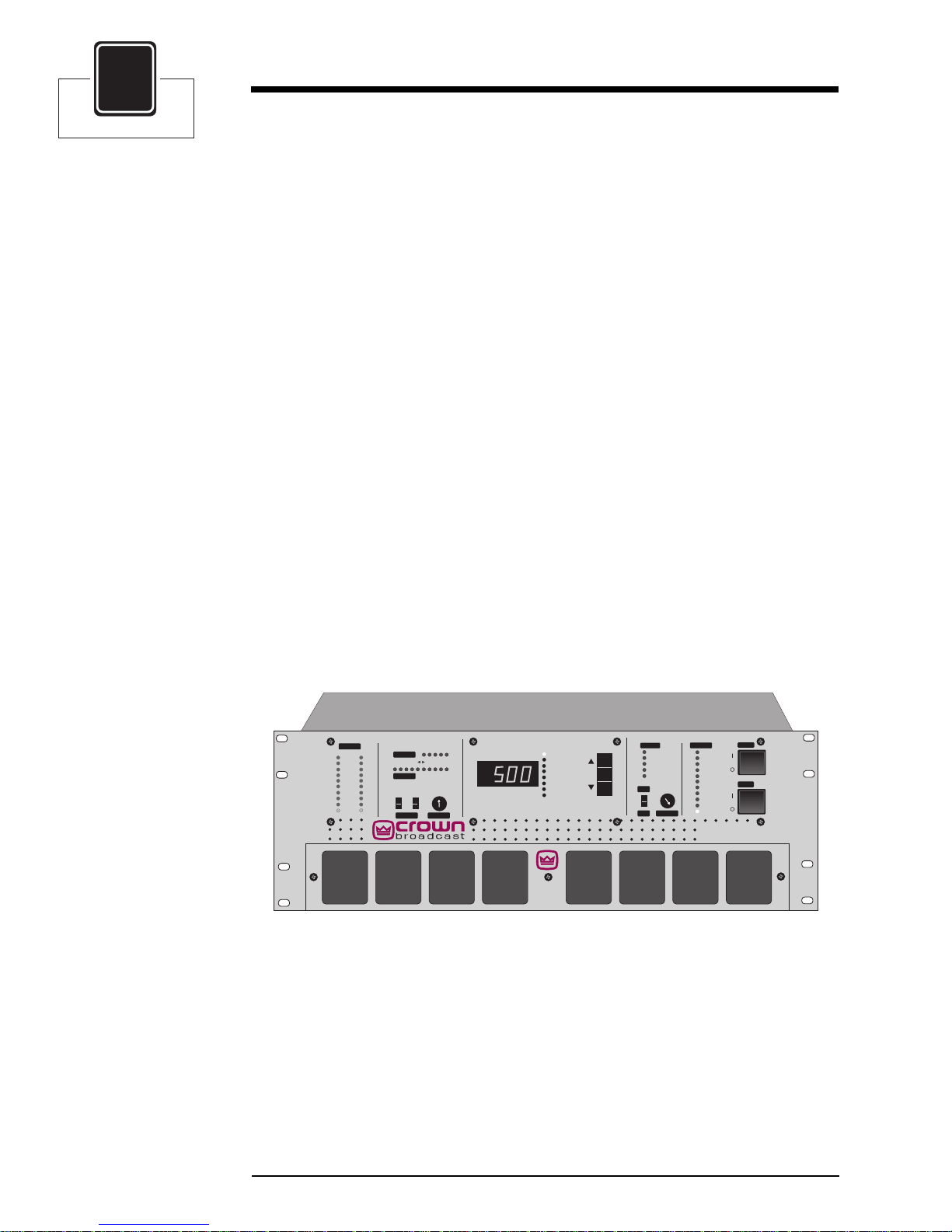
The FM500 is a member of a family of FM stereo broadcast transmitters. Crown
transmitters are known for their modularity, ease-of-use, and reliability.
The modularity is most apparent in the standard transmitter configuration which
incorporates audio processing, stereo generation, and RF amplification without
compromised signal quality. A single Crown transmitter can replace several pieces
of equipment in a traditional system.
Ease-of-use is apparent in the user-friendly front panel interface and in the installation procedure. Simply select your operating frequency (using four rotary
switches), add an audio source, attach an antenna, connect AC power, and you're
ready to broadcast. Of course, the FM series of transmitters also feature more
sophisticated inputs and monitoring connections if needed.
Reliability is a Crown tradition. The first Crown transmitters were designed for
rigors of worldwide and potentially portable use. The modular design, quality
components, engineering approach, and high production standards ensure stable
performance.
Remote control and metering of the transmitter is made possible through a builtin I/O port. For more direct monitoring, the front panel includes a digital multimeter display and status indicators. Automatic control circuitry provides protection for high VSWR as well as high current, voltage, and temperature conditions.
Audio Input
High
-12
-18
Low
Modulation
10
2
High Band
Expand
Compress
2
-6
Wide Band
+6 dB
20
+12 dB
ProcessingInput Gain
®
RF Power
SWR
ALC
PA DC Volts
PA DC Amps
PA Temperature
Supply DC Volts
Voltmeter
Fault
SWR
Lock
Input
PA DC
PA Temp
Stereo
Mono RF Output
Carrier
Over
100
90
80
70
60
Power
50
40
30
20
Pilot
FM500
FM BROADCAST TRANSMITTER
Illustration 1–1 FM500 Stereo Broadcast Transmitter
1–2
FM500 User's Manual
Page 9
1.2 Applications and Options
Crown transmitters are designed for versatility in applications. They have been used
as stand-alone and backup transmitters and in booster, translator, and satellator
applications. The following discussion describes these applications further.
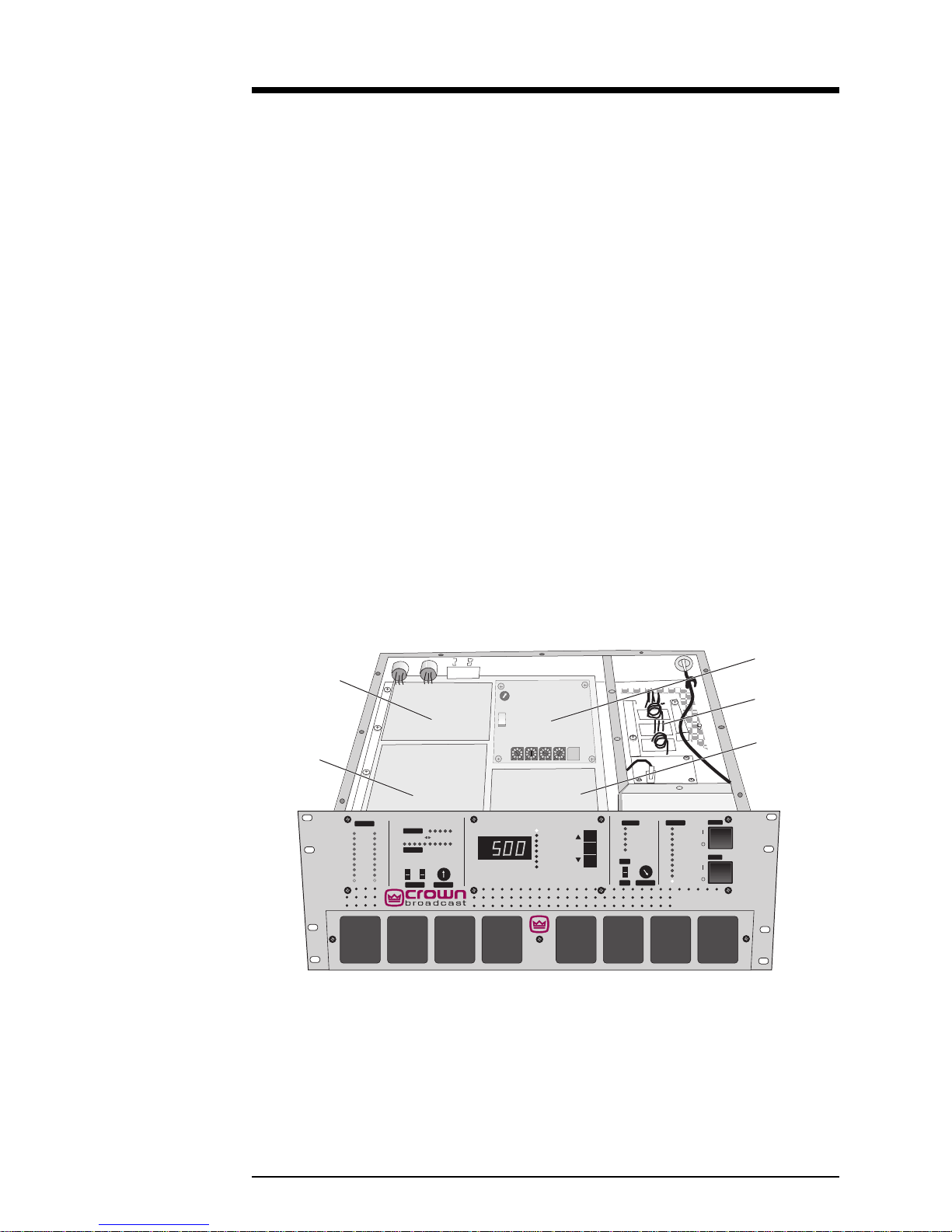
Model numbers describe the configuration of the product (which has to do with its
intended purpose) and the RF output power which you can expect.
The number portion of each name represents the maximum RF output power. The
FM500, for example, can generate up to 500 watts of RF output power.
Suffix letters describe the configuration. The FM500T, for example, designates a
"transmitter" configuration. Since this is standard, it is what is described in the
manual except where specified. In this configuration, the product includes the
following modules (functions):
❑ audio processor
❑ stereo generator
❑ RF exciter
❑ metering
❑ low-pass filter
Stereo Generator
Audio Processor
Audio Input
10
High
-6
-12
-18
Low
2
Wide Band
+6 dB
Expand
Compress
20
+12 dB
ProcessingInput Gain
®
2
High Band
RF Power
SWR
ALC
PA DC Volts
PA DC Amps
PA Temperature
Supply DC Volts
Voltmeter
Fault
SWR
Lock
Input
PA DC
PA Temp
Stereo
Mono RF Output
Over
100
90
80
70
60
Power
50
40
30
20
Pilot
FM500
FM BROADCAST TRANSMITTER
Carrier
Modulation
Illustration 1–2 Standard (Transmitter) Configuration
RF Exciter
Low-pass Filter
Metering
Getting Acquainted
1–3
Page 10

I
1.2.1 Stand-Alone
In the standard configuration, the FM500 is an ideal stand-alone transmitter.
When you add an audio source (monaural, L/R stereo, or composite signal), an
antenna, and AC power, the transmitter becomes a complete FM stereo broadcast
station, capable of serving a community.
As stand-alone transmitters, Crown units often replace multiple pieces of equipment in a traditional setup (exciter, audio processor, RF amplifier).
1.2.2 Backup
In the standard configuration, Crown transmitters are also used in backup applications. Should your primary transmitter become disabled, you can continue to
broadcast while repairs take place. In addition, the FM transmitters can replace
disabled portions of your existing system including the exciter, audio processor, or
amplifier. Transfer switches on each side of the existing and backup transmitters
make the change-over possible with minimal downtime.
1.2.3 Booster
Also in the standard configuration, Crown transmitters have been used as booster
transmitters. Booster applications typically involve certain geographic factors
which prevent your system from broadcasting to the full coverage area allowable.
For example, a mountain range might block your signal to a portion of your
coverage area. Careful placement of a Crown transmitter, operating on the same
frequency as your primary transmitter, can help you reach full coverage.
1.2.4 Exciter
In addition to the standard configuration, the FM500 is available in optional
configurations to meet a variety of needs.
An "E" suffix, as in the FM500E, for example, represents an exciter-only configuration. In this configuration, the audio processor and stereo generator are not
included. The exciter configurations are the least expensive way to get Crownquality components into your transmission system.
You might consider the Crown exciter when other portions of your system are
performing satisfactorily and you want to maximize your investment in present
equipment.
1–4
FM500 User's Manual
Page 11
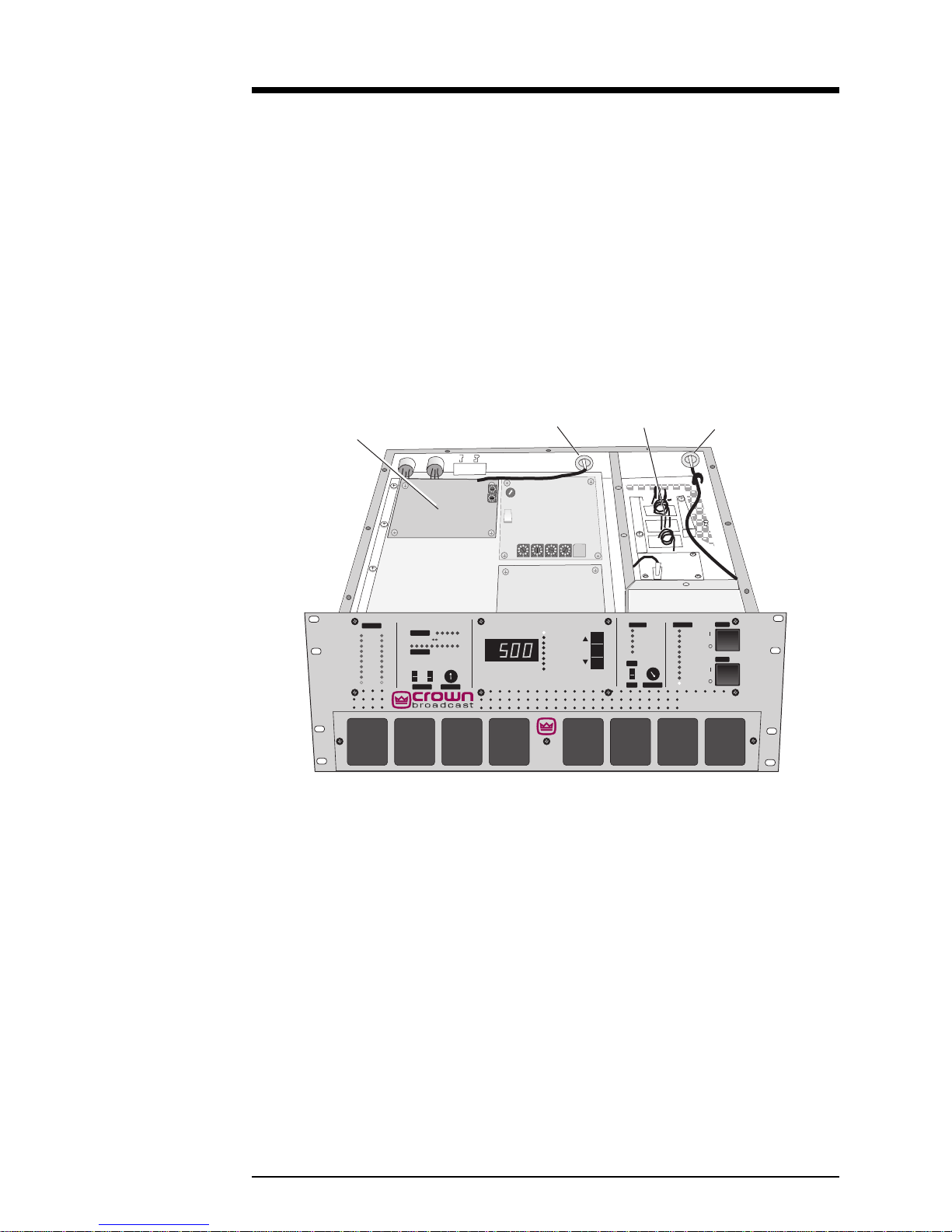
1.2.5 Translator
A receiver configuration (FM500R, for example) takes an exciter configuration and
adds receiver circuitry as well. This added feature makes the FM500 ideal for
translator service in terrestrial-fed networks. These networks represent a popular
and effective way to increase your broadcasting coverage. Translators, acting as
repeater emitters, are necessary links in this chain of events.
Traditionally, network engineers have relied on multiple steps and multiple pieces
of equipment to accomplish the task. Others have integrated the translator
function (receiver and exciter) to feed an amplifier. Crown, on the other hand,
starts with an integrated transmitter and adds a solid-state Receiver Module to
form the ideal translator.
Receiver Module
RF IN
Low-pass Filter
RF Out
(option)
Stereo
Generator
RF Exciter
Metering
Audio Input
10
High
-6
-12
-18
Low
Expand
Compress
2
20
Wide Band
+12 dB
+6 dB
ProcessingInput Gain
®
2
High Band
RF Power
SWR
ALC
PA DC Volts
PA DC Amps
PA Temperature
Supply DC Volts
Voltmeter
Fault
SWR
Lock
Input
PA DC
PA Temp
Stereo
Mono RF Output
Over
100
90
80
70
60
Power
50
40
30
20
Pilot
FM500
FM BROADCAST TRANSMITTER
Carrier
Modulation
Illustration 1–3 Crown's Integrated Translator
This option enables RF in and RF out on any of Crown’s FM series of transmitters.
In addition, the module supplies a composite output to the RF exciter portion of
the transmitter. From here, the signal is brought to full power by the built-in
power amplifier for retransmission. The Receiver Module has been specifically
designed to handle SCA channel output up to 100 kHz for audio and high-speed
data.
FSK ID programming is built-in to ensure compliance with FCC regulations
regarding the on-air identification of translators. Simply specify the call sign of
the repeater station when ordering. Should you need to change the location of the
translator, replacement FSK chips are available. The Receiver Module option
should be ordered at the time of initial transmitter purchase. However, an option
kit is available for field converting existing Crown units.
Getting Acquainted
1–5
Page 12
I
1.2.6 Satellator
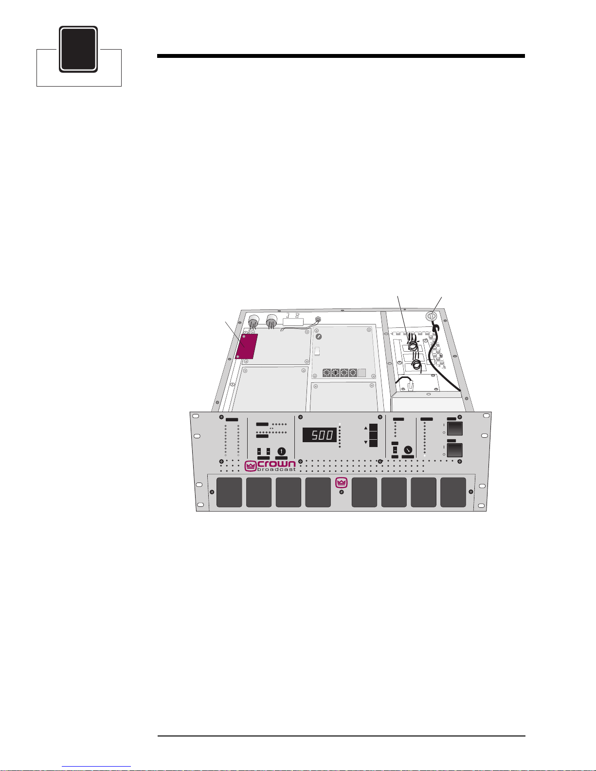
Another option is available for all configurations—an FSK Identifier (FSK IDer).
This added feature enables the FM500 to transmit its call sign or operating frequency in Morse Code. This option is intended for use in satellite-fed networks.
Transmitters equipped in this fashion are often known as "satellators."
Connect the transmitter to your satellite receiver and the pre-programmed FSK
IDer does the rest—shifting the frequency to comply with FCC requirements and
in a manner that is unnoticeable to the listener. The FSK IDer module should be
ordered at the time you order your transmitter but is available separately (factory
programmed for your installation).
Add the FSK IDer option to the exciter configuration for the most economical
satellator (a composite input signal is required).
FSK IDer
(option)
Low-pass Filter
Stereo
Generator
RF Exciter
Audio
Audio Input
High
-6
-12
-18
Low
Processor
2
High Band
Expand
Compress
2
Wide Band
+12 dB
+6 dB
ProcessingInput Gain
10
20
®
Metering
RF Power
SWR
ALC
PA DC Volts
PA DC Amps
PA Temperature
Supply DC Volts
Voltmeter
Fault
SWR
Lock
Input
PA DC
PA Temp
Stereo
Mono RF Output
Modulation
Over
100
90
80
70
60
50
40
30
20
Pilot
FM500
FM BROADCAST TRANSMITTER
Illustration 1–4 Transmitter with FSK IDer Option
RF Out
Carrier
Power
1–6
FM500 User's Manual
Page 13

1.3 Transmitter/Exciter Specifications
Frequency Range 87 MHz–108 MHz (65 MHz–73 MHz
optionally available)
RF Power Output 100–550 watts (VSWR 1.5:1 or better)
RF Output Impedance 50 Ω
Frequency Stability Meets FCC specifications from
0-50 degrees C
Audio Input Impedance 50 kΩ bridging, balanced, or 600 Ω
Audio Input Level Selectable for –10 dBm to +10 dBm for
75 kHz deviation at 400 Hz
Pre-emphasis Selectable for 25, 50, or 75 µsec; or Flat
Audio Response Conforms to 75 µsec pre-emphasis curve
as follows
Complete transmitter ±0.30 dB (50 Hz–10 kHz)
±1.0 dB (10 kHz–15 kHz)
Exciter only ±0.25 dB (50 Hz–15 kHz)
Distortion (THD + Noise)
Complete transmitter Less than 0.7% (at 15 kHz)
Exciter only Less than 0.3% (50 Hz–15 kHz)
Stereo Separation
Complete transmitter Better than –40 dB (50 Hz–15 kHz)
Exciter only Better than –40 dB (50 Hz–15 kHz)
Crosstalk Main into sub, better than –40 dB
Sub into main, better than –40 dB
Stereo Pilot 19 kHz ±2 Hz, 9% modulation
Subcarrier Suppresion 50 dB below ±75 kHz deviation
FM S/N Ratio (FM noise)
Complete transmitter Better than –60 dB
Exciter only Better than –70 dB
Getting Acquainted
1–7
Page 14

I
AM S/N Ratio Asynchronous and synchronous noise
better than NAB recommendations
RF Bandwidth ±120 kHz, better than –35 dB
±240 kHz, better than –45 dB
RF Spurious Products Better than –70 dB
Operating Environment Temperature (0–50o C)
Humidity (0–80% at 20o C)
Maximum Altitude (3,000 meters;
9843 feet)
AC Power 100, 120, 220, or 240 volts (+10%/–15%);
50/60 Hz
Regulatory Type notified for FCC parts 73 and 74;
Meets FCC, DOC, and CCIR requirements
Dimensions 17.8 x 41.9 x 44.5 cm
(7.0 x 16.5 x 17.5 inches)
Weight 29.5 kg (65 lbs);
31.8 kg (70 lbs) shipping weight
1–8
FM500 User's Manual
Page 15

1.4 Receiver Specifications
Monaural Sensitivity (demodulated, de-emphasized)
3.5 µV for signal-to-noise > 50 dB
12.6 µV for signal-to-noise > 60 dB
Stereo Sensitivity (19–kHz pilot frequency added)
2.8 µV for signal-to-noise > 40 dB
8 µV for signal-to-noise > 50 dB
31 µV for signal-to-noise > 60 dB
Connector Standard type N, 50 Ω
Shipping Weight 1 lb
Getting Acquainted
1–9
Page 16
I
1.5 Safety Considerations
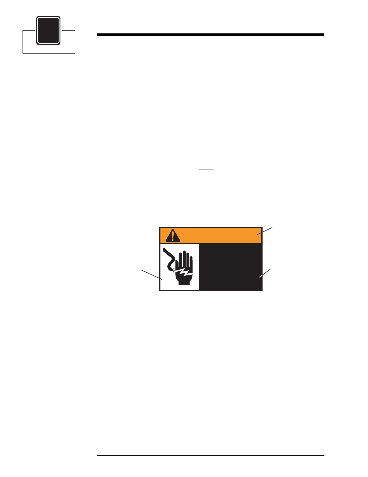
Crown Broadcast assumes the responsibility for providing you a safe product and
safety guidelines during its use. “Safety” means protection to all individuals who
install, operate, and service the transmitter as well as protection of the transmitter
itself. To promote safety, we use standard hazard alert labeling on the product and
in this manual. Follow the associated guidelines to avoid potential hazard.
1.5.1 Dangers
DANGER represents the most severe hazard alert. Extreme bodily harm or death
will occur if DANGER guidelines are not followed.
1.5.2 Warnings
WARNING represents hazards which could result in severe injury or death.
1.5.3 Cautions
CAUTION indicates potential personal injury or equipment or property damage if
the associated guidelines are not followed. Particular cautions in this text also
indicate unauthorized radio-frequency operation.
Pictorial Indication
of Hazard
WARNING
Severe shock hazard!
Turn power off and
wait approximately 1
minute for capacitors
to discharge before
handling them.
Illustration 1–5 Sample Hazard Alert
Type of Hazard
Explanation of
Hazard
1–10
FM500 User's Manual
Page 17
®
Section 2—Installation
This section provides important guidelines for installing your transmitter. Review this information carefully for proper installation.
Installation
2–1
Page 18
CAUTION
Possible equipment damage!
Before operating the transmitter for
the first time, check for the proper AC
line voltage setting and frequency
selection as described in sections 2.3
and 2.4.
2.1 Operating Environment
You can install the FM transmitter in a standard component rack or on a suitable
surface such as a bench or desk. In any case, the area should be as clean and wellventilated as possible. Always allow for at least 2 cm of clearance under the unit for
ventilation. If you set the transmitter on a flat surface, install spacers on the
bottom cover plate. If you install the transmitter in a rack, provide adequate
clearance above and below. Do not locate the transmitter directly above a hot piece
of equipment.
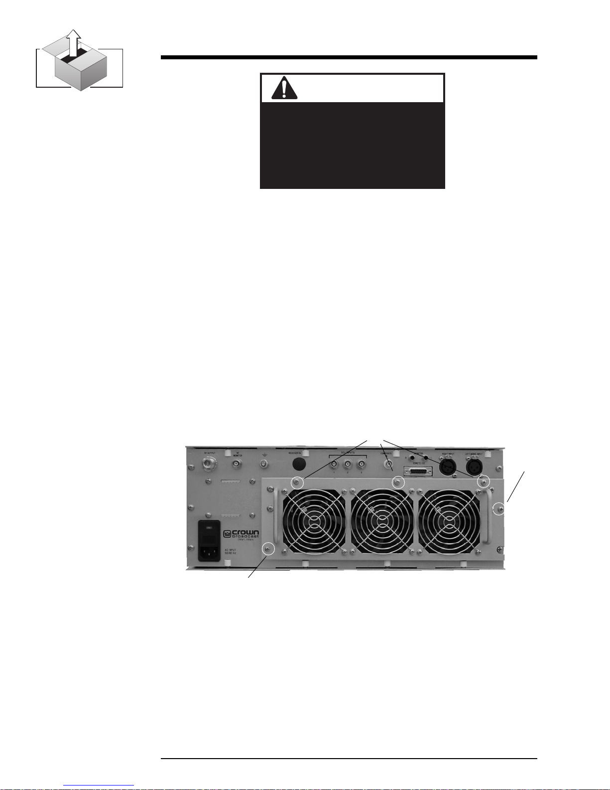
2.2 Remove PA Tray Spacers
The Crown FM 500 is shipped with spacers between the PA tray and the transmitter
back panel. The spacers prevent damage to internal contacts during shipping.
Remove and save the spacers and screws before installing the FM500.
#8
#8
#6
Illustration 2-1 FM 500 PA Tray Mounting Screws
1. Remove screws and spacers from five locations.
2. Firmly push the PA tray into the FM 500 until the PA tray panel touches the
back panel.
3. Locate the bag labeled 500 Hardware. Install four #8 screws and washers and
one number #6 screw and washer. See photo for locations.
2–2
FM500 User's Manual
Page 19
2.3 Power Connections
The FM500 operates on 100, 120, 220, or 240 volts AC (50 or 60 Hz; single phase).
As shipped (factory default settings), the FM500 operates on 120 volts at 60 Hz.
If you are operating the transmitter at 120 volts you do not need to make any
changes. To operate the FM500 at 100, 220, or 240 volts, a few changes are
necessary.
To change the voltage setting, follow these steps:
1. Disconnect the power cord if it is attached.
2. To set the input voltage for 100 volts, skip to step 7.
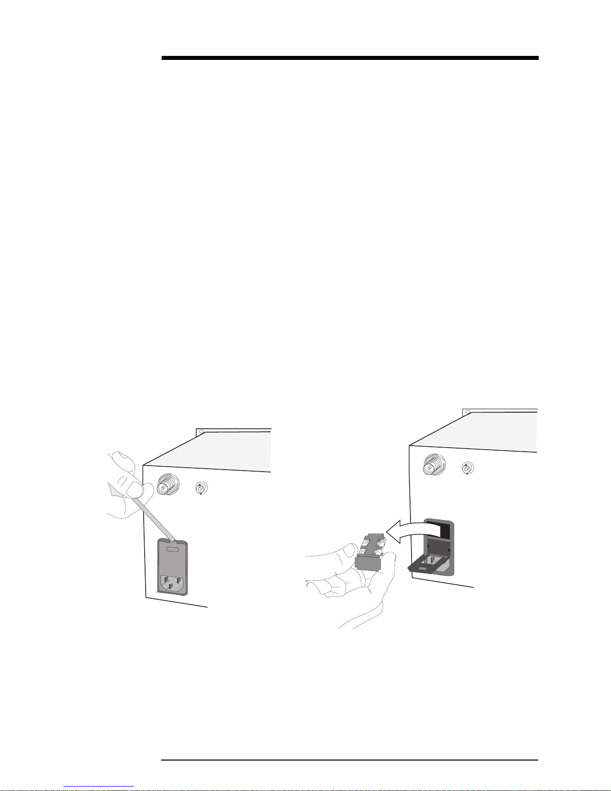
3. Open the cover of the power connector assembly using a small, flat blade
screwdriver. See Illustration 2–2.
4. Insert the screwdriver into the top slot of the voltage selection assembly
(red) and pry out the assembly from the power connector.
5. If you are setting the input voltage for 220 or 240 volts, replace the installed
fuses with 12 amp fuses (included in your package). See Illustration 2–3.
6. Replace the red fuse assembly so that the "230V" setting appears right side up
in the window. Close the assembly window.
115V
Illustration 2–2
Opening the Power Connector Cover
Installation
115V
230V
Illustration 2–3
Removing the Voltage Selection (red) Assembly
2–3
Page 20
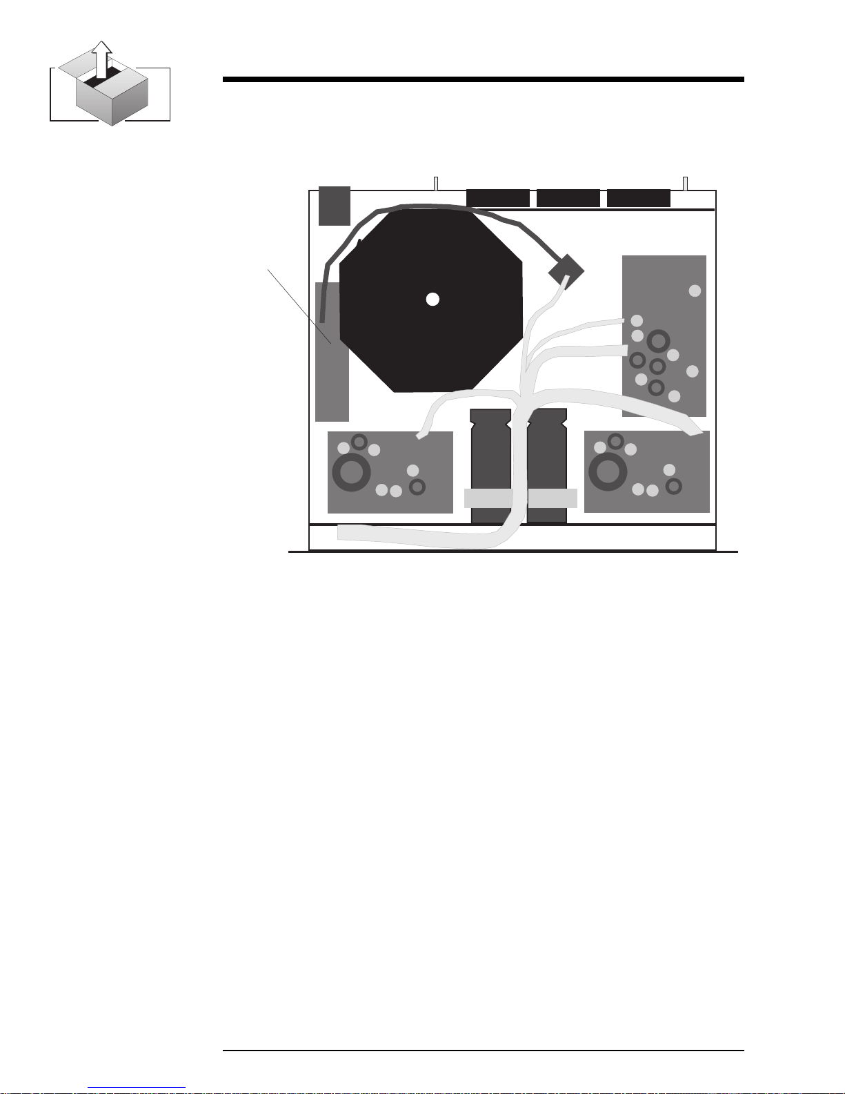
7. Turn the transmitter upside down and remove the bottom cover.
Note: The front panel filter grill must be removed to expose all of the bottom
Power
Distribution
Board
front of transmitter
Illustration 2–4 Underside of Transmitter—Bottom Cover Removed
cover screws for bottom cover removal and installation.
8. Locate the power distribution circuit board on the left side next to the large
transformer cover. See Illustration 2–4.
9. For 100 or 220 volt operation, change the jumper setting of P1 to the 100/
220 V setting.
10. For 220 or 240 volt operation,
• remove the jumper connecting P6 and P7.
• remove the jumper connecting P4 and P5.
• use a jumper to connect P5 and P6.
11. Replace the bottom cover, and the front grill.
12. Connect the AC power cord.
For your reference, use 12 amp fuses for 220 or 240 volt operation and 20 amp
fuses for 100 or 120 volt operation.
2–4
FM500 User's Manual
Page 21
2.4 Frequency (Channel) Selection
You may select an operating frequency of 87 to 108 MHz in the FM broadcast band
with 100 kHz channel spacing (10 kHz spacing is optional with the addition of a
fifth rotary selector switch).
To adjust the operating frequency, follow these steps:
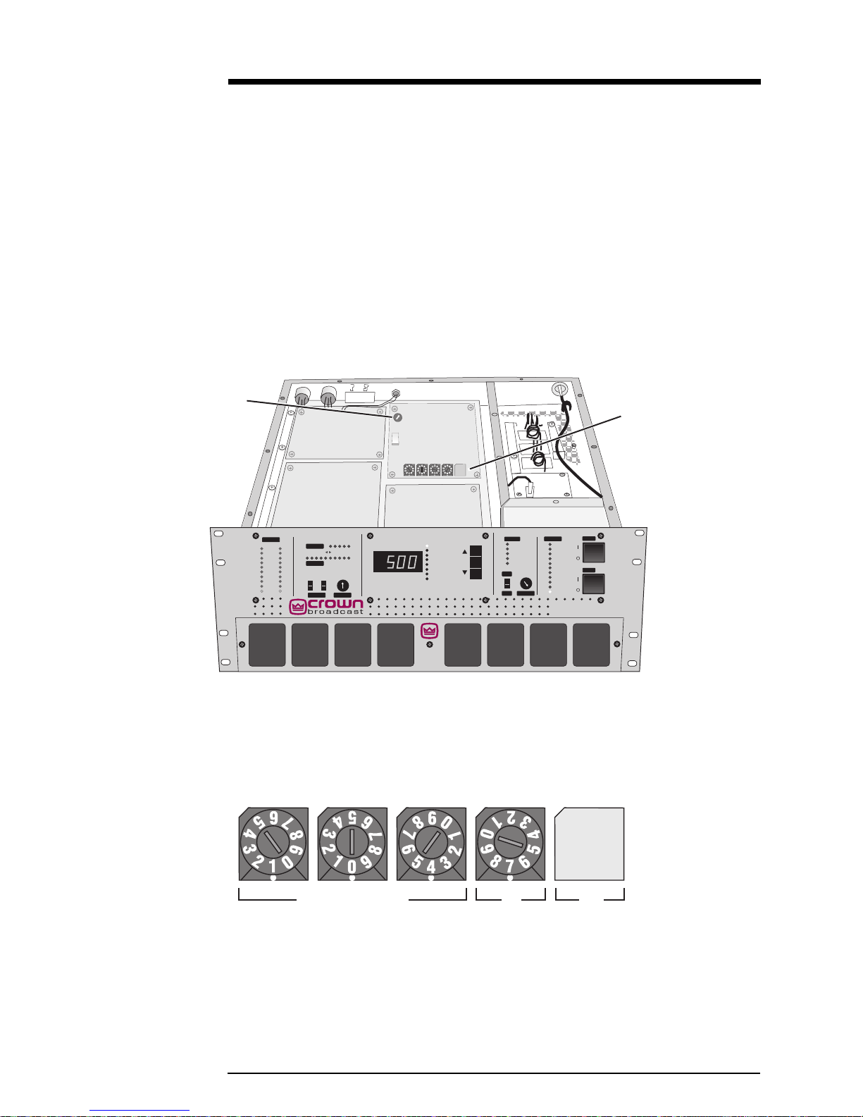
1. Remove the top cover by removing 15 screws.
2. Locate the RF Exciter board and identify the frequency selector switches
which will be used to change the setting. See Illustrations 2–5 and 2–6.
Modulation
Trim-pot
Audio Input
Frequency Selection
Rotary Switches
RF Exciter
10
High
-6
-12
-18
Low
2
+6 dB
Wide Band
Expand
Compress
20
+12 dB
ProcessingInput Gain
®
2
High Band
RF Power
SWR
ALC
PA DC Volts
PA DC Amps
PA Temperature
Supply DC Volts
Voltmeter
Fault
SWR
Lock
Input
PA DC
PA Temp
Stereo
Mono RF Output
Over
100
90
80
70
60
Power
50
40
30
20
Pilot
FM500
FM BROADCAST TRANSMITTER
Carrier
Modulation
Illustration 2–5 Top Cover Removed
Illustration 2–6 RF Exciter Board Frequency Selector Switches
Installation
MEGAHERTZ
.1 .01
2–5
Page 22
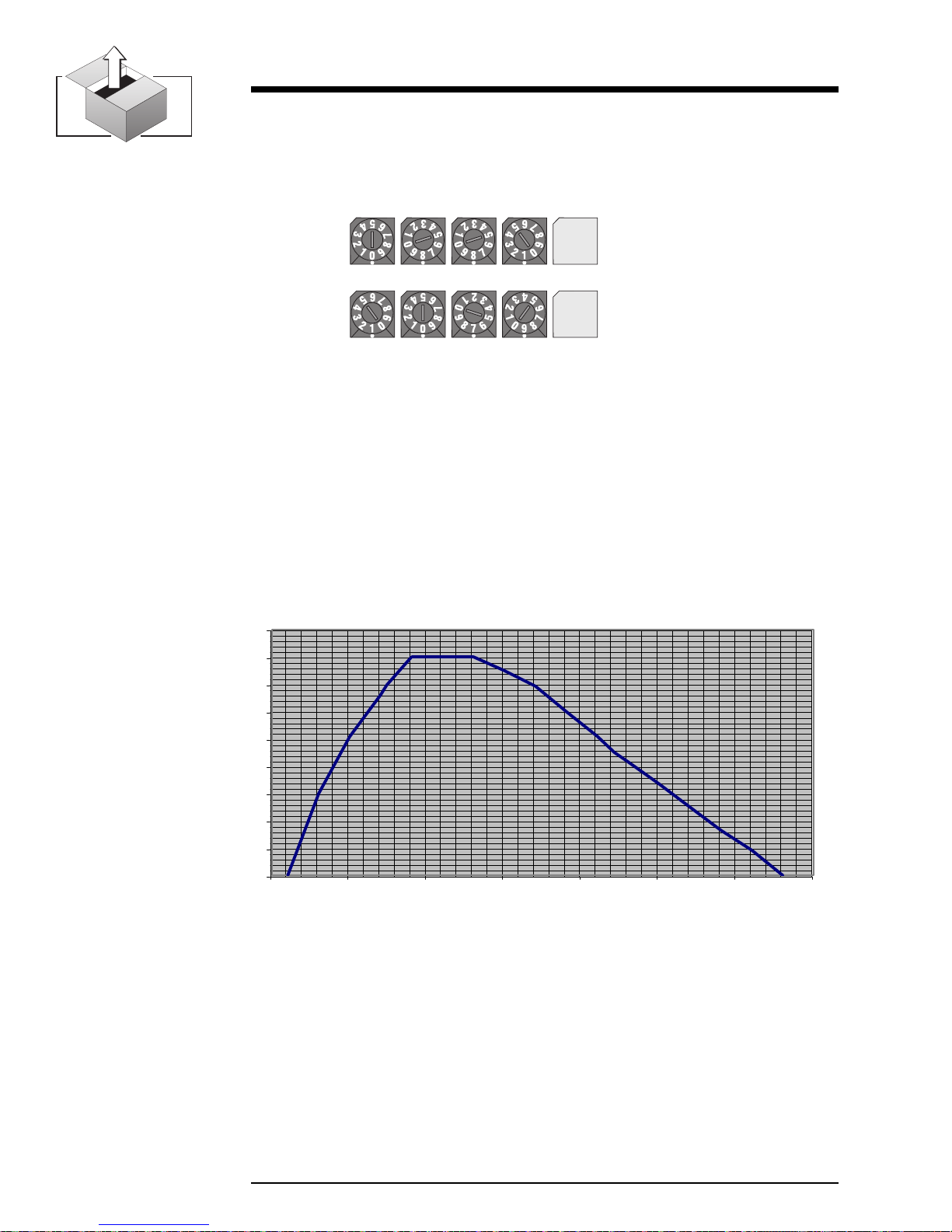
3. Use small flat blade screwdriver or another suitable device to rotate the
switches to the desired setting. (The selected number will appear directly
above the white indicator dot on each switch.) See examples of selected
frequencies in the illustration below.
= 88.1 MHz
= 107.9 MHz
Illustration 2–7 Two Sample Frequency Selections
4. If you have the receiver option, proceed to section 2.5 to set the incoming
frequency. Otherwise, replace the top cover.
2.4.1 Modulation Compensator
The Modulation trim-potentiometer (see illustration 2–8) compensates for slight
variations in deviation sensitivity with frequency. Set the trim-pot dial according
to the following graph:
Modulation Compensation Pot Setting
90
80
70
60
50
40
30
20
10
0
75 80 85 90 95 100 105 110
Frequency (MHz)
Illustration 2–8 Modulation Compensator Settings
These compensator settings are approximate. Each mark on the potentiometer
represents about 1.8% modulation compensation. For more exact settings, refer to
section 5.2.2.
2–6
FM500 User's Manual
Page 23

2.4.2 RF Tuning Adjustments
All the RF stages are broadband to cover the 88 to 108 MHz broadcast band. The
RF amplifier stages require no tuning.
2.5 Receiver Frequency Selection
If you have a transmitter equipped with the receiver option, you will need to set
the receiving or incoming frequency.
1. With the top cover removed, locate the receiver module and the two switches
(labeled SW1 and SW2).
2. Use the table on the following pages to set the switches for the desired
incoming frequency.
3. After setting the frequency, return to section 2.3.1 to set the modulation
compensator.
Frequency Selection
Switches SW1 & SW2
Stereo
Receiver
Generator
Module
Audio Input
High
-6
-12
-18
Low
2
High Band
Expand
Compress
2
Wide Band
+12 dB
+6 dB
Processing
Input Gain
Illustration 2–8 Receiver Module Switches
RF IN
RF Exciter
Carrier
Modulation
10
20
®
RF Power
SWR
ALC
PA DC Volts
PA DC Amps
PA Temperature
Supply DC Volts
Voltmeter
Fault
SWR
Lock
Input
PA DC
PA Temp
Stereo
Mono
RF Output
Over
100
90
80
70
60
Power
50
40
30
20
Pilot
FM500
FM BROADCAST TRANSMITTER
Installation
2–7
Page 24

Frequency S W1 SW2
87.9 0 0
88.0 80
88.1 0 1
88.2 8 1
88.3 0 2
88.4 8 2
88.5 0 3
88.6 8 3
88.7 0 4
88.8 8 4
88.9 0 5
89.0 85
89.1 0 6
89.2 8 6
89.3 0 7
89.4 8 7
89.5 0 8
89.6 8 8
89.7 0 9
89.8 8 9
89.9 0 A
90.0 8A
90.1 0 B
90.2 8 B
90.3 0 C
90.4 8 C
90.5 0 D
90.6 8 D
90.7 0 E
90.8 8 E
90.9 0 F
91.0 8F
91.1 1 0
91.2 9 0
91.3 1 1
91.4 9 1
91.5 1 2
91.6 9 2
91.7 1 3
91.8 9 3
91.9 1 4
92.0 94
92.1 1 5
92.2 9 5
92.3 1 6
92.4 9 6
92.5 1 7
92.6 9 7
92.7 1 8
92.8 9 8
92.9 1 9
Frequency SW1 SW2
93.0 99
93.1 1 A
93.2 9 A
93.3 1 B
93.4 9 B
93.5 1 C
93.6 9 C
93.7 1 D
93.8 9 D
93.9 1 E
94.0 9E
94.1 1 F
94.2 9 F
94.3 2 0
94.4 A 0
94.5 2 1
94.6 A 1
94.7 2 2
94.8 A 2
94.9 2 3
95.0 A3
95.1 2 4
95.2 A 4
95.3 2 5
95.4 A 5
95.5 2 6
95.6 A 6
95.7 2 7
95.8 A 7
95.9 2 8
96.0 A8
96.1 2 9
96.2 A 9
96.3 2 A
96.4 A A
96.5 2 B
96.6 A B
96.7 2 C
96.8 A C
96.9 2 D
97.0 AD
97.1 2 E
97.2 A E
97.3 2 F
97.4 A F
97.5 3 0
97.6 B 0
97.7 3 1
97.8 B 1
97.9 3 2
Frequency SW1 SW2
98.0 B2
98.1 3 3
98.2 B 3
98.3 3 4
98.4 B 4
98.5 3 5
98.6 B 5
98.7 3 6
98.8 B 6
98.9 3 7
99.0 B7
99.1 3 8
99.2 B 8
99.3 3 9
99.4 B 9
99.5 3 A
99.6 B A
99.7 3 B
99.8 B B
99.9 3 C
100.0 BC
100.1 3 D
100.2 B D
100.3 3 E
100.4 B E
100.5 3 F
100.6 B F
100.7 4 0
100.8 C 0
100.9 4 1
101.0 C1
101.1 4 2
101.2 C 2
101.3 4 3
101.4 C 3
101.5 4 4
101.6 C 4
101.7 4 5
101.8 C 5
101.9 4 6
102.0 C6
102.1 4 7
102.2 C 7
102.3 4 8
102.4 C 8
102.5 4 9
102.6 C 9
102.7 4 A
102.8 C A
102.9 4 B
Frequency SW1 SW2
103.0 CB
103.1 4 C
103.2 C C
103.3 4 D
103.4 C D
103.5 4 E
103.6 C E
103.7 4 F
103.8 C F
103.9 5 0
104.0 D0
104.1 5 1
104.2 D 1
104.3 5 2
104.4 D 2
104.5 5 3
104.6 D 3
104.7 5 4
104.8 D 4
104.9 5 5
105.0 D5
105.1 5 6
105.2 D 6
105.3 5 7
105.4 D 7
105.5 5 8
105.6 D 8
105.7 5 9
105.8 D 9
105.9 5 A
106.0 DA
106.1 5 B
106.2 D B
106.3 5 C
106.4 D C
106.5 5 D
106.6 D D
106.7 5 E
106.8 D E
106.9 5 F
107.0 DF
107.1 6 0
107.2 E 0
107.3 6 1
107.4 E 1
107.5 6 2
107.6 E 2
107.7 6 3
107.8 E 3
107.9 6 4
108.0 E4
2–8
Table 2–1 Receiver Frequency Selection
FM500 User's Manual
Page 25
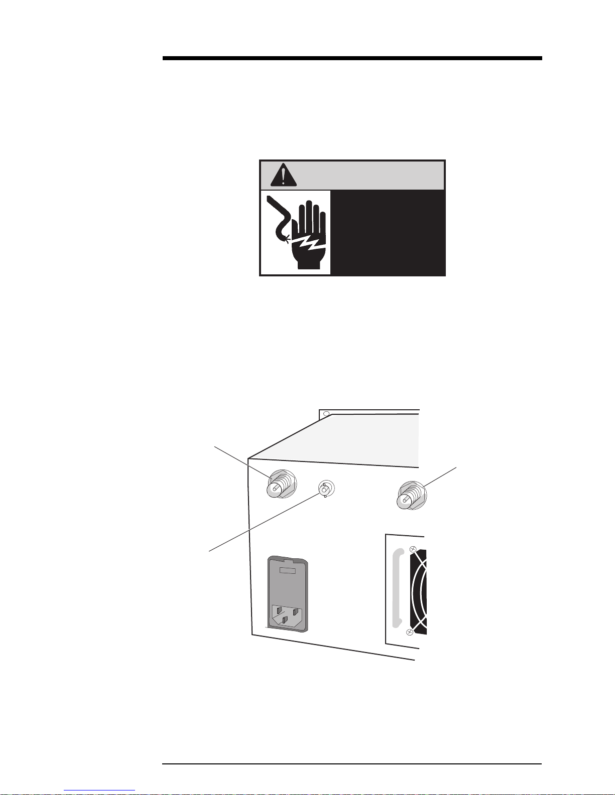
2.6 RF Connections
Connect the RF load, an antenna or the input of an external power amplifier, to
the type-N, RF output connector on the rear panel. VSWR should be 1.5:1 or
better.
WARNING
Severe shock hazard!
Do not touch the inner
portion of the RF
output connector
when transmitter
power is on.
The RF monitor is intended primarily for a modulation monitor connection.
Information gained through this connection can supplement that which is
available on the transmitter front panel displays.
If your transmitter is equipped with the receiver option, connect the incoming RF
to the RF IN connector.
RF Output
Connector
RF Output
Monitor
RFInput Connector
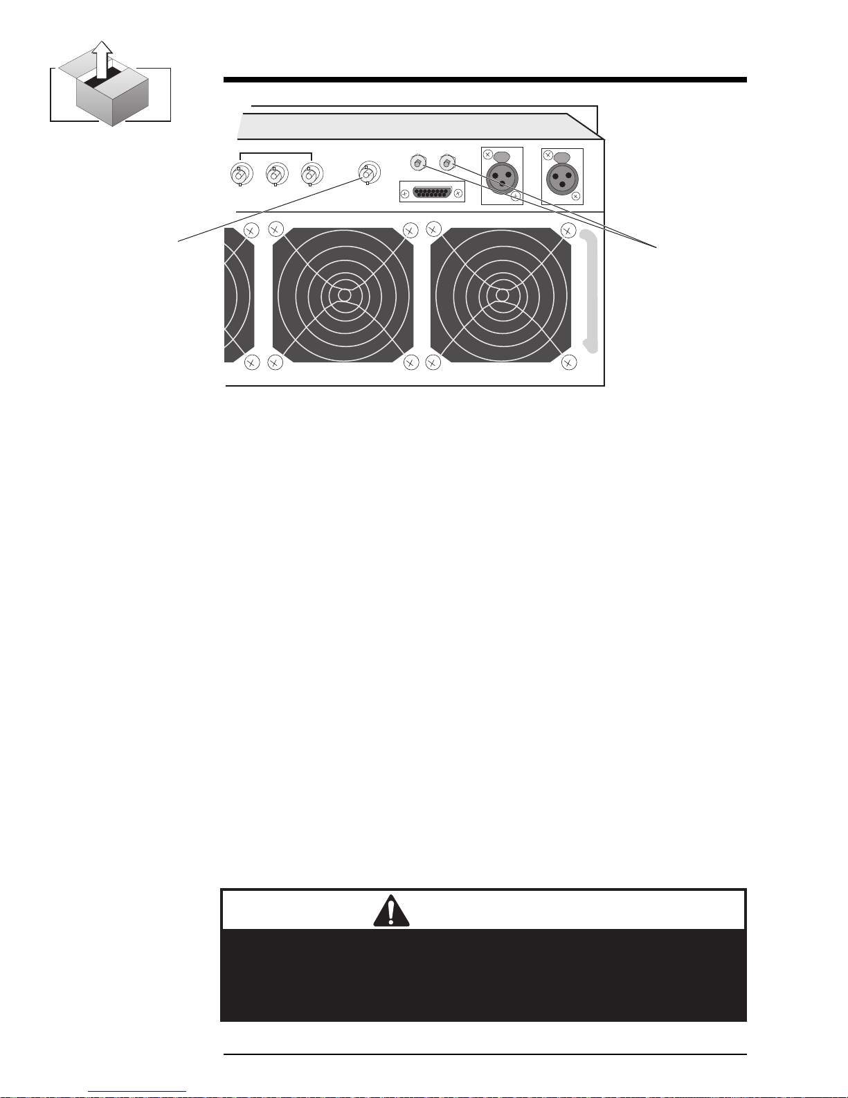
(receiver option only)
115V
Illustration 2–10 RF Connections
Installation
2–9
Page 26
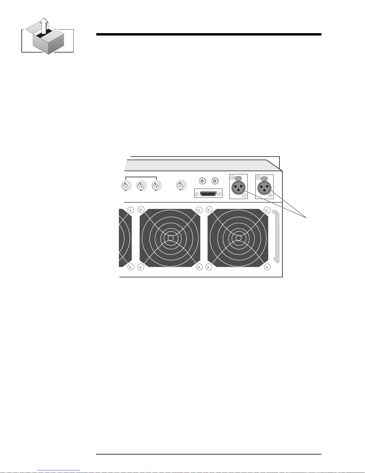
2.7 Audio Input Connections
Attach audio inputs to the Left and Right XLR connectors on the rear panel. (The
Left channel audio is used on Mono.) Pin 1 of the XLR connector goes to chassis
ground. Pins 2 and 3 represent a balanced differential input with an impedance of
about 50 kΩ. They may be connected to balanced or unbalanced left and right
program sources.
The audio input cables should be shielded pairs, whether the source is balanced or
unbalanced. For an unbalanced program source, one line (preferably the one
connecting to pin 3) should be grounded to the shield at the source. Audio will
then connect to the line going to pin 2.
SCA IN
1
23
COMPOSITE IN
R
MONITOR
REMOTE I/O
RIGHT
L
LEFT/MONO
Audio
Inputs
Illustration 2-10 XLR Audio Input Connectors
By bringing the audio return line back to the program source, the balanced
differential input of the transmitter is used to best advantage to minimize noise.
This practice is especially helpful if the program lines are fairly long but is a good
practice for any distance.
If the program source requires a 600 Ω termination, install resistors on the 8–pin
DIP socket on the motherboard (socket A501 located between the XLR
connectors). See the motherboard schematic, on page 6–13.
2–10
FM500 User's Manual
Page 27
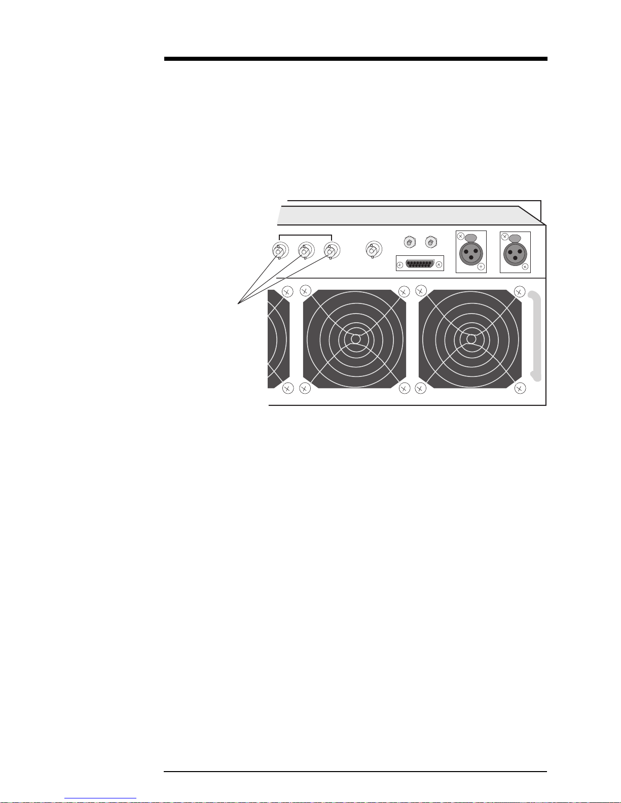
2.8 SCA Input Connections
You can connect external SCA generators to the SCA In connectors (BNC-type) on
the rear panel. The inputs are intended for the 60 kHz to 99 kHz range, but a
lower frequency may be used if the transmitter is operated in Mono mode. (The 23
to 53 kHz band is used for stereo transmission.) For 7.5 kHz deviation (10%
modulation), input of approximately 3.5–volts (peak-to-peak) is required.
SCA IN
1
23
COMPOSITE IN
R
MONITOR
REMOTE I/O
RIGHT
L
LEFT/MONO
SCA Inputs
(BNC) Connectors
Illustration 2–12 SCA Input Connectors
2.9 Composite Input Connection
To use the Crown transmitter as an RF Exciter only ("E" version or when using the
"T" version with composite input), it is necessary to use the Composite Input
section of the transmitter. This will feed composite stereo (or mono audio) directly
to the RF exciter. In the "T" version, this will bypass the internal audio processor
and stereo generator. See Section 2.12 on the next page for caution in using the
bypass option.
Input sensitivity is approximately 3.5–volt P-P for 75 kHz deviation.
1. Enable the Composite Input by grounding pin 9 of the Remote I/O connector
(see Illustration 2–15).
2. Connect the composite signal using the Composite In BNC connector.
Installation
2–11
Page 28
SCA IN
1
23
COMPOSITE IN
R
MONITOR
REMOTE I/O
RIGHT
L
LEFT/MONO
Composite Input
(BNC) Connector
Audio Monitor
(RCA) Jacks
Illustration 2–13 Composite In and Audio Monitor Connections
2.10 Audio Monitor Connections
Processed, de-emphasized samples of the left and right audio inputs to the stereo
generator are available at the Monitor jacks on the rear panel. The signals are
suitable for feeding a studio monitor and for doing audio testing. De-emphasis is
normally set for 75 µsec; set to 50 µsec by moving jumpers, JP203 and JP204, on
the Stereo Generator board.
2.11 Pre-emphasis Selection
Select the pre-emphasis curve (75 µsec, 50 µsec, 25 µsec, or Flat) by jumpering the
appropriate pins of header JP1 on the audio processor board. If you change the
pre-emphasis, change the de-emphasis jumpers JP203 and JP204 on the Stereo
Generator board to match.
2.12 Processor Bypass Option
You may bypass the audio processor in order to feed the left and right (preemphasized) audio directly to the stereo generator. The Normal-Bypass slide
switch is near the left-rear corner of the motherboard. If the audio source is
already processed and you do not desire further processing, use the Normal mode
but turn the Processing control (on the front panel) to “0.” (See also section 3.5.)
CAUTION
In the BYPASS position, the pre-emphasis circuits and the filters that protect the
pilot and stereo subcarrier are bypassed. As a result, the occupied bandwidth
specifications of the transmitter could be compromised. The 15–Hz high-pass
filters are also bypassed which may mean that modulation with frequencies
below 10 Hz could cause the frequency synthesizer to unlock.
2–12
FM500 User's Manual
Page 29
2.13 Program Input Fault Time-out
You can enable an automatic turn-off of the carrier in the event of program failure.
To enable this option, see the table on the next page. The time between program
failure and carrier turn-off is set by a jumper (JP701) on the voltage regulator
board (see Illustration 6–4 for board location). Jumper pins 1 and 2 (the two pins
closest to the edge of the board) for a delay of approximately 30 seconds; pins 3 and
4 for a 2–minute delay; pins 5 and 6 for a 4–minute delay, and pins 7 and 8 for an
8–minute delay.
2.14 Remote I/O Connector
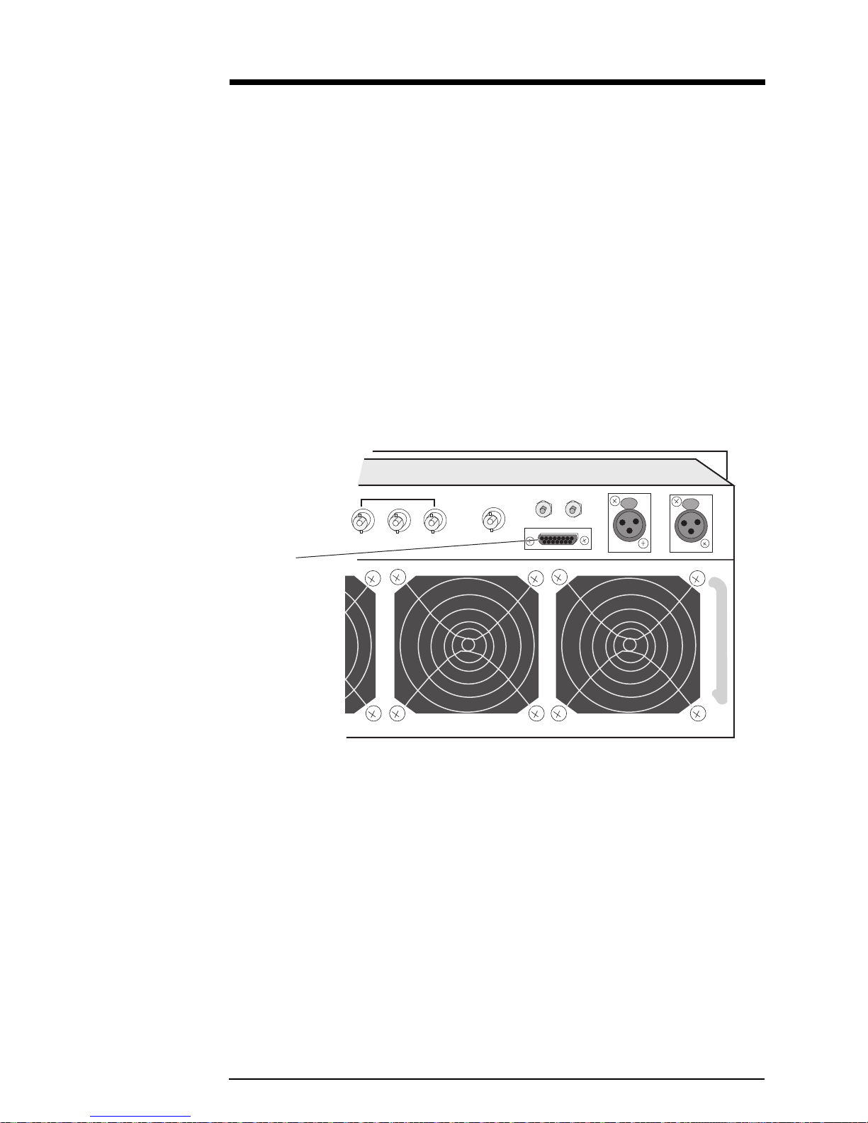
Remote control and remote metering of the transmitter is made possible through a
15–pin, D-sub connector on the rear panel. (No connections are required for
normal operation.)
SCA IN
1
23
COMPOSITE IN
MONITOR
R
REMOTE I/O
RIGHT
L
Remote I/O
Illustration 2–14 Remote I/O Connector
The following table summarizes the Remote I/O pin connections.
LEFT/MONO
Installation
2–13
Page 30

Pin Number Function
1 Ground
2 (no connection)
3 Composite Out (sample of stereo generator output)
4 FSK In (Normally high; pull low to shift carrier
frequency approximately 7.5 kHz. Connect to open
collector or relay contacts of user-supplied FSK keyer.)
5 /Auto Carrier Off (Pull low to enable automatic turnoff
of carrier with program failure.)
6 Meter Battery (unregulated DC volts; 5 volts = 50 VDC)
7 Meter RF Watts (1 volt = 100 watts)
8 Meter PA Volts (5 volts = 50 VDC)
9 /Ext. Enable (Pull low to disable internal stereo
generator and enable External Composite Input.)
10 a) 38 kHz Out (From stereo generator for power supply
synchronization.)
b) For transmitters equipped with tuner option, this pin
becomes the right audio output for an 8–ohm monitor
speaker. 38kHZ Out is disabled.
11 ALC
12 /Carrier Off (pull low to turn carrier off.)
13 Fault Summary (line goes high if any fault light is
activated.)
14 Meter PA Temperature (5 volts = 100 degrees C.)
15 Meter PA Current (1 volt = 10 amperes DC.)
Table 2–3 Remote I/O Connections
8
15
1
9
Illustration 2–15 Remote I/O Connector (outside view)
2–14
FM500 User's Manual
Page 31
Section 3—Operation
This section provides general operating parameters of your
transmitter and a detailed description of its front panel display .
Operation
3–1
Page 32
3.1 Initial Power-up Procedures
These steps summarize the operating procedures you should use for the initial
operation of the transmitter . More detailed information follows.
CAUTION
Possible equipment damage!
Before operating the transmitter for
the first time, check for the proper AC
line voltage setting and frequency
selection as described in sections 2.3
and 2.4.
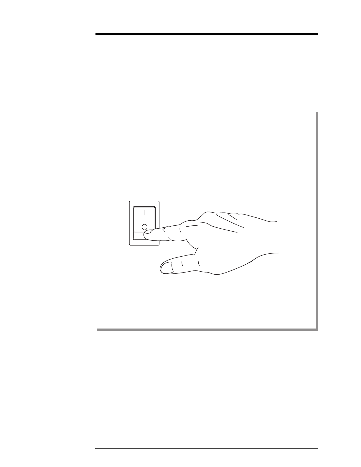
1. Turn on the main power switch.
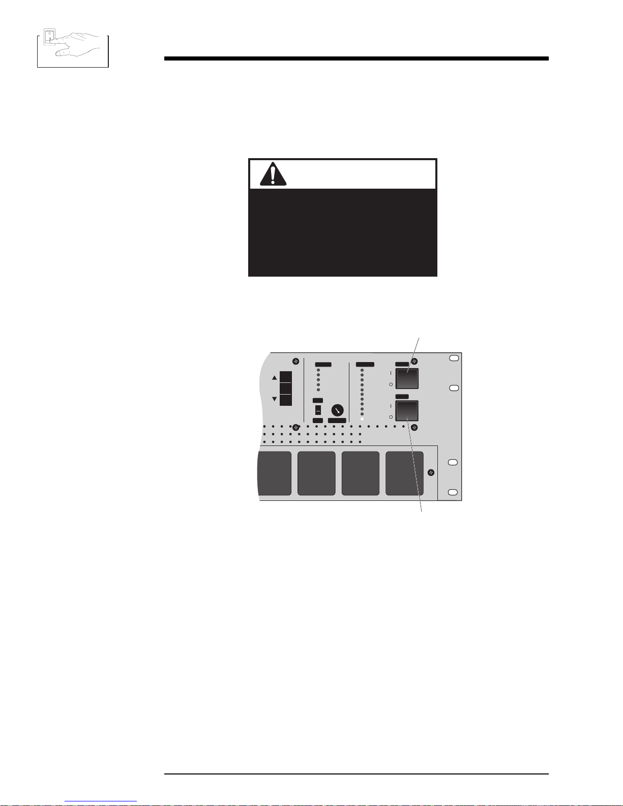
Carrier Switch
Fault
SWR
Lock
Input
PA DC
PA Temp
Stereo
Mono RF Output
Modulation
Over
100
90
80
70
60
50
40
30
20
Pilot
FM500
FM BROADCAST TRANSMITTER
Carrier
Power
Power Switch
Illustration 3–1 Front Panel Power Switches
2. Verify the following:
a. The bottom cooling fans runs continuously.
b. The Lock Fault indicator flashes for approximately 5 seconds, then goes
off.
4. Set the Input Gain switches for mid-scale wideband gain reduction on an
average program level (see section 3.4).
5. Set the Processing control (see section 3.5; normal setting is “50”).
6. Set the Stereo-Mono switch to Stereo (see section 3.6).
7. Turn on the Carrier switch.
3–2
FM500 User's Manual
Page 33

8. Check the following parameters on the front panel multimeter:
a. RF Power should be 500–550 watts.
b. SWR should be less than 1.25 (A reading greater than 1.25 indicates an
antenna mismatch).
c. ALC should be between 4.00 and 6.00 volts.
d. PA DC Volts should be 46–56 volts. (Varies with antenna match, power,
and frequency.)
e. PA DC Amperes should be 12–16 amps. (Varies with antenna match,
power , and frequency.)
f. PA Temperature should initially read 20–35 degrees C (room tempera-
ture). After one hour the reading should be 35–50 degrees C.
g. Supply DC Volts should display a typical reading of 65–70 V with the
carrier on and 80–85 V with the carrier off
h. Voltmeter should be reading 0.0.
The remainder of this section describes the functions of the front panel indicators
and switches.
Operation
3–3
Page 34
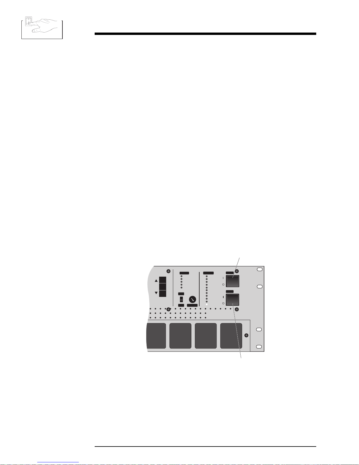
3.2 Power Switches
3.2.1 DC Breaker
The DC breaker , on the rear panel, must be on (up) for transmitter operation, even
when using AC power . Electrically, the DC breaker is located immediately after
diodes which isolate the DC and AC power supplies.
3.2.2 Power Switch
The main on/off power switch controls both the 120/240 VAC and the DC battery
power input.
3.2.3 Carrier Switch
This switch controls power to the RF amplifiers and supplies a logic high to the
voltage regulator board, which enables the supply for the RF driver. In addition,
the Carrier Switch controls the operating voltage needed by the switching power
regulator .
A "Lock Fault" or a low pin 12 (/Carrier Off) on the Remote I/O connector will hold
the carrier off. (See section 2.12.)
Carrier Switch
Fault
SWR
Lock
Input
PA DC
PA Temp
Stereo
Mono RF Output
Modulation
Over
100
90
80
70
60
50
40
30
20
Pilot
FM500
Carrier
Power
FM BROADCAST TRANSMITTER
Power Switch
Illustration 3–2 Front Panel Power Switches
3–4
FM500 User's Manual
Page 35

3.3 Front Panel Bar-Dot Displays
Bar-dot LEDs show audio input levels, wideband and highband audio gain control, and
modulation percentage. Resolution for the gain control and modulation displays is
increased over a conventional bar-graph display using dither enhancement which
modulates the brightness of the LED to give the effect of a fade from dot to dot. (See
section 4.7.)
3.3.1 Audio Processor Input
T wo vertical, moving-dot displays for the left and right channels indicate the relative
audio levels, in 3 dB steps, at the input of the audio processor . Under normal operating conditions, the left and right Audio Processor indicators will be active, indicating
the relative audio input level after the Input Gain switches. During program pauses,
the red Low LED will light.
With the receiver module option installed, the audio processor indicators are disabled.
3.3.2 Highband and Wideband Display
During audio processing, the moving-dot displays indicate the amount of gain control
for broadband (Wide) and pre-emphasized (High) audio. These indicators are disabled
if the receiver module option is installed.
As long as program material causes activity of the Wideband green indicators, deter mined by the program source level and Input Gain switches, the transmitter will be
fully modulated. (See section 3.4.)
The Wideband indicator shows short-term “syllabic-rate” expansion and gain reduction
around a long-term (several seconds) average gain set.
Program material and the setting of the Processing control determine the magnitude
of the short-term expansion and compression (the rapid left and right movement of the
green light).
High-frequency program content affects the activity of the Highband indicator . With
75–µsec pre-emphasis, Highband processing begins at about 2 kHz and increases as the
audio frequency increases. Some programs, especially speech, may show no activity
while some music programs may show a great deal of activity.
3.3.3 Modulation Display
A 10–segment, vertical peak-and-hold, bar graph displays the peak modulation percentage. A reading of “100” coincides with 75 kHz deviation. The display holds briefly
(about 0.1 seconds) after the peak. The “Pilot” indicator illuminates when the transmitter is in the stereo mode.
T o verify the actual (or more precise) modulation percentage, connect a certified
modulation monitor to the RF monitor jack on the rear panel.
Operation
3–5
Page 36
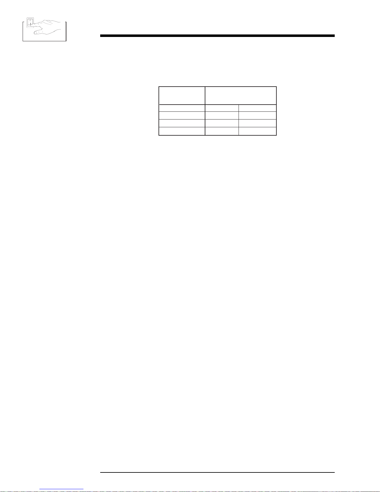
3.4 Input Gain Switches
The “+6 dB” and “+12 dB” slide switches set audio input sensitivity according to the
following table.
Nominal Input Switches
Sensitivity +6 dB +12 dB
+10 dBm Down Down
+4 dBm Up Down
-2 dBm Down Up
-8 dBm Up Up
Table 3–1 Input Gain Switches
Find, experimentally, the combination of Input Gain switch settings that will bring
the Wideband gain-reduction indicator to mid scale for “normal” level program
material. The audio processor will accommodate a fairly wide range of input levels
with no degradation of audio quality.
3.5 Processing Control
T wo factors contribute to the setting of the Processing control: program material
and personal taste. For most program material, a setting in the range of 40 to 70
provides good program density . For the classical music purist, who might prefer
preservation of music dynamics over density, 10 to 40 is a good range. The audio
will be heavily processed in the 70 to 100 range.
If the program source is already well processed, as might be the case with a satellite
feed, set the Processing to “0” or “10”.
3.6 Stereo-Mono Switch
The Stereo-Mono slide switch selects the transmission mode. In Mono, feed audio
only to the left channel. Although right-channel audio will not be heard as audio
modulation, it will affect the audio processing.
3–6
FM500 User's Manual
Page 37
3.7 RF Output Control
Set this control for the desired output power level. Preferably , set the power with an
external RF wattmeter connected in the coaxial line to the antenna. You may also use
the RF power reading on the digital multimeter .
The control sets the RF output voltage. Actual RF output power varies as the approximate square of the relative setting of the control. For example, a setting of “50” is
approximately 1/4 full power . Operation below 100 watts is not recommended as
instability can occur which could damage the transmitter .
CAUTION
Possible equipment damage!
Operation below 100 watts can cause
oscillations and other problems that
could damage the transmitter.
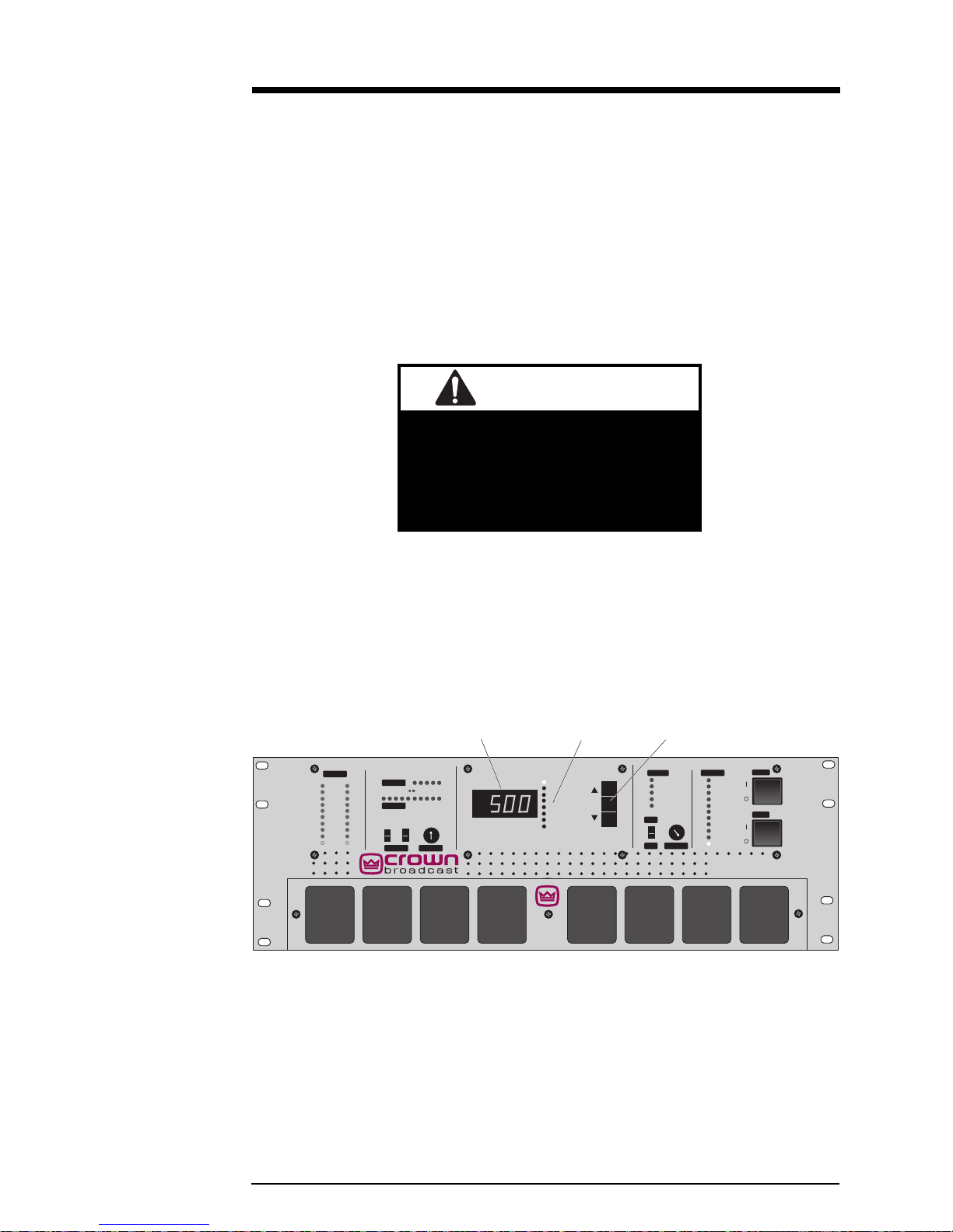
3.8 Digital Multimeter
The four-digit numeric display in the center of the front panel provides information
on transmitter operation. Use the “Up” and “down” push-buttons to select one of
the following parameters. A green LED indicates the one selected.
Audio Input
High
-12
-18
Low
Digital Multimeter Multimeter Functions
10
2
High Band
Expand
Compress
2
-6
Wide Band
+6 dB
20
+12 dB
ProcessingInput Gain
®
RF Power
SWR
ALC
PA DC Volts
PA DC Amps
PA Temperature
Supply DC Volts
Voltmeter
Illustration 3–3 Digital Multimeter
Multimeter Push-buttons
Fault
SWR
Lock
Input
PA DC
PA Temp
Stereo
Mono RF Output
Modulation
Carrier
Over
100
90
80
70
60
Power
50
40
30
20
Pilot
FM500
FM BROADCAST TRANSMITTER
RF Power—Actually reads RF voltage squared, so the accuracy can be affected by
VSWR (Voltage Standing-Wave Ratio). See section 5.4 for calibration. Requires
calibration with the RF reflectometer being used.
SWR—Direct reading of the antenna standing-wave ratio (the ratio of the desired
load impedance, 50 ohms, to actual load).
Operation
3–7
Page 38

ALC—DC gain control bias used to regulate PA supply voltage. With the P A power
supply at full output voltage, ALC will read about 6.0 volts. When the RF output is
being regulated by the RF power control circuit, this voltage will be reduced, typically reading 4 to 5.5 volts. The ALC voltage will be reduced during PA DC
overcurrent, SWR, or LOCK fault conditions.
PA DC V olts—Supply voltage of the RF power amplifier.
PA DC Amps—Transistor drain current for the RF power amplifier.
PA DC Temperature—T emperature of the RF power amplifier heatsink in degrees C.
Supply DC Volts—Unregulated DC voltage at the input of the voltage regulators. For
battery operation, this reading is the battery voltage minus a diode drop.
Voltmeter—Reads the voltage at a test point located on the front edge of the mother-
board. A test lead connected to this point can be used for making voltage measurements in the transmitter . The test point is intended as a servicing aid; an alternative
to an external test meter . Remember that the accuracy is only as good as the reference voltage used by the metering circuit. Servicing a fault affected by the reference
affects the Voltmeter reading. The metering scale is 0 to 199.9 volts.
3.9 Fault Indicators
Faults are indicated by a blinking red light as follows:
SWR—Load VSWR exceeds 1.5:1. ALC voltage is reduced to limit the reflected RF
power.
Lock—Frequency synthesizer phase-lock loop is unlocked. This indicator normally
blinks for about five seconds at power turn-on. Whenever this light is blinking,
supply voltages will be inhibited for the RF driver stage as well as for the RF power
amplifier .
Input—The automatic carrier-off circuit is enabled (see sections 2.11 and 2.12) and
the absence of a program input signal has exceeded the preset time. (The circuit
treats white or pink noise as an absence of a program.)
PA DC—Power supply current for the RF power output amplifier is at the preset
limit. ALC voltage has been reduced, reducing the PA supply voltage to hold supply
current to the preset limit.
PA Temp—PA heatsink temperature has reached 80–85° C (178–185° F).
At about 83° C (181°F), ALC voltage begins to decrease, reducing the PA supply
voltage to prevent a further increase in temperature. By 85° C (185° F), the PA will
be fully cut off.
3–8
FM500 User's Manual
Page 39

p
u
e
d
e
r
o
s
n
o
n
o
e
r
e
c
h
do,
n
o
m
o
t
s
e
u
q
n
ce
i
i
d
i
s
o
n
u
,
e
s
r
ch
o
f
e
h
c
o
m
a
i
c
i
d
e
s
con
o
d
n
e
v
i
r
c
s
a
m
do,
n
o
m
o
t
s
e
u
q
n
ce
i
i
d
i
s
o
n
u
,
e
s
r
ch
o
f
e
h
c
o
m
a
i
c
i
d
e
s
con
o
d
n
e
v
i
r
c
s
a
m
con
o
d
n
e
v
i
r
c
s
a
m
do,
n
o
m
o
t
s
e
u
q
n
ce
i
i
d
i
s
o
n
u
,
e
s
r
o
f
e
h
c
o
m
a
i
c
i
d
e
s
o
c
o
d
n
e
v
i
r
c
s
a
m
e
a
b
b
i
a
n
n
o
n
e
h
c
c
n
o
n
e
t
i
t
a
m
a
l
d
o
n
o
r
e
n
o
n
e
h
c
c
n
o
n
e
t
i
t
a
m
a
l
a
m
a
l
o
n
o
r
e
o
n
e
h
c
n
o
n
e
ch
ati
m
a
l
n
o
h
a
l
a
d
i
s
p
o
z
i
o
n
e
d
o
f
a
'
e
n
u
l
l
a
n
e
l
m
o
n
d
o
r
e
a
l
e
a
c
i
i
n
s
e
g
n
a
a
n
o
n
p
a
r
l
p
u
e
e
r
s
o
n
e
c
h
e
a
b
b
i
a
n
h
a
l
a
d
i
s
p
o
z
i
o
n
e
d
o
f
a
'
e
n
u
l
l
a
n
e
l
m
o
n
d
o
r
e
a
l
e
a
c
i
i
n
s
e
g
n
a
a
n
o
n
p
a
r
l
t
a
c
i
i
i
t
n
s
e
g
n
a
a
n
o
n
p
a
p
u
e
d
e
r
s
o
n
e
c
h
e
a
b
b
i
a
n
h
a
l
a
d
i
s
p
o
z
i
o
n
e
d
o
f
'
e
n
u
c
l
l
a
n
e
l
m
o
n
d
o
r
e
a
t
a
c
i
i
n
s
e
g
n
a
a
n
o
n
p
a
m
r
l
o
.
M
n
i
d
i
o
f
a
r
e
o
r
l
o
s
.
M
d
i
m
a
r
e
s
m
r
l
a
r
e
n
o
a
r
l
o
.
M
l
e
d
i
r
l
a
re
t
a
c
i
i
i
t
n
s
a
e
m
g
n
a
l
a
a
con
o
d
n
e
v
i
r
c
s
a
do,
n
o
m
o
t
s
e
u
q
ce
i
d
i
s
o
n
u
,
e
s
r
ch
e
h
c
o
m
a
i
c
i
d
e
con
o
d
n
e
v
i
r
c
s
a
ch
e
h
c
o
m
a
i
c
i
d
e
con
o
d
n
e
v
i
r
c
s
a
n
o
n
p
a
r
l
a
r
e
p
u
e
d
e
r
o
s
n
o
n
o
e
r
e
c
h
e
a
b
b
i
a
n
n
o
n
e
h
c
'
c
n
o
n
e
t
a
i
t
a
m
a
l
'
c
n
o
n
e
t
a
i
t
a
m
a
l
o
h
a
l
a
d
i
s
p
o
z
i
o
n
e
d
o
f
a
r
l
o
.
M
e
n
u
l
l
a
n
e
l
m
o
n
d
o
r
e
a
l
e
d
c
e
c
i
i
i
n
s
e
g
n
a
a
n
o
n
p
a
r
l
a
r
e
n
u
l
l
a
n
e
l
m
o
n
d
o
r
e
a
l
e
d
i
i
i
n
s
e
g
n
a
a
n
o
n
p
a
r
l
a
r
e
Section 4—Principles of Operation
This section discusses the circuit principles upon which the
transmitter functions. This information is not needed for day-today operation of the transmitter but may be useful for advanced
users and service personnel.
Principles of Operation
4–1
Page 40

m
o
t
o
s
n
n
d
e
e
u
q
o
s
n
i
u
n
,
i
e
s
r
o
m
c
a
o
i
f
c
i
d
e
n
e
d
v
o
i
s
r
c
s
a
m
o
t
o
s
m
e
u
q
o
s
n
i
u
n
,
i
e
s
r
o
m
c
h
a
o
i
f
c
i
d
e
n
e
d
v
o
i
s
r
c
s
a
m
n
e
d
v
i
r
c
s
a
m
o
t
o
s
m
e
u
q
o
s
n
i
u
n
,
i
e
s
r
o
m
c
a
o
i
f
c
i
d
e
n
e
d
v
i
s
r
c
s
a
m
d
v
o
i
r
o
d
i
c
e
h
e
c
o
n
d
o
d
i
c
e
e
c
o
o
c
o
n
d
d
i
c
h
e
o
c
o
c
c
o
s
,
n
,
n
n
o
,
e
n
n
a
m
o
t
o
s
n
m
d
e
o
u
,
q
o
s
n
i
u
d
,
i
in
c
e
e
s
r
o
f
o
m
c
h
a
e
ci
i
d
e
n
e
d
v
o
i
s
r
c
c
o
s
n
a
o
m
c
h
a
m
i
e
c
i
d
e
n
e
d
v
o
i
s
r
c
c
o
s
n
a
m
4.1 Part Numbering
As this section refers to individual components, you should be familiar with the
part numbering scheme used. Although parts on the various circuit boards and
circuit board drawings may be marked with identical reference numbers, each
component in the transmitter has a unique part reference number.
The circuit boards and component placement drawings use designators such as
“R1”, “R2”, and “C1.” These numbers represent only a portion of the full part
numbers (as shown on the schematic). To find the full number, refer to the chart
below. R401, for instance, is marked “R1” on the Metering board and on its
component placement drawing.
Circuit Name Part numbers
Audio Processor 0-199
Stereo Generator 200’s
RF Exciter/Synthesizer 300’s
Metering/Protection 400’s
Motherboard 500’s
Display 600’s
Voltage Regulator 700’s
Power Regulator 800’s
RF Predriver 900’s
Chassis Wiring 1000's
RF Power Amplifier 1100's
RF Low-Pass Filter 1200's
Illustration 4–1 Component Part Numbering
4–2
FM500 User's Manual
Page 41
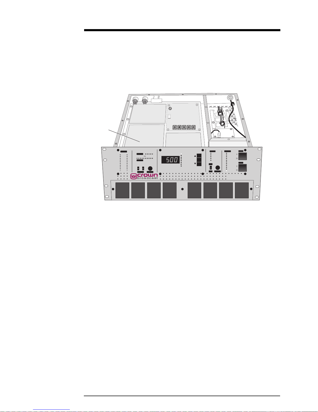
4.2 Audio Processor Circuit Board
The audio processor board provides the audio control functions of a compressor,
limiter, and expander. Illustration 6–5 and accompanying schematic may be useful
to you during this discussion.
Audio Processor
Carrier
Modulation
Audio Input
10
High
-6
-12
-18
Low
2
+6 dB
Wide Band
Expand
Compress
20
+12 dB
ProcessingInput Gain
®
2
High Band
RF Power
SWR
ALC
PA DC Volts
PA DC Amps
PA Temperature
Supply DC Volts
Voltmeter
Fault
SWR
Lock
Input
PA DC
PA Temp
Stereo
Mono RF Output
Over
100
90
80
70
60
Power
50
40
30
20
Pilot
FM500
FM BROADCAST TRANSMITTER
Illustration 4–2 Audio Processor Board
This board also contains the pre-emphasis networks. Reference numbers are for the
left channel. Where there is a right-channel counterpart, references are in
parenthesis. One processor circuit, the eighth-order elliptical filter, is located on
the stereo generator board.
Audio input from the XLR connector on the rear panel of the transmitter goes to
differential-input amplifier, U1A (U2A).
Binary data on the +6 dB and +12 dB control lines sets the gain of inverting
amplifier U1B (U2B). Analog switch, U3, selects one of four feedback points in 6 dB
steps.
The output of U1B (U2B) goes to an eighth-order, elliptical, switched-capacitor,
low-pass, 15.2 kHz filter. The filter finds its home on the stereo generator board to
take advantage of the ground plane and proximity to the 1.52 MHz clock.
The circuit associated with U4B (U4A), along with R22/C8 (R58/C20), form
third-order, low-pass filtering, attenuating audio products below 30 Hz.
The output level of analog multiplier U5 (U6) is the product of the audio signal at
pin 13 and the DC voltage difference between pins 7 and 9. At full gain (no gain
reduction) this difference will be 10 volts DC.
Principles of Operation
4–3
Page 42

m
o
t
o
s
n
n
d
e
e
u
q
o
s
n
i
u
n
,
i
e
s
r
o
m
c
h
a
o
i
f
c
i
d
e
n
e
d
v
o
i
s
r
c
s
a
m
o
t
o
s
m
e
u
q
o
s
n
i
u
n
,
i
e
s
r
o
m
c
h
a
o
i
f
c
i
d
e
n
e
d
v
o
i
s
r
c
s
a
m
n
e
d
v
i
r
c
s
a
m
o
t
o
s
m
e
u
q
o
s
n
i
u
n
,
i
e
s
r
o
m
c
a
o
i
f
c
i
d
e
n
e
d
v
i
s
r
c
s
a
m
d
v
o
i
r
o
d
i
c
e
e
c
o
n
d
o
d
i
c
e
e
c
o
o
c
o
n
d
d
i
c
h
e
o
c
o
c
c
o
s
,
n
,
n
n
o
,
e
n
n
a
m
o
t
o
s
n
m
d
e
o
u
,
q
o
s
n
i
u
d
,
i
in
c
e
e
s
r
o
f
o
m
c
h
a
e
ci
i
d
e
n
e
d
v
o
i
s
r
c
c
o
s
n
a
o
m
c
h
a
m
i
e
c
i
d
e
n
e
d
v
o
i
s
r
c
c
o
s
n
a
m
When either the positive or negative peaks of the output of U5 (U6) exceeds the
gain-reduction threshold, U13A generates DC bias, producing broadband gain
reduction. Q5 is a precision-matched transistor pair. Q5 and U13B form a log
converter, so that a given voltage change produces a given change in gain control
dB of U5 (U6). The log conversion ensures uniform level-processing characteristics
well beyond the 20 dB control range. The log conversion has an additional benefit;
it allows a display of gain control on a linear scale with even distribution of dB.
Q1 (Q2) is a recover/expansion gate with a threshold about 18 dB below the normal
program level. The amount of short-term expansion and gain reduction is
controlled by R650, located on the front panel display board. (See section 3.5.)
Pre-emphasis, in microseconds, is the product of the capacitance of C10 (C22),
multiplied by the gain of U8 (U9), times the value of R31 (R67). For a 75 µsecond
pre-emphasis, the gain of U8 (U9) will be about 1.11. Select the pre-emphasis curve
(75 µsec, 50 µsec, 25 µsec, or Flat) by jumpering the appropriate pins on header
JP1. Use trim pot R29 (R65) to make fine adjustments to the pre-emphasis. (See
section 5.1.)
For highband processing, the peak output of U10B is detected and gain-reduction
bias is generated, as with the broadband processor. The highband processing,
however, shifts the pre-emphasis curve rather than affecting overall gain.
Peak audio voltages are compared to a plus and minus 5 volt reference, U17 and
U18. This same reference voltage is used by the stereo generator, metering, and
display boards.
For an explanation of on-board adjustments see section 5.1.
4.3 Stereo Generator Circuit Board
The stereo generator board (see Illustration 4–3) generates a composite stereo signal
from left and right-channel audio inputs. The component side of the board is
mostly a ground plane. Once again, the eighth-order, 15.2 kHz, elliptical, low-pass
filters (U201 and U202) are on this board, but belong to the audio processor.
Illustration 6–6 and accompanying schematic complement this discussion.
U207A and Y201 comprise a 7.6 MHz crystal oscillator from which the 19 kHz and
38 kHz subcarriers are digitally synthesized. U207F is a buffer. The 7.6 MHz is
divided by 5 in U208A to provide 1.52 MHz at pin 6, used by filters U201 and U202.
3.8 MHz, 1.9 MHz, and 304 kHz are also derived from dividers in U208.
Exclusive-OR gates, U210A and U210B, provide a stepped approximation of a 38 kHz
sine wave—a scheme described in the
W. Sams &. Co., Inc., Indianapolis, IN, 1978).
With the resistor ratios used, the synthesized sine wave has very little harmonic
energy below the 7th harmonic. U210C and D generate the 19 kHz pilot subcarrier.
U211 is a dual, switched-capacitor filter, configured as second-order, low-pass filters,
4–4
CMOS Cookbook by Don Lancaster (Howard
FM500 User's Manual
Page 43
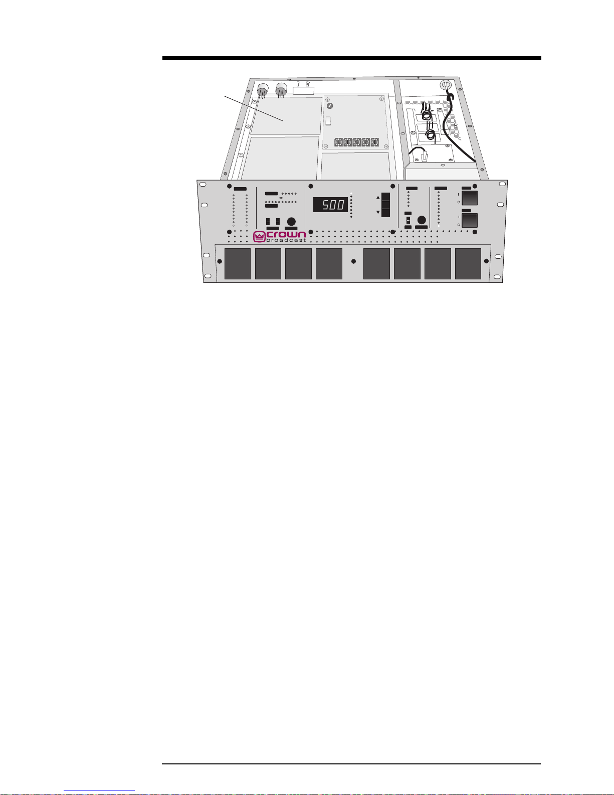
Stereo Generator
Audio Input
10
High
-6
-12
-18
Low
2
+6 dB
Wide Band
Expand
Compress
20
+12 dB
ProcessingInput Gain
®
2
High Band
RF Power
SWR
ALC
PA DC Volts
PA DC Amps
PA Temperature
Supply DC Volts
Voltmeter
Fault
SWR
Lock
Input
PA DC
PA Temp
Stereo
Mono RF Output
Over
100
90
80
70
60
Power
50
40
30
20
Pilot
FM500
FM BROADCAST TRANSMITTER
Carrier
Modulation
Illustration 4–3 Stereo Generator Board
each with a Q of 5. The 38 kHz and 19 kHz outputs of pins 1 and 20, respectively,
are fairly pure sine waves. Harmonic distortion products are better than 66 dB
down—THD of less than 0.05%.
U212 is a precision, four-quadrant, analog multiplier. The output of U212 is the
product of 38 kHz applied to the “X” input and the difference of left and right
audio (L-R signal) applied to the “Y” input. The resulting output is a double
sideband, suppressed carrier—the L-R subcarrier.
The SCA subcarrier, the left, right, and left-minus-right subcarriers, and the 19
kHz pilot subcarrier are combined into the composite stereo signal by summing
amplifier U206B.
Analog switch U205, at the input of U206B, provides switching of left and right
audio for stereo and mono modes. In the mono mode, right channel audio is
disabled, and the left channel audio is increased from 45% modulation to 100%.
MON L and MON R outputs go to the AF Monitor jacks on the rear panel.
R208+R210 (R220+R222) and C207 (C211) comprise a 75 µsec de-emphasis
network. Processed, de-emphasized (75 µsec) samples of the stereo generator
input signals are used for a studio monitor and for audio testing. Option jumpers
JP203 (JP204) allow you to select 50 µsec.
VR201 and VR202 supply +6 volts and –6 volts, respectively. A 5 volt reference
from the audio processor board supplies the subcarrier generators.
For an explanation of on-board adjustments see section 5.2.
Principles of Operation
4–5
Page 44
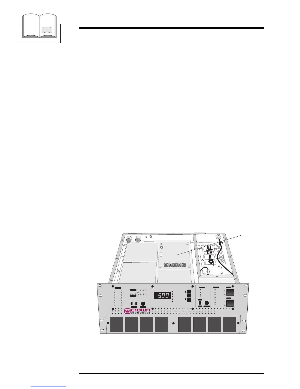
m
o
t
o
s
n
n
d
e
e
u
q
o
s
n
i
u
n
,
i
e
s
r
o
m
c
h
a
o
i
f
c
i
d
e
n
e
d
v
o
i
s
r
c
s
a
m
o
t
o
s
m
e
u
q
o
s
n
i
u
n
,
i
e
s
r
o
m
c
h
a
o
i
f
c
i
d
e
n
e
d
v
o
i
s
r
c
s
a
m
n
e
d
v
i
r
c
s
a
m
o
t
o
s
m
e
u
q
o
s
n
i
u
n
,
i
e
s
r
o
m
c
a
o
i
f
c
i
d
e
n
e
d
v
i
s
r
c
s
a
m
d
v
o
i
r
o
d
i
c
e
e
c
o
n
d
o
d
i
c
e
e
c
o
o
c
o
n
d
d
i
c
h
e
o
c
o
c
c
o
s
,
n
,
n
n
o
,
e
n
n
a
m
o
t
o
s
n
m
d
e
o
u
,
q
o
s
n
i
u
d
,
i
in
c
e
e
s
r
o
f
o
m
c
h
a
e
ci
i
d
e
n
e
d
v
o
i
s
r
c
c
o
s
n
a
o
m
c
h
a
m
i
e
c
i
d
e
n
e
d
v
o
i
s
r
c
c
o
s
n
a
m
4.4 RF Exciter Circuit Board
This board is also known as the Frequency Synthesizer board. The entire
component side of the board is a ground plane. Rotary switches along the front
edge of the board establish the operating frequency. The VCO (voltage-controlled
oscillator) circuitry is inside a shielded cover.
Illustration 6–7 and accompanying schematic can be used as reference in this
discussion. The following theory may apply to previous versions of the exciter
board, but it is typical of the operation of the current board which has the latest
technological improvements.
VCO, VCO61, operates at the synthesizer output frequency of 87 MHz to 108 MHz.
The frequency is controlled by voltage-variable capacitors DV71 and DV72. U7A
and U7B form an active filter to supply clean DC to the drain of Q71. They also
serve as a common-base RF amplifier for Q71. A71 and A1 are hybrid RF amplifiers
to provide buffering and gain.
A sample of the RF from the VCO goes to the input of A2. A2 amplifies the signal
and feeds it back to the synthesizer IC, U6. This signal, available at pin 4 of U6,
may be used with a high frequency receiver for deviation and frequency
measurements. (See sections 5.2 and 5.3.)
U6 is a phase-locked-loop frequency synthesizer IC. The 10.24 MHz from the
crystal oscillator is used by U6, along with ICs U1 through U3 and the frequency
selector switches, to generate the frequencies of the transmitter.
RF Exciter
Carrier
Modulation
Audio Input
10
High
-6
-12
-18
Low
2
+6 dB
Wide Band
Expand
Compress
20
+12 dB
ProcessingInput Gain
®
2
High Band
RF Power
SWR
ALC
PA DC Volts
PA DC Amps
PA Temperature
Supply DC Volts
Voltmeter
Fault
SWR
Lock
Input
PA DC
PA Temp
Stereo
Mono RF Output
Over
100
90
80
70
60
Power
50
40
30
20
Pilot
FM500
FM BROADCAST TRANSMITTER
4–6
Illustration 4–4 RF Exciter Board
FM500 User's Manual
Page 45

U6 is programmed with the four or five rotary switches. The binary output of the
0.1 MHz switch programs the “A” counter directly. BCD data from the 100’s, tens,
and units rotary switches is converted to binary data by U3 to set the “N” counter.
An optional fifth digit rotary switch for 10kHz spacing is available.
U5C is a differential amplifier and filter for the error signal. Audio that is out of
phase with that appearing on the error voltage is introduced by U5A, allowing for
greater loop bandwidth with less degradation of the low-frequency audio response.
U5D is an integrator. U5B is a VCO input voltage clamp.
DV71 and DV72 are hyper-abrupt varactor tuning diodes with a square-law
capacitance vs DC voltage curve, giving a straight-line frequency vs voltage curve
in a LC oscillator where the varactors are the dominant source of capacitance.
Lock and unlock status signals are available at the outputs of U4E and U4F,
respectively. Modulation is introduced to the VCO through R17 and R71 to R75.
About 4.1 millivolts across R75 produces 75 kHz deviation.
An FSK signal (used for automatic identification of FM repeaters) shifts the
frequencies of the 10.24 MHz crystal reference and the VCO. With keying, diodes
D9 and D10, are reverse biased, increasing the crystal reference frequency. At the
same time, current through R72 increases the VCO frequency. See section 5.3.4.
Principles of Operation
4–7
Page 46
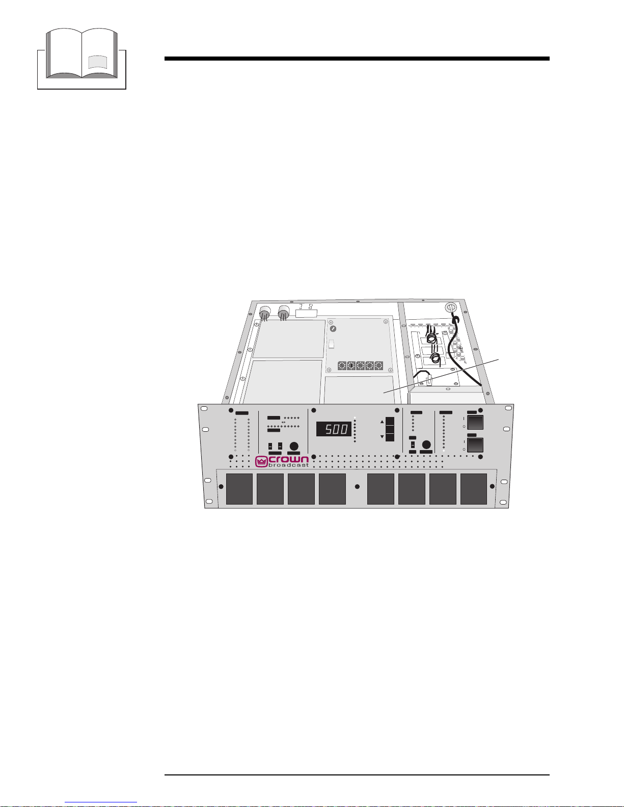
m
o
t
o
s
n
n
d
e
e
u
q
o
s
n
i
u
n
,
i
e
s
r
o
m
c
h
a
o
i
f
c
i
d
e
n
e
d
v
o
i
s
r
c
s
a
m
o
t
o
s
m
e
u
q
o
s
n
i
u
n
,
i
e
s
r
o
m
c
h
a
o
i
f
c
i
d
e
n
e
d
v
o
i
s
r
c
s
a
m
n
e
d
v
i
r
c
s
a
m
o
t
o
s
m
e
u
q
o
s
n
i
u
n
,
i
e
s
r
o
m
c
a
o
i
f
c
i
d
e
n
e
d
v
i
s
r
c
s
a
m
d
v
o
i
r
o
d
i
c
e
e
c
o
n
d
o
d
i
c
e
e
c
o
o
c
o
n
d
d
i
c
h
e
o
c
o
c
c
o
s
,
n
,
n
n
o
,
e
n
n
a
m
o
t
o
s
n
m
d
e
o
u
,
q
o
s
n
i
u
d
,
i
in
c
e
e
s
r
o
f
o
m
c
h
a
e
ci
i
d
e
n
e
d
v
o
i
s
r
c
c
o
s
n
a
o
m
c
h
a
m
i
e
c
i
d
e
n
e
d
v
o
i
s
r
c
c
o
s
n
a
m
4.5 Metering Circuit Board
The ALC and metering circuitry is on the metering board (see Illustration 4–4).
This board processes information for the RF and DC metering, and produces ALC
(RF level-control) bias. It also provides reference and input voltages for the digital
panel meter, voltages for remote metering, fan control, and drive for the
front-panel fault indicators.
Illustration 6–8 and accompanying schematic complement this discussion.
PA voltage and current come from a metering shunt on the power regulator board.
The PAI input is a current proportional to PA current; R405 converts the current
to voltage used for metering and control. A voltage divider from the PAV line is
used for DC voltage metering.
Metering
Audio Input
10
High
-6
-12
-18
Low
2
+6 dB
Wide Band
Expand
Compress
20
+12 dB
ProcessingInput Gain
®
2
High Band
RF Power
SWR
ALC
PA DC Volts
PA DC Amps
PA Temperature
Supply DC Volts
Voltmeter
Fault
SWR
Lock
Input
PA DC
PA Temp
Stereo
Mono RF Output
Over
100
90
80
70
60
Power
50
40
30
20
Pilot
FM500
FM BROADCAST TRANSMITTER
Carrier
Modulation
Illustration 4–5 Metering Board
U406A, U406B, and U407A, with their respective diodes, are diode linearity
correction circuits. Their DC inputs come from diode detectors in the RF
reflectometer in the RF low-pass filter compartment.
U407B, U407C, Q405, and Q406 are components of a DC squaring circuit. Since
the DC output voltage of U407C is proportional to RF voltage squared, it is also
proportional to RF power.
U404C, U404A, U403A, and U404D are level sensors for RF power, reflected RF
power, PA temperature, and external PA current, respectively. When either of
these parameters exceeds the limits, the output of U404B will be forced low,
reducing the ALC (RF level control) voltage, which, in turn, reduces the PA supply
voltage.
4–8
FM500 User's Manual
Page 47
The DC voltage setpoint for U404A (reflected RF voltage) is one-fifth that of U404C
(forward RF voltage). This ratio corresponds to an SWR of 1.5:1 [(1+.2)/(1–.2)=1.5].
The U405 inverters drive the front panel fault indicators.
To get a direct reading of SWR, the reference input of the digital panel meter is fed
from a voltage proportional to the forward-minus-reflected RF voltage, while
forward-plus-reflected is fed to the digital panel meter input. The panel meter
provides the divide function.
U408 & U409 function as data selectors for digital panel meter input and reference
voltages. Binary select data for U408 & U409 comes from the display board.
The output voltage of U403D goes positive when the temperature exceeds about 35
degrees C (set by R426) providing proportional fan control.
When the Carrier switch is off or the RF power is less than about 5 watts, the SWR
automatically switches to a calibrate-check mode. U406C provides a voltage that
simulates forward power, while Q403 shunts any residual DC from the reflectedpower source. The result is a simulation of a 1.0 to 1 SWR. (See section 5.4.)
4.6 Motherboard
The motherboard is the large board in the upper chassis interconnecting the audio
processor, stereo generator, RF exciter, and metering boards. The motherboard
eliminates the need for a wiring harness, and provides input/output filtering, test
points, and modular customization.
Motherboard components are passive with the exception of the fan driver transistor,
power FET Q501.
With Normal-Bypass slide switch SW501, it is possible to bypass the audio
processor, connecting the left and right audio inputs directly to the inputs of the
stereo generator.
CAUTION
In the BYPASS position, the pre-emphasis circuits and the filters that protect the
pilot and stereo subcarrier are bypassed. As a result, the occupied bandwidth
specifications of the transmitter could be compromised. The 15–Hz high-pass
filters are also bypassed which may mean that modulation with frequencies
below 10 Hz could cause the frequency synthesizer to unlock.
If the audio source is already processed, and further processing is not desired, use
the Normal mode instead of Bypass and turn the Processing control on the front
panel to “0”.
If it is necessary to provide resistive terminations at the audio inputs (either lineto-line or line-to-ground), you may place resistors directly into the 8–pin DIP
socket, A501, located between the XLR input connectors. See Illustration 6–9 and
accompanying schematic for the socket pin-out.
Principles of Operation
4–9
Page 48

m
o
t
o
s
n
n
d
e
e
u
q
o
s
n
i
u
n
,
i
e
s
r
o
m
c
h
a
o
i
f
c
i
d
e
n
e
d
v
o
i
s
r
c
s
a
m
o
t
o
s
m
e
u
q
o
s
n
i
u
n
,
i
e
s
r
o
m
c
h
a
o
i
f
c
i
d
e
n
e
d
v
o
i
s
r
c
s
a
m
n
e
d
v
i
r
c
s
a
m
o
t
o
s
m
e
u
q
o
s
n
i
u
n
,
i
e
s
r
o
m
c
a
o
i
f
c
i
d
e
n
e
d
v
i
s
r
c
s
a
m
d
v
o
i
r
o
d
i
c
e
e
c
o
n
d
o
d
i
c
e
e
c
o
o
c
o
n
d
d
i
c
h
e
o
c
o
c
c
o
s
,
n
,
n
n
o
,
e
n
n
a
m
o
t
o
s
n
m
d
e
o
u
,
q
o
s
n
i
u
d
,
i
in
c
e
e
s
r
o
f
o
m
c
h
a
e
ci
i
d
e
n
e
d
v
o
i
s
r
c
c
o
s
n
a
o
m
c
h
a
m
i
e
c
i
d
e
n
e
d
v
o
i
s
r
c
c
o
s
n
a
m
4.7 Display Circuit Board
The front-panel LEDs, the numeric display, the slide switches, and the processing
and RF level controls are mounted on the display circuit board. To access the
component side of the board, remove the front panel by removing 12 screws. The
board contains circuits for the digital panel meter, modulation peak detector, and
LED display drivers, as well as indicators and switches mentioned above.
Illustration 6–10 and accompanying schematic complement this discussion.
Left and right audio from input stages of the audio processor board (just after the
Input Gain attenuator) go to the L VU and R VU input on the display board. Peak
rectifiers U601A and U601B drive the left and right Audio Input displays. The LED
driver gives a 3 dB per step display. The lowest step of the display driver is not
used; rather a red LOW indicator lights when audio is below the level of the second
step. Transistors Q601 and Q602 divert current from the LOW LEDs when any
other LED of the display is lit.
Resolution of the linear displays, High Band, Wide Band, and Modulation, has been
improved using dither enhancement. With dither, the brightness of the LED is
controlled by proximity of the input voltage relative to its voltage threshold. The
effect is a smooth transition from step to step as input voltage is changed. U606A,
U606B, and associated components comprise the dither generator. Dither output
is a triangular wave.
Composite stereo (or mono) is full-wave detected by diodes D605 and D606. U607,
U613, Q603, and Q604 are components of a peak sample-and-hold circuit.
Oscillator, U609F, supplies a low-frequency square wave to the Fault indicators,
causing them to flash on and off.
Digital multimeter inputs are selected with push buttons located to the right of
the multimeter menu. Signals from the push buttons are conditioned by U609A
and U609B. U610 is an up/down counter. Binary input to U611 from U610 selects
a green menu indicator light, and lights the appropriate decimal point on the
numeric readout. The binary lines also go to analog data selectors on the ALC/
metering board.
Processing control, R650, is part of the audio processor. (See section 4.2.)
The DPM IN and DPM REF lines are analog and reference voltage inputs to digital
multimeter IC U612. They originate from analog data selectors on the ALC/
metering board.
4–10
FM500 User's Manual
Page 49

4.8 Voltage Regulator Circuit Board
The voltage regulator board is the longer of two boards mounted under the chassis
toward the front of the unit. It has switch-mode voltage regulators to provide +12,
–12, and 24 volts. It also contains the program detection and automatic carrier
control circuits.
Illustration 6–11 and accompanying schematic complement this discussion.
U703E and U703F convert a 38 kHz sine wave from the stereo generator into a
synchronization pulse. In the transmitter, synchronization is not used, thus D709
is omitted.
U704 and U705 form a 24 volt switching regulator running at about 35 kHz. U704
is used as a pulse-width modulator; U705 is a high-side driver for MOSFET switch
Q701. Supply voltage for the two IC’s (approximately 15.5 volts) comes from linear
regulator DZ702/Q705. Bootstrap voltage, provided by D710 and C714, allows the
gate voltage of Q701 to swing about 15 volts above the source when Q701 is turned
on. Current through the FET is sensed by R738 and R738A. If the voltage
between pin 5 and 6 of U705 exceeds 0.23 volts on a current fault, drive to Q701 is
turned off. Turn-off happens cycle by cycle. The speed of the turn-off is set by
C713.
U706 is a switching regulator for both +12 volts and –12 volts. It runs at about 52
kHz. Energy for –12 volts is taken from inductor L702 during the off portion of
the switching cycle. The –12 volts tracks the +12 volts within a few tenths of a
volt. There will be no –12 volts until current is drawn from the +12 volts.
Q702, Q703, and Q704 form an active filter and switch, supplying DC voltage to
the RF driver, when the Carrier switch is on.
The program detection circuit is made up of U701 and U702. U701A and U701D
and associated circuitry discriminate between normal program material and white
noise (such as might be present from a studio-transmitter link during program
failure) or silence. U701A and surrounding components form a band-pass filter
with a Q of 3 tuned to about 5 kHz. U701D is a first-order low-pass filter. Red and
green LEDs on the board indicate the presence or absence of program determined
by the balance of the detected signals from the two filters. U702 and U701C form a
count-down timer. The time between a program fault and shutdown is selected by
jumpering pins on header JP701. For times, see section 5.7. The times are
proportional to the value of R721 (that is, times can be doubled by doubling the
value of R721).
Principles of Operation
4–11
Page 50

m
o
t
o
s
n
n
d
e
e
u
q
o
s
n
i
u
n
,
i
e
s
r
o
m
c
h
a
o
i
f
c
i
d
e
n
e
d
v
o
i
s
r
c
s
a
m
o
t
o
s
m
e
u
q
o
s
n
i
u
n
,
i
e
s
r
o
m
c
h
a
o
i
f
c
i
d
e
n
e
d
v
o
i
s
r
c
s
a
m
n
e
d
v
i
r
c
s
a
m
o
t
o
s
m
e
u
q
o
s
n
i
u
n
,
i
e
s
r
o
m
c
a
o
i
f
c
i
d
e
n
e
d
v
i
s
r
c
s
a
m
d
v
o
i
r
o
d
i
c
e
e
c
o
n
d
o
d
i
c
e
e
c
o
o
c
o
n
d
d
i
c
h
e
o
c
o
c
c
o
s
,
n
,
n
n
o
,
e
n
n
a
m
o
t
o
s
n
m
d
e
o
u
,
q
o
s
n
i
u
d
,
i
in
c
e
e
s
r
o
f
o
m
c
h
a
e
ci
i
d
e
n
e
d
v
o
i
s
r
c
c
o
s
n
a
o
m
c
h
a
m
i
e
c
i
d
e
n
e
d
v
o
i
s
r
c
c
o
s
n
a
m
4.9 Power Regulator Circuit Boards
The power regulator boards are the two boards mounted under the chassis on
either side of a pair of 15,000 µf filter capacitors toward the front of the unit. Each
board has the switch-mode voltage regulator for a RF power amplifier, and
circuitry for PA supply current metering.
Illustration 6–12 and accompanying schematic complement this discussion.
Diode D804, in series with the battery input, together with the AC-supply diode
bridge, provides diode OR-ing of the AC and DC supplies.
U801 and U802 form a switching regulator running at about 35 kHz. U801 is used
as a pulse-width modulator; U802 is a high-side driver for MOSFET switch Q801.
Power for the two IC’s comes from the 24 volt supply voltage for the RF driver
(available when the Carrier switch is on). The voltage is controlled at 16 volts by
zener diode DZ801. Bootstrap voltage provided by D802 and C809 allows the gate
voltage of Q801 to swing about 16 volts above the source when Q801 is turned on.
Current through the FET is sensed by R812 and R812A. If the voltage from pin 5
to 6 of U802 exceeds 0.23 volts on a current fault, drive to Q801 is turned off. This
happens on a cycle-by-cycle basis. The speed of the turnoff is set by C805.
In the transmitter, synchronization is not used, thus D801 is omitted.
U803 and Q802 are used in a circuit to convert the current that flows through
metering shunt, R819, into a current source at the collector of Q803. Forty
millivolts is developed across R819 for each amp of supply current (.04 ohms x 1
amp). Q803 is biased by U803 to produce the same voltage across R816. The
collector current of Q803 is the same (minus base current) as that flowing through
R822 resulting in 40 microamperes per amp of shunt current. R405 on the
metering board converts Q803 collector current to 0.1 volt per amp of shunt
current (.04 ma X 2.49 k). (See section 5.4.)
4.10 RF Driver
The RF Driver module is mounted next to the heat sinks on the bottom of the RF
Amplifier/Combiner sub chassis. The driver amplifies the approximate 20
milliwatts from the frequency synthesizer to about 15 watts to drive the RF power
amplifiers. A CA2832 hybrid, high-gain, wideband amplifier, operating at about 20
volts, provides about one watt of drive to a single MRF137 MOSFET amplifier. The
MRF137 stage operates from a supply voltage of approximately 15 to 16 volts.
The circuit board has components for input and output coupling and for power
supply filtering.
4–12
FM500 User's Manual
Page 51
4.11 RF Amplifier
The two RF power amplifier modules are mounted on a combiner board, heat sink,
slide rail assembly which slides into the main chassis at the rear, and is fastened to
the back panel with six screws. RF power, DC power, and control voltages enter the
PA assembly through a 72–pin edge connector that it slides into at the front of the
chassis.
The amplifier is built around two Phillips BLF278, dual-power MOSFETs rated for
50 volts DC and a maximum power of about 300 watts. When biased for class B, the
transistor has a power gain of 20 dB. (It is biased below class B in the transmitter.)
Input transformer, T1111, is made up of two printed circuit boards. The four-turn
primary board is separated from the one-turn secondary by a thin dielectric film.
R1112–R1117 are for damping. Trim pot R1111 sets the bias.
Output transformer, T1121, has a one-turn primary on top of the circuit board and a
two-turn secondary underneath. Inductors L1121 and L1122 provide power line
filtering.
The amplifiers are surrounded by a 50 Ω impedance, input/output combiner board
which takes the 15 watts input and divides it equally to each power amp. Then the
output from each amplifier is combined to form a single output.
4.12 Chassis
The AC power supply components, as well as the bridge rectifier and main filter
capacitor are mounted on the chassis. Changing the jumpers on the AC
distribution board (located beside the transformer assembly on the bottom of the
transmitter), configures the power transformer for 100, 120, 220, or 240 VAC; see
section 2.2 for switching and fuse information. The board also includes MOV
voltage-surge suppressors and in-rush current limiters as well as a 12 volt power
supply for the PA assembly cooling fans.
The main energy-storage/filter capacitors are located between the two power
regulator boards. The DC voltage across each capacitor will be 65 to 70 volts when
the carrier is on.
WARNING
Shock hazard!
Do not attempt to short the capacitor
terminals. A bleeder resistor will
discharge the capacitor in
approximately one minute after
shutdown.
Principles of Operation
4–13
Page 52

m
o
t
o
s
n
n
d
e
e
u
q
o
s
n
i
u
n
,
i
e
s
r
o
m
c
h
a
o
i
f
c
i
d
e
n
e
d
v
o
i
s
r
c
s
a
m
o
t
o
s
m
e
u
q
o
s
n
i
u
n
,
i
e
s
r
o
m
c
h
a
o
i
f
c
i
d
e
n
e
d
v
o
i
s
r
c
s
a
m
n
e
d
v
i
r
c
s
a
m
o
t
o
s
m
e
u
q
o
s
n
i
u
n
,
i
e
s
r
o
m
c
a
o
i
f
c
i
d
e
n
e
d
v
i
s
r
c
s
a
m
d
v
o
i
r
o
d
i
c
e
e
c
o
n
d
o
d
i
c
e
e
c
o
o
c
o
n
d
d
i
c
h
e
o
c
o
c
c
o
s
,
n
,
n
n
o
,
e
n
n
a
m
o
t
o
s
n
m
d
e
o
u
,
q
o
s
n
i
u
d
,
i
in
c
e
e
s
r
o
f
o
m
c
h
a
e
ci
i
d
e
n
e
d
v
o
i
s
r
c
c
o
s
n
a
o
m
c
h
a
m
i
e
c
i
d
e
n
e
d
v
o
i
s
r
c
c
o
s
n
a
m
4.13 RF Output Filter & Reflectometer
The RF low-pass filter/reflectometer are located beside the motherboard in the
right-hand compartment on the top of the chassis. See Illustration 6–14 and
accompanying schematic for more information.
A ninth-order, elliptic, low-pass filter attenuates harmonics generated in the power
amplifier. The capacitors for the filter are circuit board pads.
The reflectometer uses printed circuit board traces for micro-strip transmission
lines. Transmission line segments (with an impedance of about 82 ohms) on
either side of a 50 ohm conductor provide sample voltages representative of the
square root of forward and reverse power.
DC voltages, representative of forward and reflected power, go through a bulkhead
filter board to the motherboard, then to the metering board, where they are
processed for power control, metering, and for SWR metering and protection.
4.15 Receiver Circuit Board Option
This option allows the transmitter to be used as a translator. The receiver board
receives terrestrially fed RF signal and converts it to composite audio which is then
fed into the exciter board. Microprocessor controlled phase lock loop technology
ensures the received frequency will not drift, and multiple IF stages ensure high
adjacent channel rejection. Refer to illustrations 4–6, 6–16 and its schematic for
the following discussion.
The square shaped metal can located on the left side of the receiver board is the
tuner module. The incoming RF signal enters through the BNC connector (top
left corner) and is tuned through the tuner module. Input attenuation is possible
with jumper J1 on the top left corner of the receiver board. Very strong signals
can be attenuated 20 dB automatically by placing the jumper on the left two pins
(“LO” position). An additional 20 dB attenuation is also available with the jumpers
in the top left corner of the board. The frequencies are tuned by setting switches
SW1 and SW2 (upper right corner). These two switches are read upon power up
by the microprocessor (U4). The microprocessor then tunes the synthesizer IC
SA1057 (U3) to the selected frequency. The switches frequency range is 87.9 Mhz
at setting “00” to 107.9 Mhz at setting “64”. Other custom ranges are available.
The synthesizer chip works on a phase lock loop system. It receives the frequency
information from pin 6 of the tuner module, then goes through a FET buffer
amplifier (Q2) on its way to synthesizer IC (U3). The synthesizer feeds back a DC
voltage through two resistors to pin 4 of the tuner module. Different frequencies
cause different tuning voltages to go to the tuner module to tune it on frequency.
The frequency synthesizer locks on to the exact frequency needed and adjusts the
DC voltage accordingly. The microprocessor tunes the frequencies of the
synthesizer IC, but the DC tuning voltage is somewhat dependent on the tuner
module.
4–14
FM500 User's Manual
Page 53
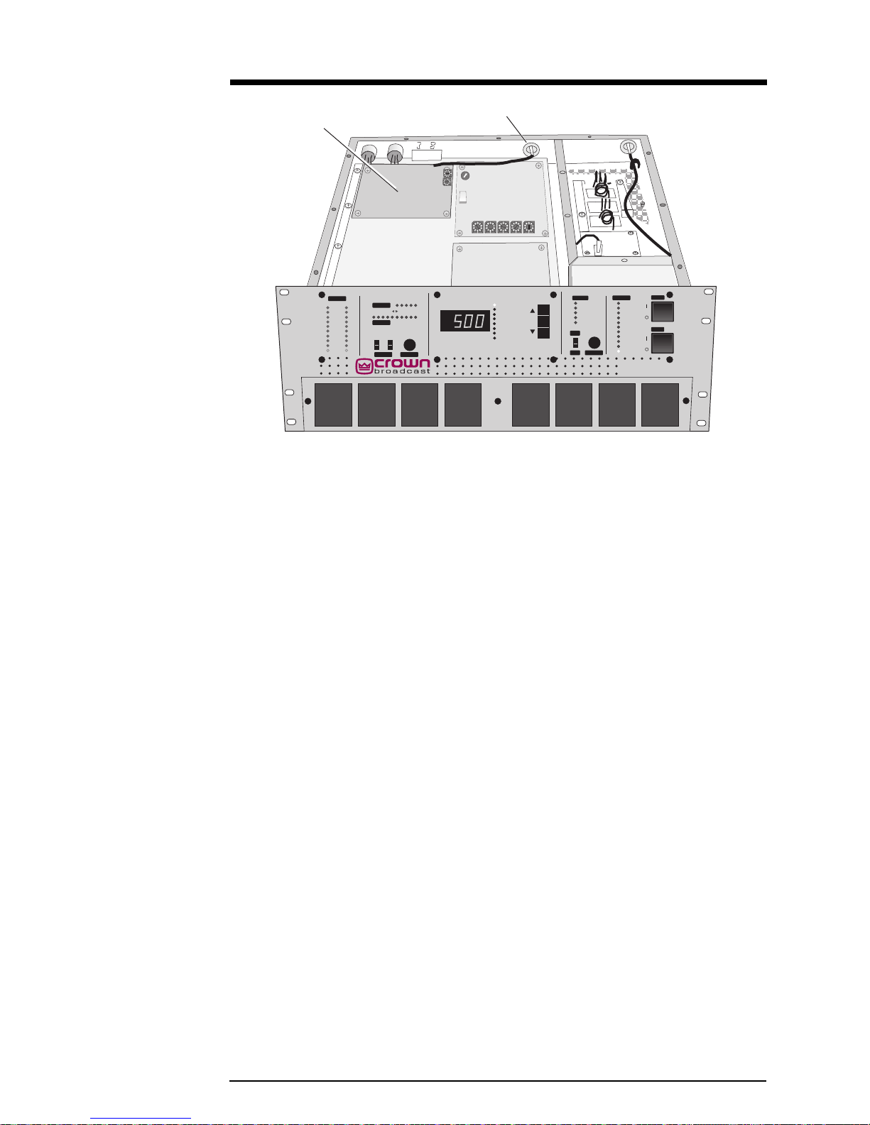
Receiver Module
(option)
Audio Input
High
-6
-12
-18
Low
Illustration 4–6 Receiver Board (optional)
Stereo
Generator
2
High Band
Expand
Compress
2
Wide Band
+12 dB
+6 dB
ProcessingInput Gain
RF IN
Carrier
Modulation
10
20
®
RF Power
SWR
ALC
PA DC Volts
PA DC Amps
PA Temperature
Supply DC Volts
Voltmeter
Fault
SWR
Lock
Input
PA DC
PA Temp
Stereo
Mono RF Output
Over
100
90
80
70
60
Power
50
40
30
20
Pilot
FM500
FM BROADCAST TRANSMITTER
Generally, the voltage is around 0.5 volt DC for tuning 88.1 MHz, and from 5.5 to
6.5 volts DC for tuning 107.9 MHz. The 10.7 MHz IF frequency comes out of the
tuner module on pin 5 and is coupled into the first filter FL1; passes through FL1
and into the IF decoder system of IC LM1865 (U1). The FL1 filter sets the
bandwidth or everything outside of the bandwidth depending on the filter that is
selected. It could be a bandwidth of 180 kHz where everything outside of that is
filtered out depending on the filter characteristics. A second filter (F3) is available
when the signal has a great amount of interference from an adjacent signal. In
such a case, remove the jumper cap that is in the F3 position, then remove the
ceramic filter that is in the F4 storage position and place it into the F3 position.
Then the signal goes to a buffer gain stage at pin 1 of LM1865 (U1). From there
the signal passes through F2, which is a second filter for further removal of
unwanted products, and then it goes on to the IF of that chip. The quadrature coil
L4 is tuned to 10.7 MHz as per calibration procedures. This results in a low
distortion of around 0.2 to 0.3% on the audio. The audio, still a composite at this
point, will come out of pin 15 of that IC (U1) and go to the first buffer U9. Then it
goes through a compensation network R54 and C26, and on to the stereo decoder
chip at pin 2 of U5.
When a stereo signal is present, Led 1 illuminates which indicates that left and
right audio is available. Then the stereo signals go to gain stages U6A and U6B and
out to the RCA jacks on the back of the cabinet. These can be used for off-air
monitoring of the audio signal. Incoming frequency can be monitored from the
frequency monitor BNC jack on the back. The stereo buffer U9, stereo decoder U5,
and gain stages U6A and U6B have no effect on the signal that goes through the
transmitter. This section along with the composite signal coming out of pin 15 of
LM1865 (U1) is totally separate from the transmitter section.
Principles of Operation
4–15
Page 54

m
o
t
o
s
n
n
d
e
e
u
q
o
s
n
i
u
n
,
i
e
s
r
o
m
c
h
a
o
i
f
c
i
d
e
n
e
d
v
o
i
s
r
c
s
a
m
o
t
o
s
m
e
u
q
o
s
n
i
u
n
,
i
e
s
r
o
m
c
h
a
o
i
f
c
i
d
e
n
e
d
v
o
i
s
r
c
s
a
m
n
e
d
v
i
r
c
s
a
m
o
t
o
s
m
e
u
q
o
s
n
i
u
n
,
i
e
s
r
o
m
c
a
o
i
f
c
i
d
e
n
e
d
v
i
s
r
c
s
a
m
d
v
o
i
r
o
d
i
c
e
e
c
o
n
d
o
d
i
c
e
e
c
o
o
c
o
n
d
d
i
c
h
e
o
c
o
c
c
o
s
,
n
,
n
n
o
,
e
n
n
a
m
o
t
o
s
n
m
d
e
o
u
,
q
o
s
n
i
u
d
,
i
in
c
e
e
s
r
o
f
o
m
c
h
a
e
ci
i
d
e
n
e
d
v
o
i
s
r
c
c
o
s
n
a
o
m
c
h
a
m
i
e
c
i
d
e
n
e
d
v
o
i
s
r
c
c
o
s
n
a
m
A muting circuit, consisting of C22, a 1N914 diode, R14, and varible resistor R15
mutes the output when a signal is too weak to be understood. The strength of the
signal muted is determined by the adjustment of R15. Any signal below the setting
of R15 is shorted to +VCC through C22 by the current drawn through R14 and the
diode. The audio signal above this setting goes through C17 to the connector P3.
The P3 connector block allows jumpering to either internal circuitry or to external
signal processing such as advertisement injection or other forms of altering the
signal. If the jumper is installed for internal circuitry, the signal will go through
R39 to the input of U2A. This is a buffer that drives the R20 pot located on the top
left hand corner of the board. R20 sets signal gain for 100% modulation if
adjusted correctly with a full incoming 75 kHz deviation signal. Then the signal
goes through R21, R22, and C20 which, along with adjustable pot R24 and C21,
forms a compensation network with some phase shifting. This allows the best
stereo separation possible by adjusting and compensating for differences in FM
exciter boards. The signal is buffered through U2B and finally reaches the output
connectors P1 and P2, and on to the transmit circuitry.
The power supply is fairly straight forward. The incoming 12 volt supply goes to a
7809, 9 volt regulator (VR1) which supplies all 9–volt needs on the board. The 9
volts also supplies a 7805, 5 volt regulator (VR2) which supplies all 5–volt needs on
the board. Plus and minus 12 volts from the motherboard is filtered and supplies
various needs on the board. Finally there is a precision reference voltage supplied
through R50 by U7 and U8. These two 2.5 volt reference shunts act very much like
a very accurate zenor diode to provide precision 5 volts to the metering board.
4–16
FM500 User's Manual
Page 55
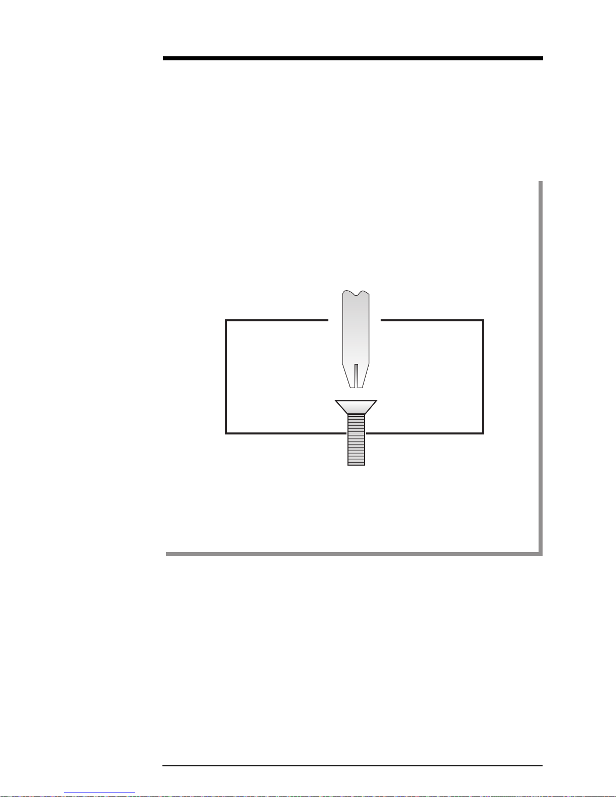
Section 5—Adjustments and Tests
This section describes procedures for (1) advanced users who may
be interested in customizing or optimizing the performance of
the transmitter and (2) service personnel who want to return the
transmitter to operational status following a maintenance procedure.
Adjustments and Tests
5–1
Page 56

5.1 Audio Processor Adjustments
5.1.1 Pre-Emphasis Selection
Select the pre-emphasis curve (75 µsec, 50 µsec, 25 µsec, or Flat) by jumpering the
appropriate pins of header JP1 on the audio processor board. (See section 2.9.) If
you change the pre-emphasis, change the de-emphasis jumpers, JP203 and JP204
on the Stereo Generator board, to match. (See section 2.8.)
5.1.2 Pre-Emphasis Fine Adjustment
T rim potentiometers, R29 and R65, (for left and right channels, respectively)
provide for fine adjustment of the pre-emphasis. Set the potentiometers to bring
the de-emphasized gain at 10 kHz equal to that of 400 Hz. (At the proper setting,
15.0 kHz will be down about 0.7 dB.)
When making these adjustments, it is important that you keep signal levels below
the processor gain-control threshold.
A preferred method is to use a precision de-emphasis network in front of the audio
input. Then, use the non-de-emphasized (flat) output from the FM modulation
monitor for measurements.
5–2
FM500 User's Manual
Page 57

5.2 Stereo Generator Adjustments
5.2.1 Separation
Feed a 400 Hz sine wave into one channel for at least 70% modulation. Observe the
classic single-channel composite stereo waveform at TP1 on the RF Exciter circuit
board. Adjust the Separation control for a straight centerline.
Since proper adjustment of this control coincides with best stereo separation, use
an FM monitor to make or confirm the adjustment.
5.2.2 Composite Output
Adjust the composite output with a modultion monitor following the steps below:
1. Set the Stereo-Mono switch to Mono.
2. Check that the setting of the Modulation compensation control, R17 on the
RF Exciter circuit board, falls within the range specified for the frequency of
operation. (See section 2.3.1.)
3. Feed a sine wave signal of about 2.5 kHz into the left channel at a level
sufficient to put the wideband gain-reduction indicator somewhere in the
middle of its range.
4. Set the Composite level control to produce 90% modulation as indicated on
an FM monitor.
5. Apply pink noise or program material to the audio inputs and confirm, on
both Mono and Stereo, that modulation peaks are between 95% and 100%.
5.2.3 19 kHz Level
Adjust the 19 kHz pilot for 9% modulation as indicated on an FM modulation
monitor . (The composite output should be set first, since it follows the 19 kHz
Level control.)
5.2.4 1 9 kHz Phase
1. Apply a 400 Hz audio signal to the left channel for at least 70% modulation.
2. Look at the composite stereo signal at TP301 on the RF Exciter circuit board
with an oscilloscope, expanding the display to view the 19 kHz component on
the horizontal centerline.
3. Switch the audio to the right-channel input. When the 19 kHz Phase is
properly adjusted, the amplitude of the 19 kHz will remain constant when
switching between left and right.
4. Recheck the separation adjustment as described in section 5.2.1.
Adjustments and Tests
5–3
Page 58

5.3 Frequency Synthesizer Adjustments
5.3.1 Frequency (Channel) Selection
Refer to section 2.3.
5.3.2 Modulation Compensator
Refer to section 2.3.
5.3.3 Frequency Measurement and Adjustment
Next to the 10.24–MHz crystal on the RF Exciter board is a 1–11 pF piston trimmer
capacitor (C3). Use C3 to set the frequency of the 10.24–MHz crystal while
observing the output frequency of the synthesizer .
Use one of these methods for checking frequency:
❑ Use an FM frequency monitor .
❑ Couple a frequency counter of known accuracy to the output of the synthesizer
and observe the operating frequency.
circuit.)
(Do not connect to the 10.24–MHz clock
5.3.4 FSK Balance Control
An FSK signal (used for automatic identification of FM repeaters) shifts the
frequencies of the 10.24–MHz crystal reference oscillator and the VCO.
Use an oscilloscope to observe the cathode end of D4. With no program, the pulse
will be less than 1 µsec wide. With an FSK input (a 20–Hz square wave at the FSK
input will work), set trim pot R45 for minimum pulse width.
The setting will vary slightly with operating frequency.
5–4
FM500 User's Manual
Page 59
5.4 Metering Board Adjustments
5.4.1 Power Calibrate
While looking at RF Power on the digital panel meter , set the Power Calibrate trim
potentiometer to agree with an external RF power meter .
5.4.2 Power Set
With the front panel RF Output control fully clockwise, adjust the Power Set trim
pot to 10% more than the rated power (33 W for FM30, 110 W for FM100, 275 W
for FM250, 550 W for FM500) as indicated on an accurate external watt meter. If
the authorized power is less than the maximum watts, you may use the Power Set
to limit the range of the RF Output control. Operation below 100 watts is not
recommended as instability can occur which could damage the transmitter .
CAUTION
Possible equipment damage!
Operation below 100 watts can cause
oscillations and other problems that
could damage the transmitter.
5.4.3 SWR Calibrate
When the Carrier switch is off, or the RF power is less than about 5 watts, the SWR
circuit automatically switches to a calibrate-check mode. (See section 4.5 for more
information.)
Set the digital panel meter to read SWR. With the Carrier switch off, set the SWR
CAL trim pot to read 1.03.
5.4.4 PA Current Limit
Since it may not be practical to increase the PA current to set the PA Current Limit
control, you may use this indirect method.
With the
Metering board. The current limit, in amperes, will be 0.35 amps higher than ten
times this voltage. Set the current limit for 16.5 amps or 1.615 volts at R413.
carrier turned off, look at the DC voltage at the right end of R413 on the
Adjustments and Tests
5–5
Page 60

5.5 Motherboard Adjustments
For Normal-Bypass switch setting, see section 2.10.
5.6 Display Modulation Calibration
The Modulation Calibrate trim pot sets the sensitivity of the front panel Modulation
bar graph display.
This adjustment may be made only after the Output trim pot on the Stereo
Generator board has been set. (See section 5.2.4.)
1. Set the Stereo-Mono switch to Mono.
2. Feed a sine wave source of about 2.5 kHz into the left channel at a level
sufficient to put the wideband gain-reduction indicator somewhere in the
middle of its range.
3. Set the Modulation Calibrate trim pot so that the “90” light on the front panel
Modulation display just begins to light.
5.7 Voltage Regulator Adjustments
JP701, a 10–pin header on the Voltage Regulator board, sets the time between
program failure and carrier turnoff. Pins 1 and 2 are the two pins closest to the
edge of the board. The times are approximate. Sections 2.11, 2.12, and 4.8
contain further information.
1. Short pins 1 and 2 for a 30–second delay.
2. Short pins 3 and 4 for a 2–minute delay.
3. Short pins 5 and 6 for a 4–minute delay.
4. Short pins 7 and 8 for an 8–minute delay.
You may select other times by changing the value of R721. The time is proportional
to the resistance.
5.8 Bias Set (RF Power Amplifier)
The Bias Set trim pot is located on the PA module on the input circuit board. Set
the trim pot to its midpoint for near-optimum bias.
5–6
FM500 User's Manual
Page 61

5.9 Performance Verification
Measure the following parameters to receive a comprehensive characterization of
transmitter performance:
❑ Carrier frequency
❑ RF output power
❑ RF bandwidth and RF harmonics (see section 5.12)
❑ Pilot frequency, phase, and modulation percentage
❑ Audio frequency response
❑ Audio distortion
❑ Modulation percentage
❑ FM and AM noise
❑ Stereo separation between left and right
❑ Crosstalk between main channel and subcarrier
❑ 38–kHz subcarrier suppression
In addition to the above tests, which pertain to signal quality, a complete check of
the unit will include items listed in section 5.21.
5.9.1 Audio Proof-of-Performance Measurements
References to “100%” modulation assume 9% pilot and 91% for the remainder of
the composite stereo signal.
Because the audio processing threshold is at 90% modulation, it is not possible to
make audio proof-of-performance measurements at 100% modulation through the
audio processor. Instead, audio data for 100% modulation is taken from the input
of the stereo generator (SW501 on Motherboard set for Bypass). Then, data,
including the audio processor (SW501 set for Normal), is taken at a level below the
audio processing threshold.
5.9.2 De-emphasis Input Network
A precision de-emphasis network, connected between the test oscillator and the
audio input of the transmitter, can be very helpful when making the audio
measurements. Note that the input impedance of the transmitter or the source
impedance of the test oscillator can affect network accuracy. With the de-emphasis
network, oscillator level adjustments need only accommodate gain errors, instead of
the whole pre-emphasis curve.
Adjustments and Tests
5–7
Page 62

5.10 Carrier Frequency
Carrier frequency is measured at the output frequency with a frequency monitor or
suitable frequency counter .
To adjust frequency, see section 5.3.3. (FCC tolerance +/– 2000 Hz per FCC Part
73.1540 and 73.1545.)
5.11 Output Power
The output power reading on the front panel display should be 90–105% of the
actual value. For a more precise measurement, use a watt meter in the RF output
line. See sections 5.4.1 and 5.4.2 for setting power.
5.12 RF Bandwidth and RF Harmonics
You can observe RF bandwidth and spurious emissions with an RF spectrum
analyzer .
In the Stereo mode, feed a 15.0 kHz audio signal into one channel to provide 85%
modulation as indicated on a monitor. Doing so produces 38% main, 38% stereo
subcarrier, and 9% pilot per FCC Part 2.989. As an alternative, use pink noise into
one channel.
Using a spectrum analyzer, verify the following (per FCC 73.317):
1. Emissions more than 600 kHz from the carrier are at least 43 + 10log(power,
in watts) dB down (70 dB for 500 watts). The scan should include the tenth
harmonic.
2. Emissions between 240 kHz and 600 kHz from the carrier are down at least
35 dB.
3. Emissions between 120 kHz and 240 kHz from the carrier are down at least
25 dB.
5.13 Pilot Frequency
The pilot frequency should be within 2 Hz of 19 kHz. (FCC Part 73.322.) Using a
frequency counter , measure 1.9 MHz at pin 1 of U209 on the Stereo Generator
board. A 200-Hz error here corresponds to a 2-Hz error at 19 kHz. If the frequency
is off by more than 50 Hz, you may change the value of C213. (Changing C213 from
56 pF to 68 pF lowers the 1.9 MHz by about 35 Hz.)
5–8
FM500 User's Manual
Page 63

5.14 Audio Frequency Response
For the response tests, take the readings from an FM modulation monitor .
Make audio frequency response measurements for left and right channels at
frequencies of 50 Hz, 100 Hz, 400 Hz, 1 kHz, 5 kHz, 10 kHz, and 15 kHz. See
sections 5.9.1 and 5.9.2.
5.15 Audio Distortion
Make distortion measurements from the de-emphasized output of an FM
modulation monitor .
Make audio distortion measurements for left and right channels at frequencies of 50
Hz, 100 Hz, 400 Hz, 1 kHz, 5 kHz, 10 kHz, and 15 kHz. See sections 5.9.1 and
5.9.2.
5.16 Modulation Percentage
While feeding an audio signal into the left channel only, confirm that the total
modulation percentage remains constant when switching between Mono and
Stereo.
Measure modulation percentage with an FM modulation monitor , or by using an HF
receiver and Bessel nulls. See section 5.2.2.
19–kHz pilot modulation should be 9%.
5.17 FM and AM Noise
T ake noise readings from a de-emphasized output of a modulation monitor.
5.18 Stereo Separation
Make left-into-right and right-into-left stereo separation measurements with an FM
modulation monitor for frequencies of 50 Hz, 100 Hz, 400 Hz, 1 kHz, 5 kHz, 10
kHz, and 15 kHz.
5.19 Crosstalk
For stereo crosstalk measurements, both left and right channels are fed at the same
time. For best results, there needs to be a means of correcting small imbalances in
levels and phase. The balance is made at 400 Hz.
Adjustments and Tests
5–9
Page 64

5.19.1 Main Channel Into Sub
Feed the left and right channels in phase with audio (L+R) at 50 Hz, 100 Hz, 400
Hz, 1 kHz, 5 kHz, 10 kHz, and 15 kHz at 100% modulation, while observing the
stereo subcarrier (L-R) level on an FM modulation monitor .
5.19.2 Sub Channel Into Main
Feed the audio into the left and right channel as above, with the exception of
reversing the polarity of the audio of one channel (L-R input). Using the
frequencies of 5.19.1 above, observe the main channel (L+R) level with a
modulation monitor .
5.20 38 kHz Subcarrier Suppression
With no modulation, but in the Stereo mode, the 38 kHz subcarrier , as indicated on
an FM modulation monitor, should be down at least 40 dB.
5.21 Additional Checks
In addition to the tests and adjustments mentioned in this section, the following
checks ensure a complete performance appraisal of the transmitter:
1. Perform a physical inspection, looking for visible damage and checking that
the chassis hardware and circuit boards are secure.
2. Check the functionality of switches and processing control.
3. Verify that all indicators function.
4. Check the frequency synthesizer lock at 80 MHz and 110 MHz.
5. Measure the AC line current with and without the carrier on.
6. Perform a functional test of the SCA input, Monitor outputs, and the monitor
and control function at the 15–pin, D-sub connector .
7. T est the functionality of the FSK circuit.
8. Check the operation and timing of the automatic carrier-off circuitry associated with program failure.
9. Check all metering functions.
10. Test ALC action with PA current overload, SWR, and PLL lock.
NOTE:
FCC type acceptance procedures call for testing the carrier frequency over the
temperature range of 0–50 degrees centigrade, and at line voltages from 85% to
115% of rating. (See FCC Part 2.995.)
5–10
FM500 User's Manual
Page 65
Section 6—Reference Drawings
The illustrations in this section may be useful for making adjustments, taking measurements, troubleshooting, or understanding
the circuitry of your transmitter.
Reference Drawings
6–1
Page 66
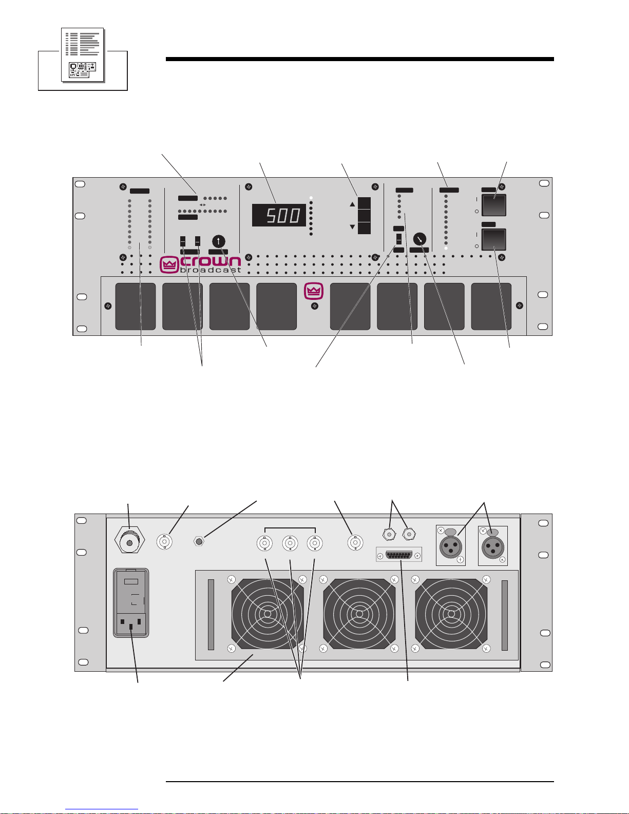
6.1 Views
Gain Reduction/Expansion
Indicators
Audio Input
High
-6
-12
-18
Low
High Band
2
Wide Band
+6 dB
Audio Processor
Input Level
Indicators
Input Gain
2
Expand
Compress
+12 dB
ProcessingInput Gain
Switches
10
20
®
RF Power
SWR
ALC
PA DC Volts
PA DC Amps
PA Temperature
Supply DC Volts
Voltmeter
Processing Control
Stereo/Mono Switch
Illustration 6–1 Front View
Modulation
Indicators
Fault
SWR
Lock
Input
PA DC
PA Temp
Stereo
Mono RF Output
Fault Indicators
Carrier SwitchDigital Multimeter Multimeter Select
Modulation
Over
100
90
80
70
60
50
40
30
20
Pilot
FM500
FM BROADCAST TRANSMITTER
Power Switch
Relative RF
Voltage Out
Carrier
Power
RF Output
FUSE
AC Power In
RF Output
Monitor
Power Amplifier
and Cooling
Ground
1
Composite
Input
SCA IN
23
COMPOSITE IN
SCA Inputs
Illustration 6–2 Rear View
MONITOR
R
REMOTE I/O
Remote I/O
Audio InputsAudio Monitors
RIGHT
L
LEFT/MONO
6–2
FM500 User's Manual
Page 67
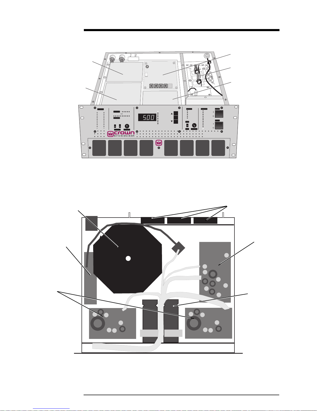
Stereo Generator
RF Exciter
Low-pass Filter
Audio Processor
Power Transformer
Audio Input
Metering
10
High
-6
-12
-18
Low
2
Wide Band
+6 dB
Expand
Compress
20
+12 dB
ProcessingInput Gain
®
2
High Band
RF Power
SWR
ALC
PA DC Volts
PA DC Amps
PA Temperature
Supply DC Volts
Voltmeter
Fault
SWR
Lock
Input
PA DC
PA Temp
Stereo
Mono RF Output
Over
100
90
80
70
60
Power
50
40
30
20
Pilot
FM500
FM BROADCAST TRANSMITTER
Carrier
Modulation
Illustration 6–3 Chassis Top View
Power Amp
Fans
Power
Distribution
Board
Power Regulator
Boards
Voltage Regulator
Board
Filter Capacitors
front of transmitter
Illustration 6–4 Chassis Bottom View
Reference Drawings
6–3
Page 68
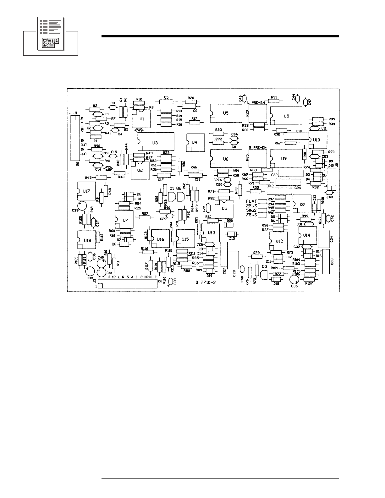
6.2 Board Layouts and Schematics
6–4
Illustration 6–5 Audio Processor Board
FM500 User's Manual
Page 69
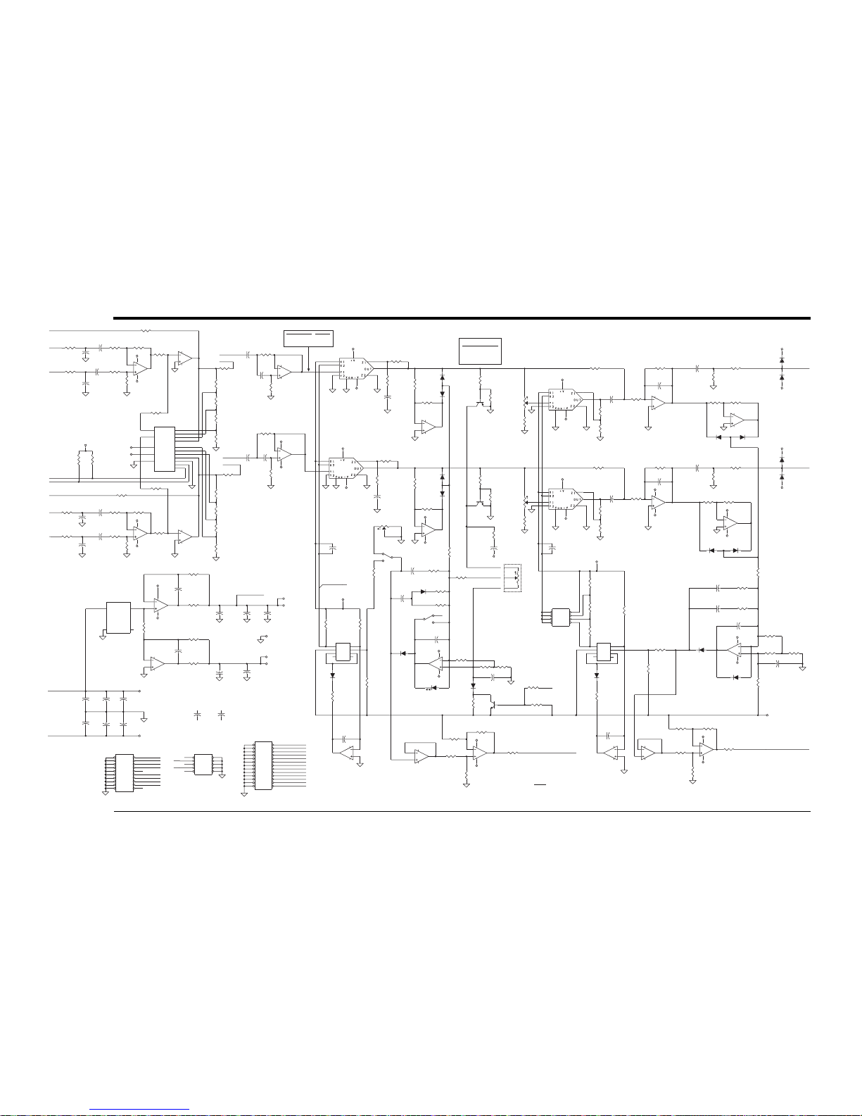
6–5
Reference Drawings
L OUT
+5V
-5V
D3
D4
FLAT A=0
75uSEC A=1.0
50uSEC A=0.67
25uSEC A=0.33
GAIN: U5, Pin 2 to U8, Pin 2
(No Hi-band gain reduction)
C11
220PF
R35
240K
+12V
C12
0.1
R26
100K
R38
1K
R31
24.9K
1
R34
24.9K 1
(+/-5.0V PK)
GAIN REDUCTION VOLTS P-P
THRESHOLD 1.1
10DB 3.5
20DB 11
D2
R17
360K
L LP2
L LP1
+12V
-12V
C6
.047
7
9
1
12
13
2
10
1
4
31
1
U5
AD632
R1
100
R22
11.3K
1
6
5
7
U4B
TL072
R24
24.9K
1
C5
.047
R20
75K
1
R13
2.0K
1
R23
100K 1
L VU
L IN1
L IN2
+12V
-12V
C3
1.0
C1
100PF
C2
100PF
R2
1K
R3
1K
R9
1K
R4
24.9K
1
R5
24.9K
1
R6
24.9K
1
C4
1.0
R7
24.9K
1
2
3
1
8
4
U1A
TL072
6
5
7
U1B
TL072
R8
30.1K
1
16
7
8
R44
24.9K
R42
24.9K
R43
24.9K
R45
24.9K
/+6DB
/+12DB
R VU
R IN1
R IN2
+5V
+12V
-12V
+5V
-5V
C16
1.0
C15
1.0
C13
100PF
C14
100PF
R40
1K
R41
1K
R48
1K
2
3
1
8
4
U2A
TL072
6
5
7
U2B
TL072
R12
20K 1
R49
20K 1
R47
30.1K
1
X0
12
X1
14
X2
15
X3
11
Y0
1
Y1
5
Y2
2
Y3
4
INH
6
A
10
B
9
X
13
Y
3
U3
74HC4052
R10
47K
R11
47K
(+/-5.0V PK)
R60
24.9K
2
3
1
8
4
U7A
TL072
R61
24.9K
C50
47PF
R LP2
R LP1
+12V
+12V
+12V
-12V
-12V
-12V
C8
1.0
POLY
C20
1.0
POLY
R59
100K 1
R58
11.3K
1
D1
D7
D8
2
3
1
8
4
U4A
TL072
R14
1.0K
1
R15
499
1
R98
100
R51
1.0K
1
R52
499
1
6
5
7
U7B
TL072
R25
24.9K
1
C17
.047
C18
.047
R46
360K
7
9
1
12
13
2
10
1
4
31
1
U6
AD632
R16
499
1
R53
499
1
R56
75K
1
R50
2.0K
1
R87
3.3K
2
1
3
SW1A
R123
50K
PRE-EMP.
PRE-EMP.
D6
D11 D12
R73
24.9K
6
5
7
U10B
TL072
R67
24.9K
R70
24.9K
R72
24.9K
R36
24.9K
R37
24.9K
D5
Q1
2N5087
R64
OPEN
R28
OPEN
C23
220PF
R71
240K
C49
47PF
+12V
+12V
+12V
-12V
-12V
-5V
-12V
-12V
C24
0.1
C29
0.1
C22
.0027
POLY
Q2
2N5087
R62
100K
R29
10K
R65
10K
R33
10K
R69
10K
R32
12K
7
9
1
12
13
2
10
1
4
31
1
U8
AD632
R68
12K
7
9
1
12
13
2
10
1
4
31
1
U9
AD632
2
3
1
8
4
U10A
TL072
R39
1K
R74
1K
R81
1K
R90
1K
2
3
1
8
4
U12A
TL072
6
5
7
U12B
TL072
R30
49.9K
1
R66
49.9K
1
C10
.0027
POLY
D10
D9
R OUT
+5V
-5V
R109
3.3K
-5V
C35
1.0
R107
10K
R106
1K
R105
1M
D18
560
LIGHT
3mV/DB
HEAVY
.25V/DB
E
B
C
R650
POT LOCATED
ON DISPLAY PCB
FLAT
25uS
50uS
75uS
D16
D17
R77
3.3K
100K
1
1
2
2
3
3
4
4
8
8
7
7
6
6
5
5
Q7
LM394
Q3
2N5210
PROC A
PROC B
PROC C
TEST
+5V
+12V
-12V
C33
.047
C34
OPEN
C30
1.0
C31
100PF
C32
100PF
R76
10K
R93
10K
R101
10K
R100
120
R92
1K
D15
2
3
1
8
4
U14A
TL072
R104
OPEN
R99
3.3K
D21
R75
2.4K
R94
20.0K
1
R95
20.0K
1
R96
20.0K
1
R97
49.9K
1
R112
49.9K
1
R115
49.9K
1
R116
49.9K
1
1 2
3 4
5 6
7 8
JP1
HEADER 4X2
R103
3.3K
3mV/DB
-5VDC at 0DB GR
4.1V at 20 DB GR
7
E
B
C
D19
R89
330K
D13
1
1
2
2
3
3
4
4
8
8
7
7
6
6
5
5
Q5
LM394
+5V
-5V
+5.00V
+5V
+12V
-12V
+5V
-5V
VDD
VSS
VEE
C46
0.1
C47
0.1
C48
0.1
C25
100PF
C26
100PF
R78
91K
R88
10M
R91
10M
R82
120
C28
1.0
POLY
2
3
1
8
4
U13A
TL072
C27
.047
R86
3.3M
D20
R80
3.3K
R111
49.9K
1
C38
1.0
C39
1.0
D14
YEL
R85
3.3K
R79
49.9K
1
R83
10K
5
4
6
SW1B
IN
2
GND
4
VO
6
TRM
5
U17
REF02
2
3
1
8
4
U18A
TL072
+12V
-12V
+12V
-12V
+12V
-12V
C36
.01
C37
.01
C42
0.1
C43
0.1
C45
0.1
C44
0.1
R121
10.0K 1
R122
100
6
5
7
U18B
TL072
R119
4.7K
R120
100
C40
1.0
C41
1.0
R118
10.0K
1
6
5
7
U13B
TL072
6
5
7
U15B
TL072
C20A
OPEN
C8A
OPEN
R84
49.9K
1
R110
49.9K
1
.25V / DB
0.25V / DB
2
3
1
8
4
U16A
TL072
2
3
1
8
4
U15A
TL072
BR GR
+12V
+12V
-12V
-12V
6
5
7
U14B
TL072
6
5
7
U16B
TL072
R113
100
R117
100
R102
49.9K
1
R114
49.9K
1
NOTES :
1. ALL RESISTORS ARE IN OHMS, 1/4W, 5% UNLESS OTHERWISE SPECIFIED.
2. ALL CAPACITORS ARE IN MICROF ARADS UNLESS O THER WISE SPECIFIED .
SCM, FM AUDIO PROCESSOR
HI GR
3. ALL DIODES ARE 1N4148 UNLESS OTHERWISE SPECIFIED.
103202
L OUT
R OUT
12
34
56
78
910
J2
RECEPT 5X2
+12V
-12V
/+6DB
/+12DB
R VU
L VU
+5.00V
PROC A
PROC B
PROC C
BR GR
HI GR
TEST
1 2
3 4
5 6
7 8
9 10
11 12
13 14
15 16
17 18
19 20
21 22
23 24
25 26
J3
RECEPT 13X2
L IN1
L IN2
R IN1
R IN2
L LP1
L LP2
R LP1
R LP2
1 2
3 4
5 6
7 8
9 10
11 12
13 14
15 16
17 18
19 20
J1
RECEPT 10X2
AUDIO PROCESSOR
Page 70
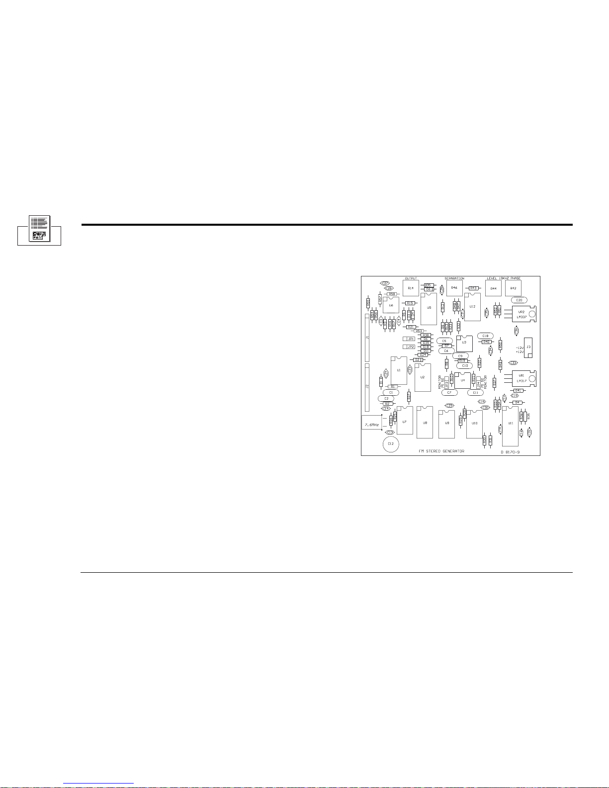
6–6
FM500 User's Manual
Illustration 6–6 Stereo Generator Board
Page 71
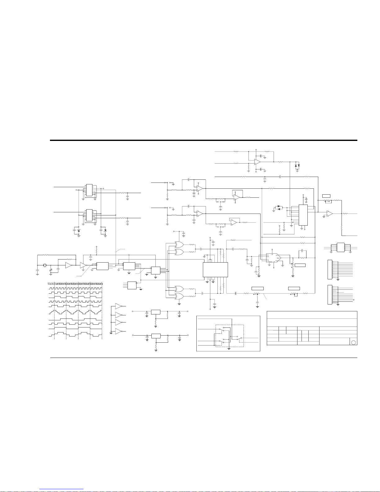
6–7
Reference Drawings
STEREO GENERATOR
OUTPUT
+12V
+6V
+12V
-12V
2
3
1
8
4
U4A
TL072
R12
10.0K
1%
R11
100
D3
R58
3.9K
R55
24.9K
C26
1.0
2
3
1
8
4
U6A
TL072
C27
1.0
R57
24.9K
R9
2K
1%
R56
24.9K 1%
R54
24.9K 1%
C3
100PF
R3
0 OHM
C4
0 OHM
R5
1K
(SELECTABLE BY TEST, USE
EXTERNAL COMPOSIT IN
(3.5V P-P for 7.5KHz)
(3.5V P-P for 75KHz)
+12V
-12V
C1
.0027
POLY
R38
1M
R6
499
1%
3
1
2
JP1
C5
.0027
POLY
R7
3.65K
1%
C6
1030PF
2
3
1
8
4
U3A
TL072
R1
330
15.2 KHz LOW-PASS FILTER
(8th ORDER ELLIPTICAL)
LPIN L
+6V
-6V
1
2
3
4
5
6
7
14
13
12
11
10
9
8
U1
LTC1064-1
14
7
+6V
R26
1K
Y1
7.6MHZ
C13
56PF
NPO
R25
1M
1
2
U7A
74HC04
C14
33PF
NPO
C29
1.0
R27
100
CK
1
CK
4
CLR
2
Q
3
Q
5
QC
6
QD
7
U8A
74HC390
13
12
U7F
C24
1.0
D1
1N5818
C23
1.0
D2
1N5818
1
2
3
4
5
6
7
14
13
12
11
10
9
8
U2
LTC1064-1
1.52 MHz
3.8 MHz
14
8
16
14
50 75
50 75
LPOUT R
INPUT R
+6V
+5.00V
CK
15
CK
12
CLR
14
QA
13
QB
11
QC
10
QD
9
U8B
74HC390
A
13
Q
11
Q
10
QC
9
QD 8CLR
12
U9B
74HC393
4
5
6
U10B
R29
100K
1%
C15
0.1
L
P
A
1
L
P
B
2
0
B
P
A
2
H
P
A
3
I
N
V
A
4
S
1
A
5
B
P
B
1
9
H
P
B
1
8
I
N
V
B
1
7
S
1
B
1
6
S
A
/
B
6
V
A
+
7
V
D
+
8
L
S
H
9
C
L
K
A
1
0
A
G
N
D
1
5
V
A
1
4
V
D
1
3
5
0
/
1
0
0
1
2
C
L
K
B
1
1
U11
LMF100
R33
10.0K
1%
C11
.01
POLY
C31
1.0
R28
243K
1%
C30
1.0
C2
.0027
POLY
R2
330
3
1
2
JP2
R18
499
1%
C9
.0027
POLY
R19
3.65K
1%
C10
1030PF
R39
1M
6
5
7
U3B
TL072
3 1
2
JP4
R8
4.99K
1%
3
1
2
JP3
C7
.01
POLY
R34
49.9K
1%
R20
4.99K
1%
R10
2.49K
1%
R22
2.49K
1%
1
2
3
U10A
74HC86
38 KHz
3.0VP-P
8
7
16
SEPARATION
(•3.85V P-P)
R204
1K
+12V
-12V
MON L
MON R
COMP METER
SYNC OUT
MONO/STEREO
/EXT ENABLE
+12V
+6V
-12V
-6V
-12V
C17
0.1
R37
1K
C18
.0027
POLY
R40
10K
7
9
1
12
13
2
10
14
311
U12
B-B 4214
R32
10K
C21
0.1
R47
20K
C37
OPEN
R48
4.3K
R17
100
R21
10K
R53
10K
6
5
7
U4B
TL072
R24
100
D6
X0
12
X1
13
Y0
2
Y1
1
Z0
5
Z1
3
INH
6
A
11
B
10
C
9
X
14
Y
15
Z
4
U5
74HC4053
C28
1.0
6
5
7
U6B
TL072
R16
100
R14
1K
R15
4.02K
1%
R13
24.9K
1%
R23
24.9K
1%
4.12K OR 4.15K IF NEEDED)
12
34
56
78
910
J3
RECEPT 5X2
19 KHz
3.3VP-P
19 KHZ LEVEL
STEREO
X1
EXTERNAL COMPOSITE
U205 Connections
X
SCA IN
COMP OUT
COMP METER
/EXT ENABLE
EXT IN
EXT RTN
GND
MONO/STEREO
U5Y
R43
33K
R41
510
1
2
3
4
5
6
7
8
9
10
11
12
J1
RECEPT 12X1
C19
0.1
C20
.0027
POLY
1.9MHz
304 Khz
7
7
+12V
-6V
+12V
+6V
C33
1.0UF
C34
1.0UF
R49
240
IN
1
C
2
OUT
3
VR1
LM317
C16
0.1
C32
1.0
R30
243K
1%
9
10
8
U10C
74HC86
12
13
11
U10D
A 1QA
3
QB
4
QC
5
QD
6
CLR
2
U9A
74HC393
R35
10.0K
1%
R36
49.9K
1%
R31
100K
1%
R50
910
7.6 MHz
CLK
QA
QB
QC
QD
QB XOR QD
QC XOR QD
QB XOR QC
QA XOR QC
Current at U211 pin 4.
Current at U211 pin 17.
-12V
-12V -6V
C35
1.0
IN
1
C
2
OUT
3
VR2
LM337
R52
910
R51
240
11
10
U7E
74HC04
9
8
U7D
74HC04
5
6
U7C
74HC04
3
4
U7B
74HC04
C36
47UF
MONO
STEREO/MONO
Z
C
X0
B
Y
A
Y1
Y0
Z1
Z0
MON L
MON R
+5.00V
SYNC OUT
INPUT L
INPUT R
GND
LPIN L
LPOUT L
LPIN R
LPOUT R
+5.00V
1
2
3
4
5
6
7
8
9
10
11
12
J2
RECEPT 12X1
U5X
U5Z
U206, pin6
/EXT EN
NOTES :
_______
_______
1. ALL RESISTORS ARE IN OHMS, 1/4W, 5% UNLESS OTHERWISE SPECIFIED.
2. ALL CAPACITORS ARE IN MICROFARADS UNLESSOTHERWISE SPECIFIED.
CROWN INTERNATIONAL, INC.
1718 WEST MISHAWAKA ROAD ELKHART, IN. 46517 PHONE (219) 294-8000
DO NOT SCALE PRINT
SUPERSEDES
REV
ME
EE
PE
APPROVED BY :DRAWN
CHECKED
SCALE NONE
PROJ #
DWG. NO.
E.C.
JFL
NEXT ASM:FILENAME:
A
SCM, FM STEREO GENERATOR
7-28-97
MLOWCM0
103203
103203A.SCM
3. ALL DIODES ARE 1N4148 UNLESS OTHERWISE SPECIFIED.
COMP OUT
LPIN R
LPOUT L
R242 1K
R244 10K
INPUT L
C12
5.5—18PF
EXT RTN
EXT IN
SCA IN
D4
D5
19 KHZ PHASE
R46
10K
JB
1
Page 72
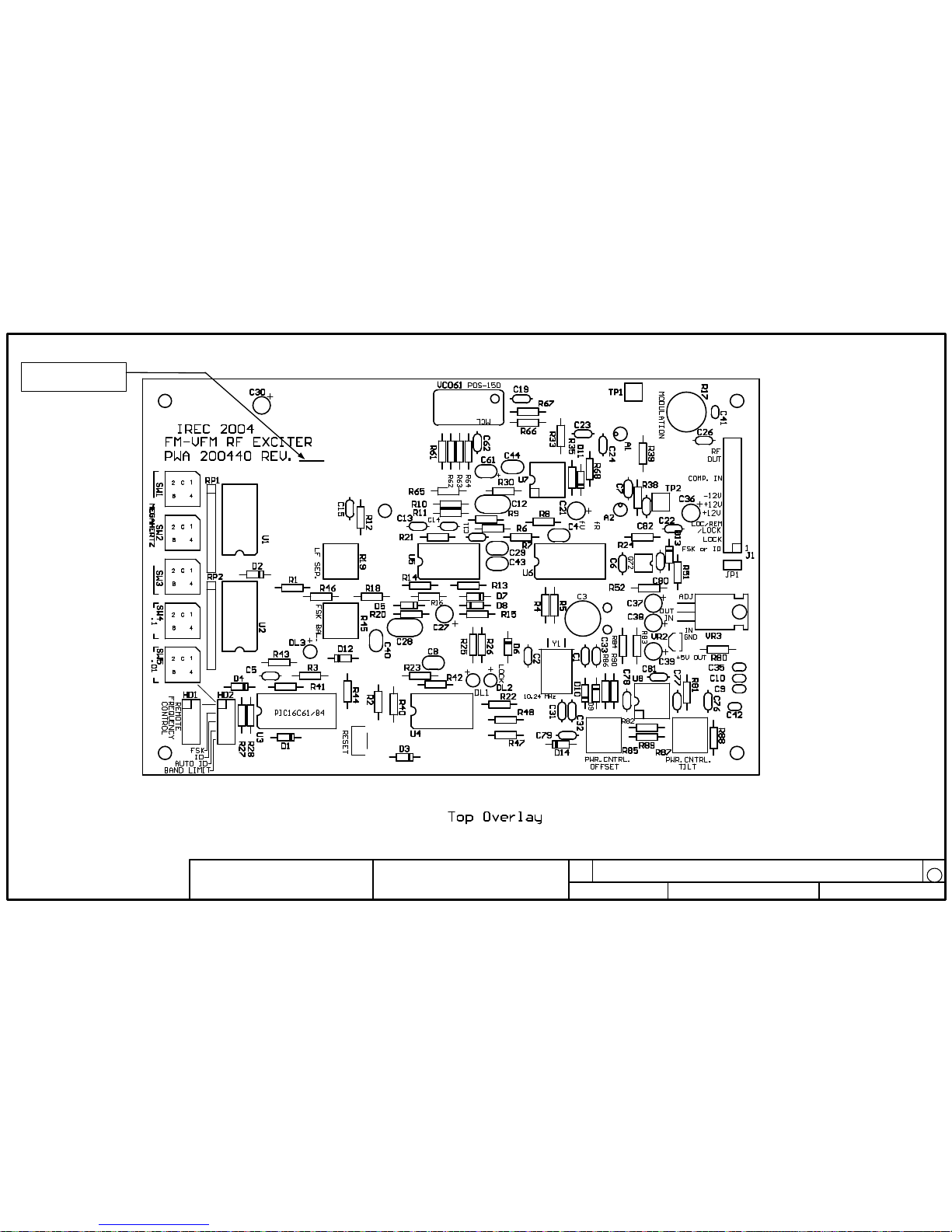
TOP SIDE COMPONENT MAP, FM-VFM EXCITER
UNCONTROLLED
UNLESS OTHERWISE MARKED IN RED BY CM AS A
CONTROLLED COPY, COPIES OF THESE DOCUMENTS AND
ASSOCIATED ELECTRONIC FILES ARE UNCONTROLLED AND
ARE FOR REFERENCE ONLY.
SIZE
B
DWG. NO.
200440
-
PWA
SCALE:
N/A
PROJECT #:
509
SHEET:
1 OF 1
PWB: 200440-PWB-A.PCB
M200440PT-A.DOC
REV
A
THESE DRAWINGS, SPECIFICATIONS AND ASSOCIATED
ELECTRONIC FILES ARE THE PROPERTY OF INTERNATIONAL
RADIO AND ELECTRONICS CORP., AND SHALL NOT BE REPRODUCED,
COPIED, OR USED AS THE BASIS FOR THE MANUFACTURE OR SALE OF
APPARATUS OR DEVICES WITHOUT PERMISSION.
SEE NOTE 10
Page 73
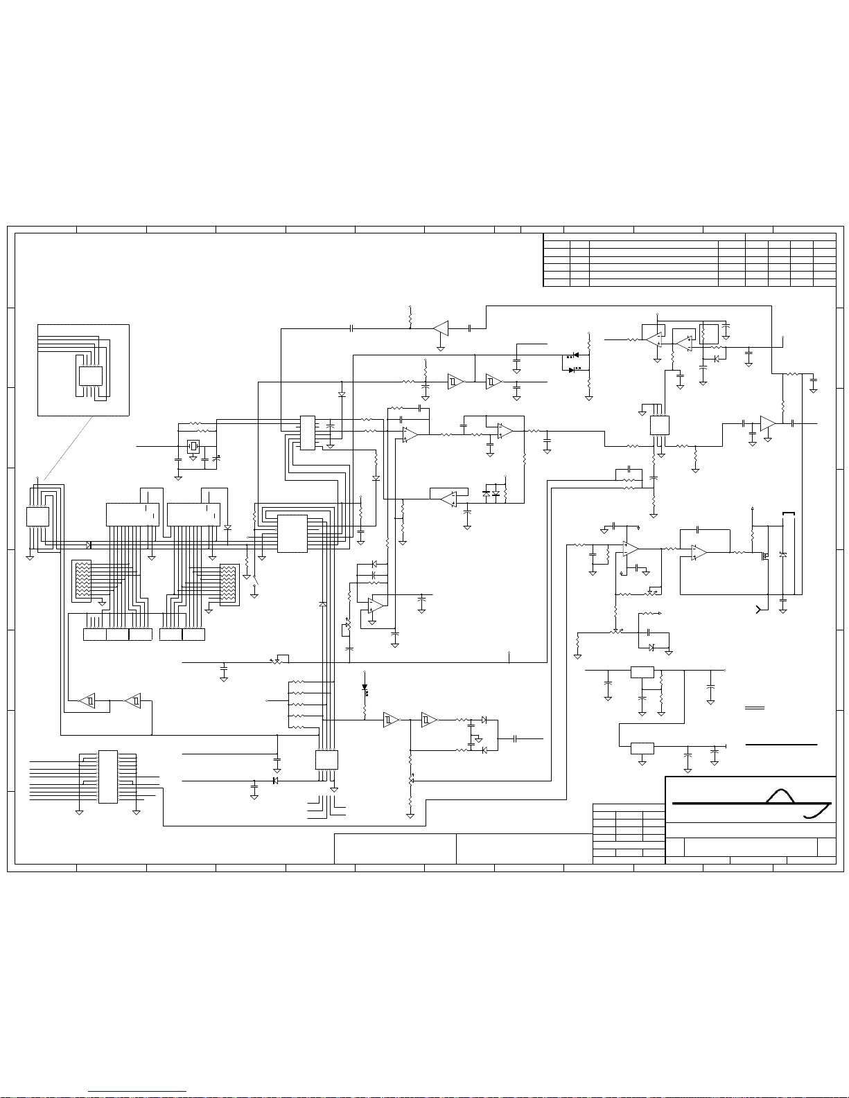
DWG. NO.
REV.
A
200440-SCH
H
G
F
E
D
C
B
A
1 2 3 4 5 6 7 8 9 10 11 12
H
G
F
E
D
C
B
A
1 2 3 4 5 6 8 9 10 11 12
E . C . N. REV DESCRIPTION
APPROVALS
PECHK CMDATE DWN
REVISION HISTORY
THESE DRAWINGS AND SPECIFICATIONS ARE THE
PROPERTY OF INTERNATIONAL RADIO CORP.
AND SHALL NOT BE REPRODUCED, COPIED OR USED AS
THE BASIS FOR THE MANUFACTURE OR SALE OF APPARATUS OR
DEVICES WITHOUT PERMISSION.
SHEET
OF
SCALE : NONE PROJ NO.FILENAME:
DWG . NO .
REV
A
200440-SCH
TITLE:
UNCONTROLLED
UNLESS OTHERWISE MARKED IN RED INK BY CM AS A
CONTROLLED COPY, COPIES OF THESE DOCUMENTS
INCLUDING ASSOCIATED ELECTRONIC REPRODUCTIONS
ARE FOR REFERENCE ONLY.
APPROVALS
DWN
CHK
CM
PE
DISTRIBUTION
K
SIZE
C
C_L_SHT1_A.DOT REV. A
INTERNATIONAL RADIO AND ELECTRONICS CORP.
25166 LEER DRIVE ELKHART, IN. 46514
574-262-8900
WWW.IREC1.COM
IREC
+12V
/LOCK
/LOCK
LOCK
+12V
GND
+5V
+5V
FSK-R
LOCK
COMPOSITE IN
TP1
+12V
RF OUT
+8V
FSK-R
88-108 MHZ
COMPOSITE IN
+8V
-12V-12V
CLK
DATA
LOAD
8.26V
+8V
+5V
DATA
LOAD
CLOCK
GND
+5V
REMOTE FREQUENCY CONTROL
FSK BAL.
LF SEP.
CLOCK
DATA
/ENABLE
OSC in
OSC out
Fin
VDD
VDD
+5V
+12V
VVCO
FSK
+5V
CH. SEL.
DIRECT FSK
+5V
LOCK DET.
+5V
VU5
VU5
+12V
FSK
Local/Remote
Local/Remote
Frequency Select
ID
AUTO ID
BAND LIMIT
FSK-ID-CHAN
TP
NOTES :
1. ALL RESISTORS ARE IN OHMS,
1/4W, 5% TOL.
2. ALL CAPACITORS ARE IN MICROFARADS.
DL1
GREEN
DL2
RED
IN
3
C
2
OUT
1
VR3
LM317
12
34
56
78
910
1112
1314
1516
1718
1920
2122
2324
2526
J1
RECEPT 13X2
12345
SW1
12345
SW3
12345
SW2
12345
SW4
12345
SW5
IN
3
C
2
OUT
1
VR2
LM78L05
PB1
RESET
SER10A11B12C13D14E3F4G5H
6
QH
9
CLK
2
QH
7
INH15SH/LD
1
U2
74HC165
SER10A11B12C13D14E3F4G5H
6
QH
9
CLK
2
QH
7
INH15SH/LD
1
U1
74HC165
12345678910
HD1
HEADER 5X2
1
2
3
4
5
6
7
8
9
10
RP1
100K RPACK
1
2
3
4
5
6
7
8
9
10
RP2
100K RPACK
R1
10.0K
RA2
1
RA3
2
RTC
3
CLR
4
VSS
5
RB0
6
RB1
7
RB2
8
RB39RB4
10
RB5
11
RB6
12
RB7
13
VDD
14
OSC2
15
OSC1
16
RA0
17
RA1
18
U3
PIC16C61
R2
10.0K
R17
1K BECKMAN
R18
68K
R19
25K
R24
150
R25
680
R26
680
R44
10.0K
R45
10K
R46
39K
R47
1.0K
R48
1.0K
R51
237
R52
1.27K
C1
33PF NPO
C2
39PF NPO
C3
1-10PF
C5
.001 POLY
C6
100PF
C7
.001
C9
.001
C10
.001
C13
3900PF
C19
.001
C23
.001
C26
.001
C31
.001
C32
.001
C33
33pF
C35
.001
D1
1N4148
D2
1N4148
D3
1N4148
D4
1N4148
D5 1N4148
D9
1N4148
D10
1N4148
R5
1.0K
R16
100K
R15
100K
D8
1N4148
C41
100PF
9 8
U4D
74HC14
5 6
U4C
74HC14
13 12
U4F
74HC14
11 10
U4E
74HC14
34
U4B
74HC14
12
U4A
74HC14
1
1
2
2
3
3
4
4
5
5
6
6
7
7
8
8
16
16
15
15
14
14
13
13
12
12
11
11
10
10
9
9
U6
MC145170
R4 100K
Y1
10.24MHZ
D7
1N4148
2 1
3
A2
MAR-6
C22
.001
R63
39
123456
78
VCO61
POS-150
DL3
AMBER
1 2
3 4
5 6
7 8
9 10
HD2
HEADER 5X2
R30
10
R43
1.0K
12345678910
PL1
HEADER 5X2
C24
33pF NPO
R7 10
C42
.001
C11 .001
C12
1
C14
.001 POLY
R6
100K
R9
100K
R10
100K
R11
100K
R13
100K
R14
100K
R21
100K
R12
1.0K
R62
100
R65
100K
R61
10.0K
R20 1M
R41 10.0K
R28 10.0K
R27 10.0K
R42 10.0K
R40 10.0K
R23
1M
R22
200K
C15
0.01
R35 499K
D12
1N4148
R3
150K
D6
1N4148
R66
150
R67
15
R68
499K
21
3
A1
MAR-6
R38
15
R39
100
R33
100
D11
1N4148
C62
220pF
R64 4.99K
2
3
1
411
U5A
MC33284P
6
5
7
U5B
MC33284P
9
10
8
U5C
MC33284P
13
12
14
U5D
MC33284P
2
3
1
84
U7A
NE5532
5
6
7
U7B
NE5532
+5V
GND
RF OUT
8
9
C4
1
C29
1
C43
1
C8
1
C44
1
C40
1
C28 1
509
2
3
1
8 4
U8A
TL072
5
6
7
U8B
TL072
C76
0.1
C77
0.1
C78 0.1
-12V
+12V
R85
2K
PWR. CNTRL. OFFSET
C79 0.1
-12V
R87
10K
Q72
IRFD9120
G
S
D
D13
3.9V
TP2
4.5 - 8.0V
1
2
JP1
JUMPER
C82
.01
PWR. CNTRL TILT
+8V
SCH, FM-VFM RF EXCITER
DW
01-04-02
R80
24.3K 1%
R88
30.1K 1%
R89
26.7K 1%
R82
24.3K 1%
R90
499 1%
R86
680.0
D14
6.2V 1N753A
R81
10.0K
C81
1000pF
R83
5.11K 1%
R84
5.11K 1%
C80
0.1
1 FOR PROTOTYPE 01-04-02 DW
02-06-02 DW2 MODIFIED PER MIKE SENEKI
06-24-02 DW3 CHG'D R18 PER EAD MRH01. R18 WAS 91K OHM. U5 WAS C 6900-5
1%
1%
1%
1%
1%
1%
1%
1%
1%
1%
1%
1%
1%
1%
1%
1%
1%
1%
1%
1%
1%
1%
1%
1%
1%
1%
1%
1%
1%
1%
1%
1%
1%
1%
1%
+
C61
47/20V
TANT.
+
C21
10/35V
TANT.
+
C27
10/35V
TANT.
+
C30
10/35V
TANT.
+
C36
10/35V
TANT.
+
C37
10/35V
TANT.
+
C38
10/35V
TANT.
+
C39
10/35V
TANT.
POLY
POLY
UNLESS OTHERWISE SPECIFIED:
1 1
REFERENCE DESIGNATORS NOT USED:
C16, C17, C18, C20, C25, C34, C45-60, C63-75,
Q1-71, R29, R31, R32, R34, R36, R37, R49, R50,
R53-60, R69-79, VCO1-VCO60.
R8
100
05-23-03 DW4 R8 WAS 1.0K OHM.
246 A-G
01-29-04 DWA PRODUCTION RELEASE
277
DW DP
DJ
01-05-02
DW
01-05-02
DP
01-05-02
Page 74
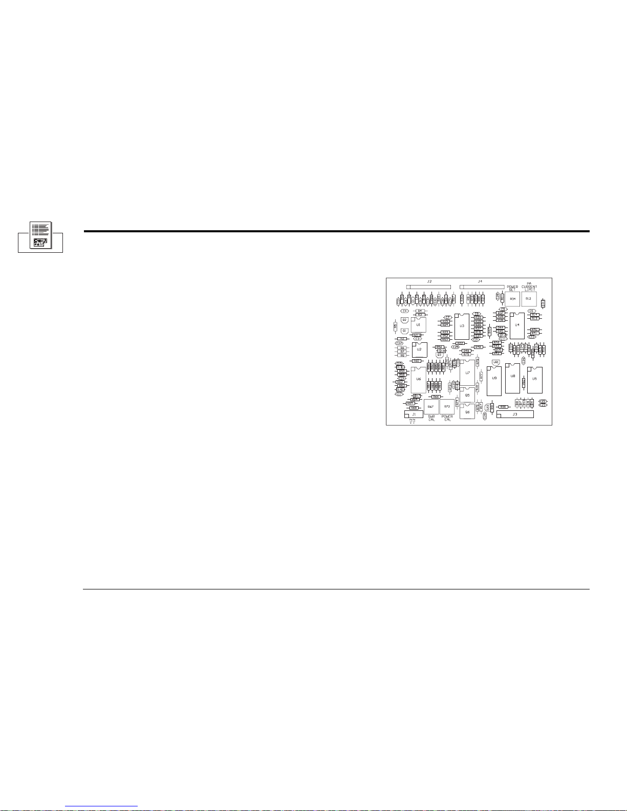
6–10
FM500 User's Manual
Illustration 6–8 RF Metering Board
(Add 400 to component designators for schematic reference)
D 8169-1
Page 75
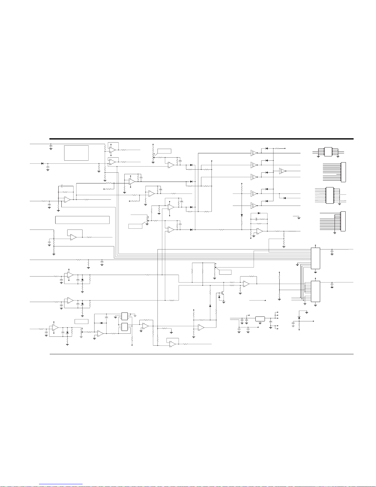
6–11
Reference Drawings
METERING
FAULT SUM
SWR LAMP
PADC LAMP
LOCK LAMP
+5V
PATEMP LAMP
R450
10K
D411
J2-1
J4-8
J3-18
J3-12
J3-14
J3-20
/+28V INH
11
10
U405E
74HC14
/LOCK
+5V
D406
D407
D408
D409
D410
U5
R416
100K
9
8
U405D
74HC14
13
12
U405F
74HC14
1
2
U405A
74HC14
3
4
U405B
74HC14
5
6
U405C
74HC14
R432
100K
R492
10K
+5V
J4-1
PAI LIMIT
+12V
1.00V = 10.0A
1.00V = 10VDC
FAN
REM PADCV
REM PADCA
R415
120K
C407
.001
C409
.001
D401
U3
U3
U4
U2
-12V
J2-7
J4-4
-12V
+12V
-12V
+12V +5.00V
6
5
7
U402B
TL072
2
3
1
8
4
U402A
TL072
R410
100
R409
100
R412
10K POT H
R411
15K
R413
33K
13
12
14
U404D
TL074
C405
.001
D402
R431
120K
2
3
1
4
1
1
U403A
TL074
13
12
14
U403D
TL074
2
3
1
4
1
1
U404A
TL074
R427
240K
R437
1M
R425
1M
R428
10K
R429
220K
R430
100K
C408
1.0UF
J4-3
R414
2.2M
R424
100k
R426
30.1K 1
5.00V = 100 deg. C
TEMP OUT
REM PATEMP
R418
1K
R420
100K 1
R421
100
R419
24.9K
U3
-12V
J2-4
J2-3
J2-6
J4-6
C421
.001
R407
10.0K 1
R406
100K 1
R423
240K
9
10
8
U403C
TL074
R408
1.1K 1
Parts not loaded:
R402, 403, 404
C403, 404
Q401, 402
DZ401
(Jumper under board)
C401
.01
U401
R405
2.49K 1
C431
0.1
PAV
LB401
R401
1N4148
C406
.01
PAI
50mv per degree C.
R422
75k
DC SUPPLY
SWR LIMIT=
(R435+R436)+R436
(R435+R436)-R436
---------------- = ----
150K
100K
= 1.5:1
VOLTMETER
10mV/Deg. C
REM BATT
R456
1K 1
U3
J2-2
J2-8
J4-7
R453
1.1K 1
R452
10K 1
R451
100K 1
R454
100
6
5
7
U403B
TL074
C412
0.1
C413
0.1
R455
100K 1
-12V
POWER SET
.001V per Watt
1mV/Degree C
10mV/Volt
100mV/Amp
10mV/Volt
10mV/Volt
RF LEVEL
C410
0.1
R441
1M
D403
U4
U4
J3-8
R438
120K
R435
100K
R436
24.9K
R440
33K
R434
10K POT H
9
10
8
U404C
TL074
D404
(VFWD+VREFL)/40
RF POWER (RFV SQUARED) RF POWER
SWR
ALC
PA DCV
PA DCI
PA TEMPERATURE
SUPPLY DC VOLTS
VOLTMETER
INPUT
R467
1K POTH
D412
C411
0.1
U4
-12V
J2-12
R445 100K
R446
10K
6
5
7
U404B
TL074
D405
R439
100K
R442
51K
R444
200K
R443
51K
ALC
DPM IN
+5V
16
FULL SCALE
1999 WATTS
19.99
19.99V
199.9V
19.99A
199.9V
199.9V
199.9 Deg. C
(1.999V reads "1999")
INPUT LAMP
U8
J3-19
GND
J3-16
R449
11K 1
R448
100K 1
R447
1K
C422
0.1
X0
13
X1
14
X2
15
X3
12
X4
1
X5
5
X6
2
X7
4
INH
6
A
11
B
10
C
9
X
3
U408
74HC4051
J4-2
1.00V
SEL A
SEL B
SEL C
DPM REF
+5V
VCC
VSS
VDD
VEE
8
8
+5V
16
R1-91
NUMBERS USED:
C1-29
U9
J3-2
J3-4
J3-6
J3-17
-12V
U8,9 pin 7
R417
3.3K
+5.00V
(C2)
DZ402
LM329DZ
-6.9V
X0
13
X1
14
X2
15
X3
12
X4
1
X5
5
X6
2
X7
4
INH
6
A
11
B
10
C
9
X
3
U409
74HC4051
C423
0.1
R490
10.0K 1
R491
2.49K 1
C429
1.0UF
C426
1.0UF
+12V
-12V
+12V
-12V
SWR CAL
(VFWD-VREFL)/4
+5V
R466
56K
R468
1K
R488
24.9K
R483
1M
R485
100K
U6
U6
J3-9,10
C424
1.0UF
C425
1.0UF
C428
1.0UF
+5.00V
+5.00V
13
12
14
U406D
TL074
R486
100K
R487
100K
R489
24.9K
Q403
2N5210
R484
10K
D417
R481
39K
9
10
8
U406C
TL074
R482
1K
D418
C427
1.0UF
IN
1
C
2
OUT
3
VR401
78L05
J4-12
C
B
E
C
B
E
C
B
E
C
B
E
(2.5VDC at 100W)
(.135V)
R474
3.3K
R476
49.9K
U7
R465
56K
9
10
8
U407C
TL074
R477
7.5K
R460
1K
R464
1K
1
1
2
2
3
3
4
4
8
8
7
7
6
6
5
5
Q405
LM394
1
1
2
2
3
3
4
4
8
8
7
7
6
6
5
5
Q406
LM394
RFV
RF REV
RF FWD
-12V
+12V
-12V
+12V
POWER CAL
R457
10K
R458
22K
R459
100K
R461
10K
R462
22K
R463
100K
R469
10K
R471
100K
C414
.01
C416
.01
C418
.01
D416
U6
U6
U7
U7
D413
1N6263
J2-9
J2-10
J2-11
2
3
1
4
1
1
U406A
TL074
C415
.001
6
5
7
U406B
TL074
C417
.001
D414
1N6263
2
3
1
4
1
1
U407A
TL074
C419
.001
D415
1N6263
R472
10K POT H
6
5
7
U407B
TL074
C420
.01
R473
10K
R470
22K
R480
100
U7
-6.9V
R478
10.0K 1
13
12
14
U407D
TL074
R479
1.1K 1
R475
49.9K
(Clamp SWR reading below 5W.)
(1.00V at 100W)
REM RFWATTS
J4-5
FM500
METERING
103204A
-12V -12V
+12V+12V
12
34
56
78
910
J401
RECEPT 5X2
/LOCK
ALC
FAULT SUM
+5.00V
REM PATEMP
REM PADCV
REM PADCA
REM RFWATTS
REM BATT
J4
1
2
3
4
5
6
7
8
9
10
11
12
J404
RECEPT 12X1
SEL A
SEL B
SEL C
DPM REF
SWR LAMP
PADC LAMP
LOCK LAMP
+5.00V
DPM IN
INPUT LAMP
PATEMP LAMP
RF LEVEL
J3
+5.00V
12
34
56
78
910
1112
1314
1516
1718
1920
HD403
HEADER 10X2
RFV
DC SUPPLY
RF FWD
RF REV
FAN
TEMP OUT
VOLTMETER
/+28V INH
J2
INPUT
1
2
3
4
5
6
7
8
9
10
11
12
J402
RECEPT 12X1
PAV
PAI
Page 76
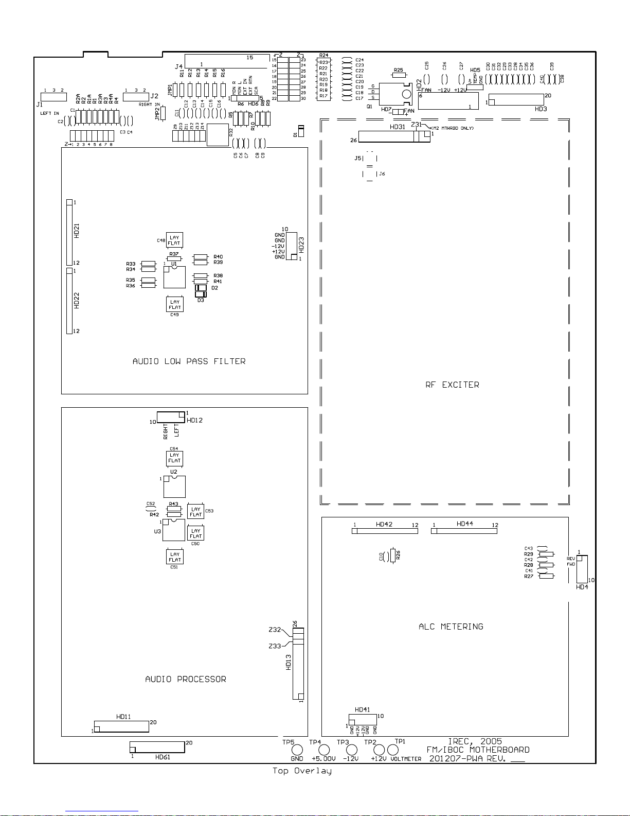
Page 77

1 2 3 4 5 6 7 8 9 10 11 12
A
B
C
D
E
F
G
H
121110987654321
H
G
F
E
D
C
B
A
DWG. NO. REV.
1
201207-SCH
E . C . N. REV DESCRIPTION
APPROVALS
PECHK CMDATE DWN
REVISION HISTORY
65
THESE DRAWINGS AND SPECIFICATIONS ARE THE
PROPERTY OF INTERNATIONAL RADIO AND ELECTRONICS CORP.
AND SHALL NOT BE REPRODUCED, COPIED OR USED AS
THE BASIS FOR THE MANUFACTURE OR SALE OF APPARATUS OR
DEVICES WITHOUT PERMISSION.
1 1SHEET OF
SCALE : NONE
PROJ NO.
FILENAME:
DWG . NO .
REV
1
201207-SCH
TITLE:
SCH, FM/IBOC MOTHER BOARD
UNCONTROLLED
UNLESS OTHERWISE MARKED IN RED INK BY CM AS A
CONTROLLED COPY, COPIES OF THESE DOCUMENTS
INCLUDING ASSOCIATED ELECTRONIC REPRODUCTIONS
ARE FOR REFERENCE ONLY.
APPROVALS
DWN
CHK
CM
PE
DISTRIBUTION
K
SIZE
D
Error : logo3A.jpg file not found.
INTERNATIONAL RADIO AND ELECTRONICS CORP.
25166 LEER DRIVE ELKHART, IN. 46514
574-262-8900
WWW.IREC1.COM
IREC
1 FOR PROTOTYPE 02-05-05 DW DW
1
9
2
10
3
11
4
12
5
13
6
14
7
15
8
J4
DB15
C17
.01
C18
.01
C19
.01
C20
.01
C21
.01
C22
.01
C23
.01
C24
.01
R24 220
C38
OPEN
C39
OPEN
C40
OPEN
R13 390
R14
390
R12 1K
R11 220
R15 100
R16 220
C11
.01
C12
OPEN
C13
.001
C14
.001
C15
.01
C16
.01
C30
.01
C31
.01
C32
.01
C33
.01
C34
.01
C35
.01
C36
.01
1
2
3
HD5
HEADER 3X1
123
J2
OPEN
C3
220pFC4220pF
C5
220pF
C6
220pF
C7
220pF
C8
220pF
C9
220pF
R3
1K
R4
1K
R51KR61KR7
1K
R81KR9
1K
R10
240
12345
HD6
OPEN
2
3
1
REF. FOR
XLR CON.
HI
LO
GND
SCA
EXT_RTN
EXT_IN
MON_L
MON_R
-12V
+12V
12345678910111213141516171819202122232425
26
HD31
26 HEADER
J5
MCXJ6MCX
J1
12345678910111213141516171819202122232425
26
RFX OUT
1234567891011
12
HD42
HEADER 12
1234567891011
12
HD44
HEADER 12
J2J4
1234567891011
12
+5.00V
D1
1N4148
123456789
10
HD41
HEADER 5 x 2
J1
V+
TEMP
GND
R27
1K
R28 1K
R29
1K
1
2
3
4
5
6
7
8
9
10
HD4
HEADER 5 x 2
1
2
3
4
5
6
7
8
9
10
11
12
HD21
HEADER 12
1
2
3
4
5
6
7
8
9
10
11
12
HD22
HEADER 12
+5.00V
LEFT
RIGHT
R IN2
R IN1
L IN2
L IN1
LPIN L
LPOUT L
LPIN R
LPOUT R
+12V
-12V
L VU
+5.00V
PROC A
PROC B
PROC C
R VU
BR GR
HI GR
1234567891011
12
ALC / METERING
1
2
3
4
5
6
7
8
9
10
11
12
13
14
15
16
17
18
19
20
HD3
HEADER 10 x 2
+12V
123456789
10
+12V
-12V
C41
.001
C42
.001
C43
.001
RF EXCITER
C10
.01
R26
1K
TP1
VOLTMETER
1
2
3
4
5
6
HD2
HEADER 6X1 .156
+12V
1
2
HD7
HEADER 2 .156
C25
.01
C26
.01
C27
.01
R25
OPEN
Q1
IRF541
R4A
300
R3A
300
Z8
OPEN
Z7
OPEN
123
J1
XLR
C1
220pFC2220pF
R1
1K
R2
1K
R2A
300
R1A
300
Z3
OPEN
Z5
OPEN
Z4 OPEN
Z6 OPEN
Z1
JUMPERZ2JUMPER
J1
1
2
3
4
5
6
7
8
9
10
11
12
STEREO GENERATOR
J2
1
2
3
4
5
6
7
8
9
10
11
12 1
2
3
4
5
6
7
8
9
10
HD23
HEADER 5 x 2
J3
1
2
3
4
5
6
7
8
9
10
+12V
-12V
SCA IN
EXT RTN
EXT IN
/EXT ENABLE
COMP OUT
RIGHT
LEFT
MON R
MON L
LPIN L
LPOUT L
LPIN R
LPOUT R
1
2
3
4
5
6
7
8
9
10
11
12
13
14
15
16
17
18
19
20
HD11
HEADER 10 x 2
J1
1
2
3
4
5
6
7
8
9
10
11
12
13
14
15
16
17
18
19
20
AUDIO PROCESSOR
1
2
3
4
5
6
7
8
9
10
HD12
HEADER 5 x 2
J2
1
2
3
4
5
6
7
8
9
10
1
2
3
4
5
6
7
8
9
10
11
12
13
14
15
16
17
18
19
20
21
22
23
24
25
26
HD13
HEADER 13 x 2
J3
1
2
3
4
5
6
7
8
9
10
11
12
13
14
15
16
17
18
19
20
21
22
23
24
25
26
+12V
-12V
/+6DB
/+12DB
+5.00V
COMP METERCOMP METER
COMP METERCOMP METER
STEREO/MON
STEREO/MON
1
2
3
4
5
6
7
8
9
10
11
12
13
14
15
16
17
18
19
20
HD61
HEADER 10 x 2
ALC
ALC
ALC
ALC
ALC
FAN
TP2
+12V
+12V
TP3
-12V
+12V
TP4
+12V
+5.00V
TP5
GND
2
3
1
U1A
TL072
C48
1.0
+12V
C49
1.0
-12V
R33
24.9K
1%
R34 24.9K 1%
R36
24.9K
1%
R35
24.9K
1%
Z11
OPEN
EXT RTN
Z10
OPEN
R37
3.9K
5
6
7
U1B
TL072
R32
1K
EXT IN
R41 1K
Z14
OPEN
SCA IN
D2
1N4148
D3
1N4148
R38
4.02K
1%
R39
100
R40
100
Z12
OPEN
Z13
OPEN
COMP METER
COMP OUT
COMP OUT
STEREO GENERATOR SHUNT
NC
1
Vin
2
TEMP
3
GND4TRM
5
Vout
6
NC
7
NC
8
U2
REF02
+12V
C54
1.0
2
3
1
U3A
TL072
C50
1.0
+12V
C51
1.0
-12V
5
6
7
U3B
TL072
R43
100
C52
.01
R42
4.7K
C54
1.0
Z9
OPEN
+5.00V
AUDIO PROCESSOR SHUNT
_METER PAV
_METER PAI
_METER RFW
_METER PA TEMP
_METER BATT
_FAULT SUM
_/AUTO CAR. OFF
_/CARRIER OFF
_FSK IN
_ALC
_COMPOSITE OUT
_38 KHZ OUT
_/EXT ENABLE
L IN1
L IN2
R IN1
R IN2
R IN1
L IN2
JMP1 OPEN
JMP2 OPEN
R23 220
R22 220
R21 220
R20 220
R19 220
R18 220
R17 220
FAULT SUM
FAULT SUM
METER BATT
METER BATT
METER PATEMP
METER PATEMP
METER RFW
METER RFW
METER PAI
METER PAI
METER PAV
METER PAV
ALC
FSK IN
FSK IN
FSK IN
NC
NC
NC
NC
NC
NC
PAI
PAV
/LOCK FAULT
C28
.001
C29
.001
DC SUPPLY
TEMP
TEMP
INPUT
INPUT
FAN+12V
FAN
V-METER
RFV
RF FWD
RF REV
/LOCK
/LOCK
/LOCK
NC
NC
NC
38KHZ38KHZ
NC
NC
NC
NC
NC
NOTES:
UNLESS OTHERWISE SPECIFIED:
1. ALL RESISTORS ARE IN OHMS, 1/4W, 5% TOL.
2. ALL CAPACITORS ARE IN MICROFARADS.
DW 11-23-04
DW 11-23-04
/EXT ENABLE
/EXT ENABLE
COMP METER
INPUT CONFIGURATION CHART
NON-OMNIA BOARD INPUT IMPEDENCE
Z1, Z2 ON
Z3, Z5, Z7, Z8 OFF
Z4, Z6 OFF
50 KOHM
Z1, Z2 ON
Z3, Z5, Z7, Z8 ON
Z4, Z6 OFF
600 OHM
OMNIA BOARD AES/EBU INPUT
Z1, Z2 OFF
Z3, Z5, Z7, Z8 OFF
Z4, Z6 ON
ANALOG LEFT/RIGHT
LEFT IN 1 LEFT IN 2
Z32
OPEN
Z33
OPEN
Z31
OPEN
ADD FOR M2HD-S
MOTHERBOARD ONLY
INSTALLED WHEN USING
AUDIO PROC. SHUNT CKT.
Z15 OPEN
Z16 OPEN
Z17 OPEN
Z18 OPEN
Z19 OPEN
Z20 OPEN
Z21 OPEN
Z22 OPEN
Z23
JUMPER
Z24
JUMPER
Z25
JUMPER
Z26
JUMPER
Z27
JUMPER
Z28
JUMPER
Z29
JUMPER
Z30
JUMPER
Page 78
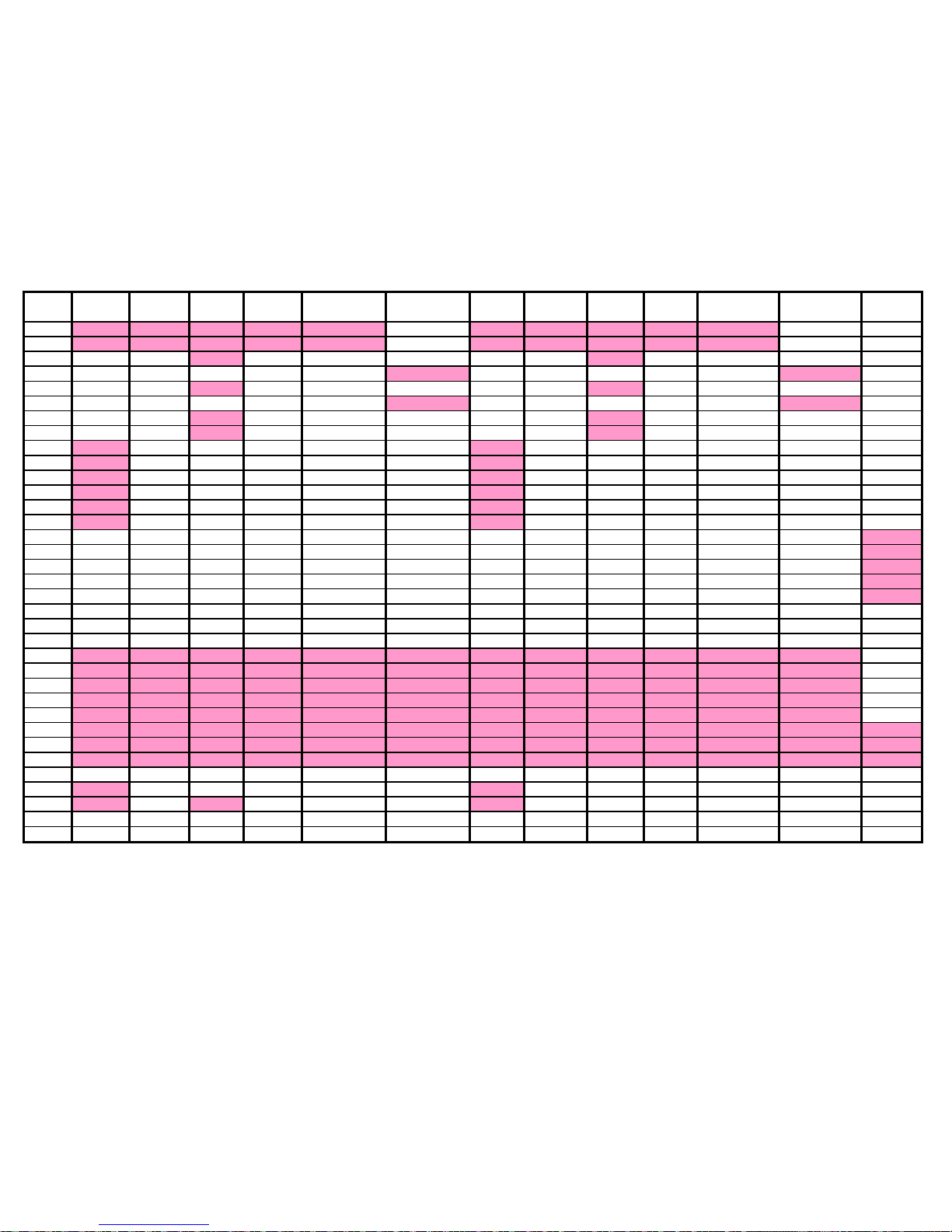
Jumper FMA "E" FMA "T" FMA"T" FMA "R" FMA "Omnia" FMA "Omnia" FMX "E" FMX "T" FMX "T" FMX "R" FMX "Omnia" FMX "Omnia" FMX
50K input 600 input Analog input AES input 50K input 600 input Analog input AES input RMS
Z1 Short Short Short Short Short Open Short Short Short Short Short Open
Z2 Short Short Short Short Short Open Short Short Short Short Short Open
Z3 Open Open Short Open Open Open Open Open Short Open Open Open
Z4 Open Open Open Open Open Short Open Open Open Open Open Short
Z5 Open Open Short Open Open Open Open Open Short Open Open Open
Z6 Open Open Open Open Open Short Open Open Open Open Open Short
Z7 Open Open Short Open Open Open Open Open Short Open Open Open
Z8 Open Open Short Open Open Open Open Open Short Open Open Open
Z9 Short Open Open Open Open Open Short Open Open Open Open Open
Z10 Short Open Open Open Open Open Short Open Open Open Open Open
Z11 Short Open Open Open Open Open Short Open Open Open Open Open
Z12 Short Open Open Open Open Open Short Open Open Open Open Open
Z13 Short Open Open Open Open Open Short Open Open Open Open Open
Z14 Short Open Open Open Open Open Short Open Open Open Open Open
Z15 Open Open Open Open Open Open Open Open Open Open Open Open Short
Z16 Open Open Open Open Open Open Open Open Open Open Open Open Short
Z17 Open Open Open Open Open Open Open Open Open Open Open Open Short
Z18 Open Open Open Open Open Open Open Open Open Open Open Open Short
Z19 Open Open Open Open Open Open Open Open Open Open Open Open Short
Z20 Open Open Open Open Open Open Open Open Open Open Open Open Open
Z21 Open Open Open Open Open Open Open Open Open Open Open Open Open
Z22 Open Open Open Open Open Open Open Open Open Open Open Open Open
Z23 Short Short Short Short Short Short Short Short Short Short Short Short Open
Z24 Short Short Short Short Short Short Short Short Short Short Short Short Open
Z25 Short Short Short Short Short Short Short Short Short Short Short Short Open
Z26 Short Short Short Short Short Short Short Short Short Short Short Short Open
Z27 Short Short Short Short Short Short Short Short Short Short Short Short Open
Z28 Short Short Short Short Short Short Short Short Short Short Short Short Short
Z29 Short Short Short Short Short Short Short Short Short Short Short Short Short
Z30 Short Short Short Short Short Short Short Short Short Short Short Short Short
Z31 Open Open Open Open Open Open Open Open Open Open Open Open
Z32 Short Open Open Open Open Open Short Open Open Open Open Open
Z33 Short Open Open Open Open Open Short Open Open Open Open Open
JMP1 Open Open Open Open Open Open Open Open Open Open Open Open Open
JMP2
Open
Open
Open
Open
Open
Open
Open
Open
Open
Open
Open
Open
Open
Page 79
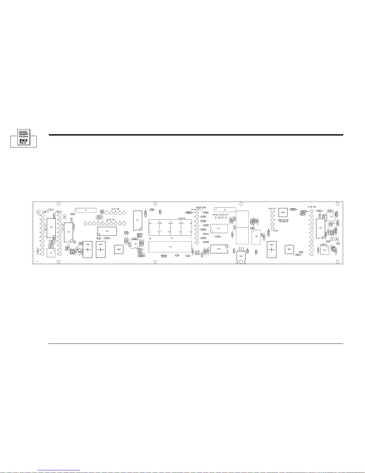
6–14
FM500 User's Manual
Illustration 6–10 Display Board
(Add 600 to component designators for schematic reference)
R27
D 8167-5
Page 80

6–15
Reference Drawings
"110"
RED
GRN
GRN
GRN
GRN
GRN
GRN
+5V
+12V
5.00V
+12V
+12V
C628
1.0UF
L2
18
L3
17
L4
16
L5
15
L6
14
L7
13
L8
12
L9
11
L1010MODE
9
RADJ
8
ROUT
7
DHI
6
L1
1
V-
2
V+
3
DLO
4
IN
5
U608
LM3914
YEL
6
5
7
U613B
TL072
FOR BAR
DL648-658
JP603
JUMPER
2
3
1
8
4
U613A
TL072
R647
1K
R648
1K
R627
2.7K
R652
5.6K
COMPOSITE
-12V
C611
0.1
+12V
R646
10M
Q603
2N5210
Q604
2N5087
R644
33K
R645
100
+12V
R653
1K
2
3
1
8
4
U607A
TL072
D606
1N6263
D618
C626
1.0UF
R623
10.0K
D605
1N6263
6
5
7
U607B
TL072
R643
3.3M
R622
10.0K
50mA
RED
GRN
GRN
GRN
GRN
GRN
GRN
GRN
RED
+5V
+5V
+12V
5.00V
L
2
1
8
L
3
1
7
L
4
1
6
L
5
1
5
L
6
1
4
L
7
1
3
L
8
1
2
L
9
1
1
L
1
0
1
0
M
O
D
E
9
R
A
D
J
8
R
O
U
T
7
D
H
I
6
L
1
1
V
2
V
+
3
D
L
O
4
I
N
5
U604 LM3914
HI GR
G GG G Y
YEL
DL621-625
DL601-610
R614
1.2K
Q601
MPS-A56
R605
1K
R613
1K
R606
330
C602
1.0UF
L VU
+12V
5.00V
+12V
+12V
-12V
D601
1N4148
D602
1N4148
JP601
R602
100K
R601
68K
C601
1.0UF
2
3
1
8
4
U601A
TL072
R603
1K
L2
18
L3
17
L4
16
L5
15
L6
14
L7
13
L8
12
L9
11
L1010MODE
9
RADJ
8
ROUT
7
DHI
6
L1
1
V-
2
V+
3
DLO
4
IN
5
U602
LM3915
R604
1.2K
C604
1.0UF
R609
1K
R VU
+12V
5.00V
+12V
+5V
R607
68K
C603
1.0UF
D604
1N4148
D603
1N4148
R608
100K
JP602
R610
1.2K
6
5
7
U601B
TL072
L2
18
L3
17
L4
16
L5
15
L6
14
L7
13
L8
12
L9
11
L1010MODE
9
RADJ
8
ROUT
7
DHI
6
L1
1
V-
2
V+
3
DLO
4
IN
5
U603
LM3915
50mA
DL11-20
RED
GRN
GRN
GRN
GRN
GRN
GRN
GRN
RED
C607
0.1
C608
.001
R617
1K
DITHER
+5V
+5V
+12V
5.00V
L
2
1
8
L
3
1
7
L
4
1
6
L
5
1
5
L
6
1
4
L
7
1
3
L
8
1
2
L
9
1
1
L
1
0
1
0
M
O
D
E
9
R
A
D
J
8
R
O
U
T
7
D
H
I
6
L
1
1
V
2
V
+
3
D
L
O
4
I
N
5
U605 LM3914
BR GR
R618
1.2K
Y Y G G G
G G G Y
YEL
R615
33K
R616
33K
C606
0.1
R611
1K
C605
.001
Q602
MPS-A56
R612
330
D607
-12V
MOD. CAL.
C610
0.1
R655
4.7K
R649
10K POT H
C612
.001
DL626-635
R624
1M
RED
R625
10K
"PILOT"
GRN
GRN
GRN
ST/MON
/+6DB
/+12DB
+5V
DITHER
C625
0.1
-12V
STEREO
MONO
R626
33K
5.00V
RF LEVEL
R629
680
SW603
SW601
SW602
C634
1.0UF
R657
1K BECKMAN
DP10
DP100
-12V
R651
2.2K
UNITSTENS100's1000
+5V
+5V
1234567891011121314151617181920
212223242526272829303132333435363738394
0
DL101
DISPLAY
1234567891011121314151617181920
212223242526272829303132333435363738394
0
U612
ICL7107
C614
0.1
C615
0.1
R638
100K
DPM IN
DPM REF
C617
0.1
R637
470K
C616
0.1 POLY
C618
0.1
C619
100PF
R635
100K
R636
100K
C627
1.0UF
DZ601
6.2V
SCM, FM DISPLAY
103206
SWR
SWR LAMP
PADC LAMP
LOCK LAMP
R619
510
DL644-647, 659
INPUT
LOCK
INPUT
PA DC
DL644
RED
DL645
RED
DL646
RED
DL647
RED
1312
U609F
74HC14
R620
220K
C609
1.0UF
PATEMP LAMP
PA TEMP
DL659
RED
+5V
VCC
16
U10
U11
8
VEE
VSS
VDD
-12V
+12V
+12V
-12V
14
U9
7
C630
1.0UF
C631
1.0UF
C622
1.0UF
C624
1.0UF
C629
1.0UF
C623
1.0UF
IN
1
C
2
OUT
3
VR601
7805
+12V
2
3
1
8
4
U606A
TL072
R631
5.6K
D616
D617
10V P-P DITHER
DITHER
6
5
7
U606B
TL072
R633
33K
C613
.01
R634
5.1K
-12V
R632
620
5
6
U609C
74HC14
9
8
U609D
74HC14
11
10
U609E
74HC14
R630
150
X0
13
X1
14
X2
15
X3
12
X4
1
X5
5
X6
2
X7
4
INH
6
A
11
B
10
C
9
X
3
U611
74HC4051
SWR
ALC
RF POWER
PA DC VOLTS
PA DC AMPS
SUPPLY DC VOLTS
19.99
19.99
199.9
199.9
199.9
19.99
F.S.
DECIMAL POINT
GRN
GRN
GRN
GRN
GRN
GRN
GRN
DP100
DP10
GRN
+5V
1999
R656
220
DL636-643
PA TEMPERATURE
199.9VOLTMETER
UP
DOWN
R639
100K
R640
100K
+5V
SW605
SW606
R628
1K
R654
1K
+5V
1 2
U609A
74HC14
3
4
U609B
74HC14
A15QA
3
B1QB
2
C10QC
6
D9QD
7
UP
5
CO
12
DN
4
BO
13
LOAD
11
CLR
14
U610
74HC193
C620
.01
C632
.001
C621
.01
C633
.001
R641
10K
R642
10K
SEL A
SEL B
SEL C
PROC A
R650
100K
BECKMAN
PROC B
PROC C
L VU
R VU
HI GR
BR GR
PROC A
PROC B
PROC C
/+6DB
/+12DB
DPM IN
DPM REF
MON/ST
SWR LAMP
PADC LAMP
LOCK LAMP
COMPOSITE
-12V
-12V
RF LEVEL
+12V
+12V
-12V
5.00V
GND
5.00V
5.00V
5.00V
SEL A
SEL B
SEL C
+12V
INPUT
PATEMP LAMP
Pin 1, upper left from front of unit.
12
34
56
78
910
1112
1314
1516
1718
1920
J601
HEADER 10X2
12
34
56
78
910
1112
1314
1516
1718
1920
J602
HEADER 10X2
NOTES :
1. ALL RESISTORS ARE IN OHMS, 1/4W, 5% UNLESS OTHERWISE SPECIFIED.
2. ALL CAPACITORS ARE IN MICROF ARADS UNLESS O THER WISE SPECIFIED .
DISPLAY
Page 81
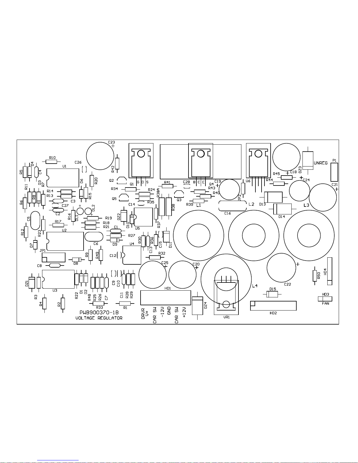
Page 82
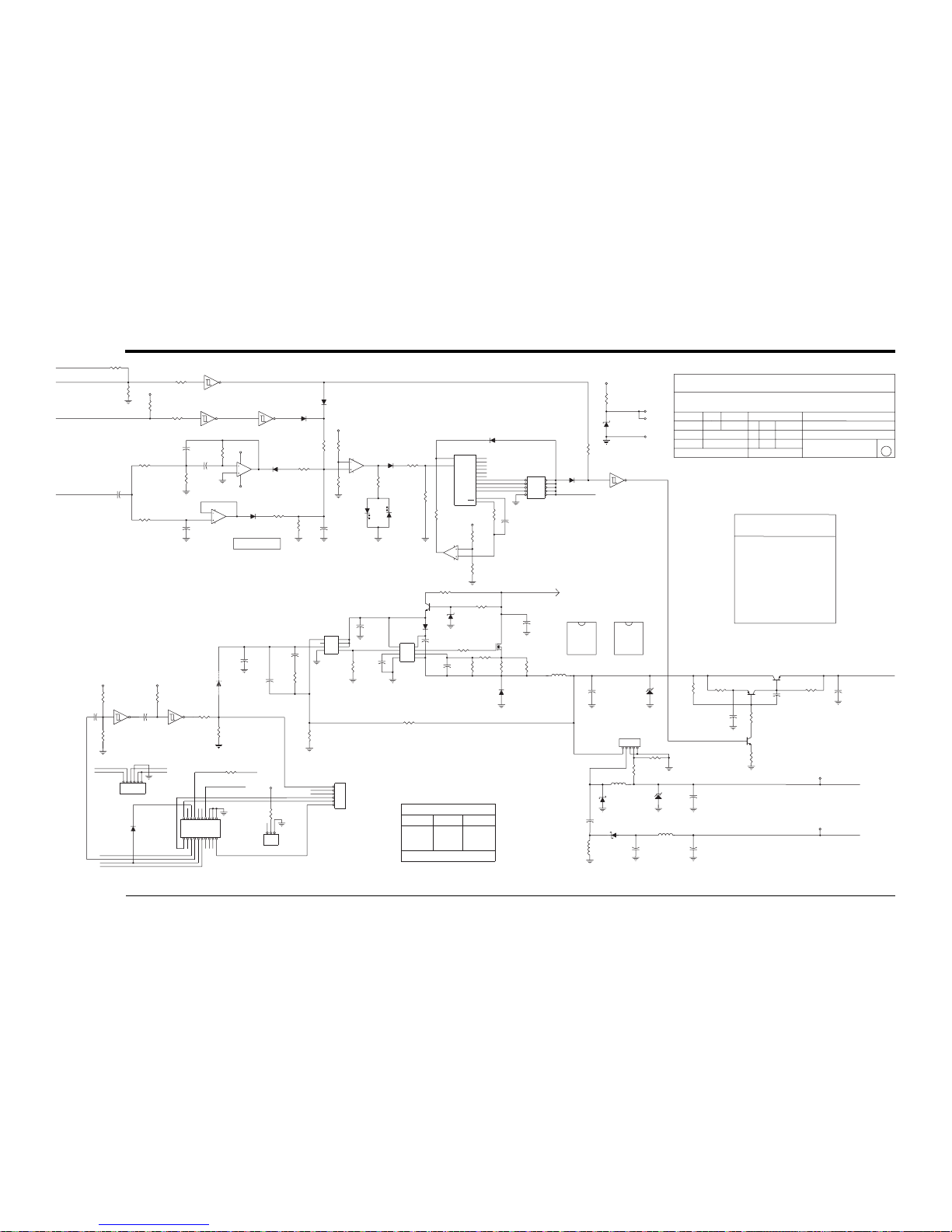
6–17
Reference Drawings
VOLTAGE REGULATOR
+6V
VDD
VSS
+12V
VCC
R723
1K
DZ701
1N4735
6.2V
R722
100K
R713
100K
D706
1N4148
+12V
R709
1K
R716
10K
D707
1N4148
PI
11
RST
12
Q4
7
Q5
5
Q6
4
Q7
6
Q8
14
Q9
13
Q10
15
Q12
1
Q13
2
Q14
3
PO
9
PO
10
U702
74HC4060
D702
1N4148
D701
1N4148
6
5
7
U701B
TL074
+12V
/CARRIER OFF
C703
.001
Fo=5KHZ BPF; Q=3
/AUTO CARRIER
VDD
5
6
U703C
74HC14
3
4
U703B
74HC14
1
2
U703A
74HC14
R702
10K
R704
10K
R707
180K
C702
.001
R705
91K
R701
4.7K
R703
4.7K
R733
4.7K
CARR SW
2
3
1
4
1
1
U701A
TL074
-12V
PROGRAM DETECT
VDD VDD
R725
100K
COMP2
AUDIO or COMPOSITE
R748
10K
D703
1N6263
R706
5.1K
R711
100K
C701
.01
C704
.001
13
12
U703F
74HC14
11
10
U703E
74HC14
D704
1N626313
12
14
U701D
TL074
R710
75K
1
1
2
3
4
+IN
OSC
GND
-IN
LM3578
U1
+UNREG
0.5
2
4
R715
2.2K
VDD
R720
10K
INPUT FAULT
R708
100K
R714
220
DL701
GREEN
R718
100K
12
34
56
78
910
JP701
HEADER 5X2
D708
1N4148
R717
10K
1
1
2
2
3
3
4
4
8
8
7
7
6
6
5
5
U705
IR2125
1
1
2
2
3
3
4
4
8
8
7
7
6
6
5
5
U704
LM3578
D710
1N4148
R735
51
C714
0.1
R724
100
R734
10K
TIME-OUT
SELECT
MINUTES
P701
8
Q701
IRF540
C723
330
100V
DZ702
1N9661B
16V
R712
1M
C706
1.0
POLY
C712
1.0
R719
10K
C705
1.0
POLY
Q705
MPSA06
DL702
RED
9
10
8
U701C
TL074
R721
24.9K
1
1
2
346
7
8VB
5
U2
6
7
8V+
5
CS
C
E
IR2125
VCC
IN
ERR
ESS VS
CS
OUT
28V ENABLE
9
8
U703D
74HC14
DRVR V+
+12V
-12V
+12V
R743
220
R739
510
R742
1K
Q704
MJE15028
R741
1K
(+13.5V)
(+12.5V)
DZ703
ICTE-12
DZ704
ICTE-12
C720
220UF
50V
C722
3300UF
16V
L702
960UH
C718
220
63V
C725
220
63V
R740
10
C719
1000
35V
Q702
MPSA06
Q703
MPSA56
C717
1UF
SYNC
ALC
DRVR V+
+UNREG
+12V
(TO POWER REG. BOARD)
R730
2.2K
R750
100
-12V
PAV
PAI
1
2
3
4
5
6
HD704
HEADER 6
L701
380UH
C711
.01
R728
68K
R729
4.12K
1
C713
100PF
R738A
1.0
0.5W
R738A
1.0
0.5W
R737
4.3K
R736
2K
C715
0.1
C724
47
20V
R751
JUMPER
A10124-22
D711
MUR110
D714
1N5822
R732
82.5K
1
/LOCK FAULT
METER UNREG
+12V
-12V
DRVR V+
INPUT FAULT
D715
1N4004
CARR SW
C709
2200PF
POLY
C710
56PF
NPO
123456
HD701
123456789
1
0
1
1
1
2
1
3
1
4
1
5
1
6
1
7
1
8
1
9
2
0
HD702
c 8667-5
38KHZ
COMP2
/CARRIER OFF
/AUTO CARRIER
FAN
L703
960UH
1 2 3
HD703
-12V
NOTES :
_______
_______
1. ALL RESISTORS ARE IN OHMS,
1/4W, 5% UNLESS OTHERWISE SPECIFIED.
2. ALL CAPACITORS ARE IN
MICROFARADS UNLESS OTHERWISE SPECIFIED.
THESE DRAWINGS AND SPECIFICATIONS ARE THE
SHALL NOT BE REPRODUCED, COPIED, OR USED
AS THE BASIS FOR THE MANUFACTURE OR SALE
OF APPARATUS OR DEVICES WITHOUT PERMISSION.
PROPERTY OF CROWN INTERNATIONAL, INC. AND
CROWN INTERNATIONAL, INC.
1718 WEST MISHAWAKA ROAD ELKHART, IN. 46517 PHONE (219) 294-8000
DO NOT SCALE PRINT
SUPERSEDES
REV
ME
EE
PE
APPROVED BY :DRAWN
CHECKED
SCALE NONE
PROJ #
DWG. NO.
E.C.
JFL
NEXT ASM:FILENAME: 10.SCM
A
103207
8-25-97
MLOWCMO
FM VOLTAGE REGULATOR
Inductor Data
L
Wire
Turn s
960uH
165
#26
380uH
#22
80
L701 L702-703
Micrometals T90 core
Remove:
U706
L704
R745
R744
C724
D713
D714 1N5822 to MUR110
Change: R732 100K to 49.9K
(C707)
(R726)
(R708)
(R749)
Add: 1UF/100V between L701 and L703 under board.
Modifications for use
with 12.5V RF driver.
DZ703 1.5KE36A to ICTE-12
C721, C722 3300UF to 220UF/50V
7912 regulator, using "L704" pads.
Jumper "U706" pads 1 and 2.
DZ705
C708
220 Pf
C707
.001
R726
100K
R749
1.5K
D709
OPEN
R727
620
1 2 3 4 5
LM2576–ADJ
U706
R745
10K 1%
D713
1N5822
R744
1.1K 1%
C721
3300UF
16V
L704
960UH
Page 83
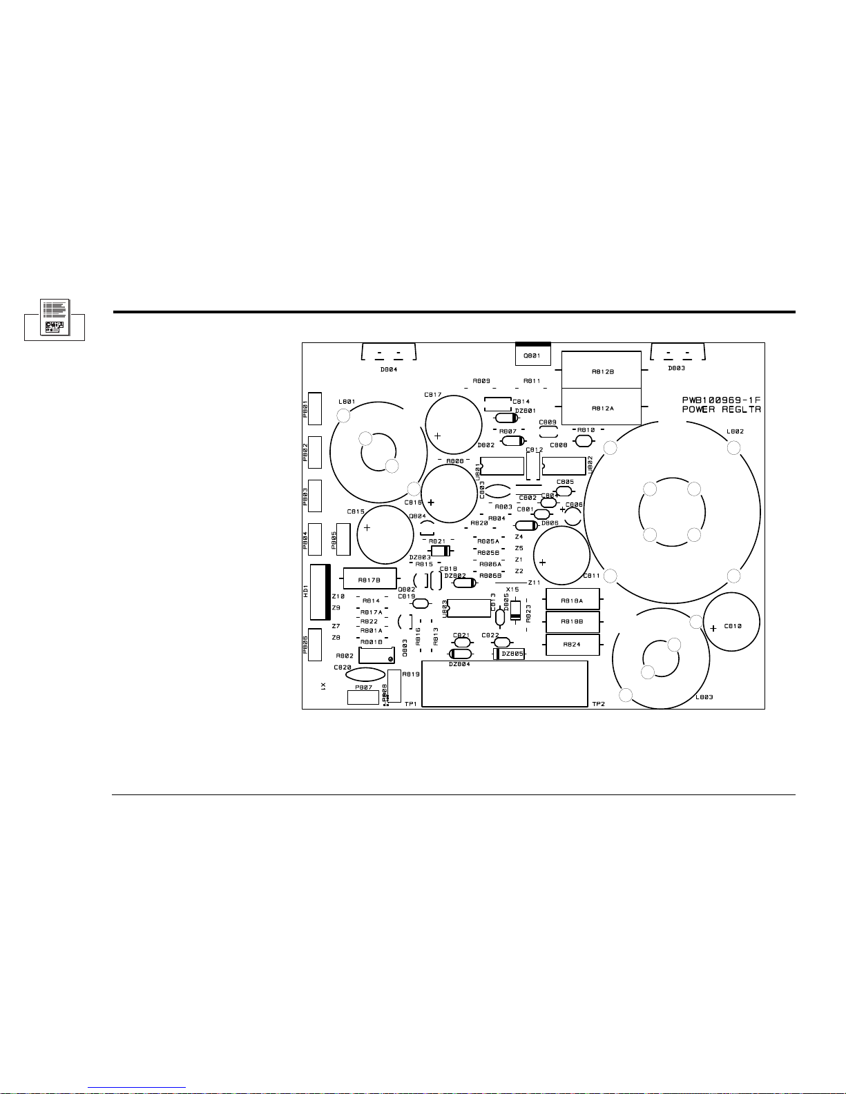
6–18
FM500 User's Manual
Illustration 6–12 Power Regulator Board
Page 84

DWG. NO. REV.
200915-SCH
C
1 2 3 4 7 8
A
B
C
D
E
F
1 2 3 4 6 7 8
A
B
C
E
F
5
THESE DRAWINGS AND SPECIFICATIONS ARE THE PROPERTY OF
INTERNATIONAL RADIO AND ELECTRONICS CORP.
AND ARE NOT TO BE REPRODUCED, COPIED OR USED AS THE BASIS
FOR THE MANUFACTURE OR SALE OF APPARATUS OR
DEVICES WITHOUT PERMISSION.
1 1
SHEET
OF
SCALE : NONE
PROJ NO.
FILENAME:
DWG . NO .
REV.
C
200915-SCH
TITLE:
SCH, FM POWER REGULATOR
UNCONTROLLED
UNLESS OTHERWISE MARKED IN RED INK BY CM AS A
CONTROLLED COPY, COPIES OF THESE DOCUMENTS
INCLUDING ASSOCIATED ELECTRONIC REPRODUCTIONS
ARE FOR REFERENCE ONLY.
APPROVALS
DWN
CHK
CM
PE
DISTRIBUTION
E . C . N. REV DESCRIPTION
APPROVALS
PECHK CMDATE DWN
REVISION HISTORY
65
SIZE
B
Error : logo3A.jpg file not found.
B_L_SHT1_A.DOT REV. A
INTERNATIONAL RADIO AND ELECTRONICS CORP.
25166 LEER DRIVE ELKHART, IN. 46514
574-262-8900
WWW.IREC1.COM
IREC
~
~
-
+
DC INPUT
TP1
TP2
ON CHASSIS
NOTES:
UNLESS OTHERWISE
SPECIFIED:
1. ALL RESISTORS ARE IN OHMS,
1/4W, 5% TOL.
2. ALL CAPACITORS ARE IN
MICROFARADS.
533
BATTERY
CIRCUIT BREAKER
110V
DW 09-30-03
R801B
24.9K
R801A
27.4K
1 2
Z7
1 2
Z6
1 2
Z9
1 2
Z8
12
Z1
12
Z2
R806A
330K
R805A
330K
R806B
200K
R805B
200K
D805
1N4148
R820
100K
R804
10.0K 1%
123
D803
BYV72EW-150
123
D804
BYV72EW-150
D802
1N4148
R811
ESS
4
ERR
3
IN
2
VCC1VB
8
OUT
7
CS
6
VS
5
U2
IR2125
GND
4
OSC
3
+IN
2
-IN1V+
8
CS
7
C
6
E
5
U801
LM3578AN
1
2
3
R802
10K
DZ801
1N966B 16V
DZ802
1N966B 16V
1 2
Z4
1 2
Z5
L801
30UH
L803
30UH
L802
*
Q801
IRF540
R808
1.0K
R809
51.0
R807
2.2K
R803
82K
R810
2.0K
R812A
0.1
R812B
0.1
DZ803
1N4735 6.2V
R821
10.0K
R818A
2.0K
R818B
2.0K
+
C815
330/100V
+
C816
330/100V
+
C817
330/100V
+
C810
330/100V
+
C811
330/100V
Q804
MPSA06
3
2
6
1
8
74
U803
OP-27GNB
Q802
MPSA56R814
22.0K
Q803
2N5087
R822
22.0K
R816
1.0K 1%
R813
1.0K
R815
100.0
R819
.04 OHM 15W 3%
R817B
2K
R817A
100
C1001
0.015F
C802
2200PF POLY
C801
220PF
C814
1/50V
C804
.01
C803
56PF
C813
.01UF
C819
.01UF
C820
0.01UF DISK
C809
.1
C818
.1UF
C805
100PF
C812
1/50V
C808
.0027
+
C806
4.7UF/63V
1
2
3
4
5
6
HD1
C 7527-2_6 HDR
P801
FASTON TAB
P802
FASTON TAB
P806
FASTON TAB
P803
FASTON TAB
P804
FASTON TAB
P805
FASTON TAB
P807
FASTON TAB
P808
FASTON TAB
PA-DC OUT
+ UNREG IN
C10582-2C10582-2C10582-2C10582-2
PWB_REV.G
PWB_100969-1
A PRODUCTION RELEASE 10-31-03 DW
R827
1.0K
1 2
Z3
DZ806
1N4735 6.2V
2W
2W
5W 5W
DZ807
1N966B 16V
R828
30K
REF DES
FM1
UNIT CONFIGURATION
SHORT
FM30 FM100 FM250 FM500
L802
OPEN
OPEN
OPEN OPEN
OPEN
OPEN OPEN
SHORT
SHORT
OPEN OPEN OPEN
OPEN OPEN SHORT SHORT SHORT
SHORT SHORT OPEN OPEN OPEN
SHORT SHORT SHORT SHORT OPEN
OPEN
OPEN
OPEN SHORTOPEN
H43608-1 H43395-5 H43533-1
H43533-1 H43533-1
*
*
*
*
*
*
*
*
*
*
*
*
*
2W
*
*
PA VOLTAGE SET
JUMPER
Z1
SHORT SHORT SHORT
Z2
SHORT
Z9
SHORT SHORT SHORT
Z8
Z7
Z6
Z4
Z5
Z3
SHORT SHORT SHORT SHORT SHORT
EURO
SHORT
OPEN
OPEN
OPEN
OPEN
SHORT
SHORT
SHORT
SHORT
H43533-1
HARRIS M1
SHORT
OPEN
OPEN
OPEN
OPEN
SHORT
SHORT
SHORT
OPEN
H43533-1
R811 5.11K 1%3.3K 3.3K 3.3K3.3K3.3K
R827
R828
DZ806
DZ807
OPEN
OPEN
OPEN
OPEN
OPEN
OPEN
OPEN
OPEN
OPEN
OPEN
OPEN
OPEN
OPEN
OPEN
OPEN
OPEN
OPEN
OPEN
OPEN
OPEN
OPEN
OPEN
OPEN
OPEN
INSTALLED
3.3K
HARRIS M2
OPEN
SHORT
OPEN
OPEN
SHORT
SHORT
SHORT
OPEN
OPEN
H43533-1
3.3K
INSTALLED
INSTALLED INSTALLED
INSTALLED INSTALLED
INSTALLED INSTALLED
DW 09-30-03
DP 09-30-03
200915-SCH
DW DP
B CORRECTED Z3 AND Z6 UNIT STATUS FOR M2 AND FM100 01-29-04 DW DW DP274
C SWAPPED Z1, Z2 TO MATCH PWB 08-10-04 DW DW323 DP
Page 85
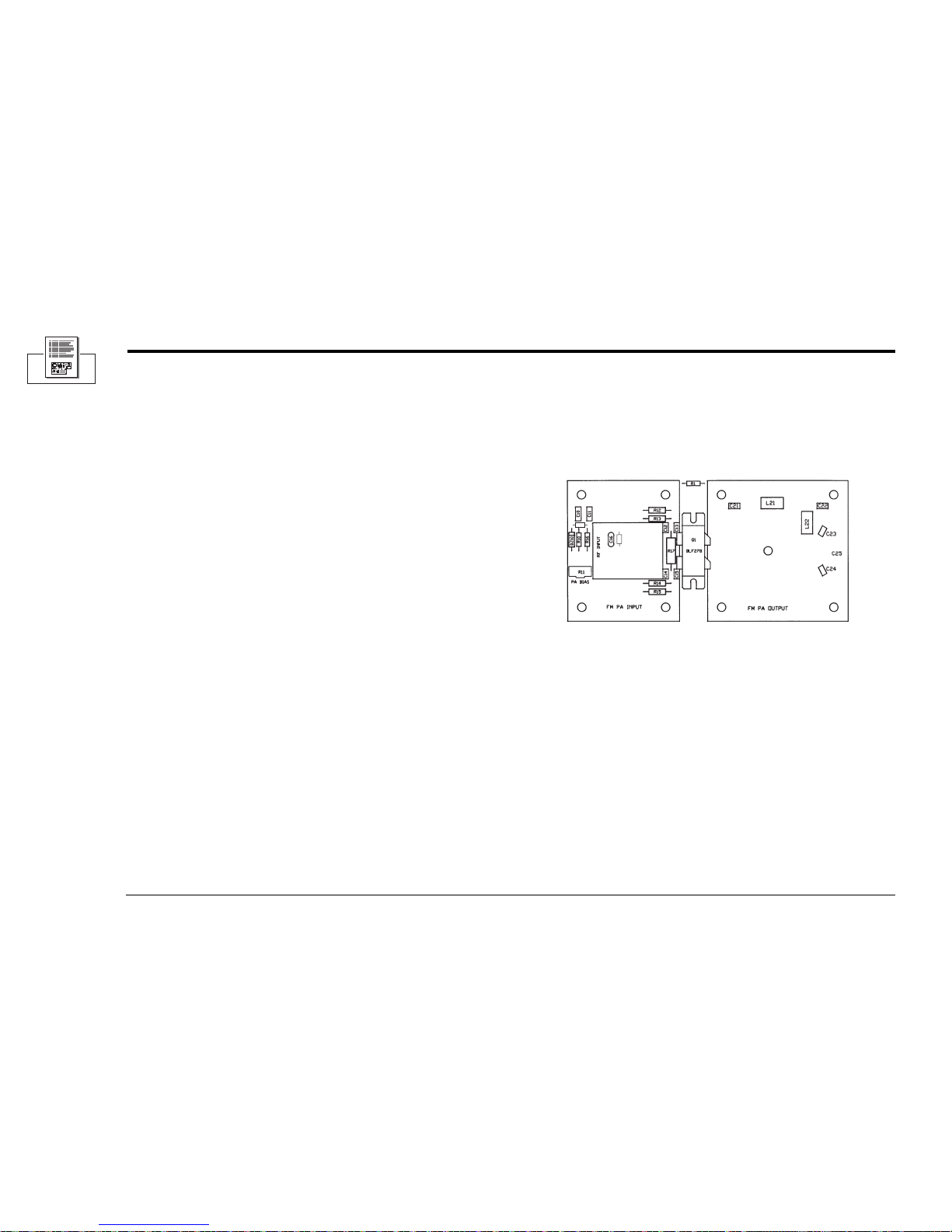
6–20
FM500 User's Manual
Illustration 6–13 Power Amplifier
(Add 1100 to component designators for schematic reference)
R20
R19
Page 86

6–21
Reference Drawings
FM500 POWER AMPLIFIER
J2
L902
R903
4.7K
C904
0.01
R904
51
T900
C900
0.01
R901
51
C901
0.01
R900
51
C903
0.01
U900
CA2832
L900
33uH
R902
2.7
5W
RF DRIVER BD
C908
27PF
C907
5PF
L904
23.2uH
C910
36PF
C906
36PF
L903
10.4uH
C905
10PF
C909
680PF
C902
0.01
D900
1N753A
6.2V
J3
DZ1110
1N4735
6.2V
R1119
200
3W
J5
R1120
2.7K
C1121
0.01
DISC
R1112
5.6
2W
R1113
5.6
2W
R1101
15K
C1126
0.1
R1110
10K
R1117
24
3W
C1138
0.068
C1112
0.01
C1113
0.01
C1114
0.01
C1115
0.01
R1116
10K
C1116
27PF
C1110
0.01
C1111
0.01
TEMP SENSE
C1122
0.01
DISC
L1122
50NH
L1121
50NH
C1125
60PF
C1123
0.01
C1124
0.01
123
LM35DZ
C1133
0.1
C1127
0.1
C1128
0.1
1
2
3
4
5
6
7
8
9
10
11
12
13
14
15
16
17
18
19
20
21
22
23
24
25
26
27
28
29
30
31
32
33
34
35
36
37
38
39
40
41
42
43
44
45
46
47
48
49
50
51
52
53
54
55
56
57
58
59
60
61
62
63
64
65
66
67
68
69
70
71
72
J1
C1137
0.1
C1136
0.1
C1132
0.1
C1134
0.1
C1135
0.1
+
_
B1
J2
C1131
0.1
C1130
0.1
PA OUTPUT BD
T1121
L1125A
L1125B
C1122
0.01
DISC
L1122
50NH
L1121
50NH
C1125
60PF
L1126
C1129
0.1
T11S
R1114
5.6
2W
R1115
5.6
2W
R1110
10K
R1120
2.7K
C1121
0.01
DISC
R1112
5.6
2W
R1113
5.6
2W
R1101
15K
R1117
24
3W
C1112
0.01
C1113
0.01
R1116
10K
C1110
0.01
C1111
0.01
PA INPUT BD
L1124A
L1124B
L1123
DZ1110
1N4735
6.2V
ZENER
R1119
200
3W
PA INPUT BD
R1114
5.6
2W
R1115
5.6
2W
C1116
27PF
C1114
0.01
C1115
0.01
C1138
0.068
PA OUTPUT BD
T1121
C1123
0.01
C1124
0.01
B3
B2
CROWN INTERNATIONAL, INC.
1718 WEST MISHAWAKA ROAD
DRAWN
CHECKED
SCALE
PROJ #
JFL
FILENAME: 1001771A.SCM
FM500 P.A.
ELKHART, IN. 46517 PHONE (219) 294-8000
DO NOT SCALE PRINT
SUPERSEDES
REV
ME
EE
PE
APPROVED BY :
NONE
DWG. NO.
E.C.
R103
NEXT ASM:
7-12-96
100177
A
THESE DRAWINGS AND SPECIFICATIONS ARE THE
SHALL NOT BE REPRODUCED, COPIED, OR USED
AS THE BASIS FOR THE MANUFACTURE OR SALE
OF APPARATUS OR DEVICES WITHOUT PERMISSION.
PROPERTY OF CROWN INTERNATIONAL, INC. AND
+
_
+
_
NOTES :
_______
_______
1. ALL RESISTORS ARE IN OHMS,
1/4W, 5% UNLESS OTHERWISE
SPECIFIED.
2. ALL CAPACITORS ARE IN
MICROFARADS UNLESS
OTHERWISE SPECIFIED.
9875321
Q1101
BLF278
Q1101
BLF278
T1111P
T11S
T1111P
R1111
10K
POT V
R1111
10K
POT V
R905 10K
R900
MRF 137
Page 87
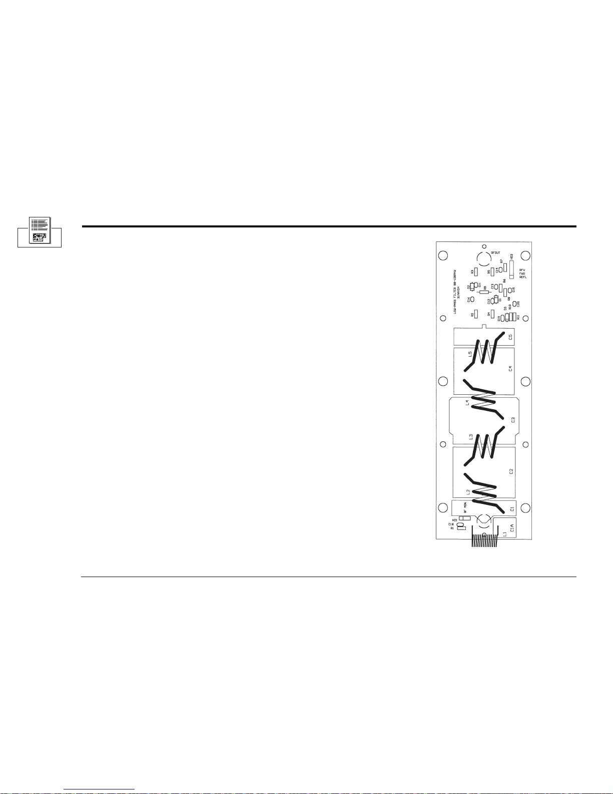
6–22
FM500 User's Manual
Illustration 6–14 RF Output Filter
(Add 1200 to component designators for schematic reference)
P10421-9
Page 88
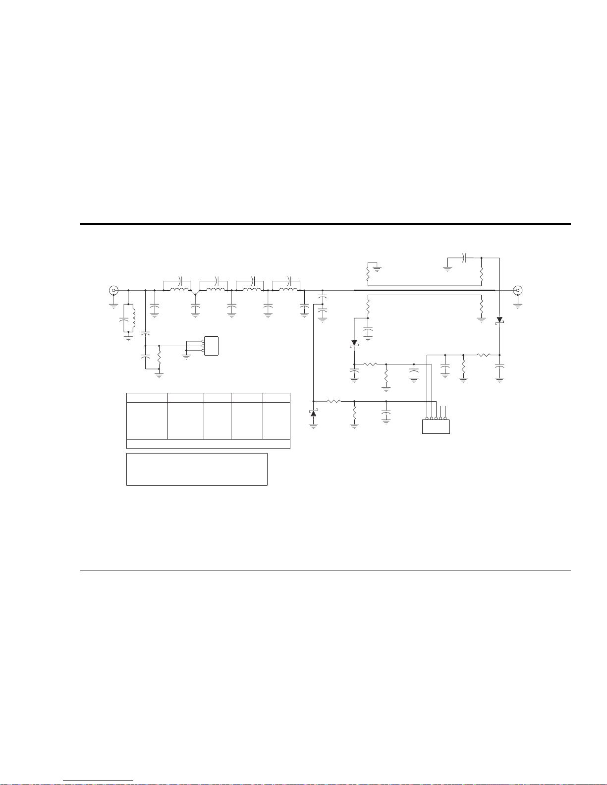
6–23
Reference Drawings
RF OUTPUT FILTER & REFLECTOMETER
103209
RF OUT
C1211
47PF NP0
R1203
10
*
R1202
75
C1204
7.1PF
C1206
9.3PF
C1208
5.13PF
L1203
94.1NH
L1204
87.5NH
(195MHz) (176MHz) (252MHz)
C1209A
2PF
L1205
77.9NH
RF IN
C1202
1.35PF
L1202
90.5NH
(455MHz)
C1201
15.4PF
C1203
40.9PF
L1201
250NH
C1201A
10PF
C1218
47PF SM
R1201
100
C1217
3.5PF
C1205
38.9PF
C1207
37.7PF
C1209
14.1PF
C1219
47PF SM
with 200W RF in.
Approx. 7V RMS
1
2
3
HD1201
RF MONITOR
F
W
D
R
E
F
L
C1212
47PF NP0
C1213
.001
C1215
.01
C1214
.01
D1201
1N6263
R1204
10
R1207
100K
R1206
1K
C1216
.001
*
D1202
1N6263
R1209
1K
R1205
75
R1208
20K
1 2 3 4 5
HD1202
HEADER 5
RFV
C1220
.01
R1210
10K
R1211
100K
14
3
3
3
3
LENGTH
0.7"
0.6"
GUAGE
#17
#12
#12
#12
#12
D1203
1N6263
0.6"
0.5"
0.7"
L1201
L1202
L1203
L1204
L1205
I.D. TURNS
0.25"
0.5"
0.5"
0.5"
0.4375"
INDUCTORS
*
50-OHM LOAD. R1205 = R1202
IF NECESSARY, SELECT R1202 FOR
SWR READING OF 1.1 OR BETTER WITH
R1202,R1203,C1211,D1202,C1216
ON UNDERSIDE OF CIRCUIT BOARD.
EXACT COIL LENGTHS ARE FACTORY-SET.
3. C1201-1209A,1217 are circuit board pads.
NOTES :
_______
_______
1. ALL RESISTORS ARE IN OHMS,
1/4W, 5% UNLESS OTHERWISE
SPECIFIED.
2. ALL CAPACITORS ARE IN
MICROFARADS UNLESS
OTHERWISE SPECIFIED.
Page 89
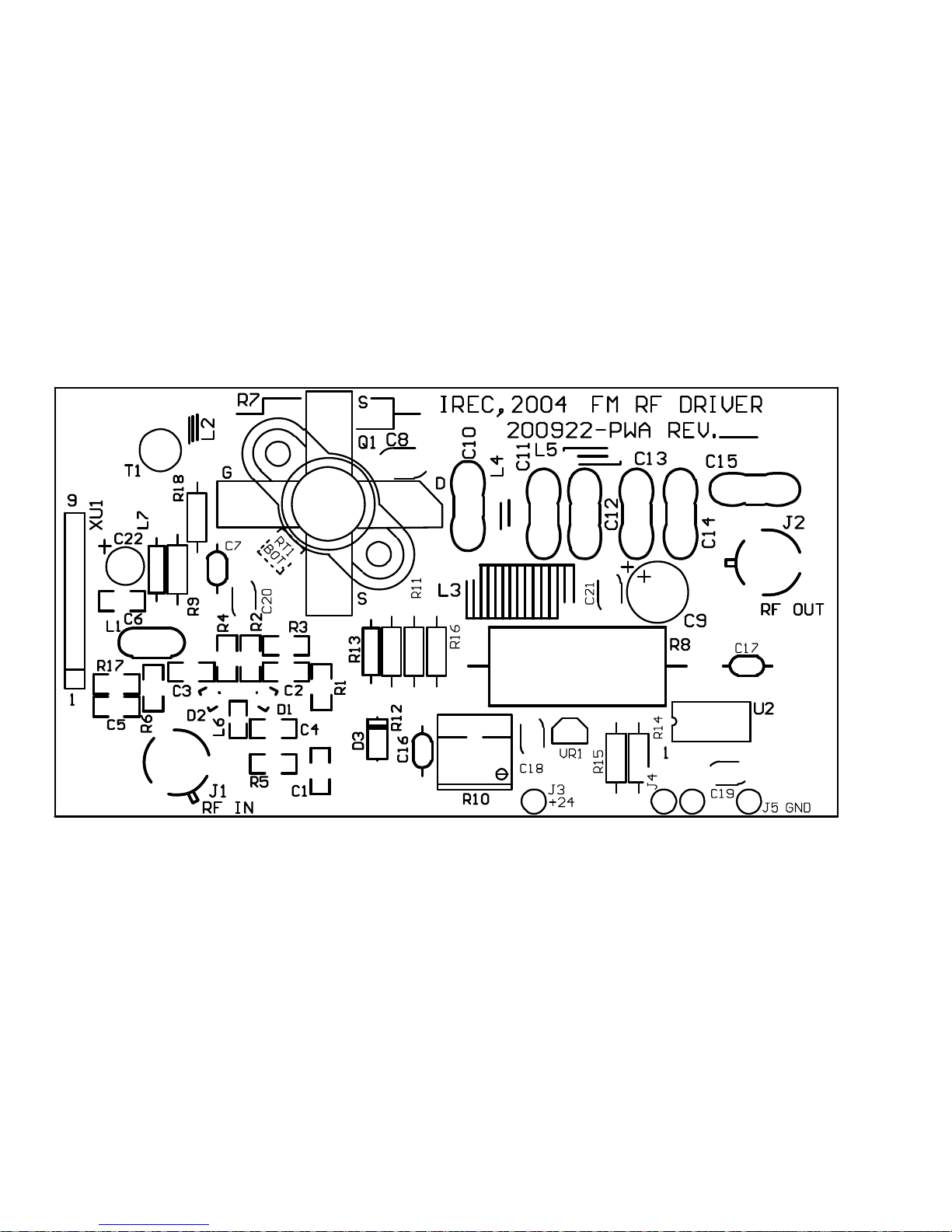
Page 90
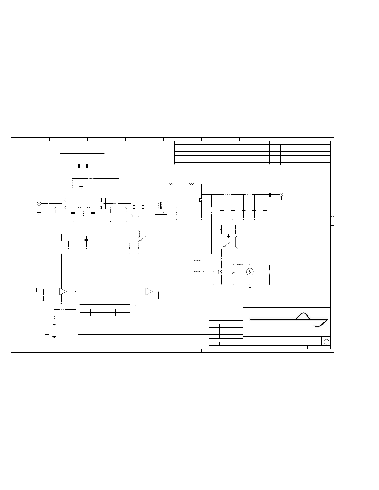
DWG. NO. REV.
Q43310-4
P
1 2 3 4 7 8
A
B
C
D
E
F
1 2 3 4 6 7 8
A
B
C
E
F
5
THESE DRAWINGS AND SPECIFICATIONS ARE THE PROPERTY OF
INTERNATIONAL RADIO AND ELECTRONICS CORP.
AND ARE NOT TO BE REPRODUCED, COPIED OR USED AS THE BASIS
FOR THE MANUFACTURE OR SALE OF APPARATUS OR
DEVICES WITHOUT PERMISSION.
1 1
SHEET
OF
SCALE : NONE
PROJ NO.
FILENAME:
DWG . NO .
REV.
P
Q43310-4
TITLE:
FM RF DRIVER
UNCONTROLLED
UNLESS OTHERWISE MARKED IN RED INK BY CM AS A
CONTROLLED COPY, COPIES OF THESE DOCUMENTS
INCLUDING ASSOCIATED ELECTRONIC REPRODUCTIONS
ARE FOR REFERENCE ONLY.
APPROVALS
DWN
CHK
CM
PE
DISTRIBUTION
E . C . N. REV DESCRIPTION
APPROVALS
PECHK CMDATE DWN
REVISION HISTORY
65
SIZE
B
B_L_SHT1_A.DOT REV. A
INTERNATIONAL RADIO AND ELECTRONICS CORP.
25166 LEER DRIVE ELKHART, IN. 46514
574-262-8900
WWW.IREC1.COM
IREC
L1
33uH
J1
RF IN
L2
OPEN
R10
10K
IN1GND2GND3N/C4VCC5N/C6GND7GND8OUT
9
XU1
MHW6342T
R1
OPEN
C6
0.01
C7
0.01
T1
Q1
BLF245
R2
OPEN
C15
680pF
L3
C10
10pF
C11
36pF
C12
36pF
C13
5pF
L4
10.4uH
L5
23.2uH
C14
27pF
J2
RF OUT
C9
OPEN
R11
4.7K
R9
51
C17
0.01
+24VDC
C16
0.01
C18
OPEN
1/2W
3
2
1
84
U2A
OPEN
5
6
7
U2B
OPEN
R15
OPEN
R14
OPEN
G
S
D
1
J3
1
J4
R13
OPEN
R12
OPEN
R8
*
D3
1N753A
6.2V
DW 08-28-03
533
1
J5
R7
OPEN
C8
OPEN
2
1
3
D1
OPEN
C1
.01
Vin
1
GND
2
Vout
3
VR1
OPEN
R16
OPEN
C2
OPEN
R4
OPEN
R3
OPEN
2
1
3
D2
OPEN
C3
.01
R6
OPEN
+5V
R5
OPEN
C4
OPEN
UNLESS OTHERWISE SPECIFIED:
NOTE:
1. ALL RESISTORS ARE IN OHMS, 1/4 WATT +/- 5% TOL.
2. ALL CAPACITORS ARE IN MICROFARADS.
L6
OPEN
R17
51
DW 10-30-03
DP 10-30-03
C19
OPEN
RT1
2.7K NTC
OPEN
T
L7
OPEN
C20
OPEN
C21
OPEN
C22
OPEN
R18
0
FM30 FM100 FM250 FM500
R8 POWER LEVEL CONFIGURATION
OPEN 3 OHM 5W 2.7 OHM 5W3 OHM 5W
FOR FM100 AND FM250: 18V
FOR FM500: 20V
FOR FM30: FEED POINT FROM PWR. REGULATOR PWB.
FOR FM30:
20VDC INPUT APPLIED HERE.
C5
22
C23
.01
C24
.01
ADDED TO PWB (200922-PWB-D IN LOCATION
SHOWN, AND DEPICTED ON COMPONENT MAP.
M PRODUCTION RELEASE 12-10-03
DW
DW DP264
N XU1 WAS 200479-TERM-10 01-29-04
DW
DW MH279
O PWB CHG'D TO REV. C 06-14-04
DW
DW DP316
P PWB CHG'D TO REV. D 03-22-05
DW
DW DP361
Page 91
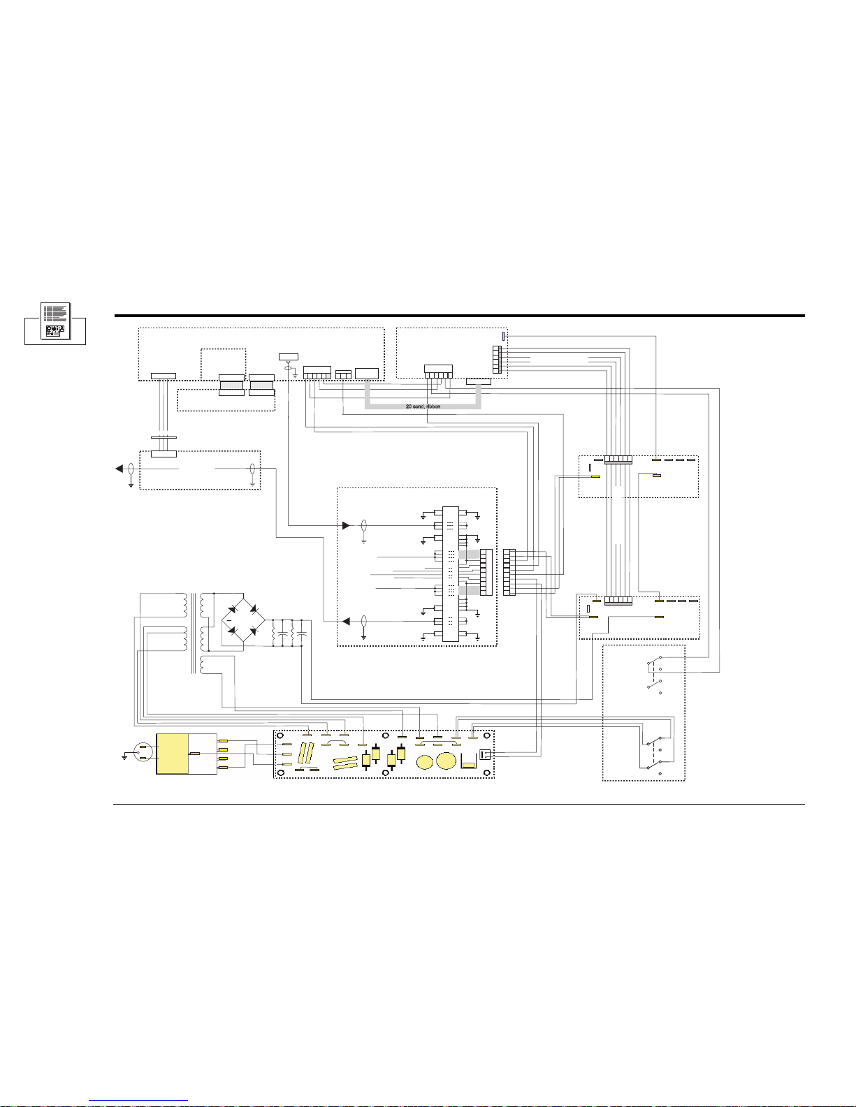
6–26
FM500 User's Manual
FM500 CHASSIS WIRING
FM500 Chassis Wiring
C.Donner 2-23-98
CROWN BROADCAST
AC Input, Fuse, & Filter
A
B
C
D
D
A
Gnd
Gnd
Red
Blk
Red/Wht
Brn/Wht
Brn
Wht
S1A S1B
P1
100V
220V
120V
240V
P7 P6
P5 P4
Blk/Wht
P801
P802
P803
P804
P806
P805
P807
P808
Right Power
Regulator Board
P801
P802
P803
P804
P806
P805
P807
P808
Red
Blk
Fan
1
2
3
4
6
7
8
9
10
1
2
3
4
5
6
HD701
P1
Unreg
Carrier
Switch
V+
Gnd
Power Transformer
RED / WHT
RED
WHT / BLK
WHT
BLK
BRN
BRN / WHT
BLU / WHT
BLU
1
3
4
5
6
2
1
2
3
4
5
6
1
2
3
4
5
6
P3
Ribbon Cable
+
Bridge
Rectifier
AC
Power
Switch
Ribbon Cable
On
Off
1
2
4
5
6
8
9
12
13
14
15
17
18
20
19
22
23
24
25
28
29
31
32
33
35
36
Driver input
BNC
PA 1 DC Input
PA RF Output
BNC
37
38
40
41
42
44
45
46
47
54
55
56
57
52
53
62
63
64
65
67
68
69
71
72
PA 2 DC Input
P1
P2
Outer Fans
Inner Fan
Driver DC Input
Mother Board
Voltage Regulator
Board
1
3
1
2
3
4
5
6
1
2
3
4
6
7
8
9
10
Header Socket
Power Amp Interconnect
Board
J1
Bus
Bus
DC
DC
AC Distribution Board
Temp Sensor
Back view
*
*
*
*
Jumpered for 120VAC
On
Off
Display Board
HD561
J 601
J 602
Metering
Board
J 403
Ribbon Ribbon
HD504
HD1202
RF Output
Filter & Reflectometer Board
RF Out
RF In
HD505
Reflectometer Feed-Thru
P3
55
HD 502
HD503
2
Temp
HD702
Left Power
Regulator Board
120 VAC
20 VAC
100 VAC
57 VAC
57 VAC
12.5 VAC
CHASSIS WIRING
Page 92
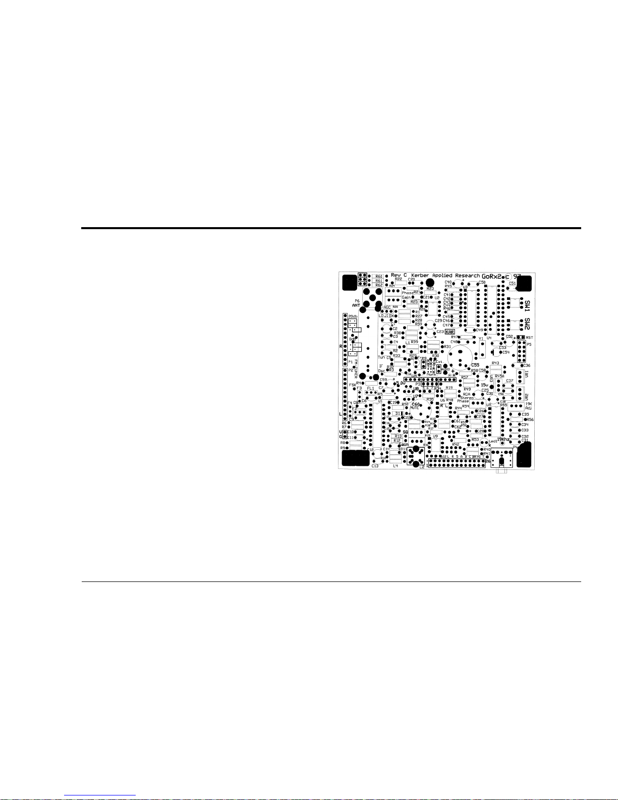
6–27
Reference Drawings
Illustration 6–16 Receiver Board
Page 93
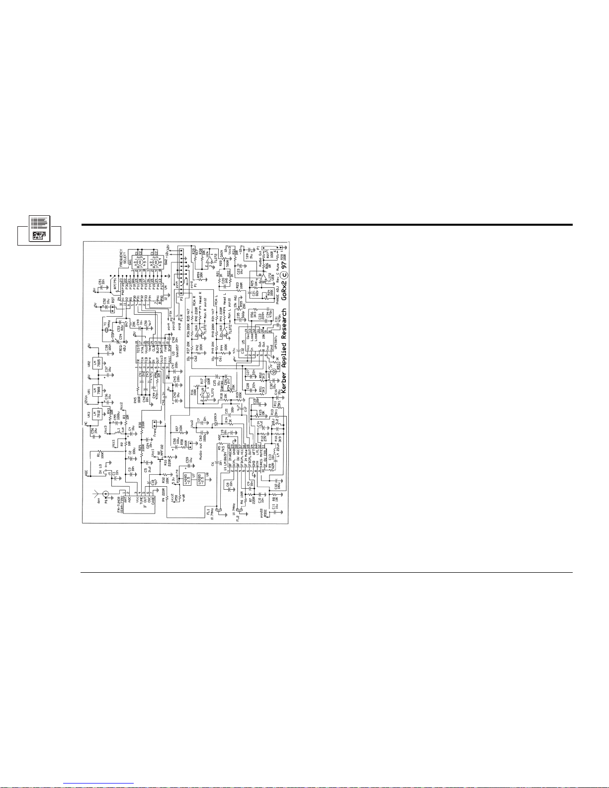
6–28
FM500 User's Manual
Receiver
Page 94
Section 7—Service and Support
We understand that you may need various levels of support or
that the product could require servicing at some point in time.
This section provides information for both of these scenarios.
Service and Support
7–1
Page 95

7.1 Service
The product warranty (see opposite page) outlines our responsibility for defective
products. Before returning a product for repair or replacement (our choice), call
our Customer Service department using the following telephone number:
(866) 262-8917
Our Customer Service Representative will give you further instructions regarding
the return of your product. Use the original shipping carton or a new one obtained
from Crown. Place shipping spacers between the slide-out power amplifier assembly and the back panel.
Please fill out the Factory Service Instructions sheet (page 7–5) and include it with
your returned product.
7.2 24–Hour Support
In most instances, what you need to know about your product can be found in this
manual. There are times when you may need more in-depth information or even
emergency-type information. We provide 24–hour technical assistance on your
product via a toll telephone call.
For emergency help or detailed technical assistance, call
(866) 262-8917
You may be required to leave a message at this number but your call will be
returned promptly from our on-call technician.
7.3 Spare Parts
To obtain spare parts, call Crown Broadcast Sales at the following number.
(866) 262-8917
You may also write to the following address:
Service Manger
International Radio and Electronics Company, Inc.
25166 Leer Drive
Elkhart, Indiana, U.S.A. 46514-5425
7–2
FM500 User's Manual
Page 96

Three-Year Limited Warranty
North America Only
SUMMARY OF WARRANTY
We, Crown Broadcast, a business unit of International Radio and Electronics Company, Inc., 25166 Leer
Drive, Elkhart, Indiana 46515–2000 warrant to the ORIGINAL PURCHASER of a NEW Crown Broadcast
product, for a period of three (3) years from the date of purchase by the original purchaser (the “warranty
period”) that the new Crown Broadcast product is free of defects in materials and workmanship and will
meet or exceed all advertised specifications for such a product. This warranty does not extend to any
subsequent purchaser or user, and automatically terminates upon sale or other disposition of our
product.
ITEMS EXCLUDED FROM THIS CROWN BROADCAST
We are not responsible for product failure caused by misuse, accident, or neglect. This warranty does not
extend to any product on which the serial number has been defaced, altered, or removed. It does not cover
damage to loads or any other products or accessories resulting from Crown Broadcast product failure. It
does not cover defects or damage caused by use of unauthorized modifications, accessories, parts, or
service.
WHAT WE WILL DO
We will remedy any defect, in material or workmanship (except as excluded), in our sole discretion, by
repair, replacement, or refund. If a refund is elected, then you must make the defective or malfunctioning
component available to us free and clear of all liens or other encumbrances. The refund will be equal to
the actual purchase price, not including interest, insurance, closing costs, and other finance charges less
a reasonable depreciation on the product from the date of original purchase. Warranty work can only be
performed at our authorized service centers or at our factory. Expenses in remedying the defect will be
borne by Crown Broadcast, including two-way surface freight shipping costs within the United States.
(Purchaser must bear the expense of shipping the product between any foreign country and the port of
entry in the United States and all taxes, duties, and other custom’s fee(s) for such foreign shipments.)
HOW TO OBTAIN WARRANTY SERVICE
You must notify us of your need for warranty service not later than ninety (90) days after the expiration
of the warranty period. We will give you an authorization to return the product for service. All components
must be shipped in a factory pack or equivalent which, if needed, may be obtained from us for a nominal
charge. Corrective actions will be taken within a reasonable time of the date of receipt of the defective
product by us. If the repairs made by us are not satisfactory, notify us immediately.
DISCLAIMER OF CONSEQUENTIAL AND INCIDENTAL DAMAGES
You are not entitled to recover from us any consequential or incidental damages resulting from any defect
in our product. This includes any damage to another product or products resulting from such a defect.
WARRANTY ALTERATIONS
No person has the authority to enlarge, amend, or modify this warranty. The warranty is not extended by
the length of time for which you are deprived of the use of the product. Repairs and replacement parts
are provided under the terms of this warranty shall carry only the unexpired portion of this warranty.
DESIGN CHANGES
We reserve the right to change the design of any product from time to time without notice and with no
obligation to make corresponding changes in products previously manufactured.
LEGAL REMEDIES OF PURCHASER
There is no warranty which extends beyond the terms hereof. This written warranty is given in lieu of any
oral or implied warranties not contained herein. We disclaim all implied warranties, including without
limitation any warranties of merchantability or fitness for a particular purpose. No action to enforce this
warranty shall be commenced later than ninety (90) days after expiration of the warranty period.
Crown Broadcast, International and Radio Company, Inc.
25166 Leer Drive, P.O. Box 2000, Elkhart, Indiana 46515–2000
Service and Support
Revised August 2001
7–3
Page 97

Notes:
7–4
FM500 User's Manual
Page 98

Factory Ser vice Instructions
To obtain factory service, complete the bottom half of this page, include it with the unit, and ship to:
International Radio and Electronics Company, Inc.
25166 Leer Drive
Elkhart, Indiana, U.S.A. 46514-5425
For units in warranty (within 3 years of purchase from any authorized Crown Dealer): We pay for
ground UPS shipments from anywhere in the continental U.S. and Federal Express Second Day service
from Hawaii and Alaska to the factory and back to you. Expedited service/shipment is available for an
additional charge. You may ship freight collect (COD for cost of freight) or forward your receipt for
shipping charges which we will reimburse. We do not cover any charges for shipping outside the U.S.
or any of the expenses involved in clearing customs.
If you have any questions about your Crown Broadcast product, please contact Crown Broadcast
Customer Service at:
Telecphon: (574) 262-8900
Fax: (574) 262-5399
Name: Company:
Shipping Address:
Phone Number: Fax:
Model: Serial Number: Purchase Date:
Nature of the Problem
(Describe the conditions that existed when the problem occurred and what attempts were made to correct it.)
Other equipment in your system:
If warranty has expired, payment will be: Cash/Check VISA Mastercard COD
Please Quote before servicing
Card Number: Exp. Date: Signature:
Service and Support
7–5
Page 99

Appendix
Transmitter Output Efficiency
FM500 User's Manual
Appendix–1
Page 100

T ransmitter efficiency output
RF Power Output Efficiency-FM500
PADC V olts PADC Amps RF Power Efficiency
51.3 13.91 550 77%
48.3 13.29 500 78%
45.5 12.74 450 77%
42.7 12.14 400 77%
39.4 11.46 350 78%
36.0 10.68 300 78%
33.0 10.00 250 76%
29.6 9.25 200 73%
25.4 8.28 150 71%
21.1 7.29 100 6 5 %
Power measurements were made at 97.1 MHz. Voltage and current
measurements were taken from the unit's built-in metering. The accuracy of
the internal metering is better than 2%. Return loss of the RF load was greater
than -34dB at test frequency.
Appendix–2
FM500 User's Manual
 Loading...