

FX806A
A
UDIO PROCESSOR
SERIAL
CLOCK
MAIN
PROCESS
OUT
XTAL/CLOCK
CLOCK
GENERATOR
DE-EMPHASIS
FILTER
(RX)
AUDIO IN
INPUT
PROCESS
MAIN PROCESS
OUTPUT DRIVES
To EXTERNAL AUDIO
PROCESSES
EXTERNAL AUDIO
PROCESS IN
CALIBRATION INPUT
ATTENUATOR
CHIP
SELECT
PRIMARY
and
SECONDARY
AUDIO
INPUTS
———
Voice.
Sub-/Audio
Tone.
FFSK.
etc.
SUM
OUT
MOD.
IN
COMMAND
DATA
#
# #
(TX)
MIC. IN
ATTENUATOR
MODULATION 2
OUT
MODULATION 1
OUT
LOUDSPEAKER
AUDIO
TRANSMITTER
MODULATION
DRIVES
C-BUS INTERFACE
VOGAD SENSE
ATTENUATOR
MODULATION
SUMMING
AMP
POWER
SUPPLY
PRE-EMPHASIS
LIMITING
FILTERING
GAIN SETTING
# indicates logic control
#
#
#
# # #
#
#
#
MIC. & VOGAD
AMPS
LOW &
HIGHPASS
FILTERS
GAIN
SET
VOGAD
SENSE
#
#
BUFFER
VOGAD
SENSE
XTAL
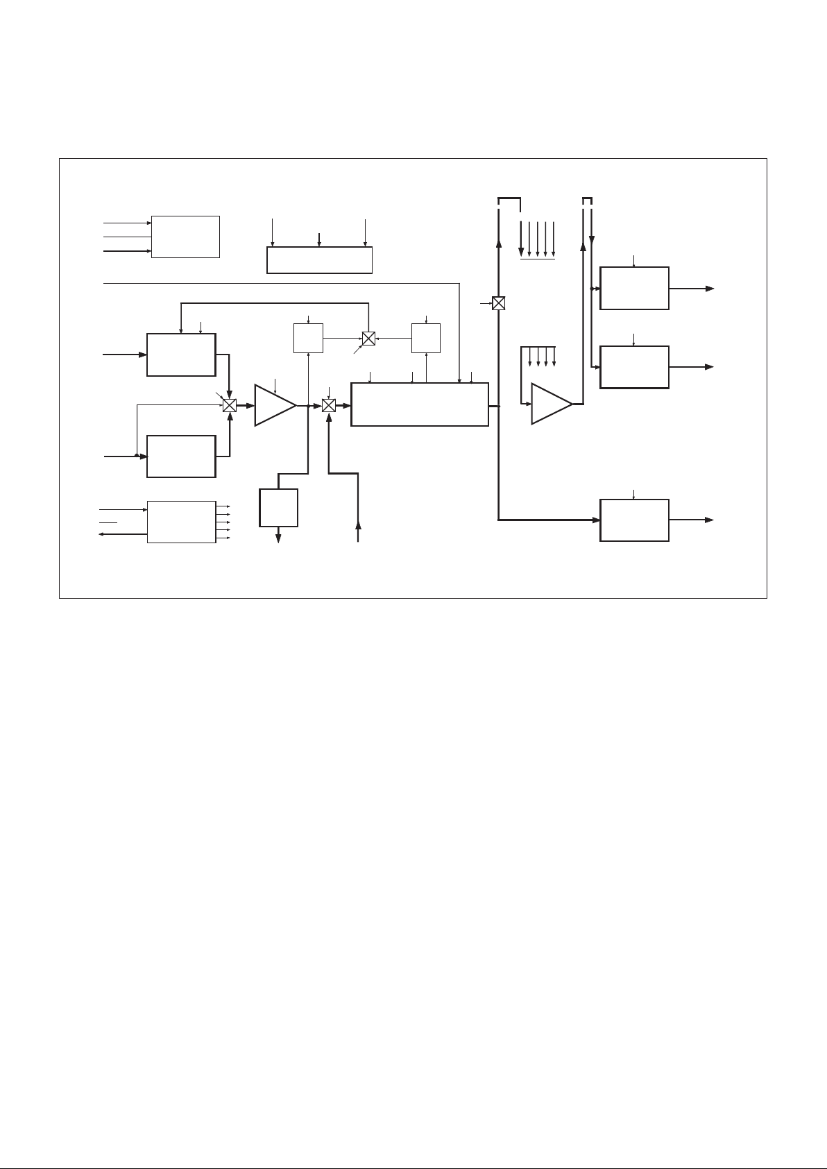
Fig.1 FX806A Audio Processor
● Main Process
Conditioning for Input or External Process signals with
gain/pre-emphasis, high and lowpass switched capacitor
filters and a transmitter deviation limiter. The Main Process
Output may be switched to V
BIAS
.
● Summation and Output Drives
Main “voice audio” from the Main Process is combined
with signalling and data from other DBS 800 facilities, to
provide the composite (in and outband) signal for the digitally
adjustable Transmitter Modulation Drives.
Received audio is level (volume) adjusted for output to
loudspeaker circuitry.
Signal-level stability and therefore output accuracy, of
the FX806A is maintained by a voltage-controlled gain
system (VOGAD) with specific gain sensors that are selected
automatically by the Internal/External Mode Command. The
VOGAD system permits high deviation with low distortion.
This is achieved by reducing the path gain (and so reducing
the distortion introduced by the Peak Deviation limiter) when
the input signal is large.
Signal levels can be controlled to provide ‘dynamiccompensation’ for such factors as temperature drift, VCO
non-linearity, etc.
FX806A audio output stages can be completely disabled
or the whole microcircuit placed into a “Powersave” mode,
leaving only clock and “C-BUS” circuitry active.
The FX806A is a low-power, 5-volt CMOS integrated
circuit and is available in 24-pin DIL cerdip and 24-pin/lead
plastic SMD packages.
Brief Description
Intended primarily to operate as the “Audio Terminal” of
Radio Systems using the DBS 800 Digitally-integrated
Baseband System, the FX806A is a PMR Audio Processor
which meets EIA and CEPT audio specifications.
Using a unique filter line-up, the FX806A offers lower
distortion versus modulation level figures than conventional
filter/limiter configurations.
The FX806A is a half-duplex device whose signal paths
and level-setting elements are dynamically configured and
adjusted by digital information sent from the Radio
µController using “C-BUS” hardware and software protocol.
Figure 5 shows a complete functional block diagram of
the FX806A signal paths which can be viewed as 3 sections:
● Input Process
Selectable transmit or receive input paths.
The transmit path with low-noise input and VOGAD
amplifiers and bandpass filtered stages provides good signalto-noise performance at low input levels and minimum
distortion for high-drive modulation signals.
De-emphasis is software selectable at the Rx Audio Input
for FM or PM radio configurations.
This initial audio, after in-line gain adjustment, is
available for switching to either external audio processes
(such as scrambling) or internally to the Main Process
stages.
Publication D/806A/3 July 1994
2
Pin Number Function
FX806A
J/LG/LS
1
2
3
4
5
6
7
8
9
10
11
12
Xtal: The output of the on-chip clock oscillator. External components are required at this output when
a Xtal circuit is employed. See Figure 2, INSET 2.
Xtal/clock: The input to the on-chip clock oscillator inverter. A Xtal or externally derived clock should
be connected here. See Figure 2, INSET 2. This clock provides timing for on-chip elements, filters etc.
Serial Clock: The “C-BUS,” serial data loading clock input. This clock, produced by the µController, is
used for transfer timing of Command Data to the Audio Processor. See Timing diagrams and System
Support Document.
Command Data: The “C-BUS,” serial data input from the µController. Command Data is loaded to
this device in 8-bit bytes, MSB (B7) first, and LSB (B0) last, synchronized to the Serial Clock. The
Command/Data instruction is acted upon at the end of loading the whole instruction. Command
information is detailed in Tables 1, 2, 3, 4 and 5. See Timing diagrams and System Support
Document.
Chip Select (CS): The “C-BUS,” data loading control function. This input is provided by the
µController. Command Data transfer sequences are initiated, completed or aborted by the CS signal.
See Timing diagrams and System Support Document.
VOGAD Out: The output of the relevant VOGAD sensor. This output, with external attack and decay
setting components, should be connected as in Figures 2 and 3, to the VOGAD In pin.
Rx Audio In: The audio input to the FX806A from the radio receiver's demodulator circuits. This
input, which requires to be a.c. coupled with capacitor C
12
, is selected by a Control Command bit.
VOGAD In: The gain control signal from the selected VOGAD sensor (VOGAD Out) to the “Input
Process” Voltage Controlled Amplifier. VOGAD operation is enabled via a Mode Command (Bit5).
Individual sensors, automatically selected, permit gain control from either the Input Process or an
external process. External attack and decay setting components should be applied as recommended
in Figures 2 and 3.
V
BIAS
: The output of the on-chip analogue circuitry bias system, held internally at VDD/2. This pin
should be decoupled to VSS by a capacitor C10, See Figure 2.
Mic In (+): The non-inverting input to the microphone Op-Amp. This input requires external
components for Op-Amp gain/attenuation setting as shown in Figure 2, INSET 1.
Mic In (–): The inverting input to the microphone Op-Amp. This input requires external components
for Op-Amp gain/attenuation setting as shown in Figure 2, INSET 1.
V
SS
: Negative supply rail (GND).

3
Pin Number Function
FX806A
J/LG/LS
13
14
15
16
17
18
19
20
21
22
23
24
Mic Out: The output of the microphone Op-Amp, used with the Mic In (–) input to provide the required
gain/attenuation using external components as shown in Figure 2. The external components shown are
to assist in the use of this amplifier with either inverting or non-inverting inputs. During Powersave
(Volume Command) this output is placed at V
SS
.
Processed Audio In: The input to the device from such external audio processes as Voice Store and
Retrieve or Frequency Domain Scrambling. This input, which requires to be a.c. coupled with a
capacitor, C
13
, is selected by a Mode Command bit.
External Audio Process: The buffered output of the Input Processing stage. For further external
audio processing prior to re-introduction at the Processed Audio In pin.
CALibration Input: A unique input, intended to be used for dynamic balancing of the modulator drives
and for measuring Deviation Limiter levels. A CUE (beep) input from the FX803 Audio Tone Processor
can be entered on this line. This input is selected via a Mode Command bit (11
H
) and is self-biased.
Main Process Out: The output of the Main Process stage. This output is summed with additional
system inputs as required (Audio, Sub-Audio Signalling, FFSK – See System Overview) in the on-chip
Modulation Summing Amplifier. External components as shown in Figure 2 should be used as required.
Sum In:
The input and output terminals of the on-chip Modulation Summing Amplifier. External components
are required for input signals, with gain/attenuation setting as shown in Figure 2. For single-signal,
no-gain requirements, Main Process Out may be linked directly to Modulation In.
Sum Out:
Modulation In: The final, composite modulating signal to VCO (Mod 1) and Reference (Mod 2) Output
Drives.
Audio Output: The processed audio signal output intended as a received audio (volume) output.
Though normally used in the Rx mode, operation in Tx is permitted. The output level of this attenuator is
controlled via a Volume Set command. During Powersave this output is placed at V
SS
.
Modulation 1 Drive: The drive to the radio modulator Voltage Controlled Oscillator (VCO), from the
composite audio summing stage.
Modulation 2 Drive: The drive to the radio modulator Reference Oscillator, from the composite audio
summing stage.
NOTE: These VCO output attenuators are individually adjustable using the Modulator Levels command.
During Powersave these outputs are placed at V
SS
.
V
DD
: Positive supply rail. A single, stable +5 volt supply is required. Levels and voltages within the
Audio Processor are dependant upon this supply.
4
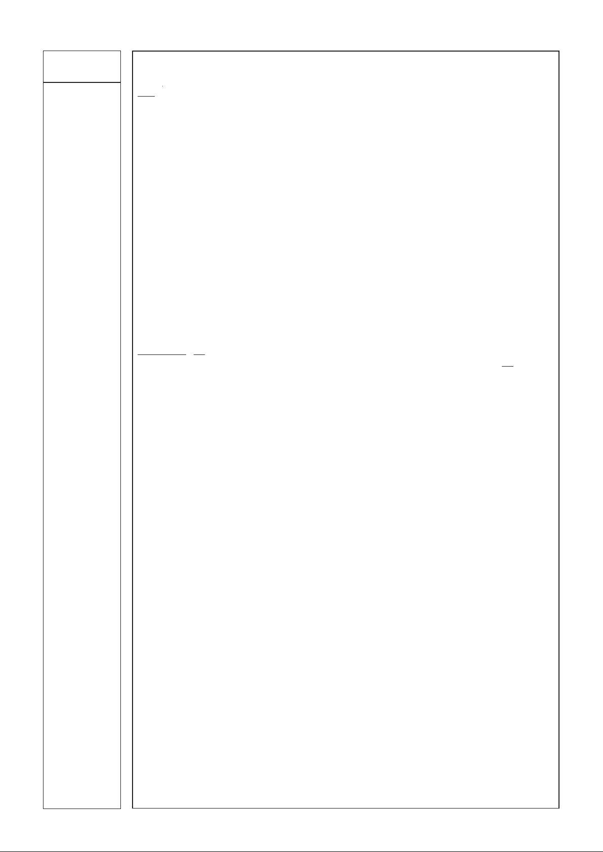
Analogue Application Information
External Components
MAIN
PROCESSOUT
XTAL/CLOCK
C
9
VOGAD OUT
VOGAD IN
MIC. IN (+)
MIC. IN (-)
SERIAL CLOCK
COMMAND DATA
CHIP SELECT
RX AUDIO IN
MIC. OUT
PROCESSED AUDIO IN
EXTERNAL AUDIO PROCESS
CALIBRATION IN
SUM IN
SUM OUT
MOD IN
AUDIO OUT
MODULATION 1 DRIVE
MODULATION 2 DRIVE
EXTERNAL SIGNAL
AND
DATA INPUTS
C
8
C
10
R
5
C
12
SEE INSET 2
SEE INSET 1
R
8
R
7
R
9
R
10
C
13
INSET 2
XTAL/CLOCK
C
7
X
1
1
2
FX806A J
INSET 1
MIC. IN (+)
MIC. IN (-)
MIC. OUT
10
11
13
+
-
R
3
C
3
C
1
R
1
C
2
R
2
C
4
C
5
R
4
FX806A J
XTAL
R
12
V
SS
V
DD
XTAL
V
BIAS
V
SS
V
SS
R
11
V
SS
V
SS
C
6
V
BIAS
C
11
V
DD
13
14
15
16
17
18
19
20
21
22
23
24
1
2
3
4
5
6
7
8
9
10
11
12
FX806A J
R
6
Fig.2 Recommended External Components
Component Value
R
1
= 10.0kΩ
R
2
10.0kΩ
R
3
20.0kΩ
R
4
20.0kΩ
R
5
10.0kΩ
R
6
2.2MΩ
R
7
100kΩ
R
8
100kΩ
R
9
100kΩ
R
10
= 100kΩ
R
11
100kΩ
R
12
2.2MΩ
C
1
470nF
C
2
470nF
C
3
270pF
C
4
270pF
C
5
0.1µF
C
6
33pF
C
7
= 5 – 65pF
C
8
1.0µF
C
9
1.0µF
C
10
1.0µF
C
11
22pF
C
12
100nF
C
13
10.0nF
X
13
4.0MHz
Tolerance: R = ±10%. C = ± 20%
Notes
To demonstrate the versatility of the Mic. inputs, Input
Op-Amp gain/attenuation components for a voltage gain of
6.0dB are shown (INSET 1) in a differential configuration.
Components for a single (+ or -) input may be employed.
Resistor values R7 to R11 (summation components) are
dependant upon application and configuration requirements.
Xtal circuit capacitors C6 (CD) and C7 (CG) shown (INSET
2) are recommended in accordance with
CML Application
Note D/XT/2 December 1991
. Circuit drive and drain resistors
are incorporated on-chip.
Operation of any CML microcircuit without a Xtal or clock
input may cause device damage. To minimise damage in the
event of a Xtal/drive failure, it is recommended that the power
rail (VDD) is fitted with a current limiting device (resistor or fast
reaction fuse).
VOGAD Components Calculations – Figures 2 and 3
Provided R
5
>>1.0kΩ and R6 = R12 >>R
5
Then:
Attack Time (TA) = R5 x C
8
Decay Time (TD) = R6 x C
8
2

5
Analogue Application Information ......
VOGAD
IN
MIC. IN
MIC. IN
VOLTAGE
CONTROLLED (VOGAD)
AMPLIFIER
PROCESSED AUDIO IN
Tx INPUT PROCESS
To EXTERNAL AUDIO PROCESSES
5
R
6
R
12
R
8
C
EXTERNAL INTEGRATION COMPONENTS
MIC. OUT
MAIN PROCESS
CAL INPUT
VOGAD
OUT
Tx
DRIVES
Rx
DRIVE
SS
V
DD
V
HI/LO
PEAK DETECTOR
Tx
HI
PEAK
DETECTOR
The Gain Control System
Tx Calibration :
From Mic. In to Modulator Drives Out
Disable Peak Detectors (Mode Command).
Set Transmitter Drives to 0dB (Mod Levels Set).
Pre-emphasis may be employed as required (Control
Command).
Set Input Level Amp to 0dB (Control Command).
(1) Mic. In = 250mVrms at 1kHz; Set Process Gain Amp for
output of 1440mV p - p (100% deviation).
(2) With Process Gain Amp set as (1); Mic In = 25mVrms at
1kHz, set Input Level Amp for output level of 308 mVrms
(60% deviation).
Rx Calibration:
From Rx Audio In to Audio Output
Set Audio Output Drive to 0dB (Volume Set).
Leave Process Gain Amp set as In (1) (above).
(3) With Rx Audio In level of between 154mVrms and
308mVrms (see Specification page), at 1kHz, set the
Input Level Amp for an output level of 308mVrms.
Fig.3 “VOGAD” Sensors and Timing Components – (part of Fig.4)
Tx gain control of the FX806A is by 1 of 2 selectable signal
peak detectors whose output is fed via external integrating
components to the Voltage Controlled Amplifier positioned
in the Tx Input Process Path.
The integrated level to the VOGAD In pin causes the Voltage
Controlled Amplifier gain to be reduced. VOGAD attack
and decay calculations are described at the foot of the
proceeding page.
The FX806A automatically chooses the appropriate peak
detector when the signal path is set by a Mode Command.
The Hi/Lo Peak Detector is employed when external audio
processes are used.
The Hi Peak Detector is employed when external audio
processes are not used.
Suggested Calibration Methods
To effectively null all internal microcircuit tolerances, the following initial calibration routine is suggested:
Fig.4 Distortion vs Mic. Input Level
0.2 0.4 0.6
Mic. Input Level (Vp-p)
Output Distortion (%)
Limiter Only
“Hi-Peak” VOGAD & Limiter
0.0
0
5
10
15
20
25
+10.0
0.0
+20.0
Input Level (dB)
60%
Output Deviation
308mVrms
0.071
Internal Path with Pre-emphasis
Circuit Elements set to 0dB
Input Level for 0dB = 71.0mV p-p
Input Frequency = 1.0kHz
Output Deviation = 60% = 0dB

6
PLMR Audio Processor Explanatory Block Diagram
Fig.5 PLMR Audio Processor – Facilities
NOTES
MAIN PROCESS
DEVIATION
LIMITER
PROCESS
GAIN
AMP
MODULATION
SUMMING
AMPLIFIER
OUTPUT DRIVES
CALIBRATION INPUT
EXTERNAL AUDIO
PROCESS
XTAL/CLOCK
SERIAL CLOCK
COMMAND DATA
PROCESS
L.P.F.
PROCESS
L.P.F.
+3dB to -4dB
VOGAD
OUT
VOGAD
IN
EXTERNAL
SIGNAL/DATA
INPUTS
MAIN PROCESS
OUT
SUM
IN
SUM
OUT
MODULATION
IN
TRANSMITTER
MODULATOR
DRIVES
MIC. IN
MIC. IN
INPUT PROCESS
INPUT
LEVEL
AMP
DE-EMPHASIS
MIC.
OP-AMP
MIC. OUT
INPUT
H.P.F.
Tx
Rx
+10dB to -4dB
Rx (DEMOD) AUDIO IN
PROCESSED AUDIO IN
V
DD
V
SS
#C0 - 3
Tx
Rx
#M0 - 2
# = Controlling Logic Bit
C = Control Command
M = Mode Command
0dB Level = 308mVrms (60% Deviation)
.
D0 = Mod 2
D1 = Mod 1
V = Volume Set
INPUT SELECT
#C6 (ENABLE)
EXTERNAL SIGNAL MIXING
EXTERNAL INTEGRATION
COMPONENTS
XTAL
Tx
0dB to -12.4dB
MOD
1
dB dB
#D(1) 0-4
dB dB
0dB to -6.2dB
#D(0) 0-4
AUDIO
OUTPUT
0dB to -48.0dB
dB
dB
#V0 - 4
#C7 (ENABLE)
MOD
2
0dB
0dB
0dB @ 1kHz
Gain Set By
External Components
#
BUFFER
AMP
C-BUS INTERFACE
AND
CONTROL LOGIC
#
#
VOGAD
AMP
0dB
INPUT
L.P.F.
0dB
-6dB/oct
H.P.F.
V
BIAS
+6dB/oct
0dB
0dB
V
BIAS
CLOCK
GENERATOR
CHIP SELECT
-24dB
to
6dB
V
BIAS
#C4
#M4
V
BIAS
V
BIAS
V
BIAS
#M6
ON OFF
#M3
#C5
#M7
#M3
HI-PEAK
DETECTOR
+VE PEAKS
HI/LO-PEAK
DETECTOR
+VE & -VE PEAKS
#V6
0dB
PRE-EMPHASIS
10dB @ 1kHz
0dB
H.P.F.
0dB

7
Controlling Protocol
Control of the functions and levels within the FX806A PLMR Audio Processor is by a group of Address/Commands and
appended data instructions from the system µController to set/adjust the functions and elements of the FX806A. The use of
these instructions is detailed in the following paragraphs and tables.
Control Bits
Transmitted First
Audio Output (Rx)
Disabled
Enabled
Modulation Drives
Disabled
Enabled
Pre-Emphasis
By-Pass
Enabled
Input Select
Rx Audio In
Mic. In
Input Level Set
Input Amp Disabled
-4.0dB
-3.0dB
-2.0dB
-1.0dB
0dB
1.0dB
2.0dB
3.0dB
4.0dB
5.0dB
6.0dB
7.0dB
8.0dB
9.0dB
10.0dB
Setting
MSB
Bit 7
0
1
6
0
1
5
0
1
4
0
1
32 10
00 00
00 01
00 10
00 11
01 00
01 01
01 10
01 11
10 00
10 01
10 10
10 11
11 00
11 01
11 10
11 11
Mode Bits
Transmitted First
Drive Source
Signals
Calibration
Deviation Limiter
Disabled
Enabled
VOGAD
Disabled
Enabled
De-Emphasis
Enabled
By-Passed
Signal Select
Internal
External
Process Gain Set
-4.0dB
-3.0dB
-2.0dB
1.0dB
0dB
1.0dB
2.0dB
3.0dB
Setting
MSB
Bit 7
0
1
6
0
1
5
0
1
4
0
1
3
0
1
210
000
001
010
011
100
101
110
111
Control Command
(Preceded by A/C 10H)
Table 2 Control Commands
Table 3 Mode Commands
Mode Command
(Preceded by A/C 11H)
Command Address/Command (A/C) Byte Command Table
Assignment Hex Binary Data
MSB LSB
General Reset 01 0 0 0 0 0001
Control Command 10 0 0 0 1 0000 + 1 byte 2
Mode Command 11 0 0 0 1 0001 + 1 byte 3
Mod. Levels Set 12 0 0 0 1 0010 + 2 bytes 4
Volume Set 13 0 0 0 1 0011 + 1 byte 5
Table 1 “C-Bus” Address/Commands
In “C-BUS” protocol the FX806A is allocated Address/
Command (A/C) values 10H to 13H. “C-BUS” Command,
Mode, Modulation and Volume assignments and data
requirements are given in Table 1 and illustrated in Figure 5
(Main Block Diagram). Each instruction consists of an
Address/Command (A/C) byte followed by a data instruction
formulated from the following tables.
Commands and Data are only to be loaded in the group
configurations detailed, as the “C-BUS” interface recognises
the first byte after Chip Select (logic “0”) as an Address/
Command.
Function or Level control data, which is detailed in Tables 2,
3, 4 and 5, is acted upon at the end of the loaded instruction.
Upon Power-Up the value of the “bits” in this device will be
random (either “0” or “1”). A General Reset Command (01H)
will be required. This command is provided to “reset” all
devices on the “C-BUS” and has the following effect on the
FX806A.
Control Address Command Loaded as 00
H
Mode Address Command Loaded as 00
H
Volume Set Loaded as 00
H

8
Setting
Byte 1
MSB
76 5
00 0
43210
00000
00001
00010
00011
00100
00101
00110
00111
01000
01001
01010
01011
01100
01101
01110
01111
10000
10001
10010
10011
10100
10101
10110
10111
11000
11001
11010
11011
11100
11101
11110
11111
Byte 0
MSB
76 5
00 0
43210
00000
00001
00010
00011
00100
00101
00110
00111
01000
01001
01010
01011
01100
01101
01110
01111
10000
10001
10010
10011
10100
10101
10110
10111
11000
11001
11010
11011
11100
11101
11110
11111
Volume Set
Transmitted First
Main Process Out
Enabled
Biased
Powersave
Chip Enabled
Powersaved
Volume Set Attenuation
Off
48.0dB
46.4dB
44.8dB
43.2dB
41.6dB
40.0dB
38.4dB
36.8dB
35.2dB
33.6dB
32.0dB
30.4dB
28.8dB
27.2dB
25.6dB
24.0dB
22.4dB
20.8dB
19.2dB
17.6dB
16.0dB
14.4dB
12.8dB
11.2dB
9.6dB
8.0dB
6.4dB
4.8dB
3.2dB
1.6dB
0dB
Setting
MSB
76
00
01
5
0
1
43210
00000
00001
00010
00011
00100
00101
00110
00111
01000
01001
01010
01011
01100
01101
01110
01111
10000
10001
10010
10011
10100
10101
10110
10111
11000
11001
11010
11011
11100
11101
11110
11111
Table 4 Modulator Drive Levels
Modulator Levels
(Preceded by A/C12H)
Modulator Drives
First byte for transmission
Must be “0”
Mod. 1 Attenuation
12.4dB
12.0dB
11.6dB
11.2dB
10.8dB
10.4dB
10.0dB
9.6dB
9.2dB
8.8dB
8.4dB
8.0dB
7.6dB
7.2dB
6.8dB
6.4dB
6.0dB
5.6dB
5.2dB
4.8dB
4.4dB
4.0dB
3.6dB
3.2dB
2.8dB
2.4dB
2.0dB
1.6dB
1.2dB
0.8dB
0.4dB
0dB
Last byte for transmission
Must be “0”
Mod. 2 Attenuation
6.2dB
6.0dB
5.8dB
5.6dB
5.4dB
5.2dB
5.0dB
4.8dB
4.6dB
4.4dB
4.2dB
4.0dB
3.8dB
3.6dB
3.4dB
3.2dB
3.0dB
2.8dB
2.6dB
2.4dB
2.2dB
2.0dB
1.8dB
1.6dB
1.4dB
1.2dB
1.0dB
0.8dB
0.6dB
0.4dB
0.2dB
0dB
Volume Set
(Preceded by A/C13H)
Table 5 Volume Set
Command Loading Address/Commands and data bytes
must be loaded in accordance with the information given in
Figure 6 (Timing ).
The Powersave function is instigated by bit 5 of the
Volume Set Command (Table 5).
During Powersave, all internal elements except the Clock
Generator and “C-BUS” Interface are off, with the Mic OpAmp and Output Drive stage outputs connected to VSS.
Modulator Drives are controlled separately, but the whole
two-byte Modulator Drive command must be loaded for each
required adjustment.
Chip Select must be held at a logic “1” for the period
“t
CSOFF
” between transactions.

9
Command Loading and Timing
To assist in rapid setting, the “quick-reference” guide below should be used together with Figure 5.
Modulator Levels A/C = 12
H
Byte 1
Bit 7 – 5 “0”
4 – 0 Mod 1 Attenuation
(0 to 12.4dB)
Byte 2
7 – 5 “0”
4 – 0 Mod 2 Attenuation
(0 to 6.2dB)
Volume Set A/C = 13
H
Bit 7 – 6 “0”
5 Powersave
4 – 0 Volume Set Attenuation
(0 to 48dB)
Control A/C = 10
H
Bit 7 Audio Out (Rx) Enable
6 Modulator Drive Enable
5 Pre-Emphasis Enable
4 Input Select (Rx/Tx)
3 – 0 Input Level Set (-4dB to 10dB)
Mode A/C = 11
H
Bit 7 Drive Source
6 Deviation Limiter Enable
5 VOGAD Enable
4 De-Emphasis Enable
3 Signal Select
2 – 0 Process Gain Set (-4dB to 3dB)
Table 6 “Quick-Reference” to Command Allocations
Parameter Min. Typ. Max. Unit
t
CSE
2.0 – – µs
t
CSH
4.0 – – µs
t
CSOFF
2.0 – – µs
t
NXT
4.0 – – µs
t
CK
2.0 – – µs
Notes
(1) Command Data is transmitted to the peripheral MSB (bit7) first, LSB (bit0) last.
(2) Data is clocked into the peripheral on the rising clock edge.
(3) Loaded data instructions are acted upon at the end of each individual, loaded byte.
(4) To allow for differing µController serial interface formats, the FX806A will work with either polarity Serial
Clock pulses.
MSB
GENERAL RESET
MSB
CONTROL COMMAND
LSB
LSB
LSB
VOLUME SET
MSB
LSB
MODULATOR LEVELS SET
MSB
76543210
76543210
76543210 76543210
1 DATA BYTE
1 DATA BYTE
2 DATA BYTES – BYTE 1 (loaded first) BYTE 0 (loaded last)
TABLE 2
TABLE 3
TABLE 5
TABLE 4
Sets the Control, Mode and Volume Commands to 00
H
LSB
MODE COMMAND
MSB
76543210
1 DATA BYTE
Fig.7 Examples of “Command Data” Configurations
SERIAL CLOCK
COMMAND DATA
t
CSE
t
NXT
t
NXT
t
CSOFF
t
CSH
ADDRESS/COMMAND
BYTE
FIRST DATA BYTE LAST DATA BYTE
76543210 76543210 76543210
MSB LSB
Inter-byte period logic level is not important.
CHIP SELECT
t
CK
Fig.6 “C-BUS” Timing Information

10
Specification
Absolute Maximum Ratings
Exceeding the maximum rating can result in device damage. Operation of the device outside the operating limits is
not implied.
Supply voltage -0.3 to 7.0V
Input voltage at any pin (ref V
SS
= 0V) -0.3 to (V
DD
+ 0.3V)
Sink/source current (supply pins) +/- 30mA
(other pins) +/- 20mA
Total device dissipation @ T
AMB
25°C 800mW Max.
Derating 10mW/°C
Operating temperature range: FX806A J -40°C to +85°C (cerdip)
FX806A LG/LS -40°C to +85°C (plastic)
Storage temperature range: FX806A J -55°C to +125°C (cerdip)
FX806A LG/LS -40°C to +85°C (plastic)
Operating Limits
All device characteristics are measured under the following conditions unless otherwise specified:
V
DD
= 5.0V. T
AMB
= 25°C. Xtal/Clock f0 = 4.0MHz. Audio Level 0dB ref: = 308mVrms @ 1kHz
(60% deviation, FM)
.
Characteristics See Note Min. Typ. Max. Unit
Static Values
Supply Voltage 4.5 5.0 5.5 V
Supply Current (All Elements Enabled) – 8.0 – mA
(Maximum Powersave) – 0.7 – mA
“C-BUS” Interface
Input Logic “1” 3.5 – – V
Input Logic “0” – – 1.5 V
Input Leakage Current (logic “1 or 0”) -1.0 – 1.0 µA
Input Capacitance – – 7.5 pF
Dynamic Values
Overall Performance
Microphone Input 4, 5 – 25.0 – mVrms
Rx Audio In 6, 5 154 – 308 mVrms
Output Drive Levels
For 60% Deviation 5, 7 291 308 326 mVrms
For 100% Deviation 5, 7, 8 – 1,440 – mV p - p
Passband Frequencies 1 297 – 3000 Hz
Passband Ripple 2 -2.0 0.5 dB
Stopband Attenuation 1, 3
f = 150Hz 10.0 12.0 – dB
f = 3400Hz – 2.0 – dB
f = 6000Hz 30.0 36.0 – dB
f = 8000Hz to 20,000Hz – 60.0 – dB
Signal Path Noise
Rx 11 – -60.0 – dBp
Rx 10 – -55.0 – dB
Tx 11 – -50.0 – dBp
Tx 10 – -45.0 – dB
Distortion – 1.0 – %
Circuit Elements – Figure 5
Mic Amp or Mod Summation Amp
Open Loop Gain – 50.0 – dB
Bandwidth 20.0 – – kHz
Input Impedance 10.0 – – MΩ
Output Impedance (Open Loop) – 6.0 – kΩ
(Closed Loop) – 600 – Ω
De-emphasis
Slope – -6.0 – dB/oct.
Gain (at 1.0kHz) – 0 – dB
Input Impedance – 500 – kΩ
Voltage Controlled Gain Amp
Gain (Non-Compressing) 5 – 6.0 – dB
(Full Compression) – -24.0 – dB
VOGAD In Input Impedance – 10.0 – MΩ

11
Specification
......
Characteristics See Note Min. Typ. Max. Unit
VOGAD Peak Detectors
Output Impedance - Logic “1” (Compress) – 1.0 – kΩ
- Logic “0” – 10.0 – MΩ
Hi/Lo Peak Detector Thresholds – 1,300 – mV p - p
Hi Peak Detector Threshold – 650 – mV +ve pk
Input (Low + Highpass) Filter
Gain (at 1.0kHz) -1.0 0 1.0 dB
Input Level Amp
Nominal Adjustment Range -4.0 10.0 dB
Error of any Setting -1.0 – 1.0 dB
Step Size 0.75 1.0 1.25 dB
External Audio Buffer
Gain -0.1 0 0.1 dB
Pre-emphasis (Main Process and VOGAD)
Slope – 6.0 – dB/oct.
Gain (at 1.0kHz) – 10.0 – dB
Process Highpass Filter
Gain (at 1.0kHz) -1.0 0 1.0 dB
Deviation Limiter
Threshold – 1,300 – mV p - p
Gain -0.5 – 0.5 dB
Process Lowpass Filter
Gain (at 1.0kHz) -1.0 0 1.0 dB
Process Gain Amp
Nominal Adjustment Range -4.0 3.0 dB
Error of any Setting -0.5 – 0.5 dB
Step Size 0.75 1.0 1.25 dB
Output Impedance – 600 – Ω
Transmitter Modulator Drives
Input Impedance – 15.0 – kΩ
Mod.1 Attenuator
Nominal Adjustment Range 0 12.4 dB
Error of any Setting -1.0 – 1.0 dB
Step Size 0.2 0.4 0.6 dB
Output Impedance – 600 – Ω
Mod.2 Attenuator
Nominal Adjustment Range 0 6.2 dB
Error of any Setting -0.6 – 0.6 dB
Step Size 0.1 0.2 0.3 dB
Output Impedance – 600 – Ω
Audio Output Attenuator
Nominal Adjustment Range 0 48.0 dB
Error of any Setting -1.5 – 1.5 dB
Step Size – 1.6 – dB
Output Impedance – 600 – Ω
Miscellaneous Impedances
Processed Audio Input – 500 – kΩ
Calibration Input – 500 – kΩ
External Process Out – 100 – Ω
Rx with De-Emphasis By-Pass – 25.0 – kΩ
Notes
1. Between Mic. or Rx inputs to Modulator or Audio outputs.
2. The deviation from the ideal overall response that includes the pre- or de-emphasis slope.
3. Excluding the effect of the pre- or de-emphasis slope.
4. Producing an output of 0dB with the Mic. Op-Amp set to 6dB (as shown in Figure 2) and the Modulator Drives set
to 0dB.
5. With Output Drives set to 0dB and the system calibrated, as described in the Application pages.
6. Input level range for 0dB output, by adjustment of the Input Level Amp.
7. It is recommended that these output levels will produce 60% or 100% deviation in the transmitter.
8. With the microphone input level 20dB above the level required to produce 0dB at the Output Drives.
9. Using external components recommended in Figure 2.
10. In a 30kHz bandwidth.
11. dBp = Psophometrically weighted measurement.

Handling Precautions
The FX806A is a CMOS LSI circuit which includes input
protection. However precautions should be taken to
prevent static discharges which may cause damage.
CML does not assume any responsibility for the use of any circuitry described. No circuit patent licences are implied
and CML reserves the right at any time without notice to change the said circuitry.
Package Outlines
The FX806A is available in the package styles outlined
below. Mechanical package diagrams and specifications
are detailed in Section 10 of this document.
Pin 1 identification marking is shown on the relevant
diagram and pins on all package styles number
anti-clockwise when viewed from the top.
NOT TO SCALE
Max. Body Length 10.25mm
Max. Body Width 10.25mm
FX806A LG 24-pin quad plastic encapsulated
bent and cropped (L1)
FX806A J 24-pin cerdip DIL (J4)
NOT TO SCALE
Max. Body Length 10.40mm
Max. Body Width 10.40mm
FX806A LS24-lead plastic leaded chip carrier
(L2)
NOT TO SCALE
Max. Body Length 32.03mm
Max. Body Width 14.81mm
Ordering Information
FX806A J 24-pin cerdip DIL (J4)
FX806A LG 24-pin encapsulated bent and
cropped (L1)
FX806A LS 24-lead plastic leaded chip
carrier (L2)
 Loading...