

Computex PALMiCE3 ARM JTAG200, PALMiCE3 CM3 JTAG200, PALMiCE2H ARM ETM383 Technical Information
Page 1

Oct. 30, 2018
This document consists of the following contents.
● Technical Information on JTAG / SWD / SWV / ETM ARM-related
Target Interface (Sixth Edition)
Refer this document before using PALMiCE3-ARM.
● PALMiCE3 JTAG200 model Hardware Manual (Sixth Edition)
Target interface Specifications on PALMiCE3 side.
Page 2

Technical Information
ARM-related
JTAG / SWD / SWV / ETM Target Interfaces
Sixth Edition (Oct. 30, 2018)
Copyright (C)2009 Computex Co., Ltd.
Table of Contents
●Technical Information on JTAG / SWD / SWV / ETM ARM-related Target Interface
(Sixth Edition)
Document change history ............................................................................................................................................ 1
Supported connectors ................................................................................................................................................... 2
Applicable products ...................................................................................................................................................... 2
Technical Information reference chart 1 ..................................................................................................................... 3
Technical Information reference chart 2 ..................................................................................................................... 3
Product purchase chart ................................................................................................................................................ 4
■ 20-pin 2.54mm-pitch connector .............................................................................................................................. 5
■ 20-pin 1.27mm-pitch connector .............................................................................................................................. 6
■ 10-pin 1.27mm-pitch connector .............................................................................................................................. 8
■ 38-pin Mictor connector .......................................................................................................................................... 9
Page 3
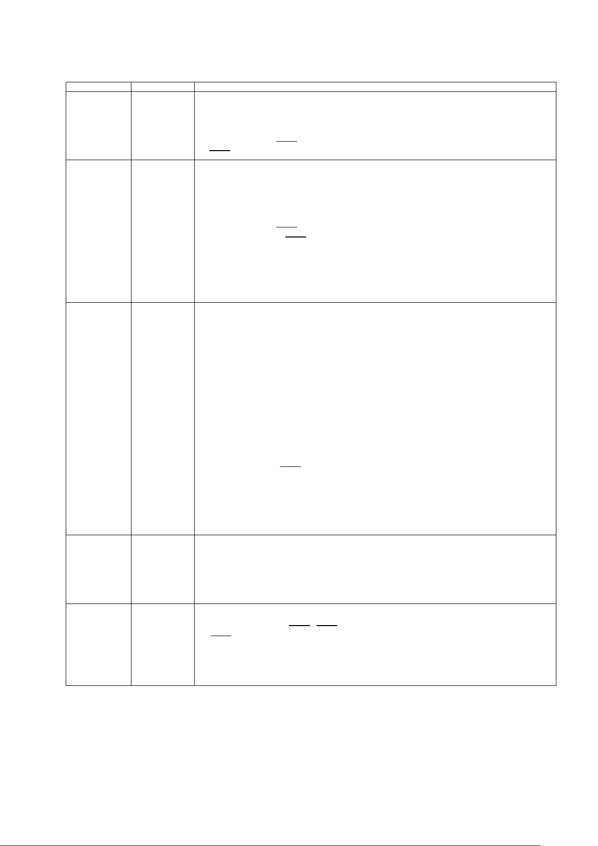
Document change history
First Edition
Sep. 11, 2009
Initial edition
Second Edition
Nov. 13, 2009
Added the descriptions on CPU core "ARM" and "PALMiCE3 ARM (JTAG200)" to Technical
”SRST signal is an open-collector output."
Third Edition
Mar. 04, 2011
PALMiCE3 CM3(ETM200) has already been released (Dec. 2009).
When you use them, please contact us.
Fourth Edition
Sep. 18, 2015
Added an item to Applicable products:
products and the product purchase chart.
Fifth Edition
Mar. 04, 2016
In accordance with PALMi C E 3 CM3(ETM200) sales termination, deleted PA L M i CE3
Added a note that SWO signal is unused in ①, ③ and ⑦.
Sixth Edition
Oct. 30,2018
Updated Table of contents
by one.
・
Information reference chart and Product purchase chart.
・ Corrected the Product purchase chart.
Technical Information ④ and ⑥ correspond to PALMiCE3 CM3 (ETM200) only.
However, PALMiCE3 CM3(ETM200) is a product to be released in the future.
・ Added the note on
・
Deleted the following description:
”To be released in the future.”
・ “Supported connectors”
Added graphic images of the connectors.
・ “Product purchase chart”
Added graphic images of the optional products.
・ Added the note on
・ Changed the note on
・ Deleted CPU core options from Technical Information reference chart and Product purchase
chart.
For supported CPUs, refer to Product Summary of respective products up on our website.
・ Deleted the description of the case where ETM is not used and half-pitch (1.27mm) connector is
used.
SRST signal in respective signal tables.
SRST signal in respective signal tables.
TRST signal in respective signal tables.
・
PALMiCE2H ARM (ETM383)
・ Following addition of an item to Applicable products mentioned above, added the description on
PALMiCE2H to Technical Information reference chart and Product purchase chart.
・ Following addition of an item to Applicable products mentioned above, added ⑦⑧⑨⑩ to pages
on target interface details.
・ Placed specifications of the target interface on the debugger side.
PALMiCE3 PALMiCE3 JTAG200 model Hardware Manual)
PALMiCE2H Extracted from PALMiCE2H ARM User's Manual)
・ Supported connectors – 38-pin Mictor connector
Changed the recommended connectors.
[Before change] 2-767004-2 / 767054-1 / 767061 (* RoHS-non-compliant products)
[After change] 2-5767004-2 / 5767054-1 / 5767061-1 (*RoHS-compliant products)
・ Supported connectors
Added the note.
・ Product purchase chart
Added ”PALMiCE3-ARM (JTAG200)” to ⑦ to ⑩.
・ Added notes on the
JTAG interface).
・ Added ⑥ (Using 20-pin 1.27 mm-pitch connector + JTAG interface).
・ According to the above addition, incremented the heading number ⑥ and subsequent numbers
by one.
・ In accordance with J-STICK sales termination, deleted J-STICK descriptions from the applicable
・
CM3(ETM200) descriptions from the applicable products and the product purchase chart.
・ Product purchase chart
Added “PALMiCE3 CM3(JTAG200)” to ①, ②, ③, ⑥, ⑦, ⑧, ⑨, ⑩ and ⑪.
・ Added an item to Applicable products:
PALMiCE3 CM3(JTAG200)
・
・
・ About ②, ⑥, ⑪
・Annotation added for
TRST signal related changes in the Target connection reference diagram
・
・ Reference note added for RZ/A and RZ/T series /SRST, /TRST signals
・ Added ⑧ (Using 10-pin 1.27 mm-pitch connector + JTAG interface).
・ According to the above addition, incremented the heading number ⑧ and subsequent numbers
TRST signal described in ② (Using 20-pin 2.54 mm-pitch connector +
TRST, SRST signals
1
Page 4
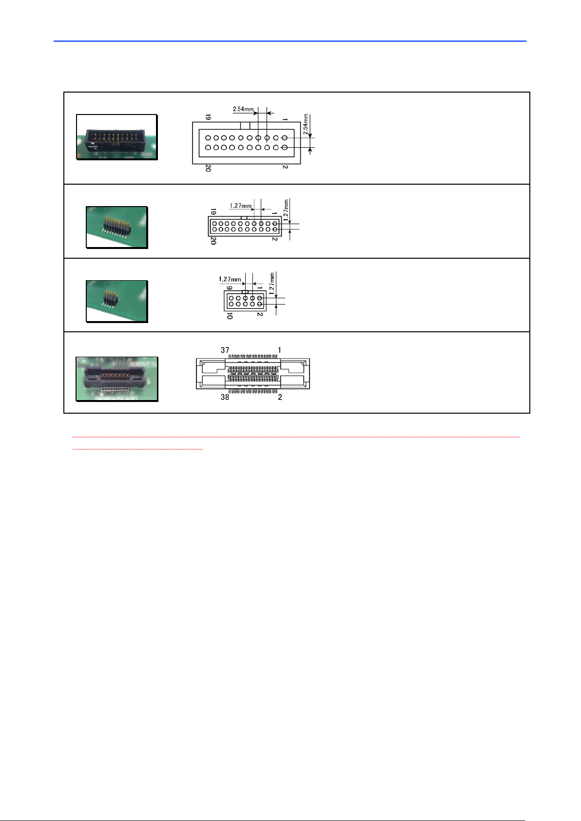
Technical Information on JTAG / SWD / SWV / ETM ARM-related Target Interface Oct. 30, 2018 (Sixth Edition)
20-pin 2.54mm-pitch connector
(Top view on the target board)
Model : XG4C-2031
20-pin 1.27mm-pitch connector
(Top view on the target board)
Model : FTSH-110 -01-L-DV-K
10-pin 1.27mm-pitch connector
(Top view on the target board)
Model : FTSH-105-01-L-DV-K
38-pin Mictor connector
(Top view on the target board)
2-5767004-2 / 5767054-1 / 5767061-1
* Please look at the pin configuration diagram and make sure that the connector is in the right
direction before connecting.
Supported connectors
(For detailed dimensions of the connectors, refer to the documentations by respective manufacturers of the connectors.)
Recommended connector
Manufacturer: OMRON Corporation
Recommended connector
Manufacturer: Samtec, Inc.
Recommended connector
Manufacturer: Samtec, Inc.
Recommended connector
Manufacturer: AMP
Model : Mictor connector
Moreover, please check the pin number in the corresponding signal table and make sure the signal and the pin
numbers match.
Applicable products
This manual is applicable for the following products.
PALMiCE3 ARM (JTAG200)
PALMiCE3 CM3 (JTAG200)
PALMiCE2H ARM (ETM383)
2
Page 5
Technical Information on JTAG / SWD / SWV / ETM ARM-related Target Interface Oct. 30, 2018 (Sixth Edition)
interface
SWV
implemented on the target system
Information No.
⑤
38-pin Mictor connector
To Technical Information reference chart 2
②
⑥
⑧
④
①
③
⑦
Choose a connector to
target system
JTA G
USE ETM
38-pin Mictor connector
No.
⑨
Demultiplex mode
⑩
⑪
⑫
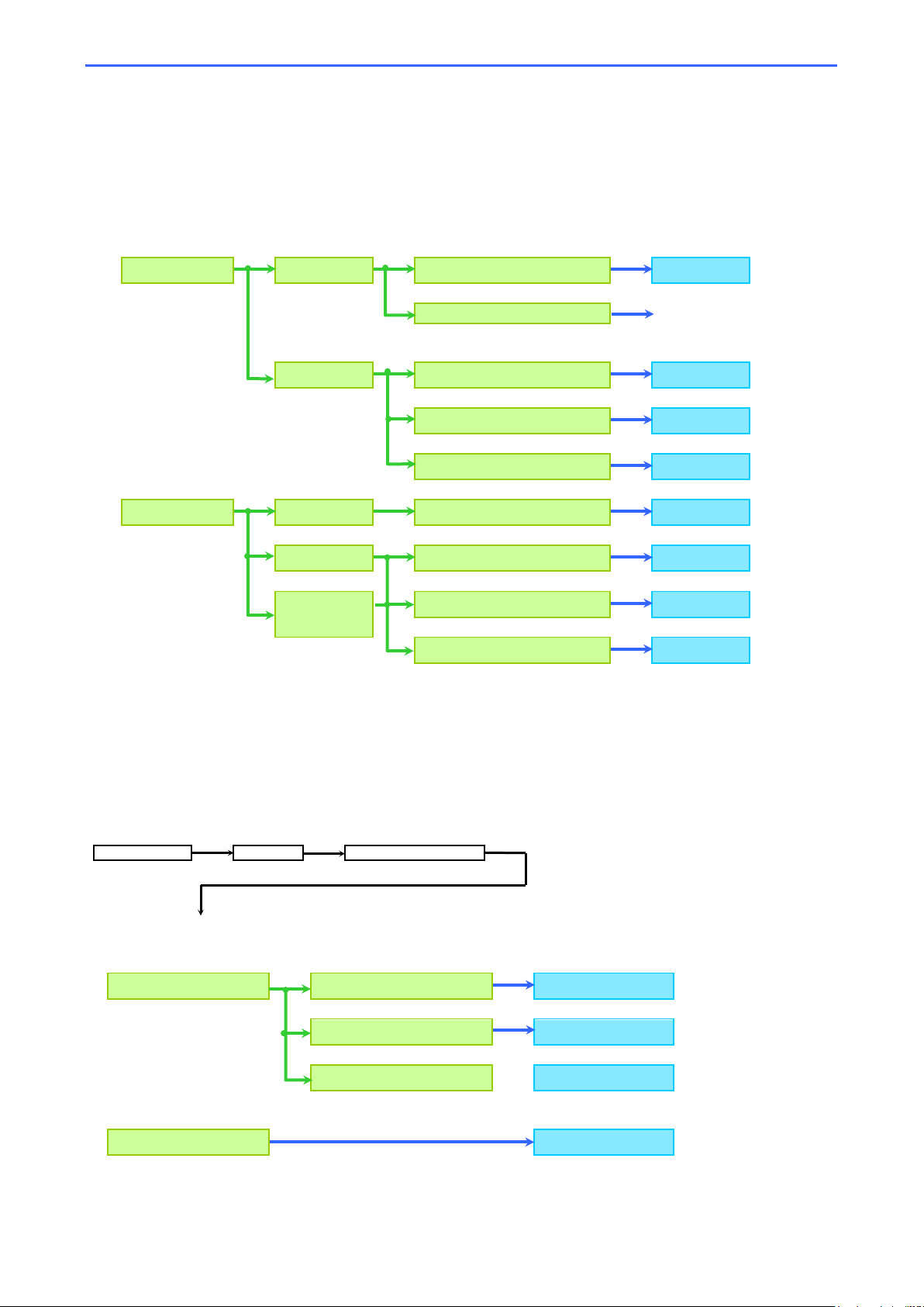
Technical Information reference chart 1
Depending on the target interface you use, Technical Information you should refer to will be different.
Based on the chart below, consult the applicable Technical Information.
Debugging
ETM
Choose a connector to be
Technical
JTA G USE ETM 20-pin 1.27mm-pitch connector
NOT USE ETM 20-pin 2.54mm-pitch connector
SWD USE ETM
USE SWV 20-pin 2.54mm-pitch connector
Neither use
ETM nor SWV
* : Only those combinations available for selection are given. For other combinations, please contact us.
Technical Information reference chart 2
Debugging
interface
ETM
SWV
be implemented on the
20-pin 1.27mm-pitch connector
10-pin 1.27mm-pitch connector
20-pin 1.27mm-pitch connector
20-pin 1.27mm-pitch connector
10-pin 1.27mm-pitch connector
CPU core Mode
ARM7, ARM9
AR M 11, Cortex
Technical Information
Normal mode
Multiplex mode
* : Only those combinations available for selection are given.
3
Page 6
Technical Information on JTAG / SWD / SWV / ETM ARM-related Target Interface Oct. 30, 2018 (Sixth Edition)
Technical
Information No.
Required optional
product
①
PALMiCE3 ARM (JTAG200)
PALMiCE3 ARM64 (JTAG200)
PALMiCE3 CM3 (JTAG200)
②
PALMiCE3 ARM (JTAG200)
PALMiCE3 ARM64 (JTAG200)
PALMiCE3 CM3 (JTAG200)
PALMiCE2H ARM (ETM383)
+
ADP-ETM-JTAG2 0
③
PALMiCE3 ARM (JTAG200)
+
SWJ-PRB-MIL 20-20HP
PALMiCE3 ARM64 (JTAG200)
+
SWJ-PRB-MIL 20-20HP
PAL Mi CE3 CM3 (JTAG200)
+
SWJ-PRB-MIL 20-20HP
PALMiCE2H ARM (ETM383)
④
PALMiCE2H ARM (ETM383)
⑤
⑥
PAL Mi CE3 ARM (JTAG200)
+
SWJ-PRB-MIL 20-20HP
PALMiCE3 ARM64 (JTAG200)
+
SWJ-PRB-MIL 20-20HP
PALMiCE3 CM3 (JTAG200)
+
SWJ-PRB-MIL 20-20HP
⑦
PALMiCE3 ARM (JTAG200)
+
SWJ-PRB-MIL 20-10HP
⑧
PALMiCE3 ARM64 (JTAG200)
+
SWJ-PRB-MIL 20-10HP
PALMiCE3 CM3 (JTAG200)
+
SWJ-PRB-MIL 20-10HP
⑨
PALMiCE2H ARM (ETM383)
⑩
PALMiCE3 ARM (JTAG200)
+
ADP-JTA G2 0-ETM
⑪
PALMiCE3 CM3 (JTAG200)
+
ADP-JTA G2 0-ETM
⑫
PALMiCE2H ARM (ETM383)
PALMiCE3 ARM (JTAG200)
+
ADP-JTAG 20 -ETM
PALMiCE3 ARM64 (JTAG200)
+
ADP-JTA G2 0-ETM
PALMiCE3 CM3 (JTAG200)
+
ADP-JTA G2 0-ETM
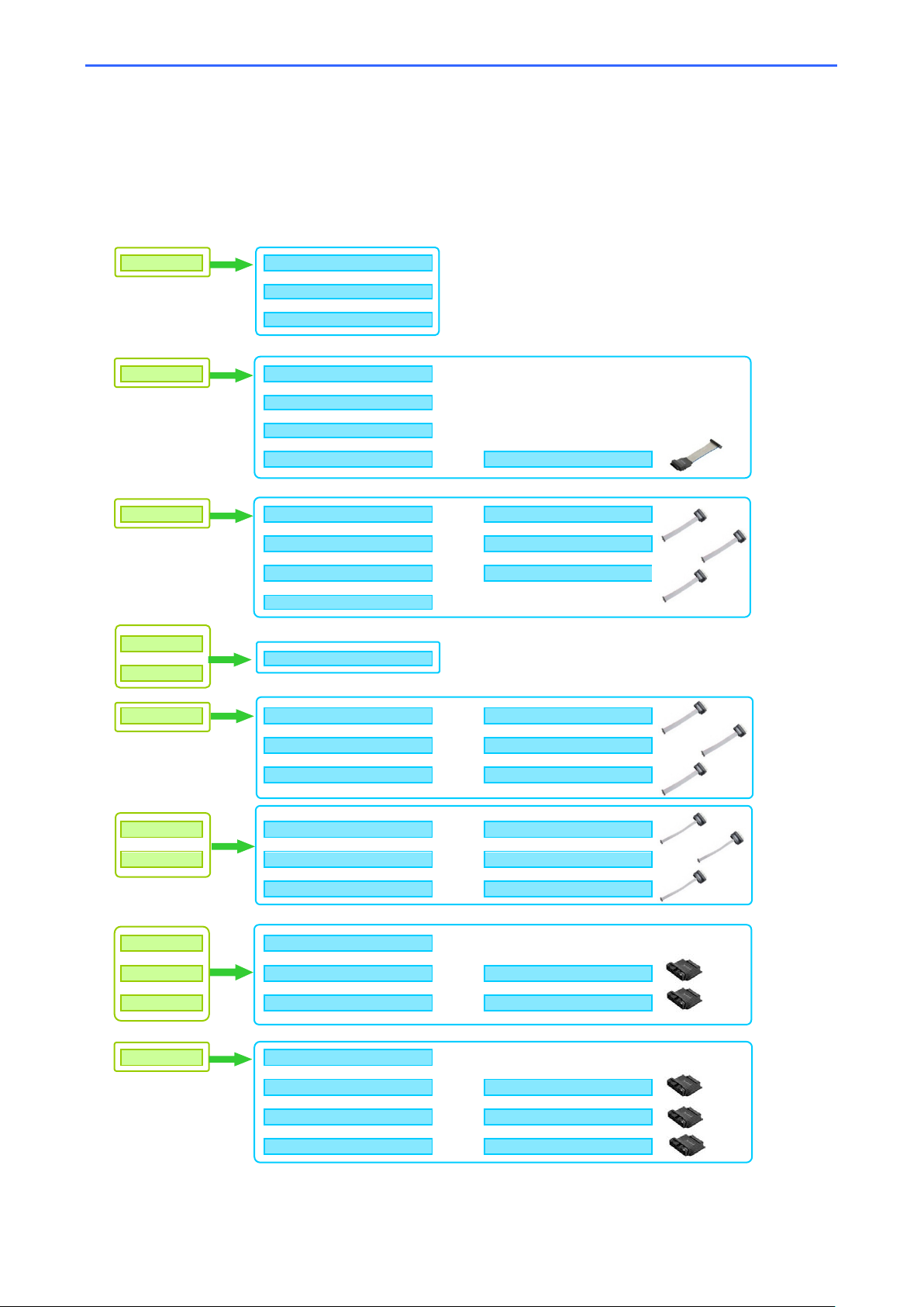
Product purchase chart
Depending on the target interface you use, the composition of product and optional product you should purchase will differ.
Based on the Technical Information No. (See "Technical Information reference chart" on the previous page), choose the product.
: Only those products available for selection are given.
*
Product name *1
*1 : For the CPUs supported by respective products, refer to Product Summary of respective products up on Computex website.
4
Page 7
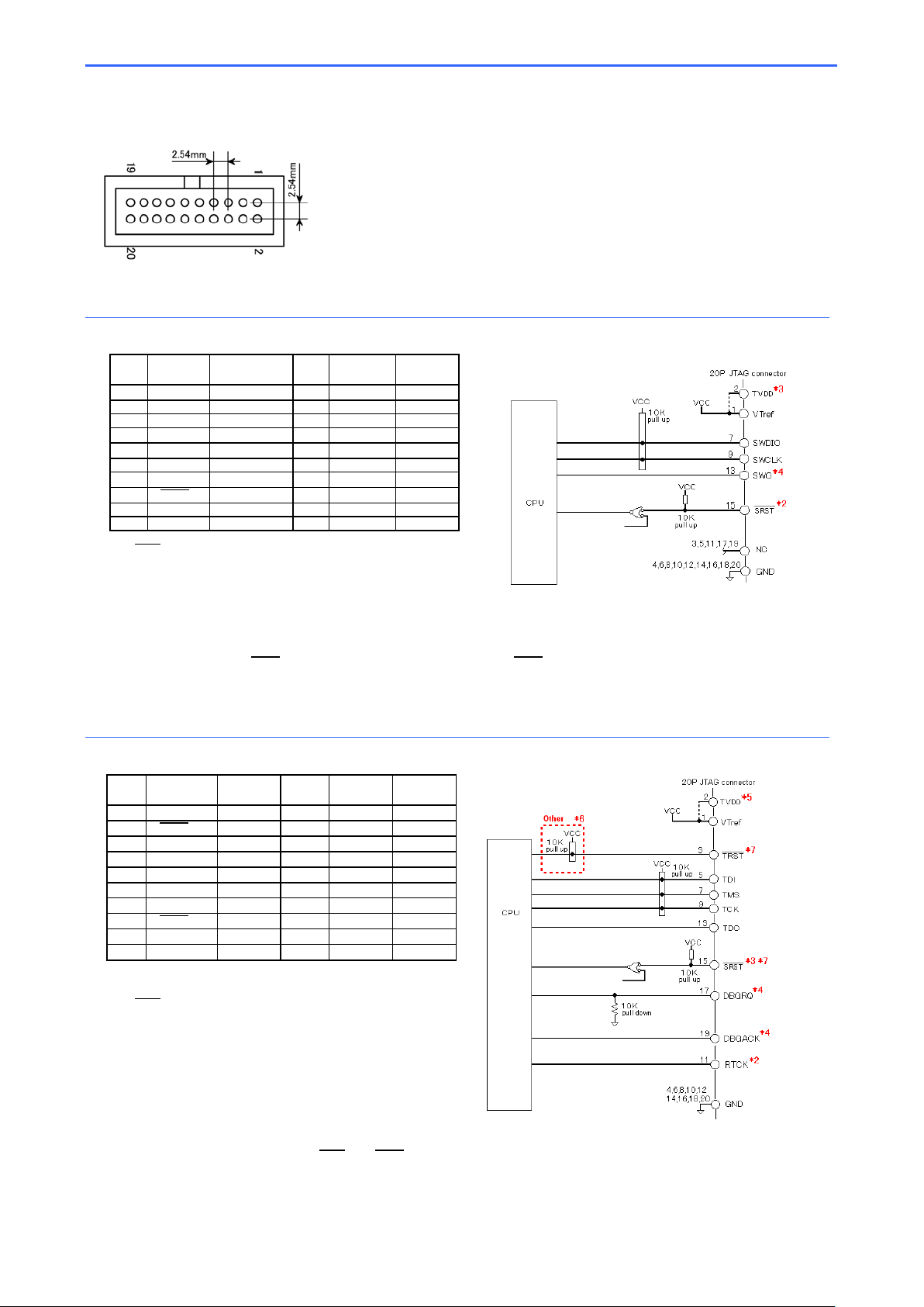
Technical Information on JTAG / SWD / SWV / ETM ARM-related Target Interface Oct. 30, 2018 (Sixth Edition)
■
Target connector specifications
(Top view on the target board)
Recommended connector
Model: XG4C-2031
numbers match.
①
Signals
Pin
No.
Input/
Output
Pin
No.
Input/
Output
1
VTref
Output
2
TVDD*3
Output
3
NC 4
GND
5 NC 6
GND
7
SWDIO
Input/Output
8
GND
9 SWCLK
Input
10
GND
11
NC 12
GND
13
SWO*4
Output
14
GND
15
SRST*2
16
GND
17
NC 18
GND
19
NC 20
GND
signal.
Target connection reference diagram
②
Signals
Target connection reference diagram
Pin
No.
Input/
Output
Pin
No.
Input/
Output
1
VTref
Output
2
TVDD*5
Output
3
TRST
*6 *7
Input
4
GND
5 TDI
Input
6
GND
7 TMS
Input
8
GND
9 TCK
Input
10
GND
11
RTCK*2
Output
12
GND
13
TDO
Output
14
GND
15
SRST
*3 *7
Input
16
GND
17
DBGRQ*4
Input
18
GND
19
DBGACK*4
Output
20
GND
20-pin 2.54mm-pitch connector
Manufacturer: OMRON Corporation
(For detailed dimensions of the connector, refer to the documentation by manufacturer of the connector.)
*Please look at the pin configuration diagram above and make sure that the connector is in
the right direction before connecting.
Please check the pin number in the signal table above and make sure the signal and the pin
SWD interface
Signal
*1: Input/output is based on the target system.
*2:
SRST signal is an open-collector output.
Establish wired-OR connection to "power-on-reset" or "system
reset" on the target system, or if wired-OR circuit is not available,
connect with OR circuit.
*3: The signal is not used by Computex-made debugger; it can be left
unconnected.
*4: If the SWV(Serial Wire Viewer) is not used for debugging or the CPU
does not support the SWV, do not connect anything to the SWO
This interface does not use TRST. If the target CPU presents a pin specifically for TRST, pull it up with 10K ohmic value.
Keep the length of wirings from CPU to the target connector as short as possible. If the length gets long, it could possibly be a factor contributing to
malfunction.
JTAG interface
Signal
*1
*1
Signal
Signal
*1
*1
*1: Input/output is based on the target system.
*2: If the CPU does not present the pin or if you do not use RTCK,
leave it as N.C..
*3:
SRST signal is an open-collector output.
Establish wired-OR connection to "power-on-reset" or "system
reset" on the target system, or if wired-OR circuit is not available,
connect with OR circuit.
*4: In the CPUs that do not present this signal, leave the pin
unconnected in open state.
*5: The signal is not used by Computex-made debugger; it can be left
unconnected.
*6: In come CPUs, a pulldown many be necessary. Refer the CPU
datasheet and make the necessary pull up/pull down changes if
required.
*7: Refer to the reference diagram [Reference:RZ/A and RZ/T series
/SRST, /TRST reference diagram] for
Renesas electronics RZ/A and RZ/T series.
Keep the length of wirings from CPU to the target connector as short as possible. If the length gets long, it could possibly be a factor contributing to
malfunction.
SRST and TRST signals for
5
Page 8
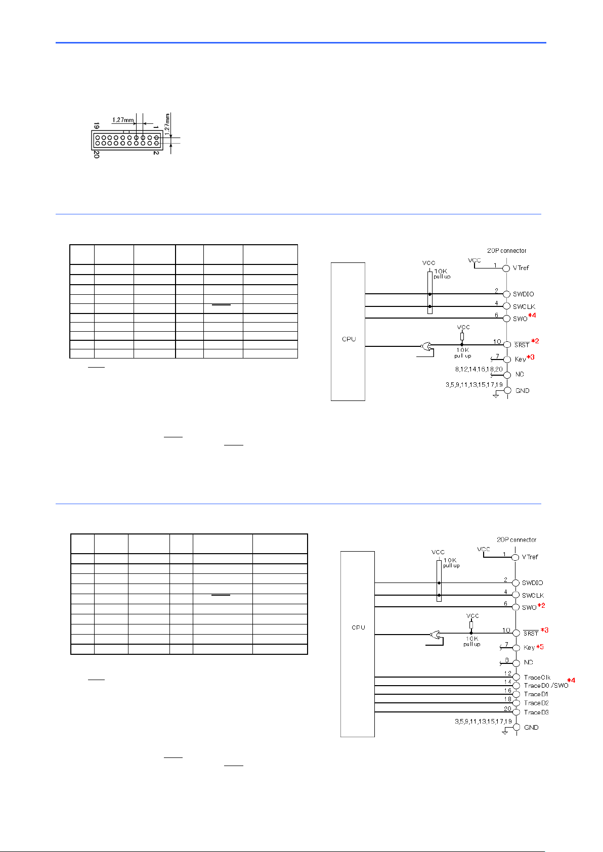
Technical Information on JTAG / SWD / SWV / ETM ARM-related Target Interface Oct. 30, 2018 (Sixth Edition)
■
Target connector specifications
Recommended connector
Model: FTSH-110 -01-L-DV-K
(For detailed dimensions of the connector, refer to the documentation by manufacturer of the connector.)
numbers match.
③
Signals
Pin
No.
Input/
Output
Pin
No.
Input/
Output
1
Vtref
Output
2
SWDIO
Input/Output
3
GND 4
SWCLK
Input
5
GND 6
SWO
*4z
Output
7
Key*3
8 NC
9
GND 10
SRST*2
Input
11
GND 12
NC 13
GND 14
NC 15
GND 16
NC 17
GND 18
NC 19
GND 20
NC
Target connection reference diagram
④
Signals
Pin
No.
Input/
Output*1
Pin
No.
Input/
Output*1
1
Vtref
Output
2
SWDIO
Input/Output
3
GND 4
SWCLK
Input
5
GND 6
SWO*2
Output
7
Key*5
8 NC
Input
9
GND 10
SRST*3
Input
11
GND 12
TraceClk
Output
13
GND 14
TraceD0/SWO*4
Output
15
GND 16
TraceD1
Output
17
GND 18
TraceD2
Output
19
GND 20
TraceD3
Output
Target connection reference diagram
20-pin 1.27mm-pitch connector
Manufacturer: Samtec, Inc.
*Please look at the pin configuration diagram above and make sure that the connector is in
the right direction before connecting.
Please check the pin number in the signal table above and make sure the signal and the pin
(Top view on the target board)
SWD interface
Signal
*1: Input/output is based on the target system.
*2:
SRST signal is an open-collector output.
Establish wired-OR connection to "power-on-reset" or "system
reset" on the target system, or if wi red-OR circuit is not available,
connect with OR circuit.
*3: "Key" is intended for protection against wrong insertion.
*4: If the SWV(Serial Wire Viewer) is not used for debugging or the
CPU does not support the SWV, do not connect anything to the
SWO signal.
This interface does not use TRST.
If the target CPU presents a pin specifically for
Keep the length of wirings from CPU to the target connector as short as possible. If the length gets long, it could possibly be a factor contributing to
malfunction.
*1
Signal
TRST, pull it up with 10K ohmic value.
*1
SWD interface + Trace
Signal
Signal
*1: Input/output is based on the target system.
*2: Connect the signal dedicated to SWO. The pin can be left N.C. if you
are using Pin No. 14 as SWO (See *4).
*3:
SRST signal is an open-collector output.
Establish wired-OR connection to "power-on-reset" or "system reset"
on the target system, or if wired-OR circuit is not available, connect
with OR circuit.
*4: In some CPUs, SW O and TraceD0 are multiplexed.
In the case of such pin, connect SWO signal not to Pin No. 6 but to Pin
No.14 even when you intend to use Pin No. 14 as SW O, not as
TraceD0.
*5: "Key" is intended for protection against wrong insertion.
This interface does not use TRST.
If the target CPU presents a pin specifically for
Keep the length of wirings from CPU to the target connector as short as possible. If the length gets long, it could possibly be a factor contributing to
malfunction.
TRST, pull it up with 10K ohmic value.
6
Page 9
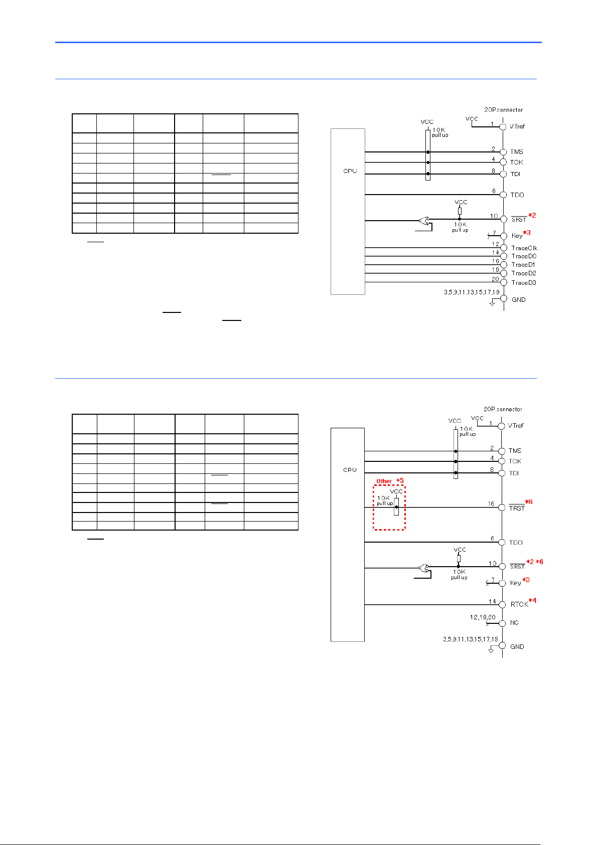
Technical Information on JTAG / SWD / SWV / ETM ARM-related Target Interface Oct. 30, 2018 (Sixth Edition)
⑤
Signals
Pin
No.
Input/
Output*1
Pin
No.
Input/
Output*1
1
Vtref
Output
2
TMS
Input/Output
3
GND 4
TCK
Input
5
GND 6
TDO
Output
7
Key*3
8 TDI
Input
9
GND 10
SRST*2
Input
11
GND 12
TraceClk
Output
13
GND 14
TraceD0
Output
15
GND 16
TraceD1
Output
17
GND 18
TraceD2
Output
19
GND 20
TraceD3
Output
Target connection reference diagram
⑥
Signals
Pin
No.
Input/
Output*1
Pin
No.
Input/
Output*1
1
Vtref
Output
2
TMS
Input/Output
3
GND 4
TCK
Input
5
GND 6
TDO
Output
7
Key*3
8 TDI
Input
9
GND 10
SRST
Input
11
GND 12
NC
13
GND 14
RTCK*4
Output
15
GND 16
TRST
*5 *6
Input
17
GND 18
NC
19
GND 20
NC
Target connection reference diagram
JTAG interface + Trace
Signal
*1: Input/output is based on the target system.
*2:
SRST signal is an open-collector output.
Establish wired-OR connection to "power-on-reset" or "system reset"
on the target system, or if wired-OR circuit is not available, connect
with OR circuit.
*3: "Key" is intended for protection against wrong insertion.
Signal
This interface does not use TRST.
If the target CPU presents a pin specifically for
Keep the length of wirings from CPU to the target connector as short as possible. If the length gets long, it could possibly be a factor contributing to
malfunction.
TRST, pull it up with 10K ohmic value.
JTAG interface
Signal
*1: Input/output is based on the target system.
*2:
SRST signal is an open-collector output.
Establish wired-OR connection to "power-on-reset" or "system reset"
on the target system, or if wired-OR circuit is not available, connect
with OR circuit.
*3: "Key" is intended for protection against wrong insertion.
*4: If the CPU does not present the pin or if you do not use RTCK, leave
it as N.C..
*5: In come CPUs, a pulldown many be necessary. Refer the CPU
datasheet and make the necessary pull up/pull down changes if
required.
*6: Refer to the reference diagram [Reference:RZ/A and RZ/T series
/SRST, /TRST reference diagram] for SRST and TRST signals for
Renesas electronics RZ/A and RZ/T series.
Signal
*2 *6
Keep the length of wirings from CPU to the target connector as short as possible. If the length gets long, it could possibly be a factor contributing to
malfunction.
7
Page 10
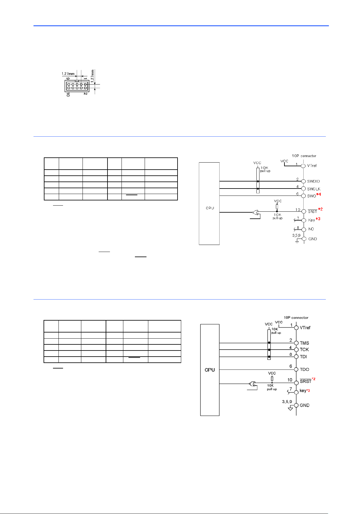
Technical Information on JTAG / SWD / SWV / ETM ARM-related Target Interface Oct. 30, 2018 (Sixth Edition)
■
Target connector specifications
Model: FTSH-105-01-L-DV-K
(For detailed dimensions of the connector, refer to the documentation by manufacturer of the connector.)
numbers match.
⑦
Signals
Pin
No.
Input/
Output
Pin
No.
Input/
Output
1
VTref
Output
2
SWDIO
Input/Output
3
GND
4 SWCLK
Input
5
GND
6
SWO*4
Output
7
Key*3
8 NC
Input
9
GND
10
SRST*2
Input
Target connection reference diagram
⑧
Signals
Pin
No.
Input/
Output*1
Pin
No.
Input/
Output*1
1
Vtref
Output
2
TMS
Input/Output
3
GND 4
TCK
Input
5
GND 6
TDO
Output
7
Key*3
8 TDI
Input
9
GND 10
SRST*2
Input
Target connection reference diagram
10-pin 1.27mm-pitch connector
Recommended connector
Manufacturer: Samtec, Inc.
(Top view on the target board)
*Please look at the pin configuration diagram above and make sure that the connector is in
the right direction before connecting.
Please check the pin number in the signal table above and make sure the signal and the pin
SWD interface
Signal
*1: Input/output is based on the target system.
*2:
SRST signal is an open-collector output.
Establish wired-OR connection to "power-on-reset" or "system
reset" on the target system, or if wired-OR circuit is not available,
connect with OR circuit.
*3: "Key" is intended for protection against wrong insertion.
*4: If the SWV(Serial Wire Viewer) is not used for debugging or the
CPU does not support the SWV, do not connect anything to the
SWO signal.
This interface does not use TRST.
If the target CPU presents a pin specifically for
Keep the length of wirings from CPU to the target connector as short as possible. If the length gets long, it could possibly be a factor contributing to
malfunction.
*1
Signal
TRST, pull it up with 10K ohmic value.
*1
JTAG interface
Signal
*1: Input/output is based on the target system.
*2:
SRST signal is an open-collector output.
Establish wired-OR connection to "power-on-reset" or "system reset"
on the target system, or if wired-OR circuit is not available, connect
with OR circuit.
*3: "Key" is intended for protection against wrong insertion.
Keep the length of wirings from CPU to the target connector as short as possible. If the length gets long, it could possibly be a factor contributing to
malfunction.
Signal
8
Page 11
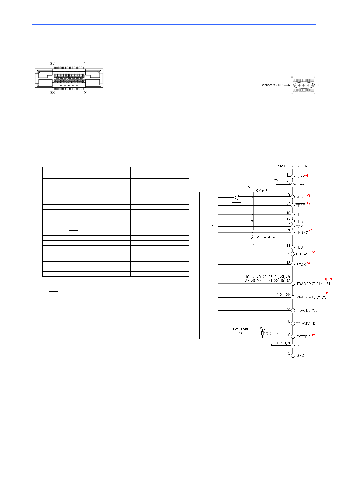
Technical Information on JTAG / SWD / SWV / ETM ARM-related Target Interface Oct. 30, 2018 (Sixth Edition)
■
Target connector specifications
(Top view on the target board)
2-767004-2 / 767054-1 / 767061
In mounting ETM connector, place it to the position as close as
ETM connector.
In addition, you will need to
connect the Grand Bus
(For detailed dimensions of the connector, refer to the documentation by manufacturer of the connector.)
match.
⑨
Signals
Pin
No.
Input/
Output*1
Pin
No.
Input/
Output*1
1
NC
2 NC
3 NC
4 NC
5 GND
6 TRACECLK
Output
7
DBGRQ*2
Input
8
DBGACK*2
Output
9
SRST*3
Input
10
EXTTRIG*5
Input
11
TDO
Output
12
VTref
Output
13
RTCK*4
Output
14
TVDD*6
Output
15
TCK
Input
16
TRACEPKT7
*8*9
Output
17
TMS
Input
18
TRACEPKT6
*8*9
Output
19
TDI
Input
20
TRACEPKT5
*8*9
Output
21
TRST*7
Input
22
TRACEPKT4
*8*9
Output
23
TRACEPKT15
*8*9
Output
24
TRACEPKT3
*8*9
Output
25
TRACEPKT14
*8*9
Output
26
TRACEPKT2
*8*9
Output
27
TRACEPKT13
*8*9
Output
28
TRACEPKT1
*8*9
Output
29
TRACEPKT12
*8*9
Output
30
TRACEPKT0
*8*9
Output
31
TRACEPKT11
*8*9
Output
32
TRACESYNC
Output
33
TRACEPKT10
*8*9
Output
34
PIPES TAT2*9
Output
35
TRACEPKT9
*8*9
Output
36
PIPES TAT1*9
Output
37
TRACEPKT8
*8*9
Output
38
PIPES TAT0*9
Output
Target connection reference diagram
38-pin Mictor connector
possible to CPU so that wiring pattern length will be minimized.
Recommended connector
Also in mounting JTAG connector, place it to the position close to
Manufacturer :AMP
Model : Mictor connector
Leads of ETM connector to
the GND.
*Please look at the pin configuration diagram above and make sure that the connector is in the right direction
before connecting.
Please check the pin number in the signal table above and make sure the signal and the pin numbers
JTAG interface + ETM - Normal mode
Signal
Signal
*1: Input/output is based on the target system.
*2: In the CPUs that do not present this signal, leave the pin unconnected in open
state.
*3:
SRST signal is an open-collector output.
Establish wired-OR connection to "power-on-reset" or "system reset" on the
target system, or if wired-OR circuit is not available, connect with OR circuit.
*4: If the CPU does not present the pin or if you do not use RTCK, leave it as
N.C..
*5: The signal is not used by Computex-made debugger.
*6: The signal is not used by Computex-made debugger; it can be left
unconnected.
*7: If the target CPU presents a pin specifically for
ohmic value.
*8: If the trace data is of 4-bit, connect signals TRACEPKT4 - 15, or if of 8-bit, connect
signals TRACEPKT8 - 15, to GND.
*9: For the names of signals corresponding to respective pin No., see the table of
Signals.
Keep the length of wirings from CPU to the target connector as short as possible. If the length gets long, it could possibly be a factor contributing to
malfunction.
TRST, pull it up with 10K
9
Page 12
Technical Information on JTAG / SWD / SWV / ETM ARM-related Target Interface Oct. 30, 2018 (Sixth Edition)
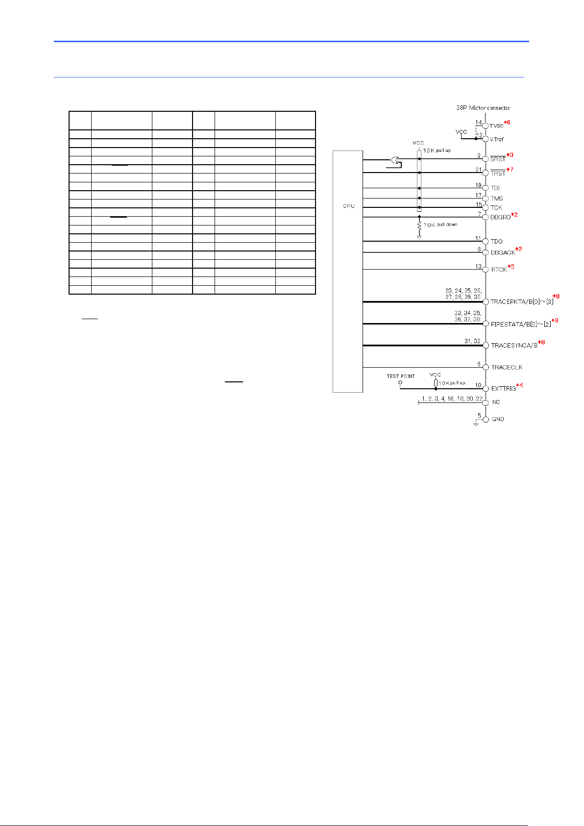
⑩
Signals
Pin
No.
Input/
Output
Pin
No.
Input/
Output
1
NC
2 NC
3
NC
4 NC
5
GND
6 TRACECLK
Output
7
DBGRQ *2
Input
8
DBGACK *2
Output
9
SRST*3
Input
10
EXTTRIG *4
Input
11
TDO
Output
12
VTref
Output
13
RTCK *5
Output
14
TVDD *6
Output
15
TCK
Input
16
NC
17
TMS
Input
18
NC
19
TDI
Input
20
NC
21
TRST *7
Input
22
NC
23
TRACEPKTB3*8
Output
24
TRACEPKTA3*8
Output
25
TRACEPKTB2*8
Output
26
TRACEPKTA2*8
Output
27
TRACEPKTB1*8
Output
28
TRACEPKTA1*8
Output
29
TRACEPKTB0*8
Output
30
TRACEPKTA0*8
Output
31
TRACESYNCB*8
Output
32
TRACESYNCA*8
Output
33
PIPESTATB2*8
Output
34
PIPESTATA2*8
Output
35
PIPESTATB1*8
Output
36
PIPESTATA1*8
Output
37
PIPESTATB0*8
Output
38
PIPESTATA0*8
Output
Target connection reference diagram
JTAG interface + ETM – Demultiplex mode
Signal
*1: Input/output is based on the target system.
*2: In the CPUs that do not present this signal, leave the pin unconnected in open
state.
*3:
SRST signal is an open-collector output.
Establish wired-OR connection to "power-on-reset" or "system reset" on the
target system, or if wired-OR circuit is not available, connect with OR circuit.
*4: The signal is not used by Computex-made debugger.
*5: f the CPU does not present the pin or if you do not use RTCK, leave it as
N.C..
*6: The signal is not used by Computex-made debugger; it can be left
unconnected.
*7: If the target CPU presents a pin specifically for
ohmic value.
*8: For the names of signals corresponding to respective pin No., see the table of
Signals.
*1
Signal
TRST, pull it up with 10K
*1
Keep the length of wirings from CPU to the target connector as short as possible. If the length gets long, it could possibly be a factor contributing to
malfunction.
10
Page 13
Technical Information on JTAG / SWD / SWV / ETM ARM-related Target Interface Oct. 30, 2018 (Sixth Edition)
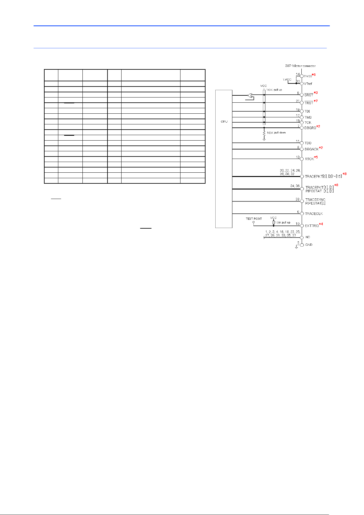
⑪
Signals
Pin
No.
Input/
Output
Pin
No.
Input/
Output
1
NC 2
NC
3
NC 4
NC
5
GND
6 TRACECLK
Output
7
DBGRQ*2
Input
8
DBGACK*2
Output
9
SRST*3
Input
10
EXTTRIG*4
Input
11
TDO
Output
12
VTref
Output
13
RTCK*5
Output
14
TVDD*6
Output
15
TCK
Input
16
NC
17
TMS
Input
18
NC
19
TDI
Input
20
TRACEPKT[14,15]
*8
Output
21
TRST*7
Input
22
TRACEPKT[12,13]
*8
Output
23
NC 24
TRACEPKT[10,11]
*8
Output
25
NC 26
TRACEPKT[8,9]
*8
Output
27
NC 28
TRACEPKT[6,7]
*8
Output
29
NC 30
TRACEPKT[4,5]
*8
Output
31
NC 32
TRACEPKT[0,3]
*8
Output
33
NC 34
PIPESTAT2+TRACEPKT2*8
Output
35
NC 36
PIPESTAT1+TRACEPKT1*8
Output
37
NC 38
PIPESTAT0+TRACESYNC
Output
Target connection reference diagram
JTAG interface + ETM – Multiplex mode
Signal
*1: Input/output is based on the target system.
*2: In the CPUs that do not present this signal, leave the pin unconnected in open
state.
*3:
SRST signal is an open-collector output.
Establish wired-OR connection to "power-on-reset" or "system reset" on the target
system, or if wired-OR circuit is not available, connect with OR circuit.
*4: The signal is not used by Computex-made debugger.
*5: f the CPU does not present the pin or if you do not use RTCK, leave it as N.C..
*6: The signal is not used by Computex-made debugger; it can be left unconnected.
*7: If the target CPU presents a pin specifically for
value.
*8: For the names of signals corresponding to respective pin No., see the table of
Signals.
*1
Signal
TRST, pull it up with 10K ohmic
*1
Keep the length of wirings from CPU to the target connector as short as possible. If the length gets long, it could possibly be a factor contributing to
malfunction.
11
Page 14
Technical Information on JTAG / SWD / SWV / ETM ARM-related Target Interface Oct. 30, 2018 (Sixth Edition)
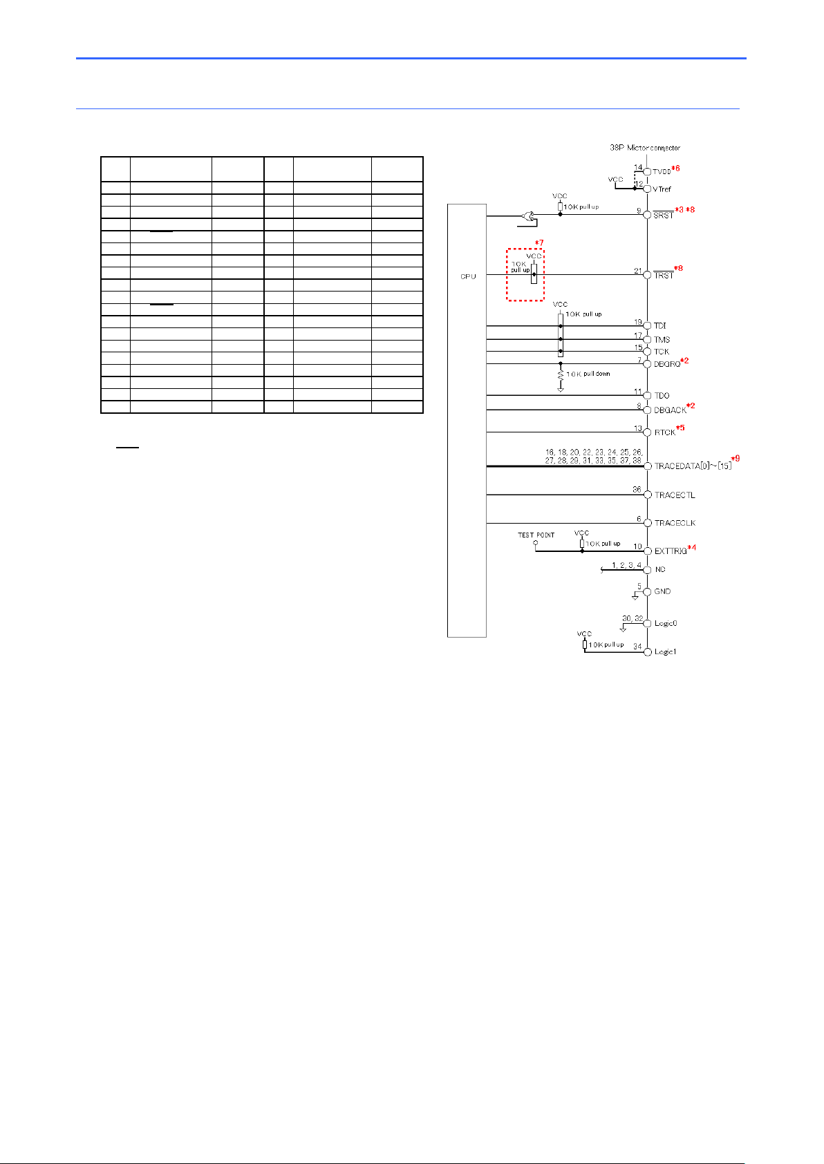
⑫
Signals
Pin
No.
Input/
Output*1
Pin
No.
Input/
Output*1
1
NC
2 NC
3 NC
4 NC
5 GND
6 TRACECLK
Output
7
DBGRQ*2
Input
8
DBGACK*2
Output
9
SRST
*3 *8
Input
10
EXTTRIG*4
Input
11
TDO
Output
12
VTref
Output
13
RTCK*5
Output
14
TVDD*6
Output
15
TCK
Input
16
TRACEDATA[7]
*9
Output
17
TMS
Input
18
TRACEDATA[6]
*9
Output
19
TDI
Input
20
TRACEDATA[5]
*9
Output
21
TRST
*7 *8
Input
22
TRACEDATA[4]
*9
Output
23
TRACEDATA[15]
*9
Output
24
TRACEDATA[3]
*9
Output
25
TRACEDATA[14]
*9
Output
26
TRACEDATA[2]
*9
Output
27
TRACEDATA[13]
*9
Output
28
TRACEDATA[1]
*9
Output
29
TRACEDATA[12]
*9
Output
30
Logic0
Output
31
TRACEDATA[11]
*9
Output
32
Logic0
Output
33
TRACEDATA[10]
*9
Output
34
Logic1
Output
35
TRACEDATA[9]
*9
Output
36
TRACECTL
Output
37
TRACEDATA[8]
*9
Output
38
TRACEDATA[0]
*9
Output
Target connection reference diagram
JTAG interface + ETM / PTM
Signal
*1: Input/output is based on the target system.
*2: In the CPUs that do not present this signal, leave the pin unconnected in
open state.
*3:
SRST signal is an open-collector output.
Establish wired-OR connection to "power-on-reset" or "system reset" on
the target system, or if wired-OR circuit is not available, connect with OR
circuit.
*4: The signal is not used by Computex-made debugger.
*5: If the CPU does not present the pin or if you do not use RTCK, leave it
as N.C..
*6: The signal is not used by Computex-made debugger; it can be left
unconnected.
*7: In come CPUs, a pulldown many be necessary. Refer the CPU datasheet
and make the necessary pull up/pull down changes if required.
*8: Refer to the reference diagram [Reference:RZ/A and RZ/T series /SRST,
/TRST reference diagram] for SRST and TRST signals for Renesas
electronics RZ/A and RZ/T series.
*9: For the names of signals corresponding to respective pin No., see the
table of Signals.
Signal
Keep the length of wirings from CPU to the target connector as short as possible. If the length gets long, it could possibly be a factor contributing to
malfunction.
12
Page 15
Technical Information on JTAG / SWD / SWV / ETM ARM-related Target Interface Oct. 30, 2018 (Sixth Edition)
:
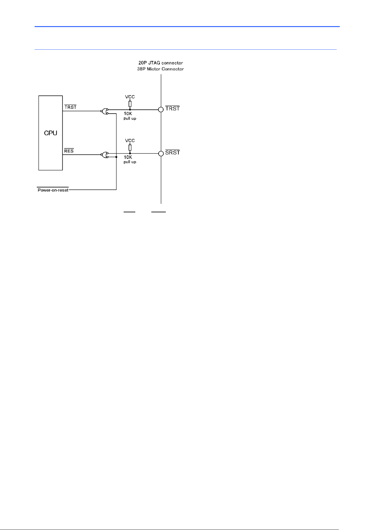
Reference
It may be required to control the RES and TRST CPU pins so that they are in low state at power on. Refer the
CPU datasheet for details.
RZ/A and RZ/T series /SRST, /TRST reference diagram
13
Page 16

Technical Information on JTAG / SWD / SWV / ETM ARM-related Target Interface Oct. 30, 2018 (Sixth Edition)
travellers directl y carry) this product or providing this product for residents outside Japan.
Technical Information on JTAG / SWD / SWV / ETM ARM-related Target Interface (Sixth Edition)
Go through the required procedures as stated under Foreign Exchange and Foreign Trade Control Law in exporting (including the case where
No part of this manual, whether in whole or in part, may be adapted, copied or reproduced without prior permission.
The content of and the specifications of this product are subject to change without prior notice.
Computex Co., Ltd. shall not be held liable for any loss or damage arising from the use of this product although all possible measures have been
taken by Computex Co., Ltd. in good faith to ensure the quality of the product.
Contact us for any questions, feedback, comments, requests or anything of concern to you (or in the event of malfunction) regarding this product or
misprinting or missing information within this manual.
Other names of CPUs etc. mentioned in this manual are trademarks or registered trademarks of their respective manufacturers.
PALMiCE, J-STICK and COMPUTEX are registered trademarks of Computex Co., Ltd. in Japan.
Page 17

PALMiCE3 JTAG200 model
Hardware Manual
(Sixth Edition)
Copyright (C) 2009 Computex Co., Ltd.
Page 18

Precautions For Use
Read the following thoroughly before attempting to use the product.
In the event of exporting the product (including taking it outside of Japan) or supplying the software to
third parties not resident in Japan, make sure that all procedures as stipulated by the Foreign Exchange
and Foreign Trade Act are strictly observed.
The product, the product manual and the software may not be used or reproduced in whole or in part
without prior permission.
Product details and specifications are subject to modification without prior notice for the purpose of
improving reliability, functionality and design.
Note that although a great deal of care has been taken in manufacturing the product, the company does
not guarantee the results of its use.
The product has been manufactured with no intention of it being used for any purpose that requires
extremely high levels of reliability and safety in functions and performance (such as in military
equipment, nuclear power equipment, aerodynamic or space exploration equipment, traffic equipment,
incinerator control equipment, medical equipment, power generation control equipment, equipment
installed on the seabed, safety devices or similar equipment) in which malfunctions or incorrect
operations may result in direct threats or damage to human lives or that may result in serious threats to
society in general. Note that the company refutes all responsibility for damages incurred through these
uses.
Do not install the product in locations subject to excessive amounts of water, humidity, dust, oily vapor,
etc., as it may result in the outbreak of fire, malfunctions or electric shock. Make sure that the correct
power supply and voltage as listed is used.
All copyrights pertaining to CSIDE are the sole property of Computex Co., Ltd..
CSIDE, PALMiCE, and COMPUTEX are registered trademarks of Computex Co., Ltd. in Japan.
All other company names, product names, etc., listed within the product manual are trademarks and
registered trademarks of each individual manufacturer
Page 19

Table of Contents
Chapter 1 Getting Started ............................................................... 1
Chapter 2 PALMiCE3 JTAG200 Hardware
Specifications ............ 4
Chapter 3 Target Interface Specifications ........................... 8
1.1 Introduction .............................................................................................................................................. 1
1.2 Product Composition Contents ................................................................................................ 2
1.3 Connection structure........................................................................................................................ 3
2.1 PALMiCE3 JTAG200 model hardware specifications ........................................... 4
2.2 JTAG200 model specifications ................................................................................................ 4
2.3 Name and function of each part ............................................................................................. 5
2.3.1 Hardware revision ................................................................................................................ 6
How revision sticker reads ......................................................................................................................................................... 6
2.4 External probe ........................................................................................................................................ 7
3.1 Introduction .............................................................................................................................................. 8
3.2 Target interface .................................................................................................................................... 8
3.2.1 Shape of the connector for debugger ................................................................. 8
3.2.2 Dimension of the target cable..................................................................................... 8
3.2.3 Specifications of target interface signals ........................................................... 8
3.2.4 The target interface on PALMiCE3 side ............................................................. 9
Page 20

Chapter 1
Getting Started
1.1
Introduction
PALMiCE3 JTAG200 model is an on-chip debugger that supports ARM-made core CPUs.
Its main features are as follows:
Provides multi-core support
No power supply to PALMiCE3 is required (with VBus support)
Allows downloading to external flash memory and its debugging
Supports on-chip flash memory
Versatile
Supports USB Standard Revision2.0 high-speed and full-speed
Allows downloading of the latest CSIDE from the Internet
Designed with palm-sized, light, and compact body
PALMiCE3 JTAG200 model Hardware Manual Chapter 1 Getting Started 1
Page 21
1.2
Product Composition Contents
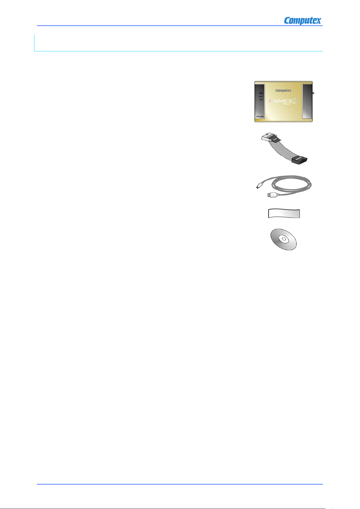
Product composition of PALMiCE3 JTAG200 model is as follows.
・PALMiCE3 JTAG200 model ···································································· x 1
・Target cable (Specifically for PALMiCE3) ···················································· x 1
・USB cable ·························································································· x 1
・Product name sticker ·············································································· x 1
・Software (CD-ROM) *1 ··········································································· x 1
*1 : Its name varies depending on CSIDE, the debugger software you purchased.
PALMiCE3 JTAG200 model Hardware Manual Chapter 1 Getting Started 2
Page 22
1.3
Connection structure
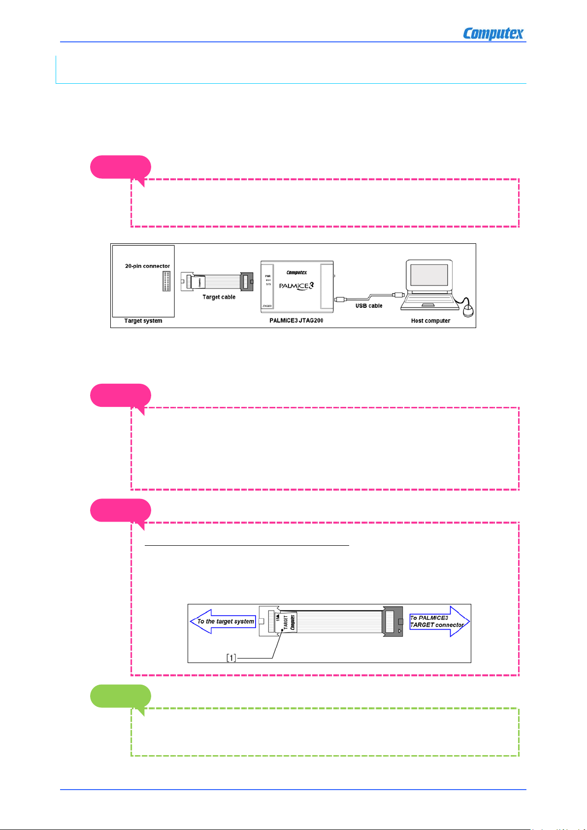
About target cable specifically for PALMiCE3
When establishing connections, connect the connector with a tag ([1] in the
NOTE
NOTE
NOTE
Info.
PALMiCE3 is to be connected to the host computer with the USB cable included with the product. PALMiCE3 is to be connected
to the target system with the target cable included with the product. For details on the target interface, see the next chapter.
To use PALMiCE3, the interface connector for PALMiCE3 use needs to be
mounted on the target system beforehand.
PALMiCE3 JTAG200 model
Connection structure
When connecting the hardware,
if you put too much pressure, stress, or strain on the connector, doing so may cause
damage.
Be careful not to put too much pressure or try not to strain or put stress on the
connector.
・ Make sure to use PALMiCE3-specific target cable made by Computex.
・
illustration) to the target system.
For connection to the target system, optional products such as conversion adapter
are available.
PALMiCE3 JTAG200 model Hardware Manual Chapter 1 Getting Started 3
Page 23
Chapter 2
PALMiCE3 JTAG200 Hardware
Specifications
2.1
PALMiCE3 JTAG200 model hardware specifications
2.2
JTAG200 model specifications
Item
JTAG200 model specifications
Target interface
JTAG, SWD/SWV
Specification of the connector
20-pin MIL connector (Cable length: Approx. 20cm)
the target system side
Target interface voltage
1.0V - 5.5V*1 (Follows target)
LED
PWR ・BSY ・STS
Outside dimensions
95mm(W)X70mm(D)X21mm(H) (Exclusive of connector)
Operating humidity: 35% to 85%RH No condensation
USB host interface
USB(Ver2.0)
AC adapter
Not required (Vbus support)
Current consumption
DC5V ±5% Max. approx. 250mA (from USB VBus)
Weight
78g
*1
2.3.1 Hardware revision
NOTE
PALMiCE3 is a purpose-built debugger for utilizing on-chip debugging feature incorporated in ARM-made cores.
PALMiCE3 incorporates on-chip debugging feature to provide the following functionalities.
This chapter spells out specifications of PALMiCE3 hardware.
Execution and break of the user program
Break by matching any address and data
Force break of the user program
Trace and step executions
Viewing and editing of memory, register, and I/O
Interface on the
main unit side
Operating environment
Specification of the connector on
: Hardware revision "0-0" supports 1.0V - 3.6V.
For hardware revision, see "
OMRON-made XG4C2031 (20-lead)
・
Operating temperature: 5℃ to 40℃
"
PALMiCE3 JTAG200 model Hardware Manual Chapter 2 PALMiCE3 JTAG200 Hardware Specifications 4
Page 24
2.3
Name and function of each part
Connect an optional cable. It is normally not used.
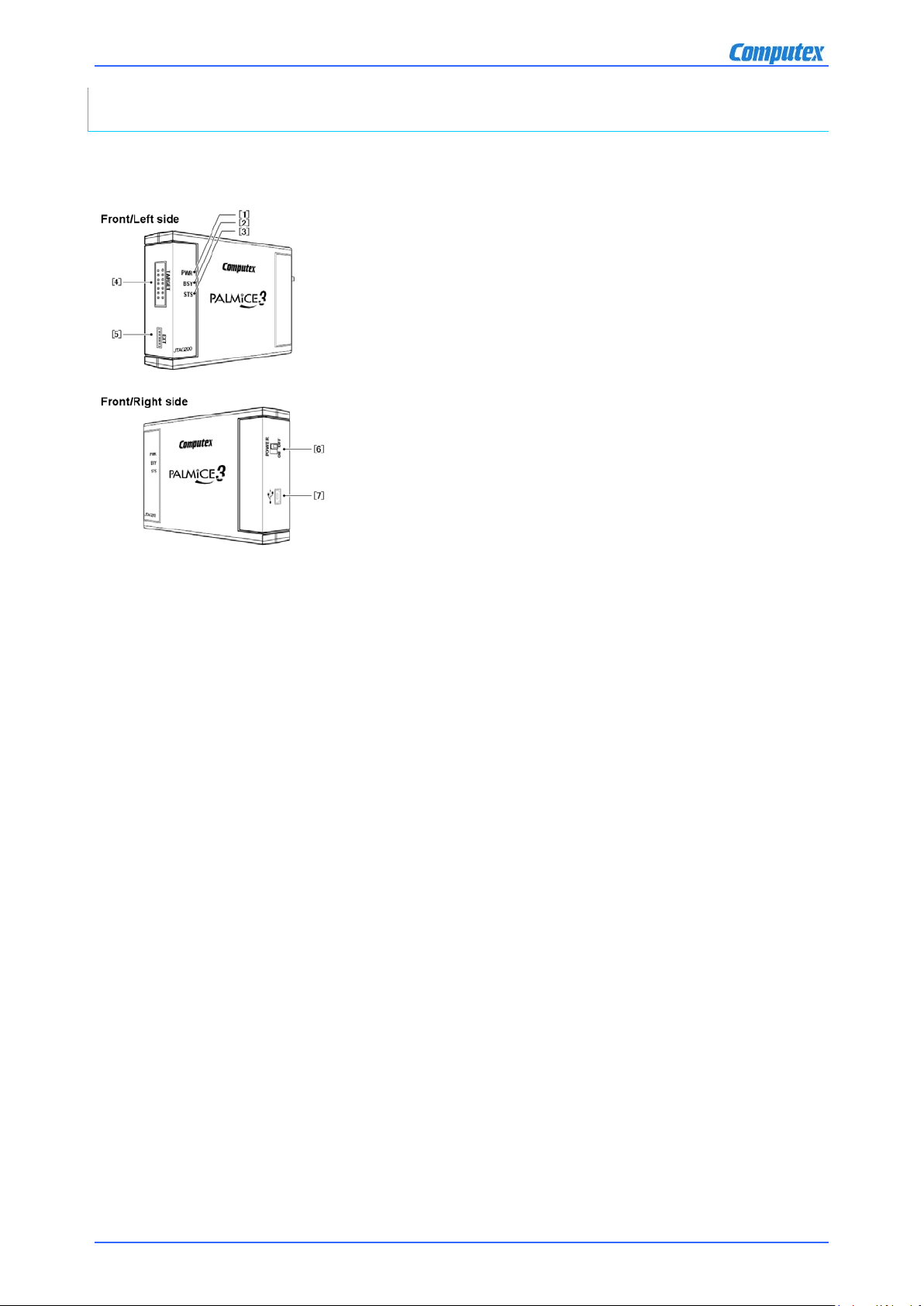
Appearance drawing of PALMiCE3 JTAG200 model is given to the following.
[1] PWR LED
Comes on when the power is supplied to PALMiCE3. Power is supplied from
the host computer through USB cable.
[2] BSY LED
Flickers during communication between PALMiCE3 and the target CPU.
[3] STS LED
Lit normally during user program execution.
Also, flashes in some cases to notify errors.
For details, refer to the user's manual.
[4] TARGET connector
20-pin connector for connecting PALMiCE3 to the target system.
[5] EXT
[6] Power switch
Turns ON/OFF the PALMiCE3’s power. Power input state can be checked with [1] POWER LED.
[7] USB connector
Connect USB cable (mini-B type).
PALMiCE3 JTAG200 model Hardware Manual Chapter 2 PALMiCE3 JTAG200 Hardware Specifications 5
Page 25
2.3.1
Hardware revision
How revision sticker reads
A
B C D E F
G H I
J K L
A B C D E F G H I J K
L
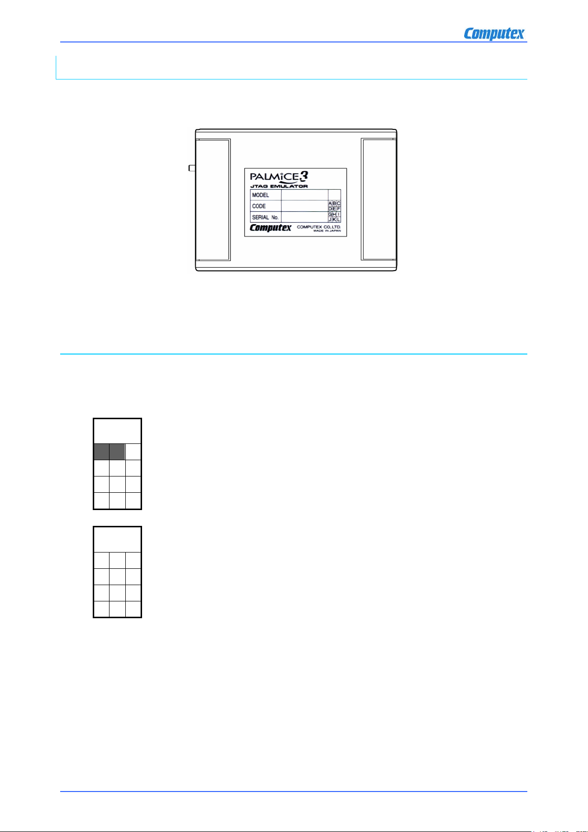
The sticker with PALMiCE3 information is placed at the back of PALMiCE3 main unit.
Back side of PALMiCE3 main unit
Read the number given on the upper side and the last alphabet shaded with black.
Example 1): Hardware revision 1-B
1
Example 2): Hardware revision 2-0
2
In Example 1), PALMiCE3 hardware revision reads as 1-B.
In Example 2), where alphabets are not shaded, PALMiCE3 hardware revision
reads as 2-0.
PALMiCE3 JTAG200 model Hardware Manual Chapter 2 PALMiCE3 JTAG200 Hardware Specifications 6
Page 26
2.4
External probe
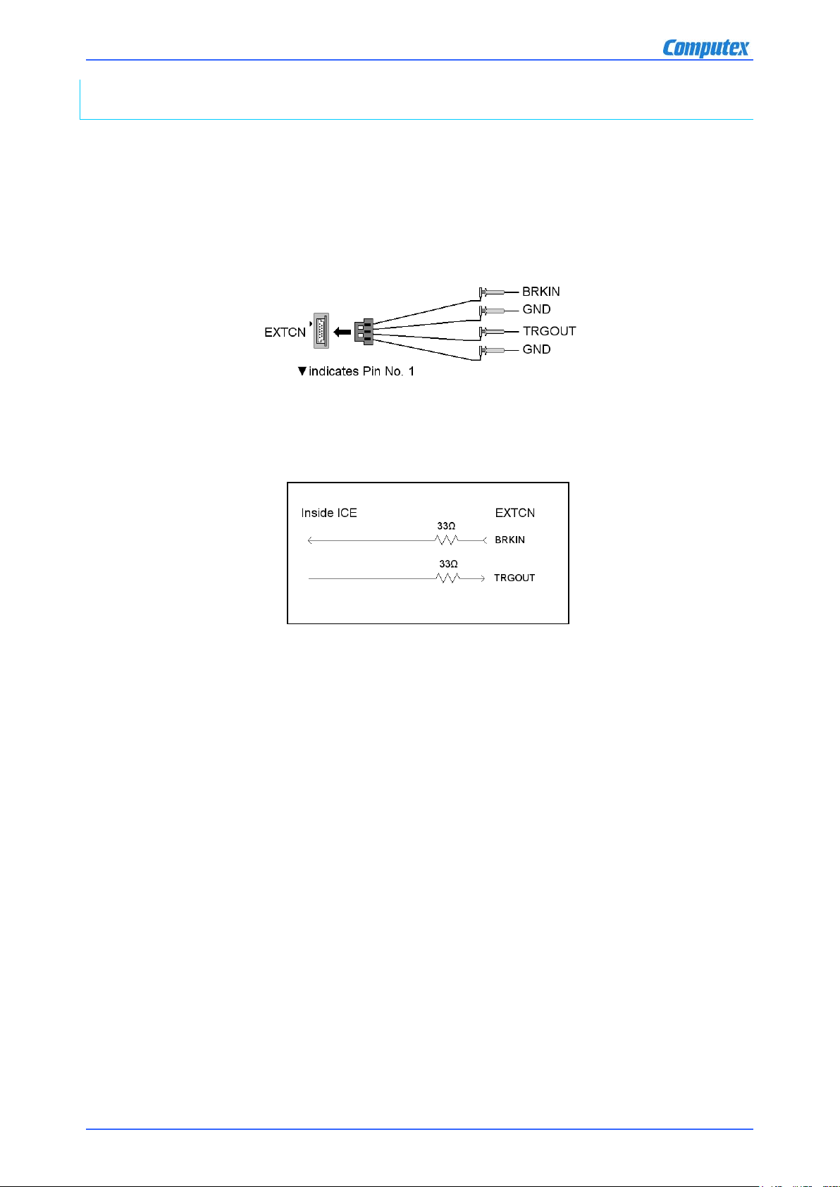
External probe is to be used when synchronizing CSIDE with the target system.
BRKIN input is used to break the user program with an arbitrary external signal. This is an optional signal and can be left
unconnected if not used.
Note that the TRGOUT signal is not used in case of PALMiCE3 JTAG200.
Connect the exernal probe to EXTCN of PALMiCE3.
The target interface has the following circuit.
LVTTL level is accepted for input. Never apply voltage over absolute maximum rating - 0.5V-3.6V of IC, or will lead to
malfunction.
PALMiCE3 JTAG200 model Hardware Manual Chapter 2 PALMiCE3 JTAG200 Hardware Specifications 7
Page 27
Chapter 3
Target Interface Specifications
3.1
Introduction
3.2
Target interface
3.2.1
Shape of the connector for debugger
documentations provided by manufacturers.)
3.2.2
Dimension of the target cable
documentations provided by manufacturers.)
3.2.3
Specifications of target interface signals
VIL
Target voltage ÷ 2 – 0.35
VIH
Target voltage ÷ 2 + 0.35
Output voltage level
VOL
Under 0.2V
This Chapter spells out target interface specifications for connecting PALMiCE3 JTAG200 to the target system.
The interface for connecting PALMiCE3 JTAG200 to the target system is described.
Target interface varies from CPU to CPU.
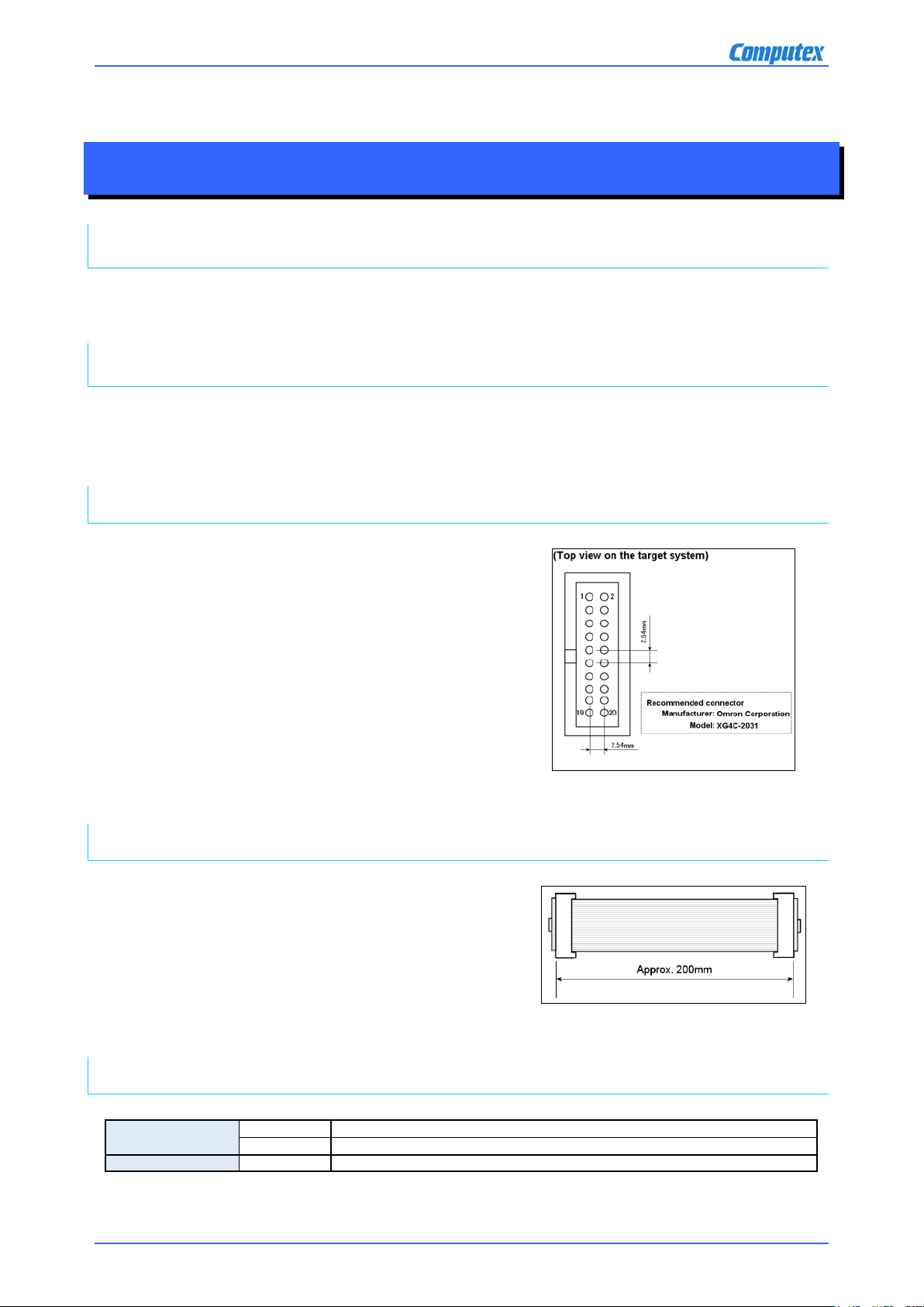
The shape of the debugger connector (20-pin MIL connector) that is
usually mounted on the target system is shown here.
The dimension of target cable for connecting PALMiCE3 JTAG200 to
the target system is shown here.
Input voltage level
(For detailed dimensions of the connector, refer to the
(For detailed dimensions of the connector, refer to the
PALMiCE3 JTAG200 model Hardware Manual Chapter 3 Target Interface Specifications 8
Page 28
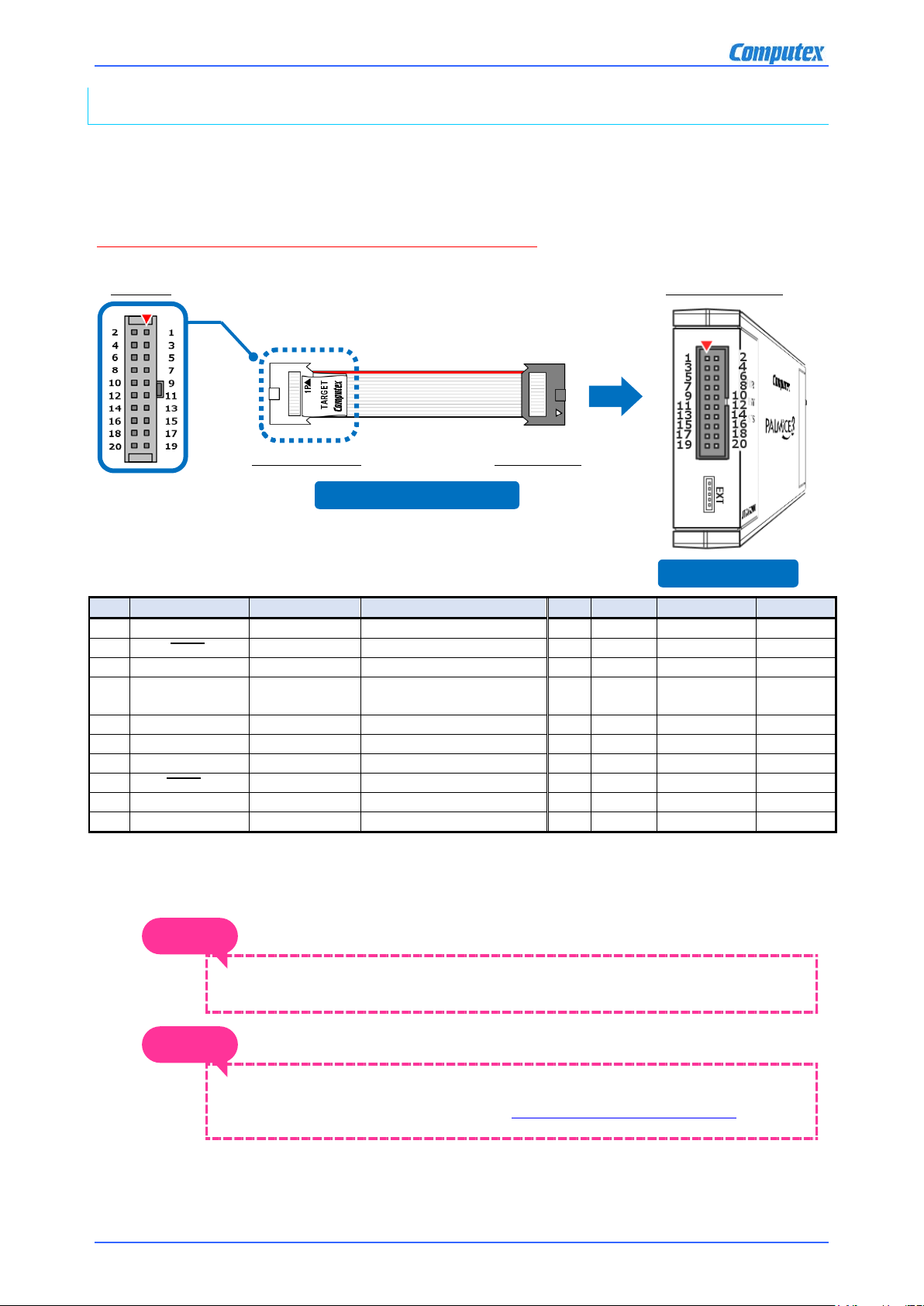
3.2.4
The target interface on PALMiCE3 side
No.
Signal
Input/Output
Remarks
No.
Signal
Input/Output
Remarks 1 VTref*1
Output
550KΩ Pul l-down
2
TVDD
Output
Not used 3 TRST
Input
100Ω Series
4
GND
5
TDI(N.C.
)
Input
33Ω Series 10KΩ Pull-up*2
6
GND
(Input/Output
)
9
TCK(SWCLK
)
Input
33Ω Series
10
GND
11
RTCK(N.C.
)
Output
33Ω Series 100KΩ Pu ll-down
12
GND
13
TDO(SWO
)
Output
33Ω Series 10KΩ Pull-up*2
14
GND
15
SRST*3
Input
100Ω Series Open-collector
16
GND
17
DBGRQ(N.C.
)
Input
33Ω Series
18
GND
19
DBGACK(N.C.
)
Output
33Ω Series 100KΩ Pu ll-down
20
GND
Target system side
PALMiCE3 side
Connector
PALMiCE3 side view
Connecto to
Target cable
PALMiCE3
NOTE
NOTE
The target interface on PALMiCE3 side is described.
The terminal/pin numbers and the target cable are specific to PALMiCE3.
Make sure only to use the product cable supplied with the product.
PALMiCE3
*4
7 TMS(SWDIO*4)
*4
*4
*4
*4
*4
*1 : For VTref pin, connect the signal to the power at the same voltage level as the target interface. VTref pin is to serve for potential detection,
and pull-up signal of 1KΩ will do.
*2 : Each of these signals has been pulled up to the voltage level detected from VTref pin.
*3 : It is an output signal with open-collector specification from PALMiCE3. Pull it up at a few KΩ (10KΩ recommended) on the target side.
*4 : Names of signals in ( ) are those for the time of Serial Wire Debugging. N.C. indicates that the pin is not used.
Input
33Ω Series 10KΩ Pull-up*2 8 GND
*4
Each name of the signal varies depending on the CPU you use.
For Target connection reference diagram, refer to "PALMiCE3 Technical
Information" up on Computex website ( http://www.computex.co.jp/eg/ ).
PALMiCE3 JTAG200 model Hardware Manual Chapter 3 Target Interface Specifications 9
Page 29

E-mail: [email protected]
CM951(F)1810
Computex Co., Ltd.
Head Office
Tairanbo Bldg.,
4-432-13 Gojobashi-Higashi, Higashi yama-ku, KYOTO 6050846 Japan
Sales Department
PALMiCE3 JTAG200 model Hardware Manual
Oct. 2018 Sixth
Edition
 Loading...