

Page 1

CM-T43
Reference Guide
Page 2
Legal
© 2016 Compulab Ltd.
All Rights Reserved. No part of this document may be photocopied, reproduced, stored in a
retrieval system, or transmitted, in any form or by any means whether, electronic, mechanical, or
otherwise without the prior written permission of Compulab Ltd.
No warranty of accuracy is given concerning the contents of the information contained in this
publication. To the extent permitted by law no liability (including liability to any person by
reason of negligence) will be accepted by Compulab Ltd., its subsidiaries or employees for any
direct or indirect loss or damage caused by omissions from or inaccuracies in this document.
Compulab Ltd. reserves the right to change details in this publication without notice.
Product and company names herein may be the trademarks of their respective owners.
Compulab Ltd.
P.O. Box 687 Yokneam Illit
20692 ISRAEL
Tel: +972 (4) 8290100
http://www.compulab.co.il
Fax: +972 (4) 8325251
Revised September 2017 CM-T43 Reference Guide 2
Page 3
Table of Contents
Table of Contents
1 INTRODUCTION .......................................................................................................... 6
1.1 About This Document .................................................................................................. 6
1.2 CM-T43 Part Number Legend ..................................................................................... 6
1.3 Related Documents ...................................................................................................... 6
2 OVERVIEW ................................................................................................................... 7
2.1 Highlights .................................................................................................................... 7
2.2 Block Diagram ............................................................................................................. 8
2.3 CM-T43 Features ......................................................................................................... 9
3 CORE SYSTEM COMPONENTS ............................................................................. 11
3.1 Sitara AM437x SoC ................................................................................................... 11
3.2 PRU-ICSS .................................................................................................................. 12
3.3 Multimedia System .................................................................................................... 13
3.4 Memory ...................................................................................................................... 13
3.4.1 DRAM .............................................................................................................. 13
3.4.2 Primary Storage (Boot-loader) ......................................................................... 13
3.4.3 Secondary Storage (OS & User data) ............................................................... 13
4 PERIPHERAL INTERFACES ................................................................................... 14
4.1 Display Interface ........................................................................................................ 16
4.2 Camera Interfaces (VPFE) ......................................................................................... 18
4.3 Local Bus (GPMC) .................................................................................................... 19
4.4 Analog Audio ............................................................................................................. 23
4.5 Digital Audio (McASP) ............................................................................................. 24
4.6 WLAN, Bluetooth and NFC ...................................................................................... 26
4.7 Ethernet ...................................................................................................................... 27
4.8 USB2.0....................................................................................................................... 28
4.9 MMC / SD / SDIO ..................................................................................................... 29
4.10 UART .................................................................................................................... 32
4.11 I2C ......................................................................................................................... 34
4.12 SPI ......................................................................................................................... 35
4.13 Quad SPI (QSPI) ................................................................................................... 36
4.14 CAN Bus ............................................................................................................... 37
4.15 ADC and Resistive Touch-Screen ........................................................................ 38
4.16 HDQ / 1-Wire........................................................................................................ 39
4.17 GPIO ..................................................................................................................... 39
4.18 Enhanced Capture module (eCAP) ....................................................................... 45
4.19 Enhanced PWM module (eHRPWM) ................................................................... 46
4.20 Quadrature Encoder Pulse module (eQEP) ........................................................... 48
4.21 PRU-ICSS ............................................................................................................. 50
4.21.1 PRU-ICSS MII ................................................................................................. 50
4.21.2 PRU-ICSS UART ............................................................................................. 52
Revised September 2017 CM-T43 Reference Guide 3
Page 4
Table of Contents
4.21.3 PRU-ICSS Industrial Ethernet Peripheral ........................................................ 52
4.21.4 PRU-ICSS Industrial Capture interface (PRU-ICSS1 eCAP) .......................... 53
4.21.5 PRU-ICSS GPI / GPO ...................................................................................... 54
4.22 Timers ................................................................................................................... 57
4.23 General Purpose Clocks ........................................................................................ 57
4.24 External DMA/Interrupt requests.......................................................................... 58
5 SYSTEM LOGIC ......................................................................................................... 59
5.1 Power Supply ............................................................................................................. 59
5.2 Power Management ................................................................................................... 59
5.3 Reset .......................................................................................................................... 59
5.4 Boot Sequence ........................................................................................................... 60
5.5 Signal Multiplexing Characteristics .......................................................................... 61
5.6 Flash Write-protection ............................................................................................... 65
5.7 RTC ............................................................................................................................ 65
5.8 LED ............................................................................................................................ 65
6 CARRIER BOARD INTERFACE ............................................................................. 66
6.1 Connector Pinout ....................................................................................................... 66
6.2 Mating Connectors ..................................................................................................... 75
6.3 Mechanical Drawings ................................................................................................ 76
6.4 Standoffs/Spacers ...................................................................................................... 77
7 OPERATIONAL CHARACTERISTICS .................................................................. 78
7.1 Absolute Maximum Ratings ...................................................................................... 78
7.2 Recommended Operating Conditions ........................................................................ 78
7.3 DC Electrical Characteristics ..................................................................................... 78
7.4 ESD Performance ...................................................................................................... 78
7.5 Operating Temperature Ranges ................................................................................. 78
8 APPLICATION NOTES ............................................................................................. 79
8.1 Carrier Board Design Guidelines ............................................................................... 79
8.2 Carrier Board Troubleshooting .................................................................................. 79
8.3 Ethernet Magnetics Implementation .......................................................................... 80
8.3.1 Magnetics Selection .......................................................................................... 80
8.3.2 Magnetics Connection ...................................................................................... 80
Revised September 2017 CM-T43 Reference Guide 4
Page 5
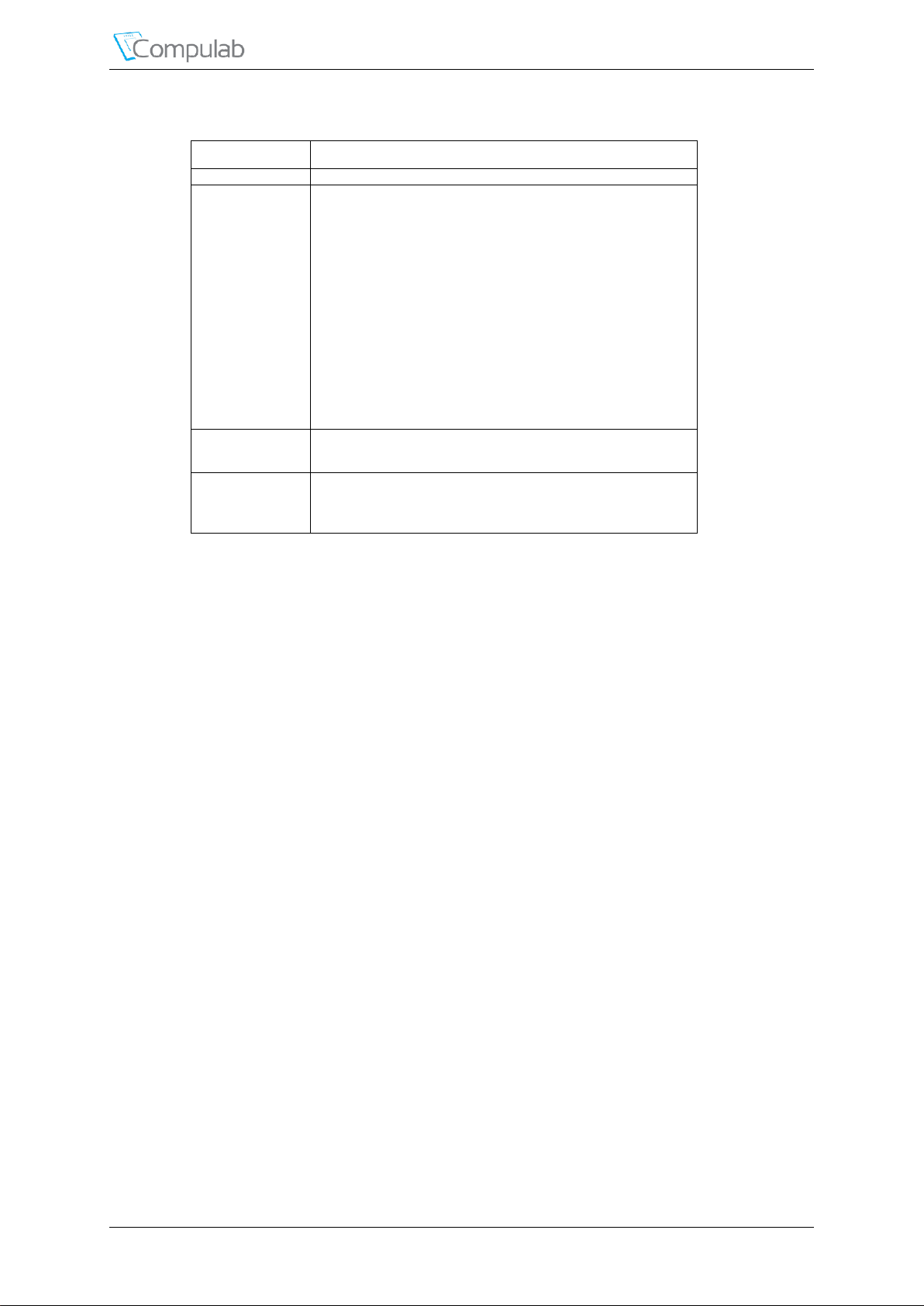
Revision Notes
Date
Description
Dec 2015
First release
Jan 2016
Bugfix release:
Updated company logo and document layout.
Added notes and revised signals tables for all signals on the following
CM-T43 pins (across the whole document): 4, 16, 30, 32, 34, 36, 38,
39, 40, 41, 42, 43, 44, 47, 48, 50, 51, 57, 59, 100, 102, 104, 106, 108,
110, 112, 116, 117, 118, 120, 122, 124, 126, 128, 130, 133, 134, 136,
138, 140, 149, 151, 153, 155, 161, 163, 192, 202.
Revised note in chapter 5.6
Revised pinout table for better readability
Revised spacers information (chapter 6.4)
Attached excel pinout table into this document
Fixed pin# of signal RTC_WAKEUP in table 62 to pin # 179
Added a new chapter describing EEPROM/SPI-Flash write protection
feature.
Aug 2016
Documented the effect of ‘N16G’ (16GB onboard eMMC storage) option
on signals availability throughout chapters 4, 5 and the attached pinmux
excel table.
Aug 2017
Updated links for related documents in table 2.
Updated MTTF specifications in table 4.
Updated functionality description for pin 181 in section 5.2.
Table 1 Revision Notes
Please check for a newer revision of this manual at the CompuLab web site
http://www.compulab.co.il/. Compare the revision notes of the updated manual from the web site
with those of the printed or electronic version you have.
Revised September 2017 CM-T43 Reference Guide 5
Page 6
Introduction
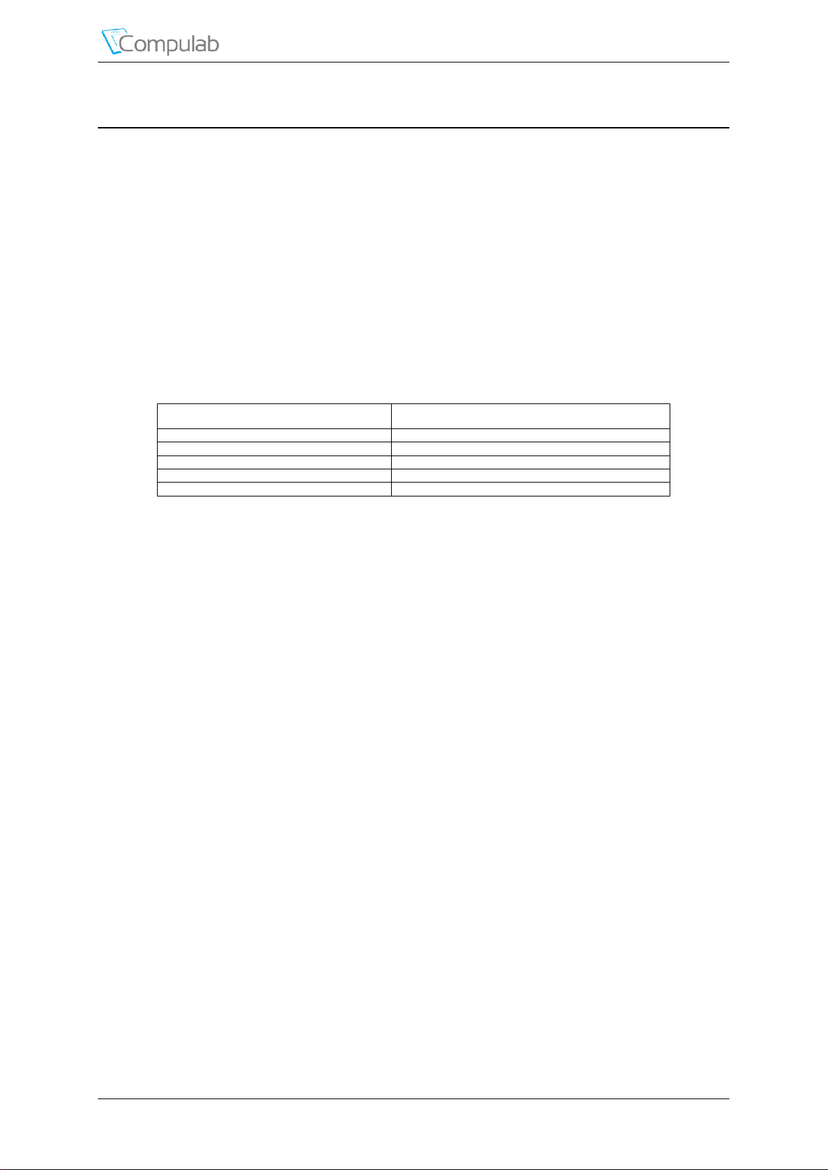
Document
Location
CM-T43 Developer Resources
http://www.compulab.com/
Sitara AM437x Reference Manual
http://www.ti.com/product/AM4377/technicaldocuments
Sitara AM437x Datasheet
http://www.ti.com/product/AM4377/technicaldocuments
1 INTRODUCTION
1.1 About This Document
This document is part of a set of reference documents providing information necessary to operate
and program CompuLab CM-T43 Computer-on-Module.
1.2 CM-T43 Part Number Legend
Please refer to the CompuLab website ‘Ordering information’ section to decode the CM-T43 part
number: http://www.compulab.co.il/products/computer-on-modules/cm-t43/#ordering.
1.3 Related Documents
For additional information, refer to the documents listed in Table 2.
Table 2 Related Documents
Revised September 2017 CM-T43 Reference Guide 6
Page 7
Overview
2 OVERVIEW
2.1 Highlights
Texas Instruments Sitara AM437x ARM Cortex-A9 processor @ up to 1.0GHz
NEON™ SIMD Coprocessor and Vector – Interrupt Controller Floating Point (VFPv3)
Programmable Real-Time Unit Subsystem and Industrial Communication Subsystem
(PRU-ICSS).
Up to 1GB DDR3
Up to 32GB on-board eMMC or raw SLC NAND storage
SGX530 Graphics Engine
1Gbit Ethernet × 2, USB2.0 Host/Device × 1, USB2.0 Host ×1, UART × 6, SDIO × 3,
ADC × 16, CAN bus × 2, Onboard WiFi IEEE 802.11a/b/g/n/ac, Onboard Bluetooth 4.0
(supports Low Energy), Onboard NFC.
Miniature size: 36 × 68 x 5 mm
SB-SOM-T43 carrier board turns the CM-T43 system on module (CoM/SoM) into SBC-
T43, a single board computer
Revised September 2017 CM-T43 Reference Guide 7
Page 8
Overview
Texas
Instruments
AM437x
SPI0
USB2.0
DDR3
Memory
Controller
SPI Flash
(primary
bootloader
storage)
Wolfson Audio
Codec
I2C
EEPROM
(board info)
DDR3
(Up to 1GB)
32bit
ARM
Cortex-A9
TPS65218
PMIC
Marvell
88W8897 Based
WLAN+BT+NFC
Stereo
M
ultifunctio
nal sig
nals (m
uxed)
2 Ethernet Ports
(1Gbps)
Local bus
3 x I2C
2 x McASP
Parallel 24bit
Display
6 x UART
5 x McSPI
2 x VPFE
3D
acceleration
(SGX530)
1 x 1-WIRE
3 x SD/SDIO
2
04-pin
S
O
D
IM
M
edg
e co
nnector
6 x Timers/PWM
McASP0
I2C0
Optional Bypass
USB2.0 OTG
USB2.0 Host
1Gbit PHY
1Gbit PHY
RGMII1
RGMII2
1Gbit Eth
1Gbit Eth
MMC2
Optional Bypass
8x General Purpose ADC / Resistive Touch
8x General Purpose ADC
Backup Battery Power
2 x CAN
133 x GPIO
1 x QuadSPI
3 x eCAP
6 x eHRPWM
3 x eQEP
PRU GPIO
1 x PRU UART
1 x PRU eCAP
Cryptographic
Engine
Integrated
Ethernet
switch
1 x JTAG
TestPoints
JTAG
Optional Bypass
Optional Bypass
Local bus (GPMC)
Power
Power
Power
up to 1x Parallel Display (24bit max)
up to 1x Remote Frame Buffer
up-to 3x Capture interfaces (eCAP)
up-to 6x PWM interfaces (eHRPWM)
up-to 6x Timer/PWM interfaces
up-to 3x Quadrature encoder
up to 2x Camera (VPFE)
up-to 4x SPI
up-to 6x UART
up-to 2x I2C Bus
up-to 2x I2S/McASP
up-to 133x GPIOs
up-to 3x SD/SDIO/MMC (1/4/8-bit)
up-to 1x HDQ/SIO 1-wire
up-to 2x CAN bus
up-to 1x Quad SPI
MMC1
SLC NAND Flash
(128MB - 512MB)
or
eMMC
(4GB - 32GB)
ADC0
USB2.0
ADC1
RTC
Stereo
Microphone
up-to 1x PRU-ICSS1 UART
up-to 1x PRU-ICSS1 eCAP
up-to 6x Industrial Ethernet digital outputs
up-to 8x Industrial Ethernet digital inputs
up-to 2x PRU-ICSS1 MII (ethernet)
up-to 13x PRU-ICSS1 GPI
up-to 12x PRU-ICSS1 GPO
up-to 40x PRU-ICSS0 GPIO
Two
PRU-ICSS
cores
PRU MII
PRU Industrial
Ethernet
Optional Bypass
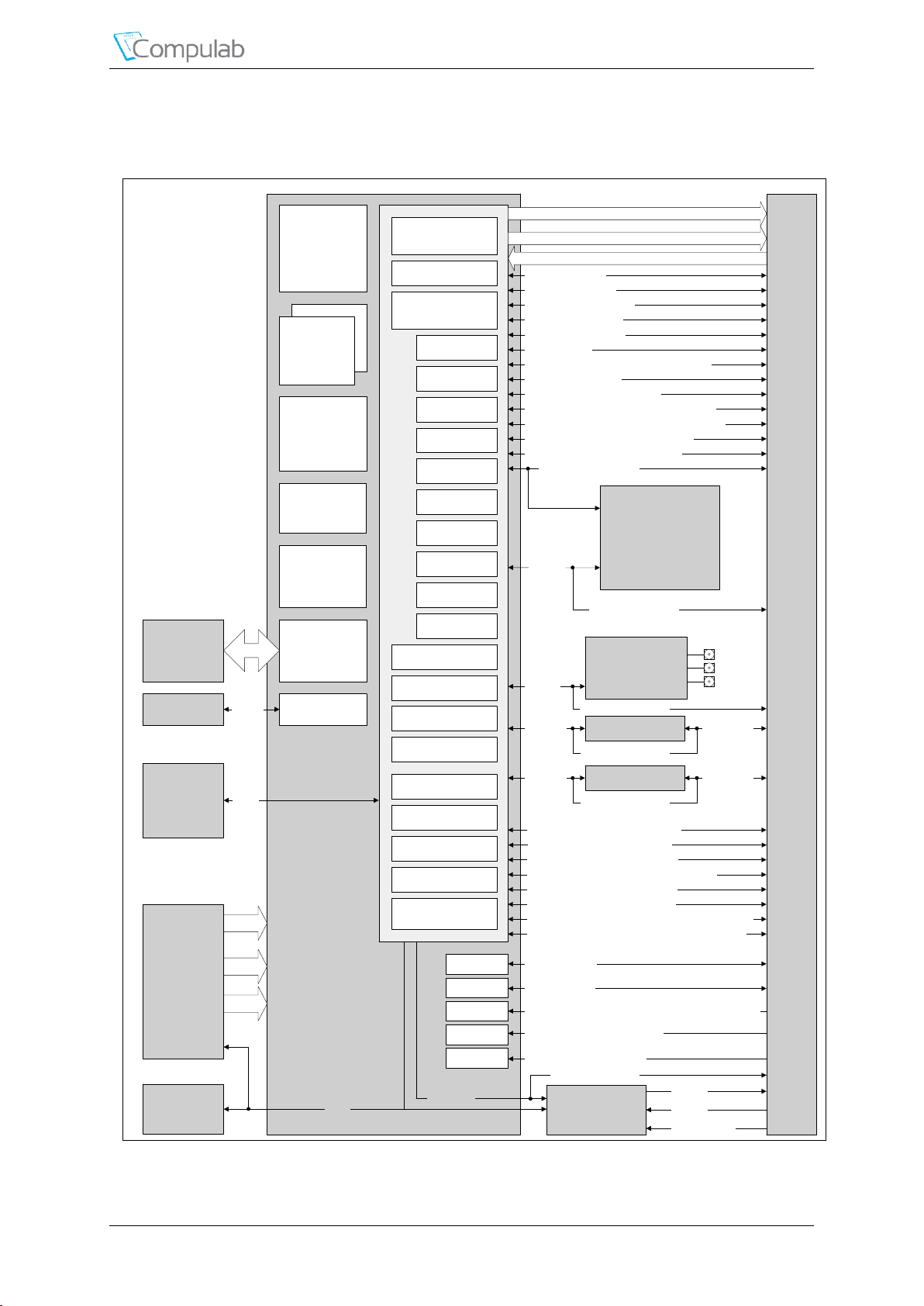
2.2 Block Diagram
Figure 1 CM-T43 Block Diagram
Revised September 2017 CM-T43 Reference Guide 8
Page 9
Overview
Feature
Description
Option
CPU Core and Graphics
CPU
Texas Instruments Sitara AM4379 ARM Cortex-A9, 1GHz
NEON™ SIMD and VFPv3
C1000M
Texas Instruments Sitara AM4376 ARM Cortex-A9, 800MHz
NEON™ SIMD and VFPv3
C800
Graphics
Acceleration Unit
PowerVR SGX530 GPU supporting Direct3D Mobile, OpenGL-ES 2.0
and OpenVG 1.0
C1000M
Real-Time
Coprocessor
Programmable Real-Time Unit Subsystem supporting 1588, BiSS,
EnDat 2.2, EtherCAT, EtherNet/IP, Ethernet POWERLINK,
HIPERFACE DSL, PROFIBUS, PROFINET RT/IRT, SERCOS III and
Sigma Delta Filter protocols
C1000M
Programmable Real-Time Unit Subsystem supporting 1588, BiSS,
EnDat 2.2, EtherNet/IP, HIPERFACE DSL, PROFIBUS, PROFINET
RT/IRT, SERCOS III and Sigma Delta Filter protocols
C800
Memory and Storage
RAM
128MB – 1GB, DDR3-800, 32-bit data bus
D
Storage
On-board SLC NAND flash, 128MB - 512MB
N
On-board eMMC flash, 4GB - 32GB
Display and Camera
Display
Parallel 24-bit display interface - up to 100 Mpixels/sec
+
Remote frame buffer interface
+
Touchscreen
On-board 4/5/8-wire resistive touch-screen controller
+
Capacitive touch-screen support through SPI and I2C interfaces
+
Camera
Primary 12-bit parallel camera (VPFE) interface
+
Secondary 12-bit parallel camera (VPFE) interface
not WB
Network
Gigabit Ethernet
Primary 1000/100/10Mbps Ethernet port (MAC+PHY)
E1
Secondary 1000/100/10Mbps Ethernet port (MAC+PHY)
E2
WiFi
Dual-band, dual-antenna 2x2 MIMO 802.11ac/a/b/g/n WiFi interface
WB
Bluetooth
Bluetooth 4.0 (low energy)
WB
NFC
NFC - full protocol support for ISO 14443A/B, ISO 18092 and ISO
15693
WB
Audio
Analog Audio
Audio codec with analog stereo output, stereo input and electret
microphone support
A
Digital Audio
I2S compliant digital audio interface
not A
I/O
Local Bus
External local bus interface, variable rate up to 100 MHz, up-to 16-bit
+
USB
USB2.0 high-speed dual-role (host / device) port
+
USB2.0 high-speed host port
+
Serial Ports (UARTs)
Up to 6 UART ports, 16C750 compatible, 3.3V interface, up to 3.6
Mbps
+
CAN bus
Up to 2 CAN bus interfaces, 3.3V levels
+
MMC/SD/SDIO
Up to 3 MMC/SD/SDIO interfaces
+
SPI
Up to 4 SPI bus interfaces
+
I2C
Up to 2 I2C interfaces
+
1-Wire
1-Wire interface
+
GPIO
Up to 133 multifunction signals. Can be used as GPIO (shared with other
functions)
+
ADC
Up to 16 general-purpose ADC channels
+
System Logic
RTC
Real time clock, powered by external lithium battery
+
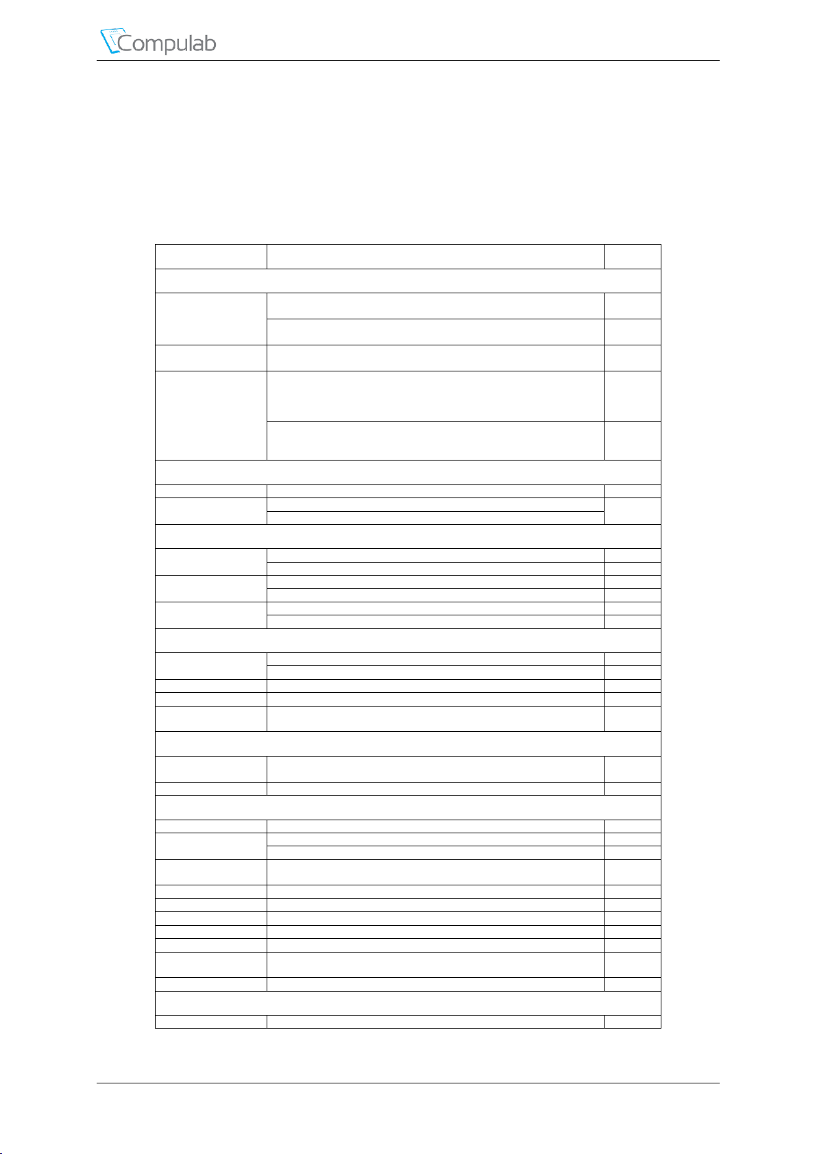
2.3 CM-T43 Features
The "Option" column specifies the CoM/SoM configuration option required to have the particular
feature. When a CoM/SoM configuration option is prefixed by “NOT”, the particular feature is
only available when the option is not used. A feature is only available when a CoM/SoM
configuration complies with all options denoted in the “Option” column.
"+" means that the feature is always available.
Table 3 Features and Configuration options
Revised September 2017 CM-T43 Reference Guide 9
Page 10
Overview
Electrical Specifications
Supply Voltage
3.3V - 5.0V typ
Digital I/O voltage
3.3V
Active power consumption
TBD
Mechanical Specifications
Dimensions
36 × 68 x 5 mm
Weight
12 gram
Connectors
SODIMM-204
Environmental and Reliability
MTTF
> 200,000 hours
Operation temperature (case)
Commercial: 0° to 70° C
Extended: -20° to 70° C
Industrial: -40° to 85° C. Click for availability note
Storage temperature
-40° to 85° C
Relative humidity
10% to 90% (operation)
05% to 95% (storage)
Shock
50G / 20 ms
Vibration
20G / 0 - 600 Hz
Table 4 Electrical, Mechanical and Environmental Specifications
Revised September 2017 CM-T43 Reference Guide 10
Page 11
Core system components
3 CORE SYSTEM COMPONENTS
3.1 Sitara AM437x SoC
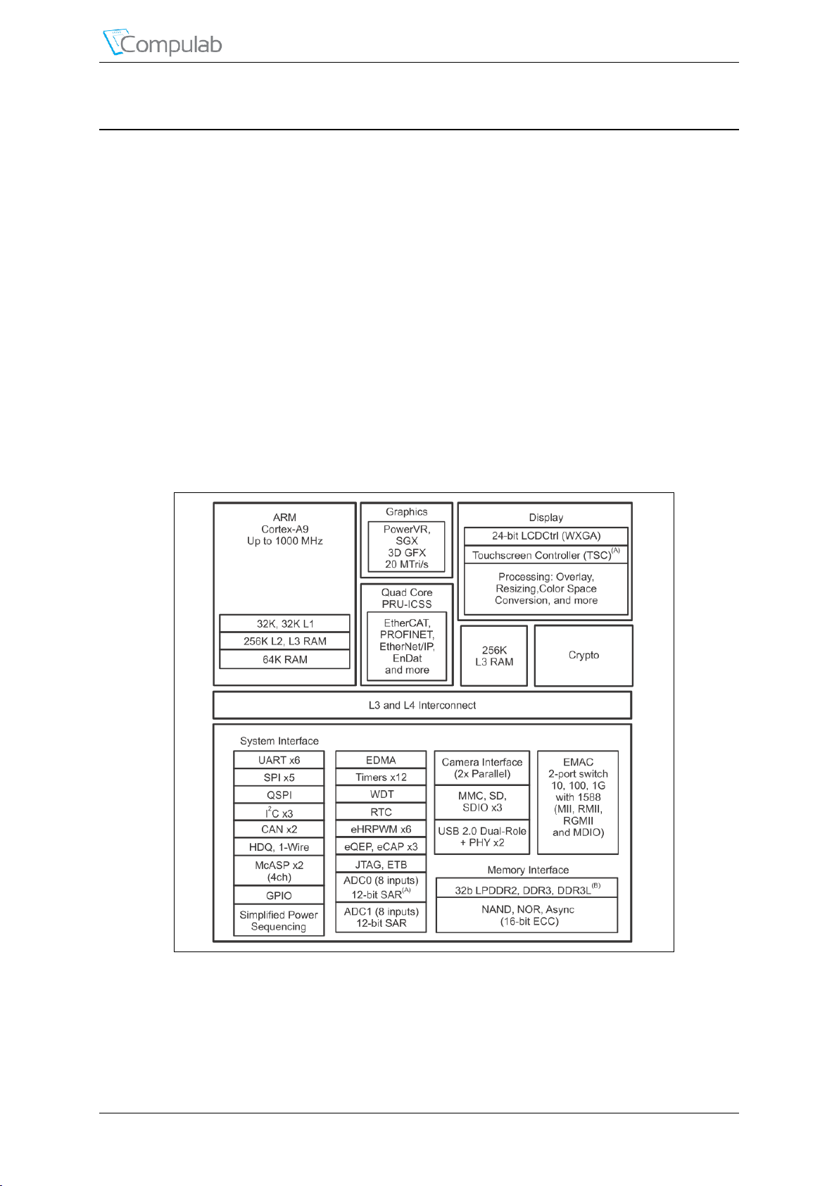
The TI Sitara AM437x high-performance system-on-chip (SoC) is built around the ARM CortexA9 core. The SoC includes POWERVR SGX™ 3D graphics acceleration for rich graphical user
interfaces, as well as a co-processor for deterministic, real-time processing including industrial
communication protocols, such as EtherCAT®, PROFIBUS®, EnDat and others. Cryptographic
acceleration is also available in every CM-T43 device. Secure boot can also be made available for
anti-cloning and illegal software update protection.
Up to 1000-MHz Sitara™ ARM® Cortex®-A9 32-Bit RISC processor
NEON™ SIMD Coprocessor and Vector Floating Point (VFPv3) Coprocessor
32KB of Both L1 Instruction and Data Cache
256KB of L2 Cache or L3 RAM
SGX530 Graphics Engine
Crypto Hardware Accelerators (AES, SHA, RNG, DES and 3DES)
Programmable Real-Time Unit Subsystem and Industrial Communication Subsystem
(PRU-ICSS)
Figure 2 SITARA AM437X Block Diagram
Revised September 2017 CM-T43 Reference Guide 11
Page 12
Core system components
3.2 PRU-ICSS
The programmable real-time unit subsystem and industrial communication subsystem (PRUICSS) is separate from the ARM core and allows independent operation and clocking for greater
efficiency and flexibility. The PRU-ICSS enables additional peripheral interfaces and real-time
protocols such as EtherCAT, PROFINET, EtherNet/IP, PROFIBUS, Ethernet Powerlink, Sercos,
EnDat, and others. The PRU-ICSS enables EnDat and another industrial communication protocol
in parallel.
The PRU-ICSS consists of dual 32-bit RISC cores (Programmable Real-Time Units, or PRUs),
shared, data, and instruction memories, internal peripheral modules, and an interrupt controller
(INTC). The programmable nature of the PRU-ICSS, along with their access to pins, events and
all SoC resources, provides flexibility in implementing fast real-time responses, specialized data
handling operations, custom peripheral interfaces, and in offloading tasks from the other processor
cores of the SoC. Sitara AM437x contains two subsystems: PRU-ICSS1 and PRU-ICSS0. PRUICSS1 is considered a superset of PRU-ICSS0.
The PRU cores within the subsystems have access to all resources on the SoC through the
Interface/OCP Master port, and the external host processors can access the PRU-ICSS resources
through the Interface/OCP Slave port. The 32-bit interconnect bus connects the various internal
and external masters to the resources inside the PRU-ICSS. The INTC handles system input
events and posts events back to the device-level host CPU.
The PRU cores are programmed with a small, deterministic instruction set. Each PRU can operate
independently or in coordination with each other and can also work in coordination with the
device-level host CPU. This interaction between processors is determined by the nature of the
firmware loaded into the PRU's instruction memories
The PRU is a processor optimized for performing embedded tasks that require manipulation of
packed memory mapped data structures, handling of system events that have tight real-time
constraints and interfacing with systems external to the SoC. The PRU is both very small and very
efficient at handling such tasks
Supports Protocols such as EtherCAT®, PROFIBUS, PROFINET, and EtherNet/IP™,
EnDat 2.2, and More
Two Programmable Real-Time Units (PRUs) Subsystems With Two PRU Cores Each
Each Core is a 32-Bit Load and Store RISC Processor Capable of Running at 200
MHz
12KB (PRU-ICSS1), 4KB (PRU-ICSS0) of Instruction RAM with Single-Error
Detection (Parity)
8KB (PRU-ICSS1), 4KB (PRU-ICSS0) of Data RAM with Single-Error Detection
(Parity)
Single-Cycle 32-Bit Multiplier with 64-Bit Accumulator
Enhanced GPIO Module Provides Shift-In and Shift-Out Support and Parallel Latch
on External Signal
12KB (PRU-ICSS1 only) of Shared RAM with Single-Error Detection (Parity)
Three 120-Byte Register Banks Accessible by Each PRU
Interrupt Controller Module (INTC) for Handling System Input Events
Local Interconnect Bus for Connecting Internal and External Masters to the Resources
Inside the PRU-ICSS
Peripherals Inside the PRU-ICSS:
One UART Port with Flow Control Pins, Supports Up to 12 Mbps
One Enhanced Capture (eCAP) Module
Two MII Ethernet Ports that Support Industrial Ethernet, such as EtherCAT
One MDIO Port
Industrial Communication is Supported by Two PRU-ICSS Subsystems
Revised September 2017 CM-T43 Reference Guide 12
Page 13
Core system components
3.3 Multimedia System
CM-T43 multimedia capabilities are derived from the 2D/3D graphics accelerator (SGX)
subsystem of the Sitara AM437x SoC. The SGX subsystem can accelerate 2-dimensional (2D)
and 3-dimensional (3D) graphics applications. The subsystem is based on the POWERVR ® SGX
core from Imagination Technologies. SGX is a new generation of programmable POWERVR
graphic cores. The POWERVR ® SGX Main Features include the following:
2D and 3D graphics
Tile-based architecture
Universal scalable shader engine (USSE™) – multithreaded engine incorporating pixel
and vertex shader functionality
Advanced shader feature set: in excess of OpenGL2.0
Industry-standard API support: OpenGL ES 1.1 and 2.0, OpenVG v1.0.1
Fine-grained task switching, load balancing, and power management
Advanced geometry direct memory access (DMA) driven operation for minimum CPU
interaction
Programmable high-quality image anti-aliasing
Built in MMU
Fully virtualized memory addressing for OS operation in a unified memory architecture
Advanced and standard 2D operations [e.g., vector graphics, BLTs (block level transfers),
ROPs (raster operations)]
3.4 Memory
3.4.1 DRAM
CM-T43 is equipped with up to 1GB of onboard DDR3 memory. The DDR3 data bus is 32-bits
wide and operates at 400 MHz clock frequency (DDR3-800).
NOTE: CM-T43 boards with 128MB of DRAM (D128 option) feature a 16-bit wide DDR3
data bus.
3.4.2 Primary Storage (Boot-loader)
The CM-T43 is assembled with 2MBytes of SPI NOR flash. The SPI NOR flash is the primary
non-volatile memory device of CM-T43, used for the boot-loader and configuration blocks
storage.
3.4.3 Secondary Storage (OS & User data)
CM-T43 is available with optional secondary on-board storage designed to store the operating
system and user data. One of the following on-board non-volatile memory devices can be used as
the secondary on-board storage.
On-board eMMC flash (up to 32GBytes).
On-board raw SLC NAND Flash (up to 1GBytes).
The secondary storage device is designed to store the operating system (kernel & root filesystem)
and general purpose (user) data.
Revised September 2017 CM-T43 Reference Guide 13
Page 14
Peripheral Interfaces
4 PERIPHERAL INTERFACES
CM-T43 implements a variety of peripheral interfaces through the SODIMM-204 carrier board
connector. The following notes apply to interfaces available through the SODIMM-204 interface:
Some interfaces/signals are available only with/without certain configuration options of CM-
T43. The availability restrictions of each signal are described in the “Signals description”
table for each interface.
Many of the CM-T43 carrier board interface pins are multifunctional. Up-to 10 functions
(ALT modes) are accessible through each multifunctional pin. Multifunctional pins are
denoted with an asterisk (*). For additional details, please refer to chapter 5.5 of this
document.
Only one multifunctional pin can be used for each function, configuring several
multifunctional pins to implement the same function will result in unexpected system
behavior.
All of the CM-T43 digital interfaces operate at 3.3V voltage levels, unless otherwise noted.
The signals for each interface are described in the “Signal description” table for the interface in
question. The following notes provide information on the “Signal description” tables:
“Signal name” – The name of each signal with regards to the discussed interface. The signal
name corresponds to the relevant function in cases where the carrier board pin in question is
multifunctional.
“Pin#” – The carrier board interface pin number where the discussed signal is available,
multifunctional pins are denoted with an asterisk.
“Type” – Signal type, see the definition of different signal types below
“Description” – Signal description with regards to the interface in question.
“Availability” – Depending on CM-T43 Configuration options, certain carrier board
interface pins are physically disconnected (floating) from the carrier board interface
connector on-board CM-T43. The “Availability” column summarizes configuration
requirements for each signal. All the listed requirements must be met (logical AND) for a
signal to be “available” unless otherwise noted.
Each described signal can be one of the following types. Signal type is noted in the “Signal
description” tables. Multifunctional pin direction, pull resistor and open drain functionality is
software controlled. The “Type” column header for multifunctional pins refers to the recommended
pin configuration with regards to the discussed signal.
“AI” – Analog Signal Input
“AO” – Analog Signal Output
“AIO” – Analog Signal Input/Output
“APO” – Analog Power Output
“API” – Analog Power Input
“I” – Digital Input
"O" – Digital Output
“IO” – Digital Input/Output
“IOD” – Open Drain Signal (not pulled up on-board CM-T43 unless otherwise noted).
“PI” – Power Input
“PO” – Power Output
“SPU” – Software controlled pull up to 3.3V
“SPD” – Software controlled pull down to GND
"PU18" – Always pulled up to 1.8V on-board CM-T43, (typ. 5KΩ-15KΩ).
Revised September 2017 CM-T43 Reference Guide 14
Page 15
Peripheral Interfaces
"PU33" – Always pulled up to 3.3V on-board CM-T43, (typ. 5KΩ-15KΩ).
"PUSUPPLY" – Always pulled up to 3.3V - 5.0V on-board CM-T43, (typ. 5KΩ-15KΩ).
"PD" - Always pulled down on-board CM-T43, (typ. 5KΩ-15KΩ).
Revised September 2017 CM-T43 Reference Guide 15
Page 16
Peripheral Interfaces
Signal Name
Pin #
Type
Description
Availability
DSS_AC_BIAS_EN
104*^
O; PU33
AC Bias Enable / RFBI Command/Data
indicator
10KΩ Pull Up onboard CM-T43
Always
DSS_DATA0
106*^
IO;
PU33/PD
Pixel Data Bus / RFBI Data; Pulled high/low
on SoM when normal/alternate boot sequence
is selected respectively
Always
DSS_DATA1
108*^
IO;
PD/PU33
Pixel Data Bus / RFBI Data; Pulled low/high
on SoM when normal/alternate boot sequence
is selected respectively
Always
DSS_DATA10
128*^
IO; PD
Pixel Data Bus / RFBI Data
10KΩ Pull Down onboard CM-T43
Always
DSS_DATA11
130*^
IO; PD
Pixel Data Bus / RFBI Data
10KΩ Pull Down onboard CM-T43
Always
DSS_DATA12
134*^
IO; PD
Pixel Data Bus / RFBI Data
10KΩ Pull Down onboard CM-T43
Always
DSS_DATA13
136*^
IO; PD
Pixel Data Bus / RFBI Data
10KΩ Pull Down onboard CM-T43
Always
DSS_DATA14
138*^
IO; PD
Pixel Data Bus / RFBI Data
10KΩ Pull Down onboard CM-T43
Always
DSS_DATA15
140*^
IO; PU33
Pixel Data Bus / RFBI Data
10KΩ Pull Down onboard CM-T43
Always
DSS_DATA16
94* O Pixel Data Bus / RFBI Data
Always
DSS_DATA16
131*
O
Pixel Data Bus / RFBI Tearing Effect or
Vertical Sync 0
Without
"N4G"
Without
"N16G"
Without
"N32G"
DSS_DATA17
92*
O
Pixel Data Bus / RFBI Tearing Effect or
Horizontal Sync 0
Always
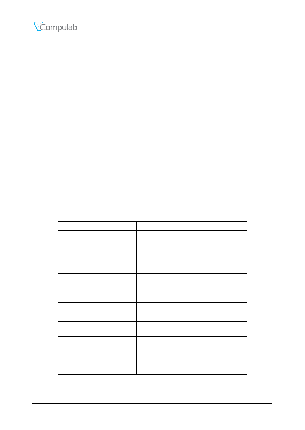
4.1 Display Interface
CM-T43 Display interface is derived from the Sitara AM437x display subsystem (DSS). The DSS
can operate in one of the following modes (depending on software configuration)
RFBI mode (implements MIPI-DBI 2.0 protocol) and supports the following features:
8/9/12/16-bit parallel interface (up to QVGA@30fps)
Two programmable configurations for two devices connected to the RFBI module.
Tearing Effect control logic (Horizontal Synchronization (HSync) and Vertical
Synchronization (VSync) embedded in a single signal (TE) or using two signals
(HS+VS))
Programmable pixel memory formats (12-, 16-, 18- and 24-bit-per-pixel modes in RGB
format)
Programmable output formats on one/multiple cycles per pixel (data from Display
controller and from L4) (TDM)
BYPASS mode (implements MIPI-DPI 1.0 protocol), commonly known as the parallel RGB
interface. The following features are supported in bypass mode:
Programmable pixel rate (up to 100 MHz)
Programmable pixel memory formats (Palletized: 1, 2, 4, 8-bit per pixel; RGB 16, and 24-
bit per pixel and YUV 4:2:2)
Programmable display size (up to 2048 x 2048)
256 x 24-bit entries palette in RGB
For additional details on DSS, please refer to the Sitara AM437x technical reference manual.
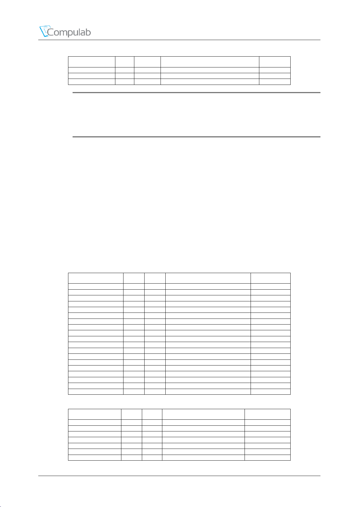
The table below summarizes the display interface signals
Table 5 Display Interface Signals
Revised September 2017 CM-T43 Reference Guide 16
Page 17
Peripheral Interfaces
Signal Name
Pin #
Type
Description
Availability
DSS_DATA17
133*
O
Pixel Data Bus / RFBI Tearing Effect or
Horizontal Sync 0
Without
"N4G"
Without
"N16G"
Without
"N32G"
DSS_DATA18
142*
O
Pixel Data Bus / RFBI Tearing Effect or
Vertical Sync 1
Always
DSS_DATA18
163*
O
Pixel Data Bus / RFBI Tearing Effect or
Vertical Sync 1
Without
"N4G"
Without
"N16G"
Without
"N32G"
DSS_DATA19
144*
O
Pixel Data Bus / RFBI Tearing Effect or
Horizontal Sync 1
Always
DSS_DATA19
161*
O
Pixel Data Bus / RFBI Tearing Effect or
Horizontal Sync 1
Without
"N4G"
Without
"N16G"
Without
"N32G"
DSS_DATA2
110*^
IO; PD
Pixel Data Bus / RFBI Data
10KΩ Pull Down onboard CM-T43
Always
DSS_DATA20
146*
O
Pixel Data Bus / RFBI Chip Select 0
Always
DSS_DATA20
149*
O
Pixel Data Bus
Without
"N4G"
Without
"N16G"
Without
"N32G"
DSS_DATA21
148*
O
Pixel Data Bus
Always
DSS_DATA21
151*
O
Pixel Data Bus
Without
"N4G"
Without
"N16G"
Without
"N32G"
DSS_DATA22
74* O Pixel Data Bus
Always
DSS_DATA22
153*
O
Pixel Data Bus
Without
"N4G"
Without
"N16G"
Without
"N32G"
DSS_DATA23
76* O Pixel Data Bus
Always
DSS_DATA23
155*
O
Pixel Data Bus
Without
"N4G"
Without
"N16G"
Without
"N32G"
DSS_DATA3
112*^
IO;
PU33/PD
Pixel Data Bus / RFBI Data; Pulled high/low
on
SoM when normal/alternate boot sequence is
selected respectively
Always
DSS_DATA4
116*^
IO;
PD/PU33
Pixel Data Bus / RFBI Data; Pulled low/high
on SoM when normal/alternate boot sequence
is selected respectively
Always
DSS_DATA5
118*^
IO; PD
Pixel Data Bus / RFBI Data
10KΩ Pull Down onboard CM-T43
Always
DSS_DATA6
120*^
IO; PD
Pixel Data Bus / RFBI Data
10KΩ Pull Down onboard CM-T43
Always
DSS_DATA7
122*^
IO; PD
Pixel Data Bus / RFBI Data
10KΩ Pull Down onboard CM-T43
Always
DSS_DATA8
124*^
IO; PD
Pixel Data Bus / RFBI Data
10KΩ Pull Down onboard CM-T43
Always
DSS_DATA9
126*^
IO; PD
Pixel Data Bus / RFBI Data
10KΩ Pull Down onboard CM-T43
Always
DSS_HSYNC
100*^
O; PD
Horizontal Sync / RFBI Chip Select 0
Always
Revised September 2017 CM-T43 Reference Guide 17
Page 18
Peripheral Interfaces
Signal Name
Pin #
Type
Description
Availability
10KΩ Pull Down onboard CM-T43
DSS_PCLK
98* O Pixel Clock / RFBI Read 1 Enable
Always
DSS_VSYNC
102*^
O; PD
Always
Signal Name
Pin #
Type
Description
Availability
CAM0_DATA0
109*
I
Camera/VPFE data
Always
CAM0_DATA1
107*
I
Camera/VPFE data
Always
CAM0_DATA10
99*
I
Camera/VPFE data
Always
CAM0_DATA10
148*
I
Camera/VPFE data
Always
CAM0_DATA11
127*
I
Camera/VPFE data
Always
CAM0_DATA11
146*
I
Camera/VPFE data
Always
CAM0_DATA2
121*
I
Camera/VPFE data
Always
CAM0_DATA3
119*
I
Camera/VPFE data
Always
CAM0_DATA4
97*
I
Camera/VPFE data
Always
CAM0_DATA5
75*
I
Camera/VPFE data
Always
CAM0_DATA6
73*
I
Camera/VPFE data
Always
CAM0_DATA7
81*
I
Camera/VPFE data
Always
CAM0_DATA8
142*
I
Camera/VPFE data
Always
CAM0_DATA9
92*
I
Camera/VPFE data
Always
CAM0_FIELD
148*
IO
CCD Data Field Indicator
Always
CAM0_HD
76*
IO
CCD Data Horizontal Detect
Always
CAM0_PCLK
144*
I
CCD Data Pixel Clock
Always
CAM0_VD
74*
IO
CCD Data Vertical Detect
Always
CAM0_WEN
146*
I
CCD Data Write Enable
Always
Signal Name
Pin #
Type
Description
Availability
CAM1_DATA0
101*
I
Camera/VPFE data
Always
CAM1_DATA1
103*
I
Camera/VPFE data
Always
CAM1_DATA10
99* I Camera/VPFE data
Always
CAM1_DATA10
121*
I
Camera/VPFE data
Always
CAM1_DATA10
148*
I
Camera/VPFE data
Always
CAM1_DATA11
119*
I
Camera/VPFE data
Always
CAM1_DATA11
127*
I
Camera/VPFE data
Always
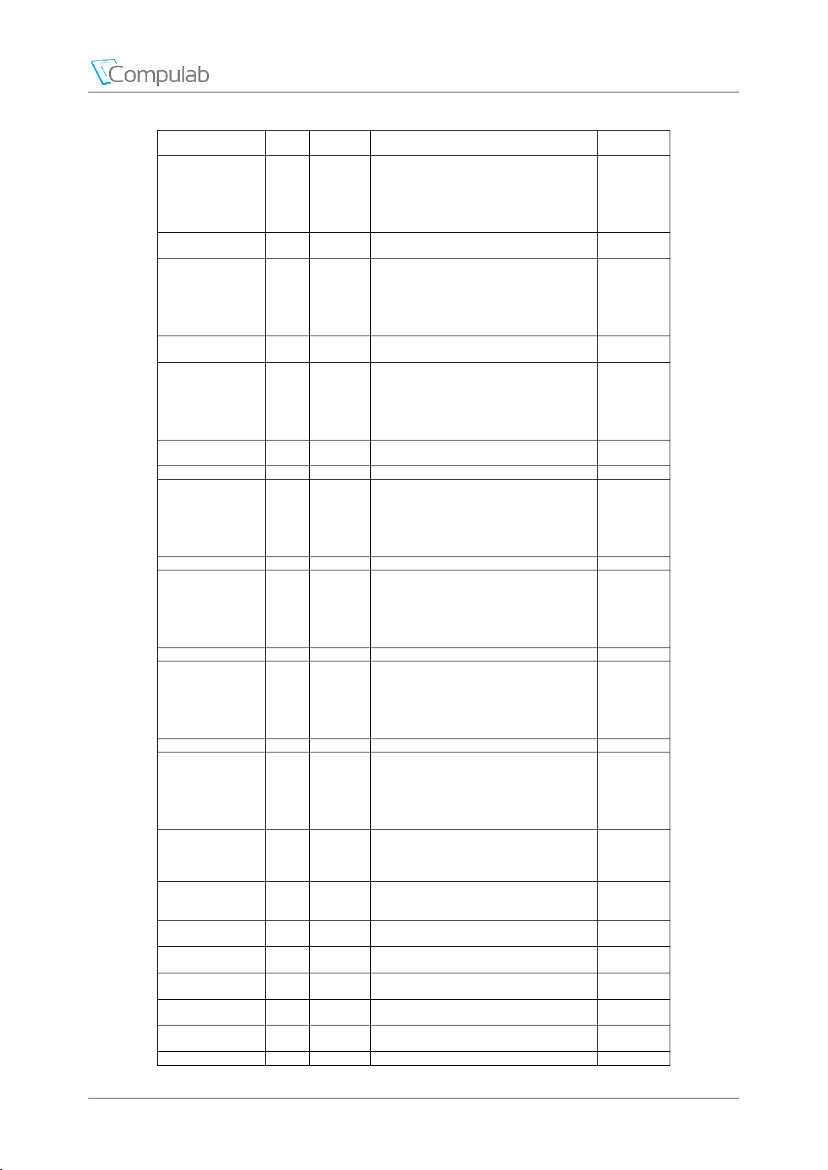
NOTE: Pins denoted with "*" are multifunctional. For additional details please refer to
chapter 5.5 of this document
NOTE: Pins denoted with "^" must not be pulled or driven by carrier board during SoM
power-up / reset.
4.2 Camera Interfaces (VPFE)
CM-T43 camera interfaces are derived from the Sitara AM437x integrated Video Port Front End
(VPFE) modules. CM-T43 includes two instantiations of the VPFE for connection to CCD cameras
or BT.656 compliant video encoders. The following main features are supported:
Dual Port 8- and 10-Bit BT656 Interface
Dual Port 8- and 10-Bit Including External Syncs
Single Port 12-Bit
YUV422/RGB422 and BT656 Input Format
RAW Format
Pixel Clock Rate Up to 75 MHz
For additional details on VPFE, please refer to the Sitara AM437x technical reference manual. The
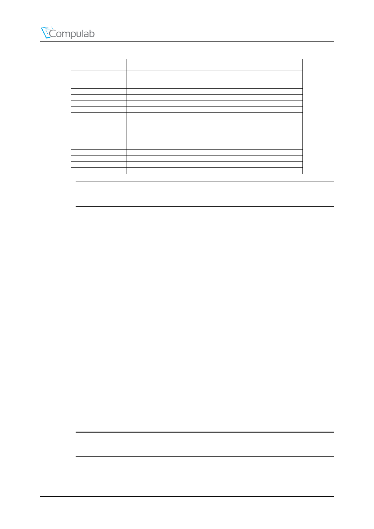
tables below summarize the camera interface signals
Table 6 Camera Port 0 Interface Signals
Table 7 Camera Port 1 Interface Signals
Revised September 2017 CM-T43 Reference Guide 18
Page 19
Peripheral Interfaces
Signal Name
Pin #
Type
Description
Availability
CAM1_DATA11
146*
I
Camera/VPFE data
Always
CAM1_DATA2
89* I Camera/VPFE data
Without "WB"
CAM1_DATA3
91* I Camera/VPFE data
Without "WB"
CAM1_DATA4
77* I Camera/VPFE data
Without "WB"
CAM1_DATA5
79* I Camera/VPFE data
Without "WB"
CAM1_DATA6
83* I Camera/VPFE data
Without "WB"
CAM1_DATA7
85* I Camera/VPFE data
Without "WB"
CAM1_DATA8
93* I Camera/VPFE data
Always
CAM1_DATA8
107*
I
Camera/VPFE data
Always
CAM1_DATA9
94* I Camera/VPFE data
Always
CAM1_DATA9
109*
I
Camera/VPFE data
Always
CAM1_FIELD
99*
IO
CCD Data Field Indicator
Always
CAM1_HD
115*
IO
CCD Data Horizontal Detect
Always
CAM1_PCLK
95* I CCD Data Pixel Clock
Always
CAM1_VD
113*
IO
CCD Data Vertical Detect
Always
CAM1_WEN
97* I CCD Data Write Enable
Always
CAM1_WEN
127*
I
CCD Data Write Enable
Always
NOTE: Pins denoted with "*" are multifunctional. For additional details please refer to
chapter 5.5 of this document
4.3 Local Bus (GPMC)
The Local bus interface available with CM-T43 is derived from the general-purpose memory
controller (GPMC) IP built into the Sitara AM437x SoC. The GPMC is a unified memory controller
dedicated to interfacing external memory devices such as SRAM-Like memories, NAND, NOR and
Pseudo-SRAM devices. The following main features are supported with by the GPMC:
Data path to external memory device can be 16- or 8-bit wide
32-bit OCPIP 2.0 compliant core, single slave interface. Support non-wrapping and wrapping
burst up to 16x32bits.
Up to 100 MHz external memory clock performance (single device)
Address and Data multiplexed access
Support 512M Bytes maximum addressing capability which can be divided into seven
independent chip-select with programmable bank size and base address on 16M Bytes, 32M
Bytes, 64M Bytes, or 128M Bytes boundary
Each chip-select as independent and programmable control signal timing parameters for Setup
and Hold time
Flexible internal access time control (wait state) and flexible handshake mode using external
WAIT pins monitoring (up to two WAIT pins)
Bus keeping and bus turn-around support
Pre-fetch and write posting engine associated with system DMA to get full performance from
NAND device with minimum impact on NOR/SRAM concurrent access
On the fly ECC Hamming Code calculation to improve NAND usage reliability with
minimum impact on SW
Programmable auto-clock gating support
Revised September 2017 CM-T43 Reference Guide 19
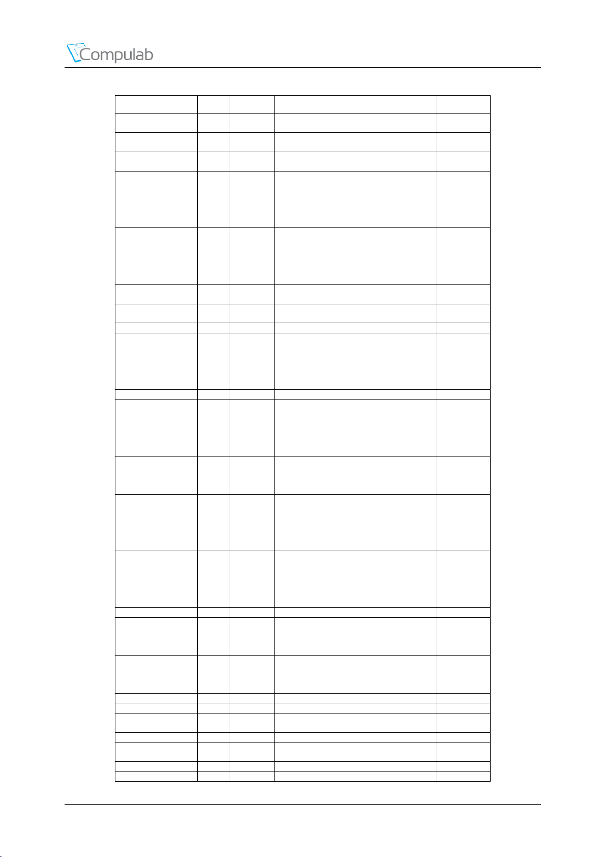
NOTE: Some of the GPMC signals are shared with onboard SLC NAND flash when CM-T43
configuration includes the “N128” or “N512” options.
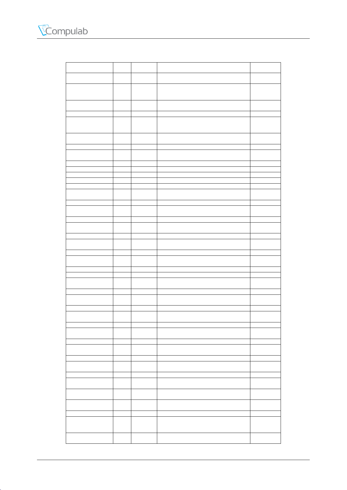
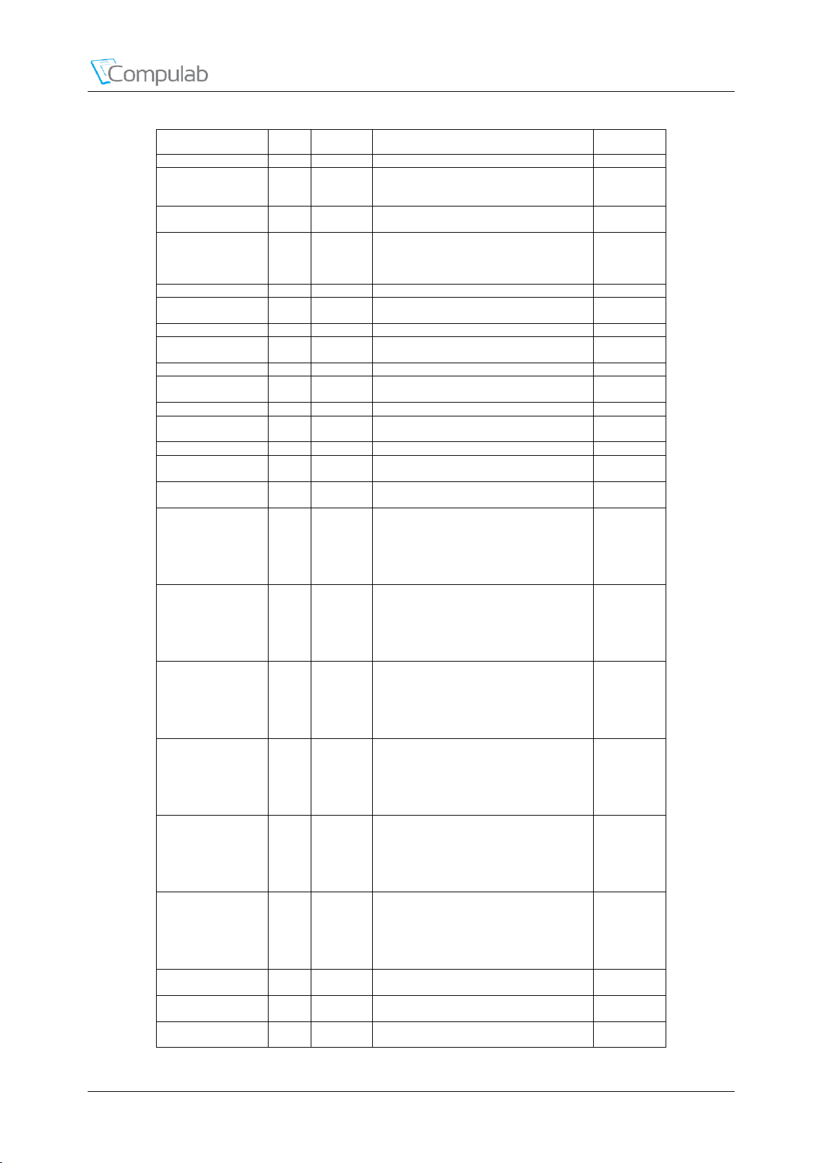
For additional details on GPMC, please refer to the Sitara AM437x technical reference manual. The
table below summarizes the GPMC interface signals
Page 20
Peripheral Interfaces
Signal Name
Pin #
Type
Description
Availability
GPMC_A0
57* O GPMC Address
Without
"E2"
GPMC_A0
106*^
IO;
PU33/PD
GPMC Address; Pulled high/low on SoM
when normal/alternate boot sequence is
selected respectively
Always
GPMC_A1
44* O GPMC Address
Without
"E2"
GPMC_A1
102*^
O; PD
GPMC Address
Always
GPMC_A1
108*^
O;
PD/PU33
GPMC Address; Pulled low/high on SoM
when normal/alternate boot sequence is
selected respectively
Always
GPMC_A10
50* O GPMC Address
Without
"E2"
GPMC_A10
98* O GPMC Address
Always
GPMC_A11
42* O GPMC Address
Without
"E2"
GPMC_A11
104*^
O; PU33
GPMC Address
Always
GPMC_A12
124*^
O; PD
GPMC Address
Always
GPMC_A13
126*^
O; PD
GPMC Address
Always
GPMC_A14
128*^
O; PD
GPMC Address
Always
GPMC_A15
130*^
O; PD
GPMC Address
Always
GPMC_A16
57* O GPMC Address
Without
"E2"
GPMC_A16
134*^
O; PD
GPMC Address
Always
GPMC_A17
44* O GPMC Address
Without
"E2"
GPMC_A17
136*^
O; PD
GPMC Address
Always
GPMC_A18
36* O GPMC Address
Without
"E2"
GPMC_A18
138*^
O; PD
GPMC Address
Always
GPMC_A19
38* O GPMC Address
Without
"E2"
GPMC_A19
140*^
O; PU33
GPMC Address
Always
GPMC_A2
36* O GPMC Address
Without
"E2"
GPMC_A2
100*^
O; PD
GPMC Address
Always
GPMC_A2
110*^
O; PD
GPMC Address
Always
GPMC_A20
30* O GPMC Address
Without
"E2"
GPMC_A20
90* O GPMC Address
Always
GPMC_A21
32* O GPMC Address
Without
"E2"
GPMC_A21
88* O GPMC Address
Always
GPMC_A22
40* O GPMC Address
Without
"E2"
GPMC_A22
86* O GPMC Address
Always
GPMC_A23
47* O GPMC Address
Without
"E2"
GPMC_A23
84* O GPMC Address
Always
GPMC_A24
34* O GPMC Address
Without
"E2"
GPMC_A24
80* O GPMC Address
Always
GPMC_A25
48* O GPMC Address
Without
"E2"
GPMC_A25
82* O GPMC Address
Always
GPMC_A26
50* O GPMC Address
Without
"E2"
GPMC_A27
42* O GPMC Address
Without
"E2"
GPMC_A3
38* O GPMC Address
Without
"E2"
GPMC_A3
98* O GPMC Address
Always
GPMC_A3
112*^
O;
PU33/PD
GPMC Address; Pulled high/low on SoM
when normal/alternate boot sequence is
selected respectively
Always
GPMC_A4
30* O GPMC Address
Without
"E2"
Table 8 GPMC Interface Signals
Revised September 2017 CM-T43 Reference Guide 20
Page 21
Peripheral Interfaces
Signal Name
Pin #
Type
Description
Availability
GPMC_A4
104*^
O; PU33
GPMC Address
Always
GPMC_A4
116*^
O;
PD/PU33
GPMC Address; Pulled low/high on SoM
when normal/alternate boot sequence is
selected respectively
Always
GPMC_A5
32* O GPMC Address
Without
"E2"
GPMC_A5
41* O GPMC Address
Without
"N128"
Without
"N512"
GPMC_A5
118*^
O; PD
GPMC Address
Always
GPMC_A6
40* O GPMC Address
Without
"E2"
GPMC_A6
120*^
O; PD
GPMC Address
Always
GPMC_A7
47* O GPMC Address
Without
"E2"
GPMC_A7
122*^
O; PD
GPMC Address
Always
GPMC_A8
34* O GPMC Address
Without
"E2"
GPMC_A8
102*^
O; PD
GPMC Address
Always
GPMC_A9
48* O GPMC Address
Without
"E2"
GPMC_A9
100*^
O; PD
GPMC Address
Always
GPMC_AD0
21
IO
GPMC Address and Data
Always
(shared)
GPMC_AD1
23
IO
GPMC Address and Data
Always
(shared)
GPMC_AD10
151*
IO
GPMC Address and Data
Without
"N4G"
Without
"N16G"
Without
"N32G"
GPMC_AD11
149*
IO
GPMC Address and Data
Without
"N4G"
Without
"N16G"
Without
"N32G"
GPMC_AD12
161*
IO
GPMC Address and Data
Without
"N4G"
Without
"N16G"
Without
"N32G"
GPMC_AD13
163*
IO
GPMC Address and Data
Without
"N4G"
Without
"N16G"
Without
"N32G"
GPMC_AD14
133*
IO
GPMC Address and Data
Without
"N4G"
Without
"N16G"
Without
"N32G"
GPMC_AD15
131*
IO
GPMC Address and Data
Without
"N4G"
Without
"N16G"
Without
"N32G"
GPMC_AD2
25
IO
GPMC Address and Data
Always
(shared)
GPMC_AD3
27
IO
GPMC Address and Data
Always
(shared)
GPMC_AD4
29
IO
GPMC Address and Data
Always
(shared)
Revised September 2017 CM-T43 Reference Guide 21
Page 22
Peripheral Interfaces
Signal Name
Pin #
Type
Description
Availability
GPMC_AD5
31
IO
GPMC Address and Data
Always
(shared)
GPMC_AD6
33
IO
GPMC Address and Data
Always
(shared)
GPMC_AD7
35
IO
GPMC Address and Data
Always
(shared)
GPMC_AD8
155*
IO
GPMC Address and Data
Without
"N4G"
Without
"N16G"
Without
"N32G"
GPMC_AD9
153*
IO
GPMC Address and Data
Without
"N4G"
Without
"N16G"
Without
"N32G"
GPMC_ADVN_ALE
45
O
GPMC Address Valid
Address Latch Enable
Always
(shared)
GPMC_BE0N_CLE
41
O
GPMC Byte Enable 0
Command Latch Enable
Always
(shared)
GPMC_BE1N
43* O GPMC Byte Enable 1
Always
GPMC_BE1N
147*
O
GPMC Byte Enable 1
Without
"N4G"
Without
"N16G"
Without
"N32G"
GPMC_CLK
39*
IO
GPMC Clock
Always
GPMC_CLK
157*
IO
GPMC Clock
Without
"N4G"
Without
"N16G"
Without
"N32G"
GPMC_CSN0
162*
O
GPMC Chip Select
Without
"N128"
Without
"N512"
GPMC_CSN1
157*
O
GPMC Chip Select
Without
"N4G"
Without
"N16G"
Without
"N32G"
GPMC_CSN2
147*
O
GPMC Chip Select
Without
"N4G"
Without
"N16G"
Without
"N32G"
GPMC_CSN3
202*
O
GPMC Chip Select
Always
GPMC_CSN4
51* O GPMC Chip Select
Without
"N128"
Without
"N512"
GPMC_CSN5
59* O GPMC Chip Select
Without
"N128"
Without
"N512"
GPMC_CSN6
43* O GPMC Chip Select
Always
GPMC_DIR
43* O GPMC Data Direction
Always
GPMC_OEN_REN
49
O
GPMC Output
Read Enable
Always
(shared)
GPMC_WAIT0
202*
I
GPMC Wait 0
Always
GPMC_WAIT0
51 I GPMC Wait 0
Always
(shared)
GPMC_WAIT1
39* I GPMC Wait 1
Always
GPMC_WEN
53 O GPMC Write Enable
Always
Revised September 2017 CM-T43 Reference Guide 22
Page 23
Peripheral Interfaces
Signal Name
Pin #
Type
Description
Availability
(shared)
GPMC_WPN
59 O GPMC Write Protect
Always
(shared)
Parameter
Test conditions
Min
Typ
Max
Unit
Stereo Headphone Output
0-dB full-scale output voltage
1.0 Vrms
Maximum output power, PO
R
load
= 32Ω
30
mW
R
load
= 16Ω
50
Signal-to-noise ratio, Aweighted
90
97 dB
Total harmonic distortion
1kHz output,
Rload = 32Ω,
P
out
= 10mW
rms (-5dB)
0.056
-65
0.1
60 % dB
P
out
= 20mW
rms (-2dB)
0.56
-45
1.0
40 % dB
Power supply rejection ratio
1 kHz, 100 mV
p-p
50
dB
20Hz – 20kHz, 100mV
p-p
45
Programmable gain
1 kHz output
-73 0 6
dB
Programmable-gain step size
1 kHz
1
dB
Mute attenuation
1 kHz output, 0dB
80 dB
Line Input to ADC
Input signal level (0 dB)
1.0 Vrms
Signal-to-noise ratio
A-weighted, 0dB gain,
Fsample = 48 kHz.
85
90
dB
A-weighted, 0dB gain,
Fsample = 96 kHz.
90 Dynamic range
A-weighted, −60-dB full-scale
input
85
90 dB
Total harmonic distortion
−1-dB input, 0-dB gain
-84
0.006
-74
0.02
dB
%
Power supply rejection ratio
1 kHz, 100 mV
p-p
50
dB
20Hz – 20kHz, 100mV
p-p
45
ADC Channel Separation
1 kHz input tone
90 dB
Programmable-gain
1 kHz input tone,
Rsource<50Ω
-34.5 0 +12
dB
Programmable-gain step size
Guaranteed Monotonic
1.5 dB
Mute attenuation
0dB, 1 kHz input tone
80 dB
Input resistance
12 dB input gain
10
15
kΩ
0 dB input gain
20
30
Input capacitance
10 pF
NOTE: Pins denoted with "*" are multifunctional. For additional details please refer to
chapter 5.5 of this document
NOTE: Pins denoted with "^" must not be pulled or driven by carrier board during SoM
power-up / reset.
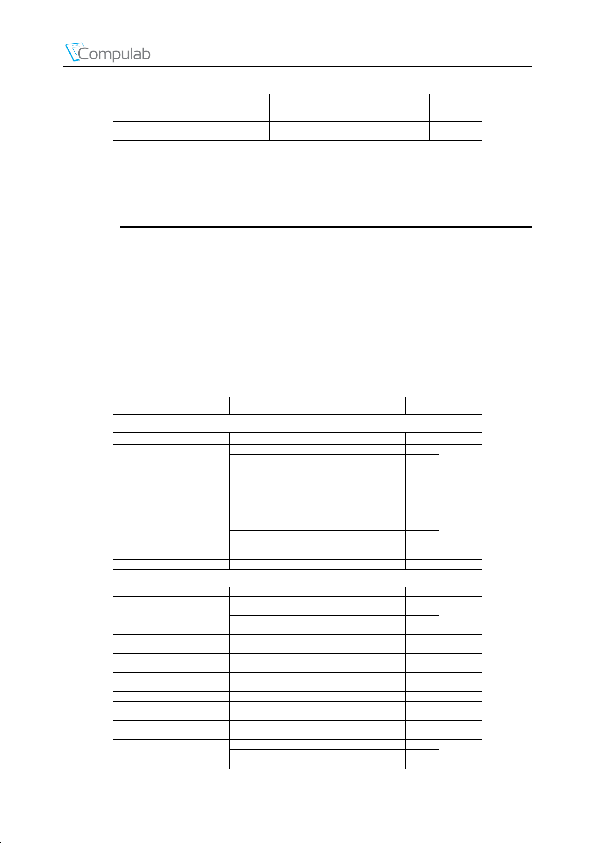
4.4 Analog Audio
The CM-T43 analog audio functionality is implemented by interfacing the Wolfson WM8731L audio
codec with the Sitara AM437x McASP0 interface. The codec supports the following features:
Highly Efficient Headphone driver
Audio performance (‘A’ weighted): ADC SNR – 90dB, DAC SNR – 100dB.
Microphone input and electret bias with side tone mixer
ADC and DAC sampling frequency: 8kHz – 96kHz.
Selectable ADC high pass filter
Table 9 Analog Audio Characteristics
Revised September 2017 CM-T43 Reference Guide 23
Page 24
Peripheral Interfaces
Parameter
Test conditions
Min
Typ
Max
Unit
Microphone Input to ADC
Input signal level (0 dB)
1.0 Vrms
Signal-to-noise ratio
A-weighted, 0-dB gain
85 dB
Dynamic range,
A-weighted, −60-dB full-scale
input
85 dB
Total harmonic distortion,
0dB input, 0dB gain
-60
-55
dB
Power supply rejection ratio
1 kHz, 100 mV
p-p
50
dB
20Hz – 20kHz, 100mV
p-p
45
Programmable-gain Boost
1kHz input, Rsource<50Ω,
MICBOOST bit is 1.
34 dB
Mic Path gain (MICBOOST
gain is additional to this
nominal gain)
MICBOOST bit is 0,
Rsource<50Ω,
14 dB
Mute attenuation
0dB, 1 kHz input tone
80 dB
Input resistance
10 kΩ
Input capacitance
10 pF
Microphone Bias
Bias voltage
2.375
2.475
2.575
V
Bias-current source
3 mA
Output noise voltage
1kHz to 20kHz
25 nV/√Hz
Signal Name
Pin #
Type
Description
Availability
LLINEIN
199
AI
Left channel line input
With "A"
LLINEOUT
203
AO
Left channel headphone output
With "A"
MICBIAS
191
APO
Electret microphone bias supply
With "A"
MICIN
193
AI
Microphone input
With "A"
RLINEIN
197
AI
Right channel line input
With "A"
RLINEOUT
201
AO
Right channel headphone output
With "A"
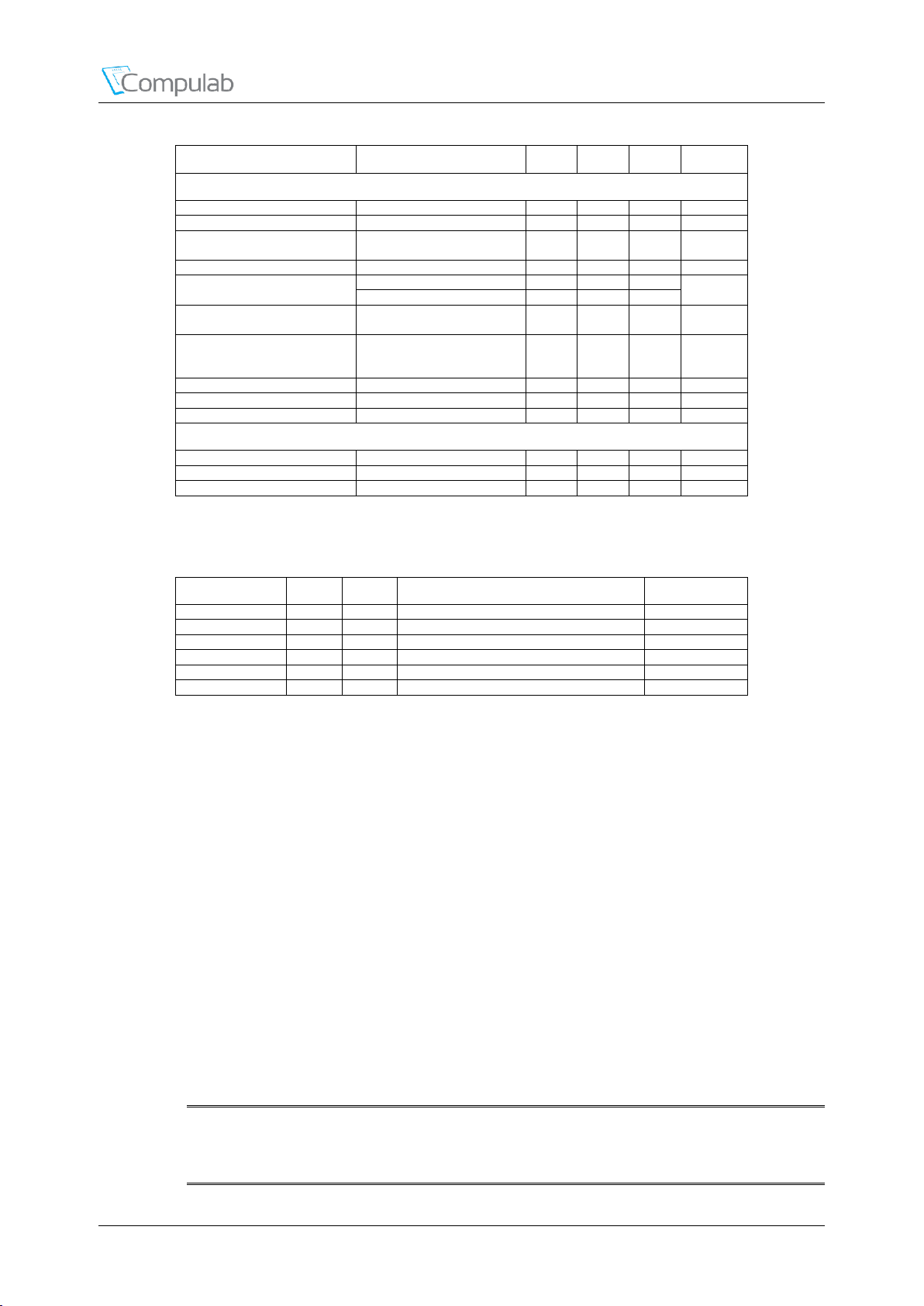
For additional details on the codec, please refer to the Wolfson WM8731L datasheet. The table below
summarizes the analog audio interface signals
Table 10 Analog Audio Interface Signals
4.5 Digital Audio (McASP)
The multichannel digital audio interface available with CM-T43 is based on the multichannel audio
serial port IP integrated into Sitara AM437x SoC. Two instances of the McASP block are available
with CM-T43. McASP supports the following main features:
S/PDIF, IEC60958-1, AES-3 formats (DIT)
Wide variety of I2S and similar bit-stream formats
S/PDIF, IEC60958-1, AES-3 formats – Transmit section only
TDM stream of 384 time slots specifically designed for easy interface to external digital
interface receiver (DIR) device transmitting DIR frames to McASP using the I2S protocol
(one time slot for each DIR subframe) – Receive section only
Programmable clock and frame sync polarity (rising or falling edge): ACLKR/X, HCLKR/X,
and AFSR/X
Slot length (number of bits per time slot): 8, 12, 16, 20, 24, 28, 32 bits supported
Word length (bits per word): 8, 12, 16, 20, 24, 28, 32 bits; always less than or equal to the ime
slot length
Revised September 2017 CM-T43 Reference Guide 24
For additional details on McASP, please refer to the Sitara AM437x technical reference manual.
NOTE: Usage of the McASP0 interface signals on the carrier board when CM-T43
configuration includes the “A” option, will render the onboard analog audio codec
inoperable.
Page 25
Peripheral Interfaces
Signal Name
Pin #
Type
Description
Availability
MCASP0_ACLKR
26*
IO
McASP0 Receive Bit Clock
Without "E1"
MCASP0_ACLKR
43*
IO
McASP0 Receive Bit Clock
Always
MCASP0_ACLKR
134*^
IO; PD
McASP0 Receive Bit Clock
Always
MCASP0_ACLKR
198*
IO
McASP0 Receive Bit Clock
Always
MCASP0_ACLKX
8*
IO
McASP0 Transmit Bit Clock
Without "E1"
MCASP0_ACLKX
34*
IO
McASP0 Transmit Bit Clock
Without "E2"
MCASP0_ACLKX
124*^
IO; PD
McASP0 Transmit Bit Clock
Always
MCASP0_ACLKX
161*
IO
McASP0 Transmit Bit Clock
Without "N4G"
Without "N16G"
Without "N32G"
MCASP0_ACLKX
199*
IO
McASP0 Transmit Bit Clock
Without "A"
MCASP0_AHCLKR
125*
IO
McASP0 Receive Master Clock
Always
MCASP0_AHCLKR
130*^
IO; PD
McASP0 Receive Master Clock
Always
MCASP0_AHCLKX
62*
IO
McASP0 Transmit Master Clock
Without "E1"
MCASP0_AHCLKX
140*^
IO; PU33
McASP0 Transmit Master Clock
Always
MCASP0_AHCLKX
193*
IO
McASP0 Transmit Master Clock
Without "A"
MCASP0_AXR0
20*
IO
McASP0 Serial Data (IN/OUT)
Without "E1"
MCASP0_AXR0
50*
IO
McASP0 Serial Data (IN/OUT)
Without "E2"
MCASP0_AXR0
128*^
IO; PD
McASP0 Serial Data (IN/OUT)
Always
MCASP0_AXR0
133*
IO
McASP0 Serial Data (IN/OUT)
Without "N4G"
Without "N16G"
Without "N32G"
MCASP0_AXR0
197*
IO
McASP0 Serial Data (IN/OUT)
Without "A"
MCASP0_AXR1
18*
IO
McASP0 Serial Data (IN/OUT)
Without "E1"
MCASP0_AXR1
42*
IO
McASP0 Serial Data (IN/OUT)
Without "E2"
MCASP0_AXR1
131*
IO
McASP0 Serial Data (IN/OUT)
Without "N4G"
Without "N16G"
Without "N32G"
MCASP0_AXR1
138*^
IO; PD
McASP0 Serial Data (IN/OUT)
Always
MCASP0_AXR1
203*
IO
McASP0 Serial Data (IN/OUT)
Without "A"
MCASP0_AXR2
125*
IO
McASP0 Serial Data (IN/OUT)
Always
MCASP0_AXR2
130*^
IO; PD
McASP0 Serial Data (IN/OUT)
Always
MCASP0_AXR2
134*^
IO; PD
McASP0 Serial Data (IN/OUT)
Always
MCASP0_AXR2
143*
IO
McASP0 Serial Data (IN/OUT)
Without "WB"
MCASP0_AXR2
198*
IO
McASP0 Serial Data (IN/OUT)
Always
MCASP0_AXR3
22*
IO
McASP0 Serial Data (IN/OUT)
Without "E1"
MCASP0_AXR3
111*
IO
McASP0 Serial Data (IN/OUT)
Always
MCASP0_AXR3
136*^
IO; PD
McASP0 Serial Data (IN/OUT)
Always
MCASP0_AXR3
140*^
IO; PU33
McASP0 Serial Data (IN/OUT)
Always
MCASP0_AXR3
193*
IO
McASP0 Serial Data (IN/OUT)
Without "A"
MCASP0_FSR
14*
IO
McASP0 Receive Frame Sync
Without "E1"
MCASP0_FSR
39*
IO
McASP0 Receive Frame Sync
Always
MCASP0_FSR
111*
IO
McASP0 Receive Frame Sync
Always
MCASP0_FSR
136*^
IO; PD
McASP0 Receive Frame Sync
Always
MCASP0_FSX
24*
IO
McASP0 Transmit Frame Sync
Without "E1"
MCASP0_FSX
48*
IO
McASP0 Transmit Frame Sync
Without "E2"
MCASP0_FSX
126*^
IO; PD
McASP0 Transmit Frame Sync
Always
MCASP0_FSX
163*
IO
McASP0 Transmit Frame Sync
Without "N4G"
Without "N16G"
Without "N32G"
MCASP0_FSX
201*
IO
McASP0 Transmit Frame Sync
Without "A"
Signal Name
Pin #
Type
Description
Availability
MCASP1_ACLKR
16*
IO
McASP1 Receive Bit Clock
Without "E1"
MCASP1_ACLKR
22*
IO
McASP1 Receive Bit Clock
Without "E1"
MCASP1_ACLKX
26*
IO
McASP1 Transmit Bit Clock
Without "E1"
MCASP1_ACLKX
137*
IO
McASP1 Transmit Bit Clock
Without "WB"
MCASP1_ACLKX
198*
IO
McASP1 Transmit Bit Clock
Always
MCASP1_AHCLKR
22*
IO
McASP1 Receive Master Clock
Without "E1"
MCASP1_AHCLKX
22*
IO
McASP1 Transmit Master Clock
Without "E1"
MCASP1_AHCLKX
139*
IO
McASP1 Transmit Master Clock
Without "WB"
MCASP1_AXR0
6*
IO
McASP1 Serial Data (IN/OUT)
Without "E1"
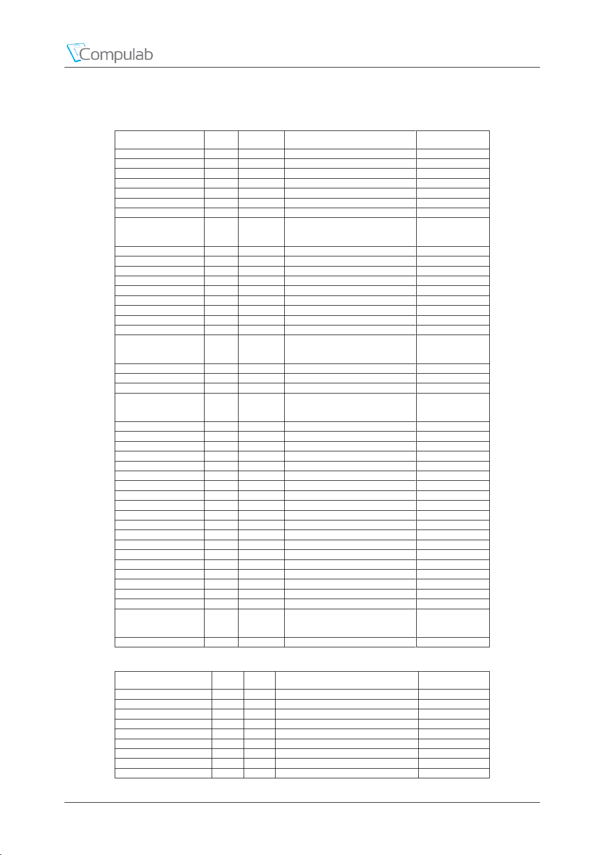
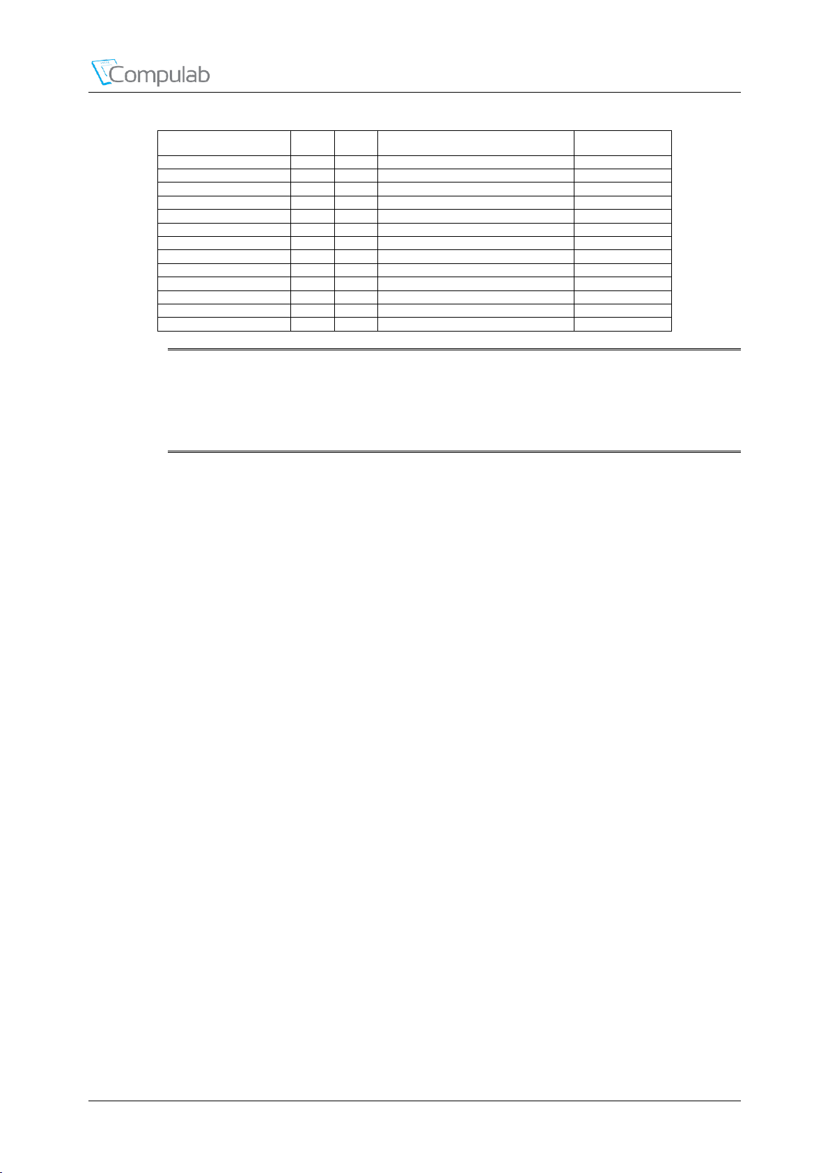
The tables below summarize the McASP interface signals
Table 11 McASP0 Interface Signals
Revised September 2017 CM-T43 Reference Guide 25
Table 12 McASP1 Interface Signals
Page 26
Peripheral Interfaces
Signal Name
Pin #
Type
Description
Availability
MCASP1_AXR0
62*
IO
McASP1 Serial Data (IN/OUT)
Without "E1"
MCASP1_AXR0
203*
IO
McASP1 Serial Data (IN/OUT)
Without "A"
MCASP1_AXR1
12*
IO
McASP1 Serial Data (IN/OUT)
Without "E1"
MCASP1_AXR1
193*
IO
McASP1 Serial Data (IN/OUT)
Without "A"
MCASP1_AXR2
16*
IO
McASP1 Serial Data (IN/OUT)
Without "E1"
MCASP1_AXR2
143*
IO
McASP1 Serial Data (IN/OUT)
Without "WB"
MCASP1_AXR3
4*
IO
McASP1 Serial Data (IN/OUT)
Without "E1"
MCASP1_AXR3
139*
IO
McASP1 Serial Data (IN/OUT)
Without "WB"
MCASP1_FSR
4*
IO
McASP1 Receive Frame Sync
Without "E1"
MCASP1_FSR
12*
IO
McASP1 Receive Frame Sync
Without "E1"
MCASP1_FSX
14*
IO
McASP1 Transmit Frame Sync
Without "E1"
MCASP1_FSX
111*
IO
McASP1 Transmit Frame Sync
Always
MCASP1_FSX
145*
IO
McASP1 Transmit Frame Sync
Without "WB"
NOTE: Pins denoted with "*" are multifunctional. For additional details please refer to
chapter 5.5 of this document
NOTE: Pins denoted with "^" must not be pulled or driven by carrier board during SoM
power-up / reset.
4.6 WLAN, Bluetooth and NFC
CM-T43 features IEEE 802.11ac/a/b/g/n 2X2 MIMO WLAN, Bluetooth & NFC. The functionality is
implemented by interfacing the AzureWave AW-CH397 combo controller module with the Sitara
AM437x MMC/SD/SDIO 2 interface. Based on Marvell 88W8897 chipset, the AW-CH397 supports
the following features:
WLAN IEEE 802.11a/b/g/n/ac, Data Rates:
802.11b: 1, 2, 5.5, 11Mbps
802.11a/g: 6, 9, 12, 18, 24, 36, 48, 54Mbps
802.11n: up to 150Mbps-single
802.11n: up to 300Mbps-2x2 MIMO
802.11ac:up to 192.6Mbps (20MHz channel)
802.11ac:up to 400Mbps (40MHz channel)
802.11ac:up to 866.7Mbps (80MHz channel)
Security features:
WAPI
WEP 64-bit and 128-bit encryption with H/W TKIP processing
WPA/WPA2 (Wi-Fi Protected Access)
AES-CCMP hardware implementation as part of 802.11i security standard
Bluetooth Features:
Bluetooth 4.0 complaint with Bluetooth 2.1+Enhanced Data Rate (EDR) of 1,2, and 3Mbps
NFC Features:
Revised September 2017 CM-T43 Reference Guide 26
Full protocol support for ISO 14443A/B, ISO 18092, ISO 15693, NFCIP-1, NFC Forum,
EMV contactless targets with data rates up to 848 Kbps
Co-Existence:
Bluetooth and cell phone(GSM/DCS/WCDMA/UMTS/3G) co-existence
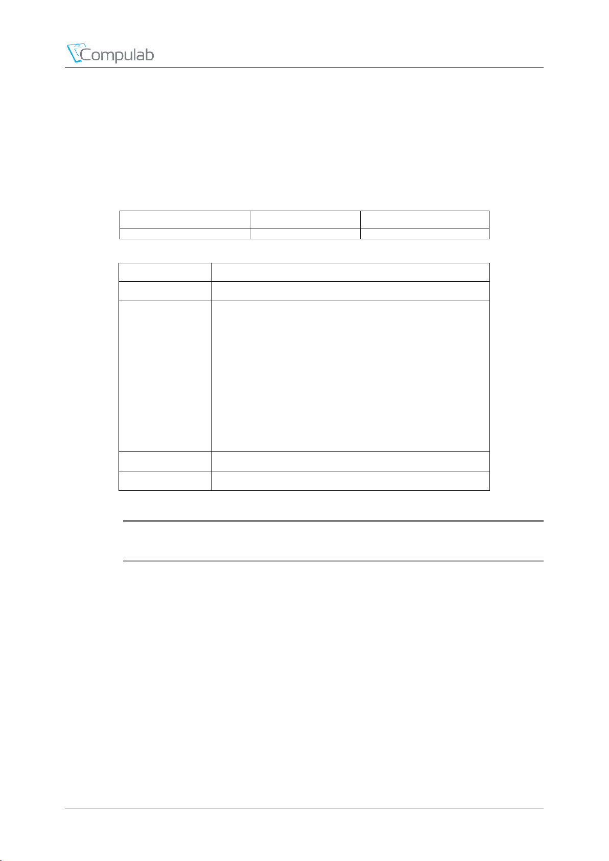
CM-T43 is equipped with three U.FL high frequency connectors:
Page 27
Peripheral Interfaces
Manufacturer
Mfg. P/N
Mating Connector
Hirose
U.FL-R-MT(10)
Hirose U.FL-LP-040
Feature
Description
Frequency Band
2.4 GHz ISM radio band / 5 GHz Unlicensed National Information
Infrastructure (U-NII) band
Number of Channels
802.11a:
USA, Taiwan – 12/4
Most European Countries –19
Japan – 4
802.11b:
USA, Canada and Taiwan – 11
Most European Countries – 13
France – 4
802.11g:
USA, Canada and Taiwan – 11
Most European Countries – 13
Japan – 13
802.11n(HT20):
Channel 1~13(2412~2472)
802.11n(HT40):
Channel 1~7(2422~2472)
Modulation
DSSS, OFDM, DBPSK, DQPSK, CCK, 16-QAM, 64-QAM for WLAN
GFSK (1Mbps), Π/4 DQPSK (2Mbps) and 8DPSK (3Mbps) for Bluetooth
Medium Access
Protocol
CSMA/CA with ACK
Primary WLAN/BT antenna connector J1. Can be used with any type of 2.4GHz/5.0GHz
antenna for WLAN & Bluetooth functionality.
Secondary WLAN antenna connector J2. Can be used with any type of 2.4GHz/5.0GHz
antenna for WLAN MIMO functionality.
NFC antenna connector J3, required for NFC functionality.
Please refer to section 6.3 for locations of J1, J2 and J3.
Table 13 U.FL connector data
Table 14 WLAN RF system specifications
For additional details, please refer to the AzureWave AW-CH397 and Marvell 88W8897 datasheets.
NOTE: The WLAN, Bluetooth and NFC module is available only with the ‘WB’ configuration
option.
4.7 Ethernet
CM-T43 incorporates two full-featured 10/100/1000 ethernet ports implemented with the Sitara
AM437x integrated MAC and the built in 3-port switch coupled with two AR8033 RGMII Ethernet
PHYs from Atheros. Both ethernet interfaces support the following main features:
10/100/1000 BASE-T IEEE 802.3 compliant
IEEE 802.3u compliant Auto-Negotiation
Support for IEEE 1588v2 Clock Synchronization (2008 Annex D, E, and F) - inside the
MAC.
Revised September 2017 CM-T43 Reference Guide 27
Wire rate switching (802.1d)
Page 28
Peripheral Interfaces
Signal Name
Pin
#
Type
Description
Availability
ETH1_LED1
16^
IO;
PD
Active High , 1Gbps link LED driver. 2.5V signal must not
be driven during CM-T43 start-up
With "E1"
ETH1_LED2
4^
IO;
PD
Active High , activity LED driver. 2.5V signal must not be
driven during CM-T43 start-up
With "E1"
ETH1_LED3
22
IO
Active High , 10/100 link LED driver. 2.5V signal must not
be driven during CM-T43 start-up
With "E1"
ETH1_MDI0N
6
AIO
Negative part of 100ohm diff-pair 0
With "E1"
ETH1_MDI0P
8
AIO
Positive part of 100ohm diff-pair 0
With "E1"
ETH1_MDI1N
12
AIO
Negative part of 100ohm diff-pair 1
With "E1"
ETH1_MDI1P
14
AIO
Positive part of 100ohm diff-pair 1
With "E1"
ETH1_MDI2N
18
AIO
Negative part of 100ohm diff-pair 2
With "E1"
ETH1_MDI2P
20
AIO
Positive part of 100ohm diff-pair 2
With "E1"
ETH1_MDI3N
24
AIO
Negative part of 100ohm diff-pair 3
With "E1"
ETH1_MDI3P
26
AIO
Positive part of 100ohm diff-pair 3
With "E1"
Signal Name
Pin
#
Type
Description
Availability
ETH2_LED1
40^
IO;
PD
Active High , 1Gbps link LED driver. 2.5V signal must not
be driven during CM-T43 start-up
With "E2"
ETH2_LED2
57^
IO;
PD
Active High , activity LED driver. 2.5V signal must not be
driven during CM-T43 start-up
With "E2"
ETH2_LED3
34
IO
Active High , 10/100 link LED driver. 2.5V signal must not
be driven during CM-T43 start-up
With "E2"
ETH2_MDI0N
30
AIO
Negative part of 100ohm diff-pair 0
With "E2"
ETH2_MDI0P
32
AIO
Positive part of 100ohm diff-pair 0
With "E2"
ETH2_MDI1N
36
AIO
Negative part of 100ohm diff-pair 1
With "E2"
ETH2_MDI1P
38
AIO
Positive part of 100ohm diff-pair 1
With "E2"
ETH2_MDI2N
42
AIO
Negative part of 100ohm diff-pair 2
With "E2"
ETH2_MDI2P
44
AIO
Positive part of 100ohm diff-pair 2
With "E2"
ETH2_MDI3N
48
AIO
Negative part of 100ohm diff-pair 3
With "E2"
ETH2_MDI3P
50
AIO
Positive part of 100ohm diff-pair 3
With "E2"
Automatic channel swap (ACS)
Full- and Half-duplex
Automatic MDI/MDIX crossover
Automatic polarity correction
Activity and speed indicator LED controls
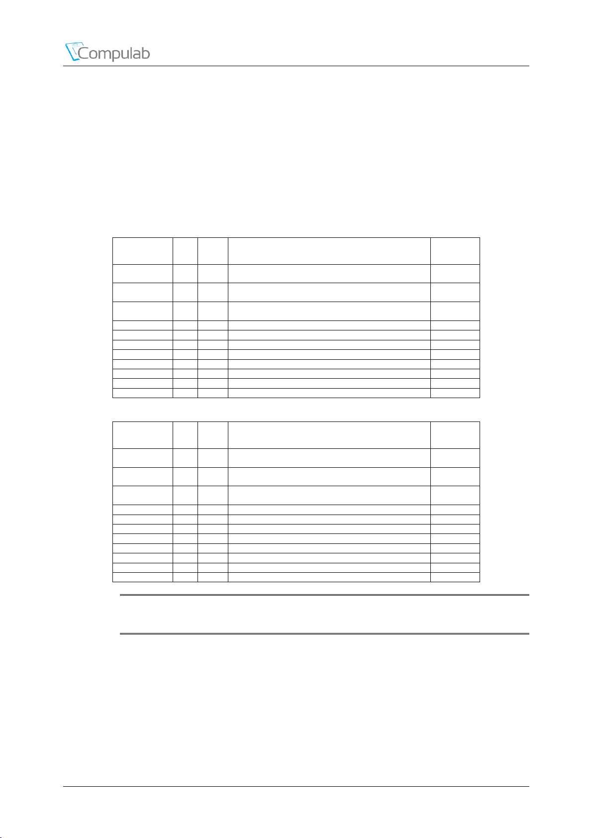
For additional details on the ethernet subsystem, please refer to the Sitara AM437x technical
reference manual. For magnetics selection recommendations, please refer to section 8.3 of this
document. The tables below summarize the ethernet interface signals
Table 15 Ethernet Port 1 Interface Signals
Table 16 Ethernet Port 2 Interface Signals
NOTE: Pins denoted with "^" must not be pulled or driven by carrier board during SoM
power-up / reset.
4.8 USB2.0
CM-T43 is equipped with two independent USB2.0 compliant ports, implemented with two instances
of the Synopsys DWC3 subsystem integrated in the Sitara AM437x SoC. The following main
features are supported:
Both Ports:
Revised September 2017 CM-T43 Reference Guide 28
Page 29
Peripheral Interfaces
Signal Name
Pin #
Type
Description
Availability
USB0_CE
192
AO
USB0 Active high Charger Enable output A
Always
USB0_DM
178
AIO
USB0 Data minus
Always
USB0_DP
176
AIO
USB0 Data plus
Always
USB0_DRVVBUS
200 O USB0 Active high VBUS control output
Always
USB0_ID
174
AIO
USB0 ID
Always
USB0_VBUS
180
API
USB0 VBUS
Always
Signal Name
Pin #
Type
Description
Availability
USB1_DM
170
AIO
USB1 Data minus
Always
USB1_DP
172
AIO
USB1 Data plus
Always
USB1_DRVVBUS
156 O USB1 Active high VBUS control output
Always
USB1_VBUS
196
API
USB1 VBUS
Always
USB 2.0 Host mode at High-Speed (HS, 480 Mbps), Full-Speed (FS, 12 Mbps), and Low-
Speed (LS, 1.5 Mbps)
15 IN (Receive), 15 OUT (Transmit) endpoints (EPs), and one EP0 bidirectional endpoint
All modes of transfers - Control, Bulk, Interrupt, and Isochronous
USB Port0 only:
Dual-Role-Device. Host or Device functionality supported
Supports USB 2.0 Device mode at High-Speed (HS, 480 Mbps), and Full-Speed (FS, 12
Mbps). Low-Speed is not supported in device mode
USB charger detection support. CM-T43 can detect battery chargers connected to USB
Port 0.
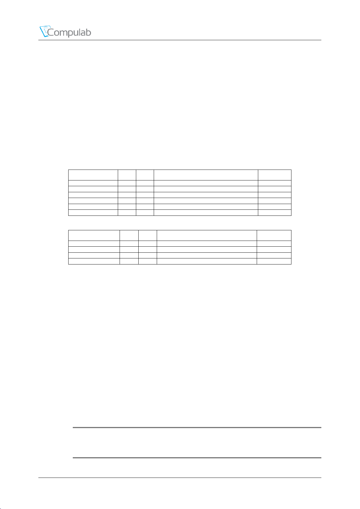
For additional details on the USB subsystem, please refer to the Sitara AM437x technical reference
manual. The tables below summarize the USB interface signals
Table 17 USB Port 0 Interface Signals
Table 18 USB Port 1 Interface Signals
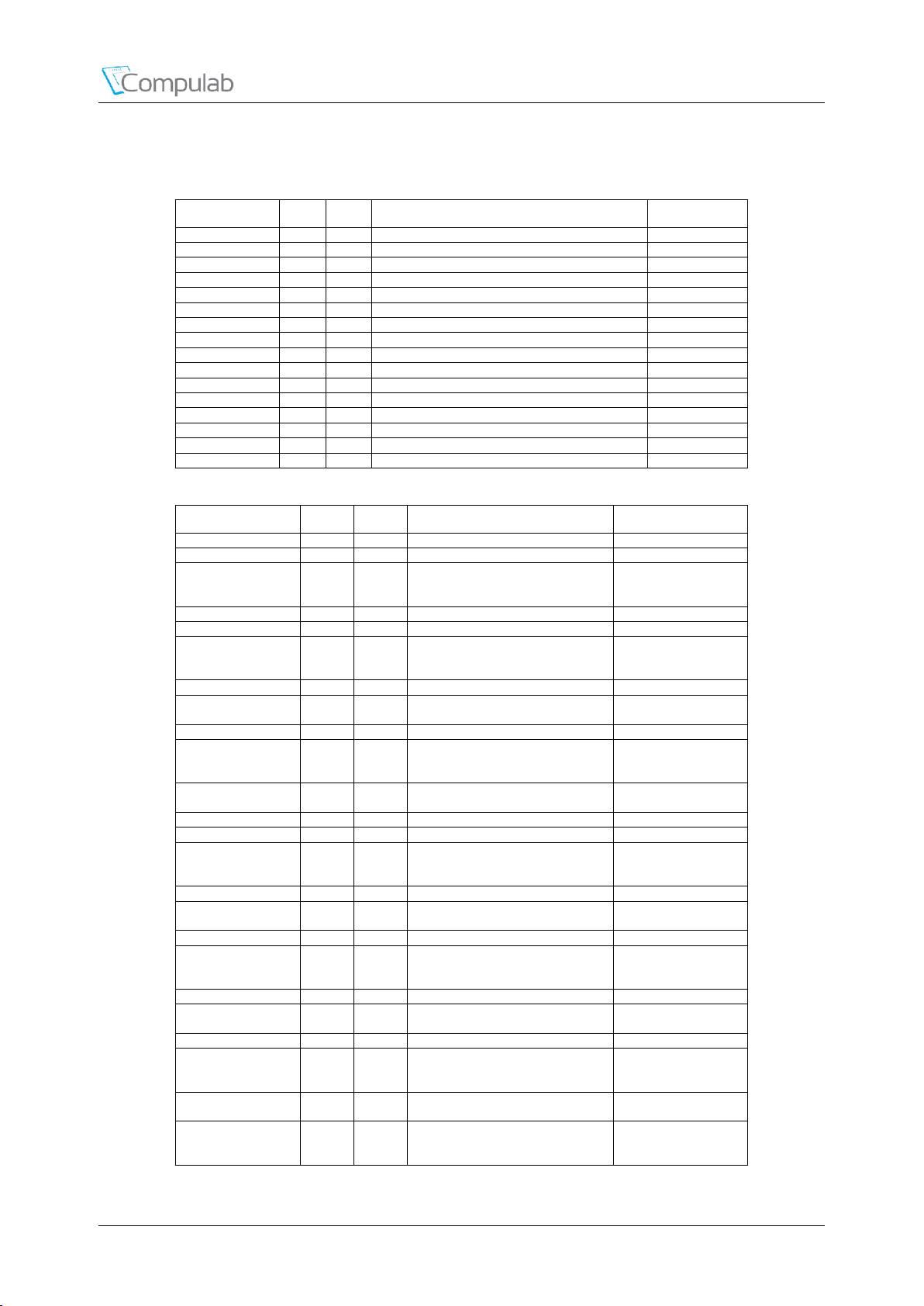
4.9 MMC / SD / SDIO
Up to three full featured MMC/SD/SDIO ports are available with CM-T43. The ports are
implemented with three instances of the MMCSD host controller integrated into the Sitara AM437x
SoC. The following general features are supported:
Up to 384Mbit/sec (48MByte/sec) in MMC mode 8-bit data transfer
Up to 192Mbit/sec (24MByte/sec) in High-Speed SD mode 4-bit data transfer
Up to 24Mbit/sec (3MByte/sec) in Default SD mode 1-bit data transfer
MMC command/response sets as defined in the MMC standard specification v4.3
SD command/response sets as defined in the SD Physical Layer specification v2.00
SDIO command/response sets and interrupt/read-wait suspend-resume operations as defined
in the SD part E1 specification v 2.00
SD Host Controller Standard Specification sets as defined in the SD card specification Part
A2 v2.00
Built-in 1024-byte buffer for read or write
For additional details on the MMC subsystem, please refer to the Sitara AM437x technical reference
manual.
NOTE: Usage of the MMC/SD/SDIO 1 interface signals on the carrier board when CM-T43
Revised September 2017 CM-T43 Reference Guide 29
configuration includes the “N4G”, “N16G” or “N32G” options, will render the
onboard secondary storage device (eMMC) inoperable.
Page 30
Peripheral Interfaces
Signal Name
Pin #
Type
Description
Availability
MMC0_CLK
80*
IO
MMC/SD/SDIO Clock
Always
MMC0_CMD
82*
IO
MMC/SD/SDIO Command
Always
MMC0_DAT0
84*
IO
MMC/SD/SDIO Data Bus
Always
MMC0_DAT1
86*
IO
MMC/SD/SDIO Data Bus
Always
MMC0_DAT2
88*
IO
MMC/SD/SDIO Data Bus
Always
MMC0_DAT3
90*
IO
MMC/SD/SDIO Data Bus
Always
MMC0_DAT4
18*
IO
MMC/SD/SDIO Data Bus
Without "E1"
MMC0_DAT5
20*
IO
MMC/SD/SDIO Data Bus
Without "E1"
MMC0_DAT6
24*
IO
MMC/SD/SDIO Data Bus
Without "E1"
MMC0_DAT7
8*
IO
MMC/SD/SDIO Data Bus
Without "E1"
MMC0_POW
61* O MMC/SD Power Switch Control, Active High
Always
MMC0_POW
139* O MMC/SD Power Switch Control, Active High
Without "WB"
MMC0_SDCD
61* I SD Card Detect
Always
MMC0_SDCD
199* I SD Card Detect
Without "A"
MMC0_SDWP
67* I SD Write Protect
Always
MMC0_SDWP
198* I SD Write Protect
Always
Signal Name
Pin #
Type
Description
Availability
MMC1_CLK
16*
IO
MMC/SD/SDIO Clock
Without "E1"
MMC1_CLK
121*
IO
MMC/SD/SDIO Clock
Always
MMC1_CLK
157*
IO
MMC/SD/SDIO Clock
Without "N4G"
Without "N16G"
Without "N32G"
MMC1_CMD
12*
IO
MMC/SD/SDIO Command
Without "E1"
MMC1_CMD
119*
IO
MMC/SD/SDIO Command
Always
MMC1_CMD
147*
IO
MMC/SD/SDIO Command
Without "N4G"
Without "N16G"
Without "N32G"
MMC1_DAT0
8*
IO
MMC/SD/SDIO Data Bus
Without "E1"
MMC1_DAT0
21*
IO
MMC/SD/SDIO Data Bus
Without "N128"
Without "N512"
MMC1_DAT0
97*
IO
MMC/SD/SDIO Data Bus
Always
MMC1_DAT0
155*
IO
MMC/SD/SDIO Data Bus
Without "N4G"
Without "N16G"
Without "N32G"
MMC1_DAT1
23*
IO
MMC/SD/SDIO Data Bus
Without "N128"
Without "N512"
MMC1_DAT1
24*
IO
MMC/SD/SDIO Data Bus
Without "E1"
MMC1_DAT1
75*
IO
MMC/SD/SDIO Data Bus
Always
MMC1_DAT1
153*
IO
MMC/SD/SDIO Data Bus
Without "N4G"
Without "N16G"
Without "N32G"
MMC1_DAT2
20*
IO
MMC/SD/SDIO Data Bus
Without "E1"
MMC1_DAT2
25*
IO
MMC/SD/SDIO Data Bus
Without "N128"
Without "N512"
MMC1_DAT2
73*
IO
MMC/SD/SDIO Data Bus
Always
MMC1_DAT2
151*
IO
MMC/SD/SDIO Data Bus
Without "N4G"
Without "N16G"
Without "N32G"
MMC1_DAT3
18*
IO
MMC/SD/SDIO Data Bus
Without "E1"
MMC1_DAT3
27*
IO
MMC/SD/SDIO Data Bus
Without "N128"
Without "N512"
MMC1_DAT3
81*
IO
MMC/SD/SDIO Data Bus
Always
MMC1_DAT3
149*
IO
MMC/SD/SDIO Data Bus
Without "N4G"
Without "N16G"
Without "N32G"
MMC1_DAT4
29*
IO
MMC/SD/SDIO Data Bus
Without "N128"
Without "N512"
MMC1_DAT4
161*
IO
MMC/SD/SDIO Data Bus
Without "N4G"
Without "N16G"
Without "N32G"
The tables below summarize the MMC/SD/SDIO interface signals
Table 19 MMC/SD/SDIO 0 Interface Signals
Table 20 MMC/SD/SDIO 1 Interface Signals
Revised September 2017 CM-T43 Reference Guide 30
Page 31
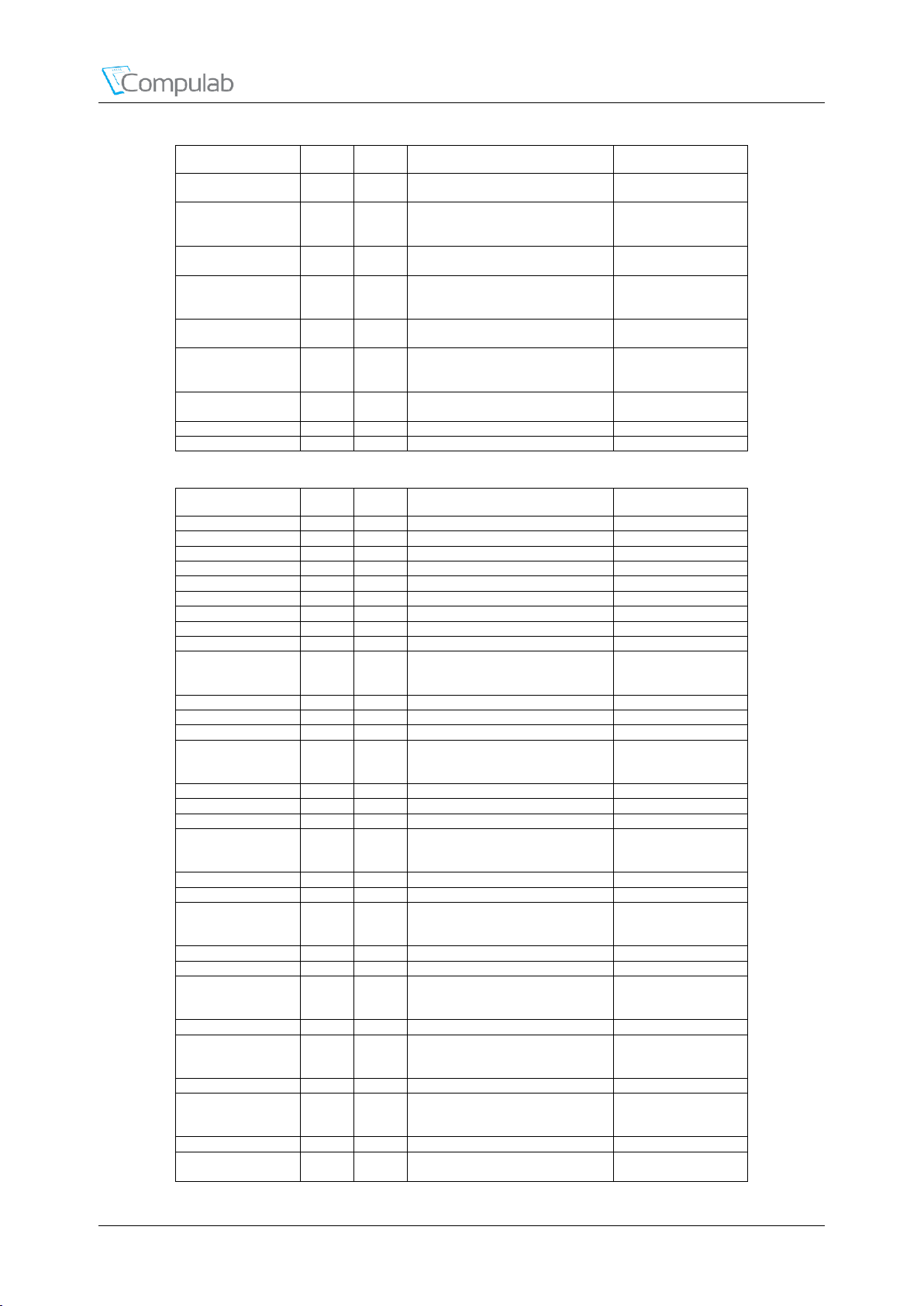
Peripheral Interfaces
Signal Name
Pin #
Type
Description
Availability
MMC1_DAT5
31*
IO
MMC/SD/SDIO Data Bus
Without "N128"
Without "N512"
MMC1_DAT5
163*
IO
MMC/SD/SDIO Data Bus
Without "N4G"
Without "N16G"
Without "N32G"
MMC1_DAT6
33*
IO
MMC/SD/SDIO Data Bus
Without "N128"
Without "N512"
MMC1_DAT6
133*
IO
MMC/SD/SDIO Data Bus
Without "N4G"
Without "N16G"
Without "N32G"
MMC1_DAT7
35*
IO
MMC/SD/SDIO Data Bus
Without "N128"
Without "N512"
MMC1_DAT7
131*
IO
MMC/SD/SDIO Data Bus
Without "N4G"
Without "N16G"
Without "N32G"
MMC1_SDCD
51*
I
SD Card Detect
Without "N128"
Without "N512"
MMC1_SDCD
201*
I
SD Card Detect
Without "A"
MMC1_SDWP
13*
I
SD Write Protect
Always
Signal Name
Pin #
Type
Description
Availability
MMC2_CLK
4*
IO
MMC/SD/SDIO Clock
Without "E1"
MMC2_CLK
39*
IO
MMC/SD/SDIO Clock
Always
MMC2_CLK
89*
IO
MMC/SD/SDIO Clock
Without "WB"
MMC2_CMD
6*
IO
MMC/SD/SDIO Command
Without "E1"
MMC2_CMD
91*
IO
MMC/SD/SDIO Command
Without "WB"
MMC2_CMD
202*
IO
MMC/SD/SDIO Command
Always
MMC2_DAT0
26*
IO
MMC/SD/SDIO Data Bus
Without "E1"
MMC2_DAT0
44*
IO
MMC/SD/SDIO Data Bus
Without "E2"
MMC2_DAT0
77*
IO
MMC/SD/SDIO Data Bus
Without "WB"
MMC2_DAT0
161*
IO
MMC/SD/SDIO Data Bus
Without "N4G"
Without "N16G"
Without "N32G"
MMC2_DAT1
14*
IO
MMC/SD/SDIO Data Bus
Without "E1"
MMC2_DAT1
36*
IO
MMC/SD/SDIO Data Bus
Without "E2"
MMC2_DAT1
79*
IO
MMC/SD/SDIO Data Bus
Without "WB"
MMC2_DAT1
163*
IO
MMC/SD/SDIO Data Bus
Without "N4G"
Without "N16G"
Without "N32G"
MMC2_DAT2
38*
IO
MMC/SD/SDIO Data Bus
Without "E2"
MMC2_DAT2
62*
IO
MMC/SD/SDIO Data Bus
Without "E1"
MMC2_DAT2
83*
IO
MMC/SD/SDIO Data Bus
Without "WB"
MMC2_DAT2
133*
IO
MMC/SD/SDIO Data Bus
Without "N4G"
Without "N16G"
Without "N32G"
MMC2_DAT3
43*
IO
MMC/SD/SDIO Data Bus
Always
MMC2_DAT3
85*
IO
MMC/SD/SDIO Data Bus
Without "WB"
MMC2_DAT3
131*
IO
MMC/SD/SDIO Data Bus
Without "N4G"
Without "N16G"
Without "N32G"
MMC2_DAT3
143*
IO
MMC/SD/SDIO Data Bus
Without "WB"
MMC2_DAT4
40*
IO
MMC/SD/SDIO Data Bus
Without "E2"
MMC2_DAT4
155*
IO
MMC/SD/SDIO Data Bus
Without "N4G"
Without "N16G"
Without "N32G"
MMC2_DAT5
47*
IO
MMC/SD/SDIO Data Bus
Without "E2"
MMC2_DAT5
153*
IO
MMC/SD/SDIO Data Bus
Without "N4G"
Without "N16G"
Without "N32G"
MMC2_DAT6
34*
IO
MMC/SD/SDIO Data Bus
Without "E2"
MMC2_DAT6
151*
IO
MMC/SD/SDIO Data Bus
Without "N4G"
Without "N16G"
Without "N32G"
MMC2_DAT7
48*
IO
MMC/SD/SDIO Data Bus
Without "E2"
MMC2_DAT7
149*
IO
MMC/SD/SDIO Data Bus
Without "N4G"
Without "N16G"
Table 21 MMC/SD/SDIO 2 Interface Signals
Revised September 2017 CM-T43 Reference Guide 31
Page 32
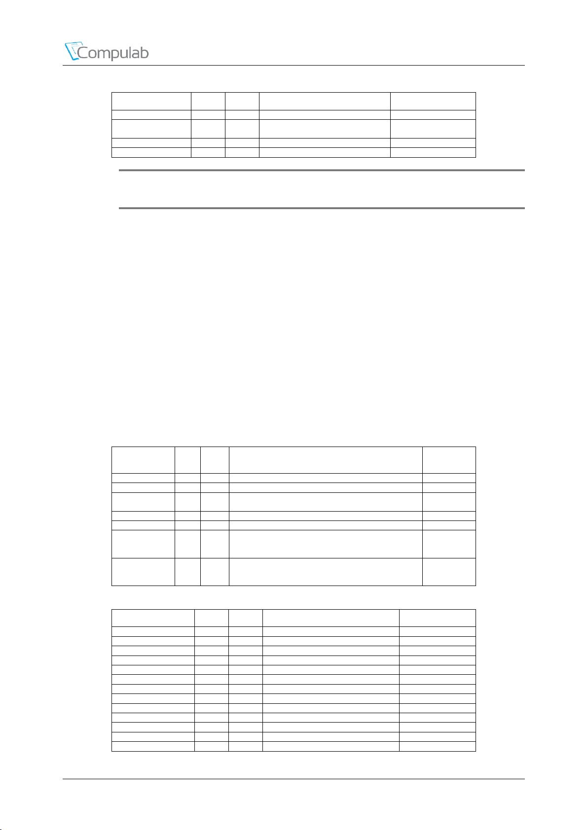
Peripheral Interfaces
Signal Name
Pin #
Type
Description
Availability
Without "N32G"
MMC2_SDCD
59*
I
SD Card Detect
Without "N128"
Without "N512"
MMC2_SDCD
197*
I
SD Card Detect
Without "A"
MMC2_SDWP
11*
I
SD Write Protect
Always
Signal Name
Pin
#
Type
Description
Availability
UART0_CTSN
7* I UART Clear to Send
Always
UART0_CTSN
94* I UART Clear to Send
Always
UART0_DCDN
77* I UART Data Carrier Detect
Without
"WB"
UART0_RTSN
9* O UART Request to Send
Always
UART0_RTSN
93* O UART Request to Send
Always
UART0_RXD
5*
I
UART Receive Data.
NOTE: Used for debug UART by default software
shipped with CM-T43
Always
UART0_TXD
3*
O
UART Transmit Data
NOTE: Used for debug UART by default software
shipped with CM-T43
Always
Signal Name
Pin #
Type
Description
Availability
UART1_CTSN
15*
IO
UART Clear to Send
Always
UART1_CTSN
89*
IO
UART Clear to Send
Without "WB"
UART1_DCDN
8* I UART Data Carrier Detect
Without "E1"
UART1_DCDN
83*
I
UART Data Carrier Detect
Without "WB"
UART1_DCDN
90*
I
UART Data Carrier Detect
Always
UART1_DSRN
24*
I
UART Data Set Ready
Without "E1"
UART1_DSRN
79*
I
UART Data Set Ready
Without "WB"
UART1_DSRN
88*
I
UART Data Set Ready
Always
UART1_DTRN
20*
O
UART Data Terminal Ready
Without "E1"
UART1_DTRN
85*
O
UART Data Terminal Ready
Without "WB"
UART1_DTRN
86*
O
UART Data Terminal Ready
Always
UART1_RIN
18*
I
UART Ring Indicator
Without "E1"
UART1_RIN
77*
I
UART Ring Indicator
Without "WB"
NOTE: Pins denoted with "*" are multifunctional. For additional details please refer to
4.10 UART
Up-to 6 UART ports are available with CM-T43. The functionality is derived from the UART
modules integrated into the Sitara AM437x SoC. The following general features are supported:
16C750 compatibility
Baud rate from 300 bps up to 3.6864 Mbps
Auto-baud between 1200 bps and 115.2 Kbps
Software/Hardware flow control (Xon/Xoff or Auto-CTS/RTS)
Modem control functions (CTS, RTS, DSR, DTR, RI, and DCD)
Support of IrDA 1.4 slow infrared (SIR), medium infrared (MIR) and fast infrared (FIR)
communications (very fast infrared (VFIR) is not supported)
Support of consumer infrared (CIR) for remote control applications
For additional details on UART, please refer to the Sitara AM437x technical reference manual. The
tables below summarize the UART interface signals
chapter 5.5 of this document
Table 22 UART0 Interface Signals
Table 23 UART1 Interface Signals
Revised September 2017 CM-T43 Reference Guide 32
Page 33
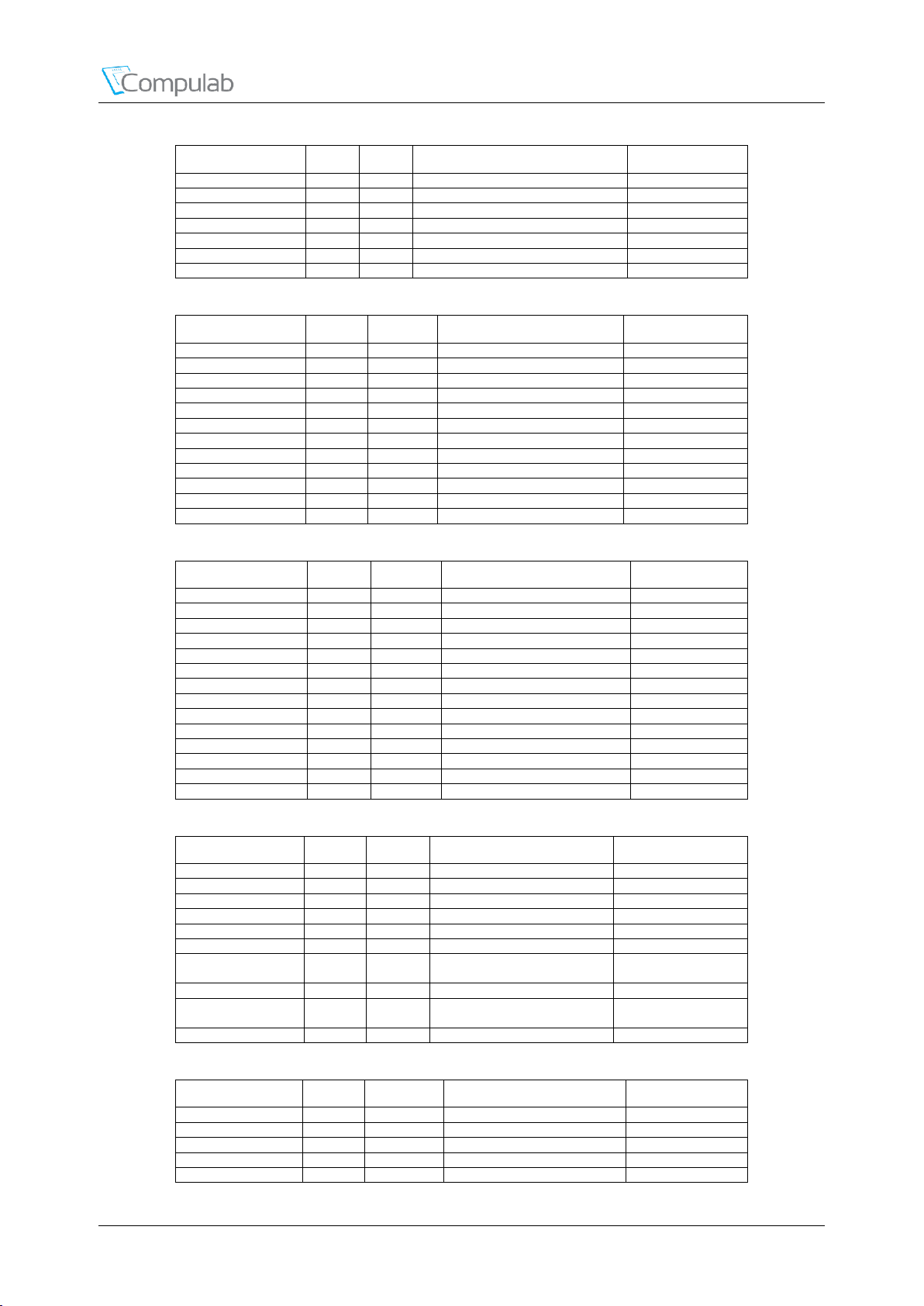
Peripheral Interfaces
Signal Name
Pin #
Type
Description
Availability
UART1_RIN
84*
I
UART Ring Indicator
Always
UART1_RTSN
17*
O
UART Request to Send
Always
UART1_RTSN
91*
O
UART Request to Send
Without "WB"
UART1_RXD
13*
IO
UART Receive Data
Always
UART1_RXD
101*
IO
UART Receive Data
Always
UART1_TXD
11*
IO
UART Transmit Data
Always
UART1_TXD
103*
IO
UART Transmit Data
Always
Signal Name
Pin #
Type
Description
Availability
UART2_CTSN
83*
IO
UART Clear to Send
Without "WB"
UART2_CTSN
124*^
IO; PD
UART Clear to Send
Always
UART2_RTSN
85*
O
UART Request to Send
Without "WB"
UART2_RTSN
126*^
O; PD
UART Request to Send
Always
UART2_RXD
8*
IO
UART Receive Data
Without "E1"
UART2_RXD
77*
IO
UART Receive Data
Without "WB"
UART2_RXD
80*
IO
UART Receive Data
Always
UART2_RXD
137*
IO
UART Receive Data
Without "WB"
UART2_TXD
24*
IO
UART Transmit Data
Without "E1"
UART2_TXD
79*
IO
UART Transmit Data
Without "WB"
UART2_TXD
82*
IO
UART Transmit Data
Always
UART2_TXD
145*
IO
UART Transmit Data
Without "WB"
Signal Name
Pin #
Type
Description
Availability
UART3_CTSN
52*
IO
UART Clear to Send
Always
UART3_CTSN
80*
IO
UART Clear to Send
Always
UART3_CTSN
128*^
IO; PD
UART Clear to Send
Always
UART3_RTSN
60*
O
UART Request to Send
Always
UART3_RTSN
82*
O
UART Request to Send
Always
UART3_RTSN
130*^
O; PD
UART Request to Send
Always
UART3_RXD
20*
IO
UART Receive Data
Without "E1"
UART3_RXD
56*
IO
UART Receive Data
Always
UART3_RXD
61*
IO
UART Receive Data
Always
UART3_RXD
86*
IO
UART Receive Data
Always
UART3_TXD
18*
IO
UART Transmit Data
Without "E1"
UART3_TXD
54*
IO
UART Transmit Data
Always
UART3_TXD
67*
IO
UART Transmit Data
Always
UART3_TXD
84*
IO
UART Transmit Data
Always
Signal Name
Pin #
Type
Description
Availability
UART4_CTSN
90*
I
UART Clear to Send
Always
UART4_CTSN
134*^
I; PD
UART Clear to Send
Always
UART4_RTSN
88*
O
UART Request to Send
Always
UART4_RTSN
136*^
O; PD
UART Request to Send
Always
UART4_RXD
7*
I
UART Receive Data
Always
UART4_RXD
14*
I
UART Receive Data
Without "E1"
UART4_RXD
51*
I
UART Receive Data
Without "N128"
Without "N512"
UART4_TXD
9*
O
UART Transmit Data
Always
UART4_TXD
59*
O
UART Transmit Data
Without "N128"
Without "N512"
UART4_TXD
62*
O
UART Transmit Data
Without "E1"
Signal Name
Pin #
Type
Description
Availability
UART5_CTSN
86*
I
UART Clear to Send
Always
UART5_CTSN
137*
I
UART Clear to Send
Without "WB"
UART5_CTSN
138*^
I; PD
UART Clear to Send
Always
UART5_RTSN
84*
O
UART Request to Send
Always
UART5_RTSN
140*^
O; PU33
UART Request to Send
Always
Table 24 UART2 Interface Signals
Table 25 UART3 Interface Signals
Table 26 UART4 Interface Signals
Revised September 2017 CM-T43 Reference Guide 33
Table 27 UART5 Interface Signals
Page 34
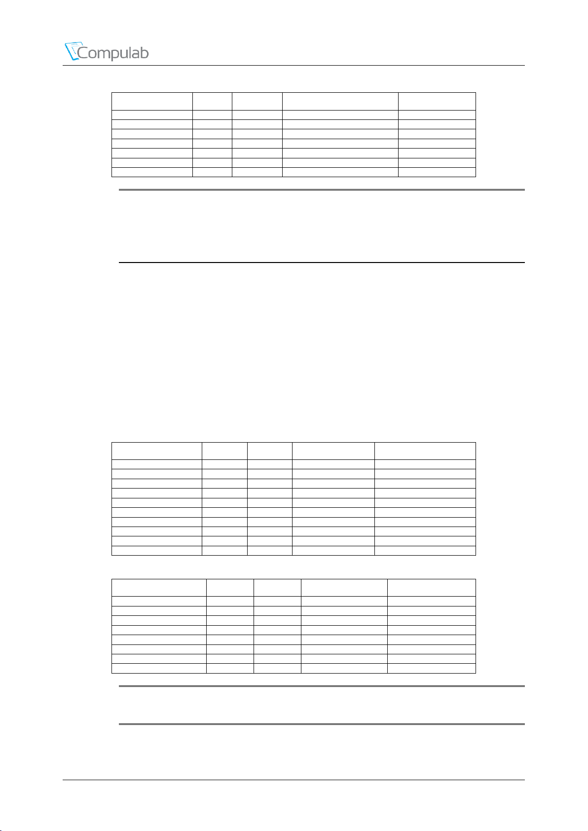
Signal Name
Pin #
Type
Description
Availability
UART5_RTSN
145*
O
UART Request to Send
Without "WB"
UART5_RXD
126*^
I; PD
UART Receive Data
Always
UART5_RXD
138*^
I; PD
UART Receive Data
Always
UART5_RXD
143*
I
UART Receive Data
Without "WB"
UART5_TXD
26*
O
UART Transmit Data
Without "E1"
UART5_TXD
124*^
O; PD
UART Transmit Data
Always
UART5_TXD
139*
O
UART Transmit Data
Without "WB"
NOTE: Pins denoted with "*" are multifunctional. For additional details please refer to
Signal Name
Pin #
Type
Description
Availability
I2C1_SCL
9*
IOD
I2C1 Clock
Always
I2C1_SCL
11*
IOD
I2C1 Clock
Always
I2C1_SCL
107*
IOD
I2C1 Clock
Always
I2C1_SCL
129*
IOD
I2C1 Clock
Always
I2C1_SCL
145*
IOD
I2C1 Clock
Without "WB"
I2C1_SDA
7*
IOD
I2C1 Data
Always
I2C1_SDA
13*
IOD
I2C1 Data
Always
I2C1_SDA
109*
IOD
I2C1 Data
Always
I2C1_SDA
135*
IOD
I2C1 Data
Always
I2C1_SDA
137*
IOD
I2C1 Data
Without "WB"
Signal Name
Pin #
Type
Description
Availability
I2C2_SCL
3*
IOD
I2C2 Clock
Always
I2C2_SCL
17*
IOD
I2C2 Clock
Always
I2C2_SCL
103*
IOD
I2C2 Clock
Always
I2C2_SCL
142*
IOD
I2C2 Clock
Always
I2C2_SDA
5*
IOD
I2C2 Data
Always
I2C2_SDA
15*
IOD
I2C2 Data
Always
I2C2_SDA
101*
IOD
I2C2 Data
Always
I2C2_SDA
144*
IOD
I2C2 Data
Always
NOTE: Pins denoted with "^" must not be pulled or driven by carrier board during SoM
4.11 I2C
CM-T43 is equipped with two I2C bus interfaces. The following general features are supported by
both I2C bus interfaces:
Compliant with Philips I2C specification version 2.1
Supports standard mode (up to 100K bits/s) and fast mode (up to 400K bits/s)
Multimaster transmitter/receiver modes (master or slave)
7-bit and 10-bit device addressing modes
For additional details on I2C, please refer to the Sitara AM437x technical reference manual. The
tables below summarize the I2C interface signals
Peripheral Interfaces
chapter 5.5 of this document
power-up / reset.
Table 28 I2C Bus 1 Interface Signals
Table 29 I2C Bus 2 Interface Signals
NOTE: Pins denoted with "*" are multifunctional. For additional details please refer to
chapter 5.5 of this document
Revised September 2017 CM-T43 Reference Guide 34
Page 35
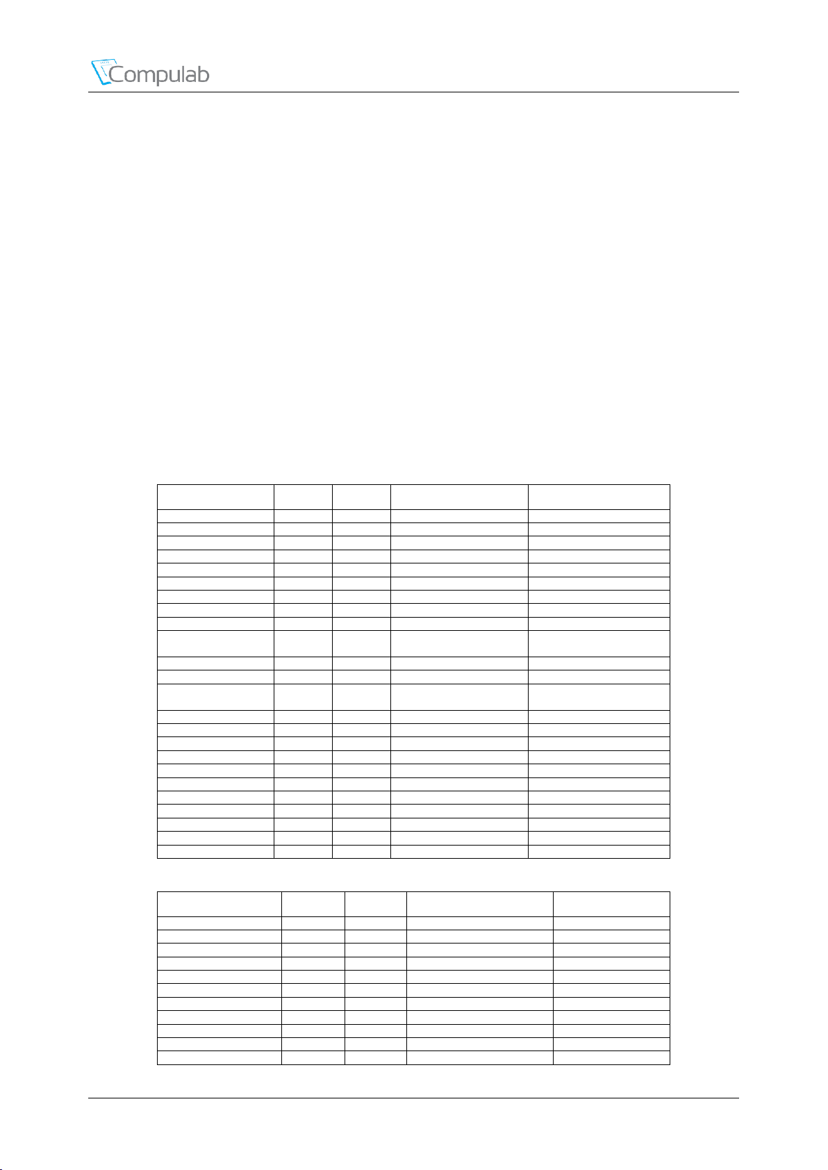
4.12 SPI
Signal Name
Pin #
Type
Description
Availability
SPI1_CS0
5*
IO
SPI Chip Select
Always
SPI1_CS0
9*
IO
SPI Chip Select
Always
SPI1_CS0
15*
IO
SPI Chip Select
Always
SPI1_CS0
125*
IO
SPI Chip Select
Always
SPI1_CS0
139*
IO
SPI Chip Select
Without "WB"
SPI1_CS1
3*
IO
SPI Chip Select
Always
SPI1_CS1
17*
IO
SPI Chip Select
Always
SPI1_CS1
67*
IO
SPI Chip Select
Always
SPI1_CS1
194*
IO
SPI Chip Select
Always
SPI1_CS2
53*
IO
SPI Chip Select
Without "N128"
Without "N512"
SPI1_CS2
113*
IO
SPI Chip Select
Always
SPI1_CS2
201*
IO
SPI Chip Select
Without "A"
SPI1_CS3
41*
IO
SPI Chip Select
Without "N128"
Without "N512"
SPI1_CS3
95*
IO
SPI Chip Select
Always
SPI1_CS3
197*
IO
SPI Chip Select
Without "A"
SPI1_D0
7*
IO
SPI Data
Always
SPI1_D0
137*
IO
SPI Data
Without "WB"
SPI1_D0
201*
IO
SPI Data
Without "A"
SPI1_D1
9*
IO
SPI Data
Always
SPI1_D1
145*
IO
SPI Data
Without "WB"
SPI1_D1
197*
IO
SPI Data
Without "A"
SPI1_SCLK
67*
IO
SPI Clock
Always
SPI1_SCLK
143*
IO
SPI Clock
Without "WB"
SPI1_SCLK
199*
IO
SPI Clock
Without "A"
Signal Name
Pin #
Type
Description
Availability
SPI2_CS0
115*
IO
SPI Chip Select
Always
SPI2_CS0
135*
IO
SPI Chip Select
Always
SPI2_CS0
144*
IO
SPI Chip Select
Always
SPI2_CS1
76*
IO
SPI Chip Select
Always
SPI2_CS1
99*
IO
SPI Chip Select
Always
SPI2_CS2
113*
IO
SPI Chip Select
Always
SPI2_CS2
142*
IO
SPI Chip Select
Always
SPI2_CS3
92*
IO
SPI Chip Select
Always
SPI2_CS3
94*
IO
SPI Chip Select
Always
SPI2_D0
93*
IO
SPI Data
Always
SPI2_D0
146*
IO
SPI Data
Always
Up-to four SPI interfaces are accessible through the CM-T43 carrier board interface. The SPI
interfaces are derived from Sitara AM437x integrated multichannel serial port interface (McSPI).
Each instance of McSPI port can operate as either a master or as an SPI slave. The following features
are supported:
Buffered receive/transmit data register per channel (1 word deep)
Full duplex / Half duplex operation
Multi-channel master or single channel slave operations
Wide selection of SPI word lengths continuous from 4 to 32 bits
Selectable clock phase and clock polarity per chip select
SPI configuration per channel (clock definition, enable polarity and word width)
Programmable 1-32 bit transmit/receive shift operations
Programmable master clock generation (operating from fixed 48-MHz functional clock input)
For additional details on McSPI, please refer to the Sitara AM437x technical reference manual. The
tables below summarize the SPI interface signals
Table 30 SPI1 Interface Signals
Peripheral Interfaces
Table 31 SPI2 Interface Signals
Revised September 2017 CM-T43 Reference Guide 35
Page 36
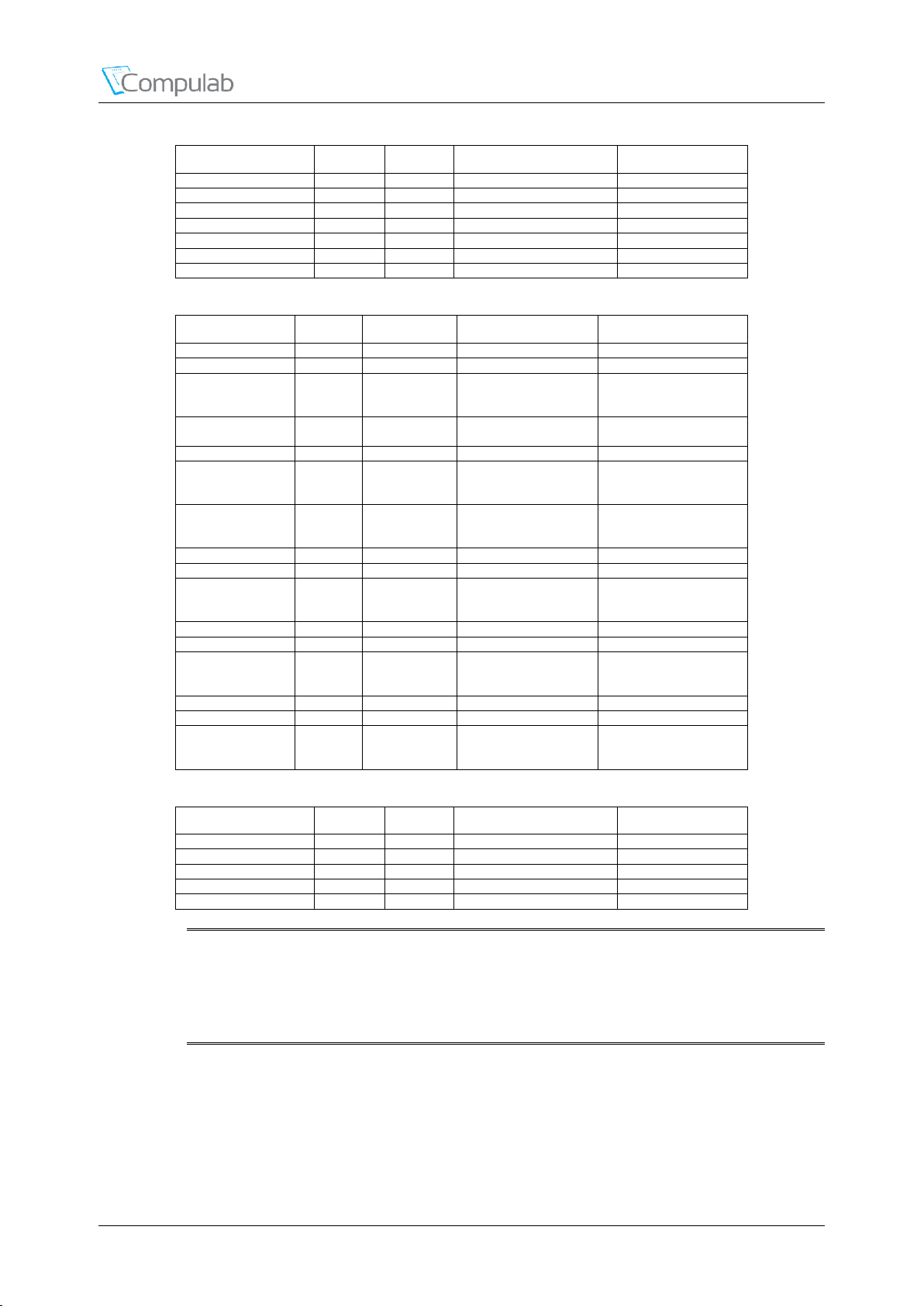
Peripheral Interfaces
Signal Name
Pin #
Type
Description
Availability
SPI2_D0
152*
IO
SPI Data
Always
SPI2_D1
74*
IO
SPI Data
Always
SPI2_D1
127*
IO
SPI Data
Always
SPI2_D1
154*
IO
SPI Data
Always
SPI2_SCLK
95*
IO
SPI Clock
Always
SPI2_SCLK
129*
IO
SPI Clock
Always
SPI2_SCLK
148*
IO
SPI Clock
Always
Signal Name
Pin #
Type
Description
Availability
SPI3_CS0
89*
IO
SPI Chip Select
Without "WB"
SPI3_CS0
140*^
IO; PU33
SPI Chip Select
Always
SPI3_CS0
149*
IO
SPI Chip Select
Without "N4G"
Without "N16G"
Without "N32G"
SPI3_CS1
41*
IO
SPI Chip Select
Without "N128"
Without "N512"
SPI3_CS1
130*^
IO; PD
SPI Chip Select
Always
SPI3_CS1
131*
IO
SPI Chip Select
Without "N4G"
Without "N16G"
Without "N32G"
SPI3_CS1
155*
IO
SPI Chip Select
Without "N4G"
Without "N16G"
Without "N32G"
SPI3_D0
101*
IO
SPI Data
Always
SPI3_D0
136*^
IO; PD
SPI Data
Always
SPI3_D0
153*
IO
SPI Data
Without "N4G"
Without "N16G"
Without "N32G"
SPI3_D1
103*
IO
SPI Data
Always
SPI3_D1
138*^
IO; PD
SPI Data
Always
SPI3_D1
151*
IO
SPI Data
Without "N4G"
Without "N16G"
Without "N32G"
SPI3_SCLK
91*
IO
SPI Clock
Without "WB"
SPI3_SCLK
134*^
IO; PD
SPI Clock
Always
SPI3_SCLK
155*
IO
SPI Clock
Without "N4G"
Without "N16G"
Without "N32G"
Signal Name
Pin #
Type
Description
Availability
SPI4_CS0
58*
IO
SPI Chip Select
Always
SPI4_CS1
52*
IO
SPI Chip Select
Always
SPI4_D0
63*
IO
SPI Data
Always
SPI4_D1
65*
IO
SPI Data
Always
SPI4_SCLK
69*
IO
SPI Clock
Always
Table 32 SPI3 Interface Signals
Table 33 SPI4 Interface Signals
NOTE: Pins denoted with "*" are multifunctional. For additional details please refer to
chapter 5.5 of this document
NOTE: Pins denoted with "^" must not be pulled or driven by carrier board during SoM
power-up / reset.
4.13 Quad SPI (QSPI)
CM-T43 is equipped with a Quad SPI interface. The interface is implemented with the Sitara
AM437x integrated QSPI controller. The following features are supported by the QSPI controller:
Programmable divider for serial data clock generation
Revised September 2017 CM-T43 Reference Guide 36
Page 37
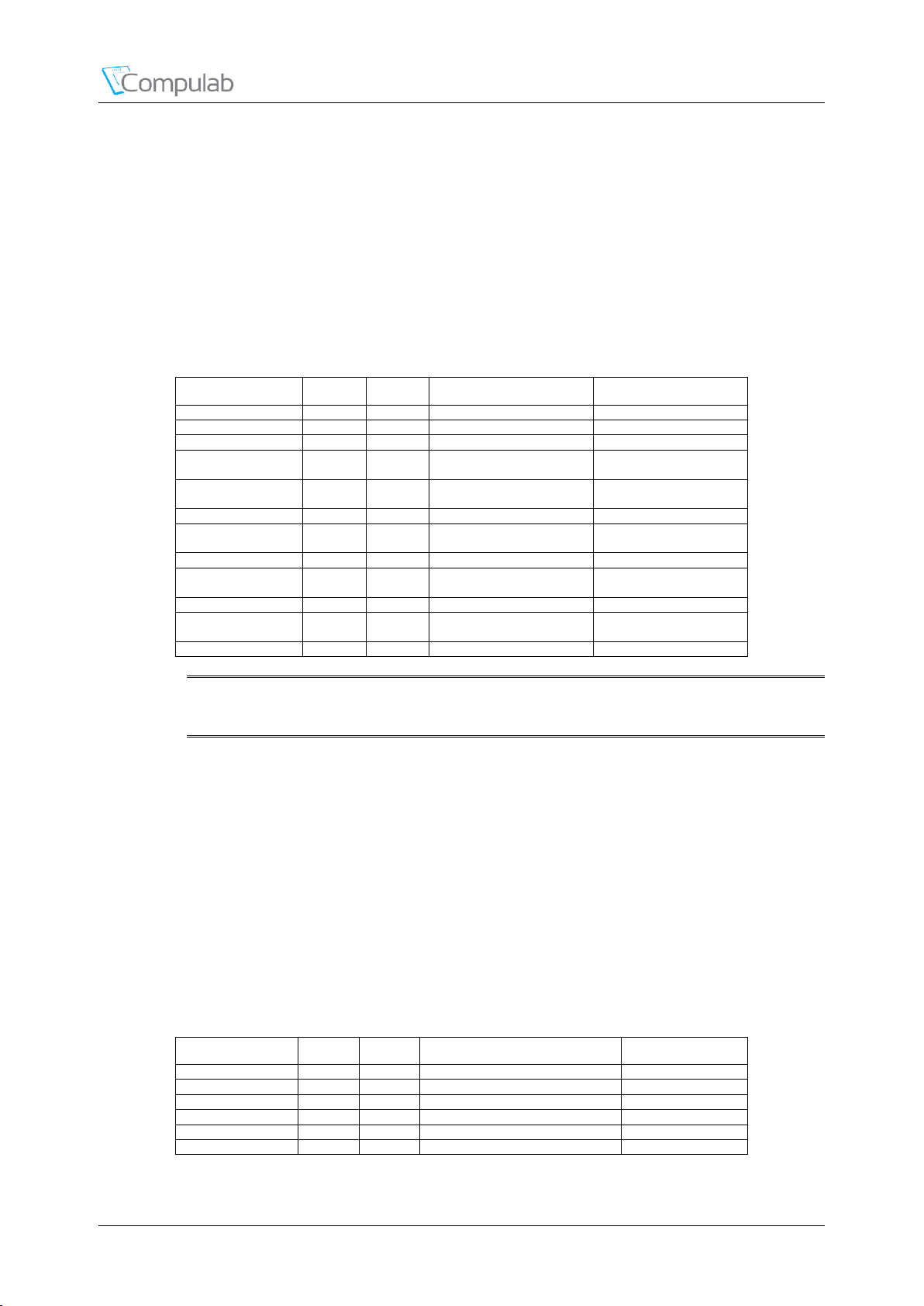
Peripheral Interfaces
Signal Name
Pin #
Type
Description
Availability
QSPI_CLK
121*
IO
QSPI Clock
Always
QSPI_CLK
202*
IO
QSPI Clock
Always
QSPI_CSN
119*
O
QSPI Chip Select
Always
QSPI_CSN
162*
O
QSPI Chip Select
Without "N128"
Without "N512"
QSPI_D0
45*
IO
QSPI Data
Without "N128"
Without "N512"
QSPI_D0
97*
IO
QSPI Data
Always
QSPI_D1
49*
I
QSPI Data
Without "N128"
Without "N512"
QSPI_D1
75*
I
QSPI Data
Always
QSPI_D2
53*
I
QSPI Data
Without "N128"
Without "N512"
QSPI_D2
73*
I
QSPI Data
Always
QSPI_D3
41*
I
QSPI Data
Without "N128"
Without "N512"
QSPI_D3
81*
I
QSPI Data
Always
Signal Name
Pin #
Type
Description
Availability
DCAN0_RX
3*
IOD
DCAN0 Receive Data
Always
DCAN0_RX
17*
IOD
DCAN0 Receive Data
Always
DCAN0_RX
62*
IOD
DCAN0 Receive Data
Without "E1"
DCAN0_TX
5*
IOD
DCAN0 Transmit Data
Always
DCAN0_TX
14*
IOD
DCAN0 Transmit Data
Without "E1"
DCAN0_TX
15*
IOD
DCAN0 Transmit Data
Always
Six pin interface (DCLK, CS_N, DOUT, DIN, QDIN1, QDIN2)
Programmable data length (No. of bits from 1-32)
Support for 3-, 4- or 6-pin SPI interface
Programmable signal polarities
Programmable active clock edge
Software controllable interface allowing for any type of SPI transfer
For additional details on QSPI, please refer to the Sitara AM437x technical reference manual. The
table below summarizes the QSPI interface signals
Table 34 QSPI Interface Signals
NOTE: Pins denoted with "*" are multifunctional. For additional details please refer to
chapter 5.5 of this document
4.14 CAN Bus
CM-T43 is equipped with two instances of the CAN bus controller. Each interface is implemented
with a Sitara AM437x integrated DCAN module. The following features are supported by the DCAN
module:
Supports CAN protocol version 2.0 part A, B (ISO 11898-1)
Bit rates up to 1 MBit/s
16, 32, 64 or 128 message objects (instantiated as 64 on this device)
DMA support
For additional details on DCAN, please refer to the Sitara AM437x technical reference manual. The
tables below summarize the CAN bus interface signals
Table 35 CAN Bus 0 Interface Signals
Revised September 2017 CM-T43 Reference Guide 37
Page 38
Peripheral Interfaces
Signal Name
Pin #
Type
Description
Availability
DCAN1_RX
9*
IOD
DCAN1 Receive Data
Always
DCAN1_RX
11*
IOD
DCAN1 Receive Data
Always
DCAN1_RX
82*
IOD
DCAN1 Receive Data
Always
DCAN1_TX
7*
IOD
DCAN1 Transmit Data
Always
DCAN1_TX
13*
IOD
DCAN1 Transmit Data
Always
DCAN1_TX
80*
IOD
DCAN1 Transmit Data
Always
Signal Name
Pin
#
Type
Description
Availability
ADC0_AIN0
66
AIO
ADC0 Analog I/O
Touchscreen controller XPUL
Always
ADC0_AIN1
68
AIO
ADC0 Analog I/O
Touchscreen controller XNUR
Always
ADC0_AIN2
70
AIO
ADC0 Analog I/O
Touchscreen controller YPLL
Always
ADC0_AIN3
72
AIO
ADC0 Analog I/O
Touchscreen controller YNLR
Always
ADC0_AIN4
175
AIO
ADC0 Analog I/O
Always
ADC0_AIN5
173
AIO
ADC0 Analog I/O
Always
ADC0_AIN6
169
AIO
ADC0 Analog I/O
Always
ADC0_AIN7
167
AIO
ADC0 Analog I/O
Always
EXT_HW_TRIGGER
99* I External Hardware Trigger for ADC conversion
Always
EXT_HW_TRIGGER
194* I External Hardware Trigger for ADC conversion
Always
Signal Name
Pin
#
Type
Description
Availability
ADC1_AIN0
166
AIO
ADC1 Analog I/O
Always
ADC1_AIN1
164
AIO
ADC1 Analog I/O
Always
ADC1_AIN2
158
AIO
ADC1 Analog I/O
Always
ADC1_AIN3
160
AIO
ADC1 Analog I/O
Always
ADC1_AIN4
188
AIO
ADC1 Analog I/O
Always
ADC1_AIN5
190
AIO
ADC1 Analog I/O
Always
ADC1_AIN6
182
AIO
ADC1 Analog I/O
Always
ADC1_AIN7
184
AIO
ADC1 Analog I/O
Always
EXT_HW_TRIGGER
99* I External Hardware Trigger for ADC conversion
Always
EXT_HW_TRIGGER
194* I External Hardware Trigger for ADC conversion
Always
Table 36 CAN Bus 1 Interface Signals
NOTE: Pins denoted with "*" are multifunctional. For additional details please refer to
chapter 5.5 of this document
4.15 ADC and Resistive Touch-Screen
CM-T43 is equipped with two instances of the general purpose ADC controller. Each instance is
implemented with a Sitara AM437x integrated ADC module. While ADC1 module can only operate
as a general purpose analog to digital converter with 8 input ports, ADC0 can also operate as a
resistive touch-screen controller, supporting 4-wire,5-wire and 8 wire touch panels. ADC0 can
operate in one of the following modes:
8 general-purpose ADC channels
4-wire TSC with 4 general-purpose ADC channels
5-wire TSC with 3 general-purpose ADC channels
8-wire TSC
For additional details on ADC, please refer to the Sitara AM437x technical reference manual. The
tables below summarize the ADC interface signals
Table 37 ADC0 Interface Signals
Table 38 ADC1 Interface Signals
Revised September 2017 CM-T43 Reference Guide 38
Page 39
Peripheral Interfaces
Signal Name
Pin #
Type
Description
Availability
HDQ_SIO
60*
IOD
HDQ 1W Data IO
Always
Signal
Name
Pin #
Type
Description
Availability
GPIO0_0
143*
IO
General purpose input/output
Without
"WB"
GPIO0_1
26*
IO
General purpose input/output
Without
"E1"
GPIO0_10
20*
IO
General purpose input/output
Without
"E1"
GPIO0_10
138*^
IO; PD
General purpose input/output
Always
GPIO0_11
18*
IO
General purpose input/output
Without
"E1"
GPIO0_11
140*^
IO; PU33
General purpose input/output
Always
NOTE: Pins denoted with "*" are multifunctional. For additional details please refer to
chapter 5.5 of this document
4.16 HDQ / 1-Wire
CM-T43 features a single instance of the HDQ/1-Wire interface. The interface is derived from the
HDQ1W module integrated into the Sitara AM437x SoC. HDQ1W supports the following features:
Software selectable HDQ or 1-Wire mode
1-Wire single-bit mode
Return-to-one accomplished via external pull-up
Interrupt to indicate Tx/Rx completion or timeout
Timeout monitor
For additional details on HDQ1W, please refer to the Sitara AM437x technical reference manual. The
table below summarizes the HDQ/1-wire interface signals
Table 39 HDQ/1-Wire Interface Signals
NOTE: Pins denoted with "*" are multifunctional. For additional details please refer to
4.17 GPIO
Up-to 133 SoC native GPIO signals are available through the carrier board interface of CM-T43. All
native GPIO signals are derived from the Sitara AM437x on-SoC GPIO modules. The GPIO pins can
be configured for the following applications:
Data input (capture)/output (drive)
Keyboard interface with a debounce cell
Interrupt generation in active mode upon the detection of external events. Detected events are
Wake-up request generation in idle mode upon the detection of external events (GPIO0_*
For additional details on GPIO modues, please refer to the Sitara AM437x technical reference
manual. The table below summarizes the GPIO interface signals
Table 40 GPIO Interface Signals
chapter 5.5 of this document
processed by two parallel independent interrupt-generation submodules to support
biprocessor operations.
only)
Revised September 2017 CM-T43 Reference Guide 39
Page 40
Peripheral Interfaces
Signal
Name
Pin #
Type
Description
Availability
GPIO0_12
15*
IO
General purpose input/output
Always
GPIO0_13
17*
IO
General purpose input/output
Always
GPIO0_14
13*
IO
General purpose input/output
Always
GPIO0_15
11*
IO
General purpose input/output
Always
GPIO0_16
14*
IO
General purpose input/output
Without
"E1"
GPIO0_17
62*
IO
General purpose input/output
Without
"E1"
GPIO0_18
198*
IO
General purpose input/output
Always
GPIO0_19
111*
IO
General purpose input/output
Always
GPIO0_19
194*
IO
General purpose input/output
Always
GPIO0_2
203*
IO
General purpose input/output
Without "A"
GPIO0_20
117*
IO
General purpose input/output
Always
GPIO0_20
152*
IO
General purpose input/output
Always
GPIO0_21
12*
IO
General purpose input/output
Without
"E1"
GPIO0_21
154*
IO
General purpose input/output
Always
GPIO0_22
129*
IO
General purpose input/output
Always
GPIO0_22
155*
IO
General purpose input/output
Without
"N4G"
Without
"N16G"
Without
"N32G"
GPIO0_23
135*
IO
General purpose input/output
Always
GPIO0_23
153*
IO
General purpose input/output
Without
"N4G"
Without
"N16G"
Without
"N32G"
GPIO0_26
151*
IO
General purpose input/output
Without
"N4G"
Without
"N16G"
Without
"N32G"
GPIO0_27
149*
IO
General purpose input/output
Without
"N4G"
Without
"N16G"
Without
"N32G"
GPIO0_28
16*
IO
General purpose input/output
Without
"E1"
GPIO0_29
139*
IO
General purpose input/output
Without
"WB"
GPIO0_3
193*
IO
General purpose input/output
Without "A"
GPIO0_30
51*
IO
General purpose input/output
Without
"N128"
Without
"N512"
GPIO0_31
59*
IO
General purpose input/output
Without
"N128"
Without
"N512"
GPIO0_4
39*
IO
General purpose input/output
Always
GPIO0_6
61*
IO
General purpose input/output
Always
GPIO0_7
67*
IO
General purpose input/output
Always
GPIO0_8
8*
IO
General purpose input/output
Without
"E1"
GPIO0_8
134*^
IO; PD
General purpose input/output
Always
GPIO0_9
24*
IO
General purpose input/output
Without
"E1"
GPIO0_9
136*^
IO; PD
General purpose input/output
Always
Revised September 2017 CM-T43 Reference Guide 40
Page 41
Peripheral Interfaces
Signal
Name
Pin #
Type
Description
Availability
GPIO1_0
21*
IO
General purpose input/output
Without
"N128"
Without
"N512"
GPIO1_1
23*
IO
General purpose input/output
Without
"N128"
Without
"N512"
GPIO1_10
5*
IO
General purpose input/output
Always
GPIO1_11
3*
IO
General purpose input/output
Always
GPIO1_12
161*
IO
General purpose input/output
Without
"N4G"
Without
"N16G"
Without
"N32G"
GPIO1_13
163*
IO
General purpose input/output
Without
"N4G"
Without
"N16G"
Without
"N32G"
GPIO1_14
133*
IO
General purpose input/output
Without
"N4G"
Without
"N16G"
Without
"N32G"
GPIO1_15
131*
IO
General purpose input/output
Without
"N4G"
Without
"N16G"
Without
"N32G"
GPIO1_16
57*
IO
General purpose input/output
Without
"E2"
GPIO1_17
44*
IO
General purpose input/output
Without
"E2"
GPIO1_18
36*
IO
General purpose input/output
Without
"E2"
GPIO1_19
38*
IO
General purpose input/output
Without
"E2"
GPIO1_2
25*
IO
General purpose input/output
Without
"N128"
Without
"N512"
GPIO1_20
30*
IO
General purpose input/output
Without
"E2"
GPIO1_21
32*
IO
General purpose input/output
Without
"E2"
GPIO1_22
40*
IO
General purpose input/output
Without
"E2"
GPIO1_23
47*
IO
General purpose input/output
Without
"E2"
GPIO1_24
34*
IO
General purpose input/output
Without
"E2"
GPIO1_25
48*
IO
General purpose input/output
Without
"E2"
GPIO1_26
50*
IO
General purpose input/output
Without
"E2"
GPIO1_27
42*
IO
General purpose input/output
Without
"E2"
GPIO1_28
43*
IO
General purpose input/output
Always
GPIO1_29
162*
IO
General purpose input/output
Without
"N128"
Without
"N512"
GPIO1_3
27*
IO
General purpose input/output
Without
"N128"
Revised September 2017 CM-T43 Reference Guide 41
Page 42
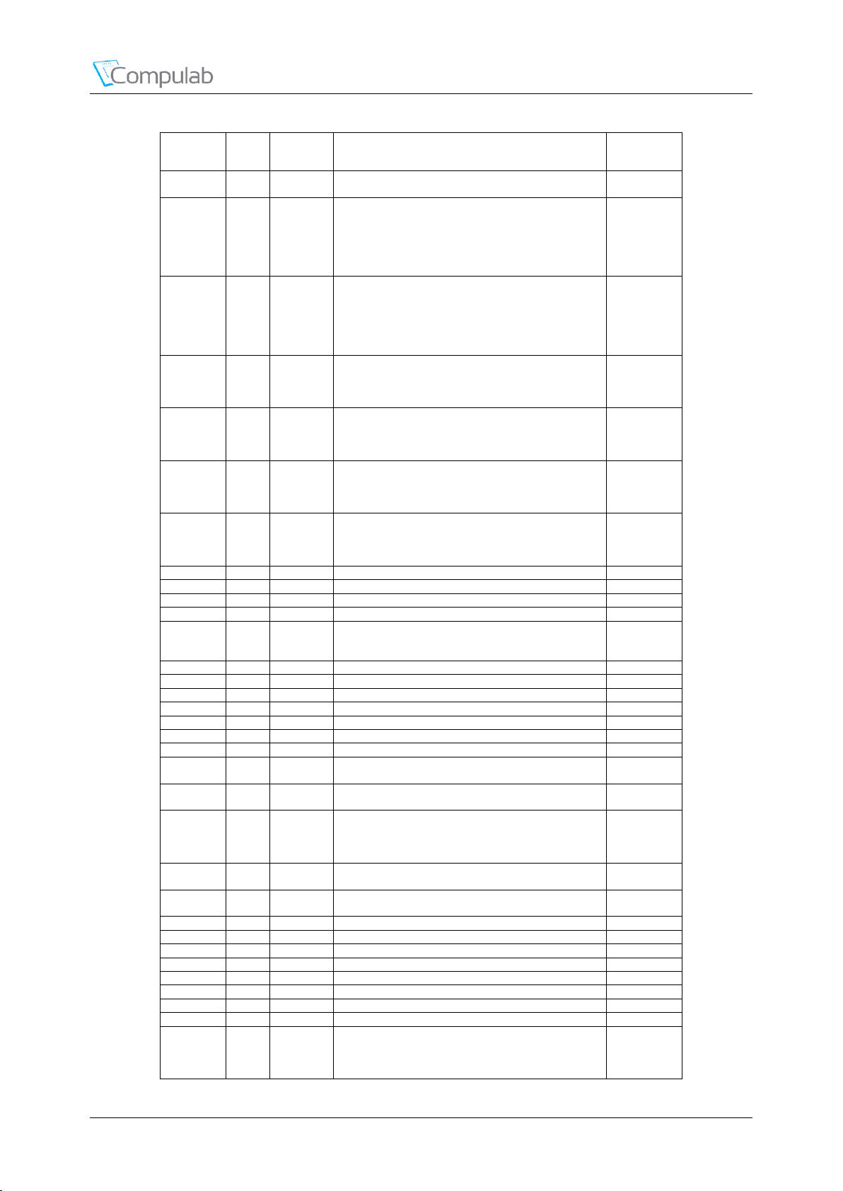
Peripheral Interfaces
Signal
Name
Pin #
Type
Description
Availability
Without
"N512"
GPIO1_30
157*
IO
General purpose input/output
Without
"N4G"
Without
"N16G"
Without
"N32G"
GPIO1_31
147*
IO
General purpose input/output
Without
"N4G"
Without
"N16G"
Without
"N32G"
GPIO1_4
29*
IO
General purpose input/output
Without
"N128"
Without
"N512"
GPIO1_5
31*
IO
General purpose input/output
Without
"N128"
Without
"N512"
GPIO1_6
33*
IO
General purpose input/output
Without
"N128"
Without
"N512"
GPIO1_7
35*
IO
General purpose input/output
Without
"N128"
Without
"N512"
GPIO1_8
7*
IO
General purpose input/output
Always
GPIO1_9
9*
IO
General purpose input/output
Always
GPIO2_0
202*
IO
General purpose input/output
Always
GPIO2_1
39*
IO
General purpose input/output
Always
GPIO2_10
116*^
IO;
PD/PU33
General purpose input/output; Pulled low/high on SoM
when normal/alternate boot sequence is selected
respectively
Always
GPIO2_11
118*^
IO; PD
General purpose input/output
Always
GPIO2_12
120*^
IO; PD
General purpose input/output
Always
GPIO2_13
122*^
IO; PD
General purpose input/output
Always
GPIO2_14
124*^
IO; PD
General purpose input/output
Always
GPIO2_15
126*^
IO; PD
General purpose input/output
Always
GPIO2_16
128*^
IO; PD
General purpose input/output
Always
GPIO2_17
130*^
IO; PD
General purpose input/output
Always
GPIO2_18
20*
IO
General purpose input/output
Without
"E1"
GPIO2_19
18*
IO
General purpose input/output
Without
"E1"
GPIO2_2
45*
IO
General purpose input/output
Without
"N128"
Without
"N512"
GPIO2_20
4*
IO
General purpose input/output
Without
"E1"
GPIO2_21
22*
IO
General purpose input/output
Without
"E1"
GPIO2_22
102*^
IO; PD
General purpose input/output
Always
GPIO2_23
100*^
IO; PD
General purpose input/output
Always
GPIO2_24
98*
IO
General purpose input/output
Always
GPIO2_25
104*^
IO; PU33
General purpose input/output
Always
GPIO2_26
90*
IO
General purpose input/output
Always
GPIO2_27
88*
IO
General purpose input/output
Always
GPIO2_28
86*
IO
General purpose input/output
Always
GPIO2_29
84*
IO
General purpose input/output
Always
GPIO2_3
49*
IO
General purpose input/output
Without
"N128"
Without
"N512"
Revised September 2017 CM-T43 Reference Guide 42
Page 43
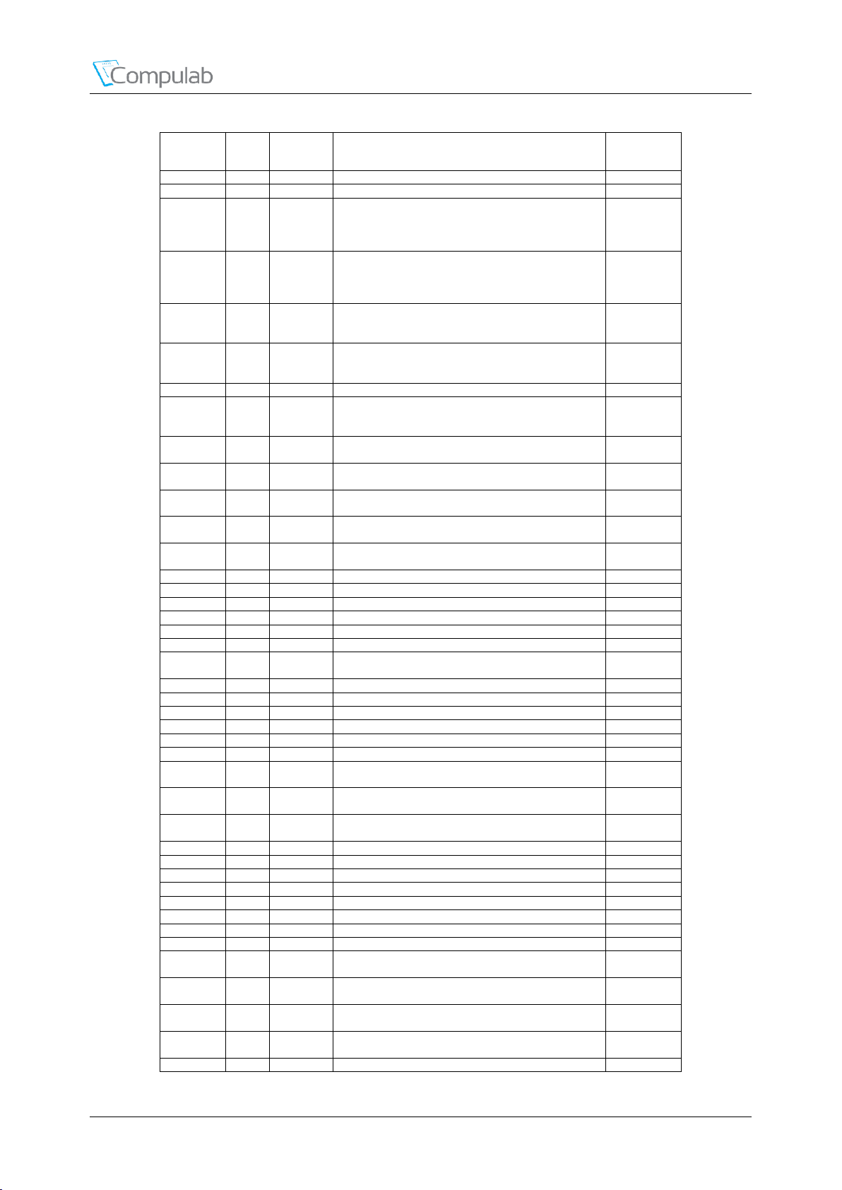
Peripheral Interfaces
Signal
Name
Pin #
Type
Description
Availability
GPIO2_30
80*
IO
General purpose input/output
Always
GPIO2_31
82*
IO
General purpose input/output
Always
GPIO2_4
53*
IO
General purpose input/output
Without
"N128"
Without
"N512"
GPIO2_5
41*
IO
General purpose input/output
Without
"N128"
Without
"N512"
GPIO2_6
106*^
IO;
PU33/PD
General purpose input/output; Pulled high/low on SoM
when normal/alternate boot sequence is selected
respectively
Always
GPIO2_7
108*^
IO;
PD/PU33
General purpose input/output; Pulled low/high on SoM
when normal/alternate boot sequence is selected
respectively
Always
GPIO2_8
110*^
IO; PD
General purpose input/output
Always
GPIO2_9
112*^
IO;
PU33/PD
General purpose input/output; Pulled high/low on SoM
when normal/alternate boot sequence is selected
respectively
Always
GPIO3_0
143*
IO
General purpose input/output
Without
"WB"
GPIO3_1
137*
IO
General purpose input/output
Without
"WB"
GPIO3_10
24*
IO
General purpose input/output
Without
"E1"
GPIO3_11
14*
IO
General purpose input/output
Without
"E1"
GPIO3_12
62*
IO
General purpose input/output
Without
"E1"
GPIO3_14
199*
IO
General purpose input/output
Without "A"
GPIO3_15
201*
IO
General purpose input/output
Without "A"
GPIO3_16
197*
IO
General purpose input/output
Without "A"
GPIO3_17
125*
IO
General purpose input/output
Always
GPIO3_18
198*
IO
General purpose input/output
Always
GPIO3_19
111*
IO
General purpose input/output
Always
GPIO3_2
145*
IO
General purpose input/output
Without
"WB"
GPIO3_20
203*
IO
General purpose input/output
Without "A"
GPIO3_21
193*
IO
General purpose input/output
Without "A"
GPIO3_22
152*
IO
General purpose input/output
Always
GPIO3_23
154*
IO
General purpose input/output
Always
GPIO3_24
129*
IO
General purpose input/output
Always
GPIO3_25
135*
IO
General purpose input/output
Always
GPIO3_3
6*
IO
General purpose input/output
Without
"E1"
GPIO3_4
26*
IO
General purpose input/output
Without
"E1"
GPIO3_9
8*
IO
General purpose input/output
Without
"E1"
GPIO4_0
76*
IO
General purpose input/output
Always
GPIO4_1
74*
IO
General purpose input/output
Always
GPIO4_10
113*
IO
General purpose input/output
Always
GPIO4_11
95*
IO
General purpose input/output
Always
GPIO4_12
99*
IO
General purpose input/output
Always
GPIO4_13
127*
IO
General purpose input/output
Always
GPIO4_14
101*
IO
General purpose input/output
Always
GPIO4_15
103*
IO
General purpose input/output
Always
GPIO4_16
89*
IO
General purpose input/output
Without
"WB"
GPIO4_17
91*
IO
General purpose input/output
Without
"WB"
GPIO4_18
77*
IO
General purpose input/output
Without
"WB"
GPIO4_19
79*
IO
General purpose input/output
Without
"WB"
GPIO4_2
148*
IO
General purpose input/output
Always
Revised September 2017 CM-T43 Reference Guide 43
Page 44
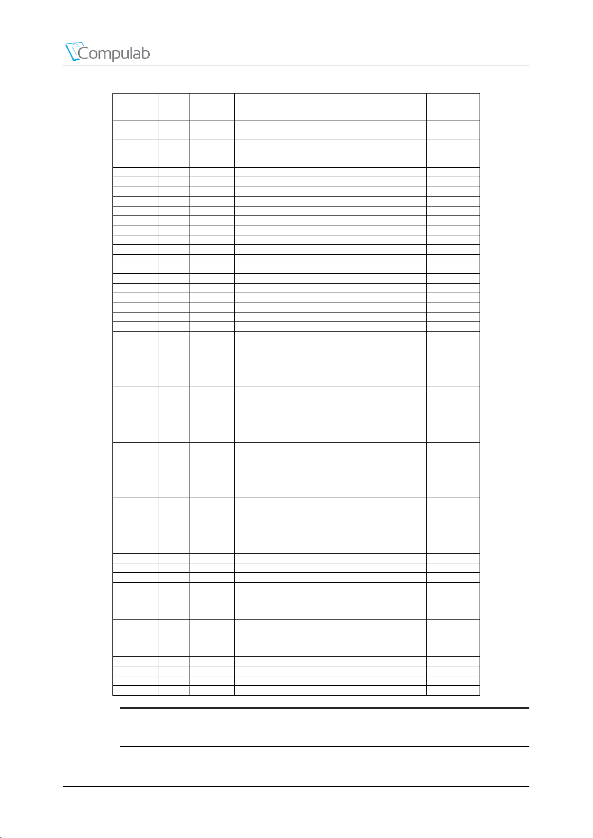
Peripheral Interfaces
Signal
Name
Pin #
Type
Description
Availability
GPIO4_20
83*
IO
General purpose input/output
Without
"WB"
GPIO4_21
85*
IO
General purpose input/output
Without
"WB"
GPIO4_24
121*
IO
General purpose input/output
Always
GPIO4_25
119*
IO
General purpose input/output
Always
GPIO4_26
97*
IO
General purpose input/output
Always
GPIO4_27
75*
IO
General purpose input/output
Always
GPIO4_28
73*
IO
General purpose input/output
Always
GPIO4_29
81*
IO
General purpose input/output
Always
GPIO4_3
146*
IO
General purpose input/output
Always
GPIO4_4
144*
IO
General purpose input/output
Always
GPIO4_5
142*
IO
General purpose input/output
Always
GPIO4_6
92*
IO
General purpose input/output
Always
GPIO4_7
94*
IO
General purpose input/output
Always
GPIO4_8
93*
IO
General purpose input/output
Always
GPIO4_9
115*
IO
General purpose input/output
Always
GPIO5_0
52*
IO
General purpose input/output
Always
GPIO5_1
60*
IO
General purpose input/output
Always
GPIO5_19
109*
IO
General purpose input/output
Always
GPIO5_2
56*
IO
General purpose input/output
Always
GPIO5_20
107*
IO
General purpose input/output
Always
GPIO5_23
149*
IO
General purpose input/output
Without
"N4G"
Without
"N16G"
Without
"N32G"
GPIO5_24
151*
IO
General purpose input/output
Without
"N4G"
Without
"N16G"
Without
"N32G"
GPIO5_25
153*
IO
General purpose input/output
Without
"N4G"
Without
"N16G"
Without
"N32G"
GPIO5_26
155*
IO
General purpose input/output
Without
"N4G"
Without
"N16G"
Without
"N32G"
GPIO5_28
194*
IO
General purpose input/output
Always
GPIO5_29
117*
IO
General purpose input/output
Always
GPIO5_3
54*
IO
General purpose input/output
Always
GPIO5_30
51*
IO
General purpose input/output
Without
"N128"
Without
"N512"
GPIO5_31
59*
IO
General purpose input/output
Without
"N128"
Without
"N512"
GPIO5_4
69*
IO
General purpose input/output
Always
GPIO5_5
63*
IO
General purpose input/output
Always
GPIO5_6
65*
IO
General purpose input/output
Always
GPIO5_7
58*
IO
General purpose input/output
Always
Revised September 2017 CM-T43 Reference Guide 44
NOTE: Pins denoted with "*" are multifunctional. For additional details please refer to
chapter 5.5 of this document
Page 45
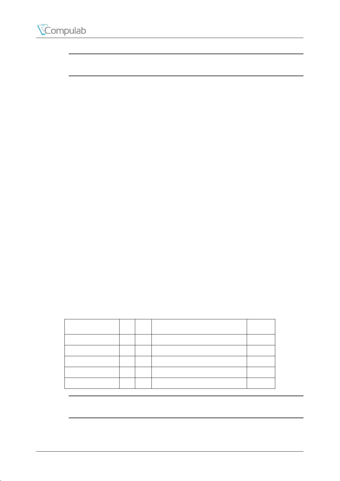
Peripheral Interfaces
Signal Name
Pin
#
Type
Description
Availability
ECAP0_IN_PWM0_OUT
67*
IO
Enhanced Capture 0 input or Auxiliary PWM0
output
Always
ECAP1_IN_PWM1_OUT
3*
IO
Enhanced Capture 1 input or Auxiliary PWM1
output
Always
ECAP1_IN_PWM1_OUT
61*
IO
Enhanced Capture 1 input or Auxiliary PWM1
output
Always
ECAP2_IN_PWM2_OUT
5*
IO
Enhanced Capture 2 input or Auxiliary PWM2
output
Always
ECAP2_IN_PWM2_OUT
125*
IO
Enhanced Capture 2 input or Auxiliary PWM2
output
Always
NOTE: Pins denoted with "^" must not be pulled or driven by carrier board during SoM
power-up / reset.
4.18 Enhanced Capture module (eCAP)
Three enhanced capture (eCAP) module instances are accessible through the CM-T43 carrier board
interface. All eCAP modules are derived from the Sitara AM437x on-SoC. eCAP can be used for the
following applications:
Sample rate measurements of audio signals
Speed measurements of rotating machinery (for example, toothed sprockets sensed via Hall
sensors)
Elapsed time measurements between position sensor pulses
Period and duty cycle measurements of pulse train signals
Decoding current or voltage amplitude derived from duty cycle encoded current/voltage
sensors
The following features are supported with eCAP:
32-bit time base counter
4-event time-stamp registers (each 32 bits)
Edge polarity selection for up to four sequenced time-stamp capture events
Interrupt on either of the four events
Single shot capture of up to four event time-stamps
Continuous mode capture of time-stamps in a four-deep circular buffer
Absolute time-stamp capture
Difference (Delta) mode time-stamp capture
All above resources dedicated to a single input pin
When not used in capture mode, the eCAP module can be configured as a single channel
PWM output
For additional details on eCAP, please refer to the Sitara AM437x technical reference manual. The
table below summarizes the eCAP interface signals
Table 41 eCAP Interface Signals
NOTE: Pins denoted with "*" are multifunctional. For additional details please refer to
chapter 5.5 of this document
Revised September 2017 CM-T43 Reference Guide 45
Page 46
Peripheral Interfaces
Signal Name
Pin #
Type
Description
Availability
EHRPWM0_SYNCI
69*
I
Sync input to eHRPWM0 module
from an external pin
Always
EHRPWM0_SYNCI
103*
I
Sync input to eHRPWM0 module
from an external pin
Always
EHRPWM0_SYNCI
125*
I
Sync input to eHRPWM0 module
from an external pin
Always
EHRPWM0_SYNCO
44*
O
Sync Output from eHRPWM0
module to an external pin
Without
"E2"
EHRPWM0_SYNCO
109*
O
Sync Output from eHRPWM0
module to an external pin
Always
EHRPWM0_SYNCO
112*^
O;
PU33/PD
Sync Output from eHRPWM0
module to an external pin; Pulled
high/low on SoM when
normal/alternate boot sequence is
selected respectively
Always
EHRPWM0_SYNCO
126*^
O; PD
Sync Output from eHRPWM0
module to an external pin
Always
EHRPWM0_SYNCO
149*
O
Sync Output from eHRPWM0
module to an external pin
Without
"N4G"
Without
"N16G"
Without
"N32G"
EHRPWM0_TRIPZONE_INPUT
65* I eHRPWM0 trip zone input
Always
EHRPWM0_TRIPZONE_INPUT
101*
I
eHRPWM0 trip zone input
Always
EHRPWM0_TRIPZONE_INPUT
197*
I
eHRPWM0 trip zone input
Without
"A"
4.19 Enhanced PWM module (eHRPWM)
Six enhanced high resolution pulse width modulator (eHRPWM) module instances are accessible
through the CM-T43 carrier board interface. All eHRPWM modules are derived from the Sitara
AM437x on-SoC. The ePWM modules are chained together via a clock synchronization scheme that
allows them to operate as a single system when required. Additionally, this synchronization scheme
can be extended to the enhanced capture peripheral modules (eCAP). eHRPWM modules can also
operate stand-alone. Each eHRPWM module supports the following features:
Dedicated 16-bit time-base counter with period and frequency control
Two PWM outputs (EPWMxA and EPWMxB) that can be used in the following
configurations:
Two independent PWM outputs with single-edge operation
Two independent PWM outputs with dual-edge symmetric operation
One independent PWM output with dual-edge asymmetric operation
Asynchronous override control of PWM signals through software.
Programmable phase-control support for lag or lead operation relative to other eHRPWM
modules
Hardware-locked (synchronized) phase relationship on a cycle-by-cycle basis
Dead-band generation with independent rising and falling edge delay control.
Programmable trip zone allocation of both cycle-by-cycle trip and one-shot trip on fault
conditions.
A trip condition can force either high, low, or high-impedance state logic levels at PWM
outputs.
Programmable event prescaling minimizes CPU overhead on interrupts.
PWM chopping by high-frequency carrier signal, useful for pulse transformer gate drives.
For additional details on eHRPWM, please refer to the Sitara AM437x technical reference manual.
The tables below summarize the eHRPWM interface signals
Table 42 eHRPWM0 Interface Signals
Revised September 2017 CM-T43 Reference Guide 46
Page 47
Peripheral Interfaces
Signal Name
Pin #
Type
Description
Availability
EHRPWM0A
115*
O
eHRPWM0 A output.
Always
EHRPWM0A
199*
O
eHRPWM0 A output.
Without
"A"
EHRPWM0B
113*
O
eHRPWM0 B output.
Always
EHRPWM0B
201*
O
eHRPWM0 B output.
Without
"A"
Signal Name
Pin #
Type
Description
Availability
EHRPWM1_TRIPZONE_INPUT
57* I eHRPWM1 trip zone input
Without "E2"
EHRPWM1_TRIPZONE_INPUT
89* I eHRPWM1 trip zone input
Without "WB"
EHRPWM1_TRIPZONE_INPUT
124*^
I; PD
eHRPWM1 trip zone input
Always
EHRPWM1_TRIPZONE_INPUT
154*
I
eHRPWM1 trip zone input
Always
EHRPWM1A
36* O eHRPWM1 A output.
Without "E2"
EHRPWM1A
73* O eHRPWM1 A output.
Always
EHRPWM1A
95* O eHRPWM1 A output.
Always
EHRPWM1A
128*^
O; PD
eHRPWM1 A output.
Always
EHRPWM1B
38* O eHRPWM1 B output.
Without "E2"
EHRPWM1B
81* O eHRPWM1 B output.
Always
EHRPWM1B
99* O eHRPWM1 B output.
Always
EHRPWM1B
130*^
O; PD
eHRPWM1 B output.
Always
Signal Name
Pin #
Type
Description
Availability
EHRPWM2_TRIPZONE_INPUT
110*^
I; PD
eHRPWM2 trip zone input
Always
EHRPWM2_TRIPZONE_INPUT
135*
I
eHRPWM2 trip zone input
Always
EHRPWM2_TRIPZONE_INPUT
151*
I
eHRPWM2 trip zone input
Without
"N4G"
Without
"N16G"
Without
"N32G"
EHRPWM2A
61* O eHRPWM2 A output.
Always
EHRPWM2A
106*^
IO;
PU33/PD
eHRPWM2 A output; Pulled
high/low on SoM when
normal/alternate boot sequence is
selected respectively
Always
EHRPWM2A
155*
O
eHRPWM2 A output.
Without
"N4G"
Without
"N16G"
Without
"N32G"
EHRPWM2B
67* O eHRPWM2 B output.
Always
EHRPWM2B
108*^
O;
PD/PU33
eHRPWM2 B output.; Pulled
low/high on SoM when
normal/alternate boot sequence is
selected respectively
Always
EHRPWM2B
153*
O
eHRPWM2 B output.
Without
"N4G"
Without
"N16G"
Without
"N32G"
Signal Name
Pin
#
Type
Description
Availability
EHRPWM3_SYNCI
63*
I
Sync input to eHRPWM3 module or
sync output to external PWM
Always
EHRPWM3_SYNCO
107*
O
Sync input to eHRPWM3 module or
sync output to external PWM
Always
EHRPWM3_TRIPZONE_INPUT
58* I eHRPWM3 trip zone input
Always
EHRPWM3A
97* O eHRPWM3 A output.
Always
EHRPWM3A
99* O eHRPWM3 A output.
Always
Table 43 eHRPWM1 Interface Signals
Table 44 eHRPWM2 Interface Signals
Revised September 2017 CM-T43 Reference Guide 47
Table 45 eHRPWM3 Interface Signals
Page 48
Peripheral Interfaces
Signal Name
Pin
#
Type
Description
Availability
EHRPWM3B
75* O eHRPWM3 B output.
Always
EHRPWM3B
127* O eHRPWM3 B output.
Always
Signal Name
Pin #
Type
Description
Availability
EHRPWM4_TRIPZONE_INPUT
129*
I
eHRPWM4 trip zone input
Always
EHRPWM4A
56* O eHRPWM4 A output.
Always
EHRPWM4B
54* O eHRPWM4 B output.
Always
Signal Name
Pin #
Type
Description
Availability
EHRPWM5_TRIPZONE_INPUT
152*
I
eHRPWM5 trip zone input
Always
EHRPWM5A
52* O eHRPWM5 A output.
Always
EHRPWM5B
60* O eHRPWM5 B output.
Always
Table 46 eHRPWM4 Interface Signals
Table 47 eHRPWM5 Interface Signals
NOTE: Pins denoted with "*" are multifunctional. For additional details please refer to
chapter 5.5 of this document
NOTE: Pins denoted with "^" must not be pulled or driven by carrier board during SoM
power-up / reset.
4.20 Quadrature Encoder Pulse module (eQEP)
Three enhanced quadrature encoder pulse (eQEP) module instances are accessible through the CMT43 carrier board interface. All eQEP modules are derived from the Sitara AM437x on-SoC. The
eQEP module allows effective sensing of wheel rotation parameters such as direction and speed
without software intervention. The eQEP inputs include two pins for quadrature-clock mode or
direction-count mode, an index (or 0 marker), and a strobe input. Each eQEP module has the
following inputs:
QEPA/XCLK and QEPB/XDIR: These two signals can be used in quadrature-clock mode or
direction-count mode
Quadrature-clock Mode: The eQEP encoders provide two square wave signals (A and B)
90 electrical degrees out of phase whose phase relationship is used to determine the
direction of rotation of the input shaft and number of eQEP pulses from the index position
to derive the relative position information. For forward or clockwise rotation, QEPA
signal leads QEPB signal and vice versa. The quadrature decoder uses these two inputs to
generate quadrature-clock and direction signals
Direction-count Mode: In direction-count mode, direction and clock signals are provided
directly from the external source. Some position encoders have this type of output instead
of quadrature output. The QEPA pin provides the clock input and the QEPB pin provides
the direction input.
QEPI: Index or Zero Marker: The eQEP encoder uses an index signal to assign an absolute
start position from which position information is incrementally encoded using quadrature
pulses. This pin is connected to the index output of the eQEP encoder to optionally reset the
position counter for each revolution. This signal can be used to initialize or latch the position
counter on the occurrence of a desired event on the index pin
QEPS: Strobe Input: This general-purpose strobe signal can initialize or latch the position
counter on the occurrence of a desired event on the strobe pin. This signal is typically
connected to a sensor or limit switch to notify that the motor has reached a defined position
Revised September 2017 CM-T43 Reference Guide 48
For additional details on eQEP, please refer to the Sitara AM437x technical reference manual. The
tables below summarize the eQEP interface signals
Page 49
Peripheral Interfaces
Signal Name
Pin #
Type
Description
Availability
EQEP0_INDEX
6*
IO
eQEP0 index.
Without "E1"
EQEP0_INDEX
203*
IO
eQEP0 index.
Without "A"
EQEP0_STROBE
4*
IO
eQEP0 strobe.
Without "E1"
EQEP0_STROBE
193*
IO
eQEP0 strobe.
Without "A"
EQEP0A_IN
12*
I
eQEP0A quadrature input
Without "E1"
EQEP0A_IN
198*
I
eQEP0A quadrature input
Always
EQEP0B_IN
16*
I
eQEP0B quadrature input
Without "E1"
EQEP0B_IN
111*
I
eQEP0B quadrature input
Always
Signal Name
Pin #
Type
Description
Availability
EQEP1_INDEX
40*
IO
eQEP1 index.
Without "E2"
EQEP1_INDEX
138*^
IO; PD
eQEP1 index.
Always
EQEP1_STROBE
47*
IO
eQEP1 strobe.
Without "E2"
EQEP1_STROBE
140*^
IO; PU33
eQEP1 strobe.
Always
EQEP1A_IN
30*
I
eQEP1A quadrature input
Without "E2"
EQEP1A_IN
134*^
I; PD
eQEP1A quadrature input
Always
EQEP1B_IN
32*
I
eQEP1B quadrature input
Without "E2"
EQEP1B_IN
136*^
I; PD
eQEP1B quadrature input
Always
Signal Name
Pin #
Type
Description
Availability
EQEP2_INDEX
120*^
IO; PD
eQEP2 index.
Always
EQEP2_INDEX
133*
IO
eQEP2 index.
Without
"N4G"
Without
"N16G"
Without
"N32G"
EQEP2_STROBE
122*^
IO; PD
eQEP2 strobe.
Always
EQEP2_STROBE
131*
IO
eQEP2 strobe.
Without
"N4G"
Without
"N16G"
Without
"N32G"
EQEP2A_IN
116*^
I;
PD/PU33
eQEP2A quadrature input; Pulled low/high on
SoM when normal/alternate boot sequence is
selected respectively
Always
EQEP2A_IN
161*
I
eQEP2A quadrature input
Without
"N4G"
Without
"N16G"
Without
"N32G"
EQEP2B_IN
118*^
I; PD
eQEP2B quadrature input
Always
EQEP2B_IN
163*
I
eQEP2B quadrature input
Without
"N4G"
Without
"N16G"
Without
"N32G"
Table 48 eQEP0 Interface Signals
Table 49 eQEP1 Interface Signals
Table 50 eQEP2 Interface Signals
NOTE: Pins denoted with "*" are multifunctional. For additional details please refer to
NOTE: Pins denoted with "^" must not be pulled or driven by carrier board during SoM
Revised September 2017 CM-T43 Reference Guide 49
chapter 5.5 of this document
power-up / reset.
Page 50
Peripheral Interfaces
Signal Name
Pin #
Type
Description
Availability
PR1_MDIO_DATA
194*
IO
MDIO Data (MUXED)
With "C1000M"
PR1_MDIO_DATA
202*
IO
MDIO Data (MUXED)
With "C1000M"
PR1_MDIO_MDCLK
39*
O
MDIO Clk (MUXED)
With "C1000M"
PR1_MDIO_MDCLK
117*
O
MDIO Clk (MUXED)
With "C1000M"
Signal Name
Pin
#
Type
Description
Availability
PR1_MII_MR0_CLK
138*
I; PD
MII Receive Clock (MUXED)
With
"C1000M"
PR1_MII_MT0_CLK
106*
IO;
PU33/PD
MII Transmit Clock (MUXED); Pulled
high/low on SoM when normal/alternate boot
sequence is selected respectively
With
"C1000M"
PR1_MII_MT0_CLK
155* I MII Transmit Clock (MUXED)
With
"C1000M"
Without
"N4G"
Without
"N16G"
Without
"N32G"
PR1_MII0_COL
153* I MII Collision Detect (MUXED)
With
"C1000M"
Without
"N4G"
Without
"N16G"
Without
"N32G"
PR1_MII0_CRS
202* I MII Carrier Sense (MUXED)
With
"C1000M"
PR1_MII0_RXD0
130*
I; PD
MII Receive Data bit 0 (MUXED)
With
"C1000M"
PR1_MII0_RXD1
128*
I; PD
MII Receive Data bit 1 (MUXED)
With
"C1000M"
PR1_MII0_RXD2
126*
I; PD
MII Receive Data bit 2 (MUXED)
With
"C1000M"
PR1_MII0_RXD3
124*
I; PD
MII Receive Data bit 3 (MUXED)
With
"C1000M"
PR1_MII0_RXDV
140*
I; PU33
MII Receive Data Valid (MUXED)
With
"C1000M"
PR1_MII0_RXER
136*
I; PD
MII Receive Data Error (MUXED)
With
"C1000M"
PR1_MII0_RXLINK
134*
I; PD
MII Receive Link (MUXED)
With
"C1000M"
PR1_MII0_TXD0
118*
O; PD
MII Transmit Data bit 0 (MUXED)
With
"C1000M"
PR1_MII0_TXD0
133* O MII Transmit Data bit 0 (MUXED)
With
"C1000M"
Without
"N4G"
4.21 PRU-ICSS
The following interfaces are a part of the PRU-ICSS block of CM-T43 Please refer to chapter 3.2 of
this document for additional details on PRU-ICSS
4.21.1 PRU-ICSS MII
CM-T43 supports industrial protocols such as EtherCAT and can operate as an EtherCAT slave
device. The EtherCAT protocol support is derived from Sitara AM437x on-SoC MII_RT module,
featuring two MII ports and configurable connections to PRUs. For additional details on PRU-ICSS
MII interface, please refer to the Sitara AM437x technical reference manual. The tables below
summarize the PRU-ICSS1 MII interface signals
Table 51 PRU-ICSS1 MII Phy Control Interface Signals
Table 52 PRU-ICSS1 MII Port 0 Interface Signals
Revised September 2017 CM-T43 Reference Guide 50
Page 51
Peripheral Interfaces
Signal Name
Pin
#
Type
Description
Availability
Without
"N16G"
Without
"N32G"
PR1_MII0_TXD1
116*
O;
PD/PU33
MII Transmit Data bit 1 (MUXED); Pulled
low/high on SoM when normal/alternate boot
sequence is selected respectively
With
"C1000M"
PR1_MII0_TXD1
163* O MII Transmit Data bit 1 (MUXED)
With
"C1000M"
Without
"N4G"
Without
"N16G"
Without
"N32G"
PR1_MII0_TXD2
112*
O;
PU33/PD
MII Transmit Data bit 2 (MUXED); Pulled
high/low on SoM when normal/alternate boot
sequence is selected respectively
With
"C1000M"
PR1_MII0_TXD2
161* O MII Transmit Data bit 2 (MUXED)
With
"C1000M"
Without
"N4G"
Without
"N16G"
Without
"N32G"
PR1_MII0_TXD3
110*
O; PD
MII Transmit Data bit 3 (MUXED)
With
"C1000M"
PR1_MII0_TXD3
149* O MII Transmit Data bit 3 (MUXED)
With
"C1000M"
Without
"N4G"
Without
"N16G"
Without
"N32G"
PR1_MII0_TXEN
108*
O;
PD/PU33
MII Transmit Enable (MUXED); Pulled
low/high on SoM when normal/alternate boot
sequence is selected respectively
With
"C1000M"
PR1_MII0_TXEN
151* O MII Transmit Enable (MUXED)
With
"C1000M"
Without
"N4G"
Without
"N16G"
Without
"N32G"
Signal Name
Pin #
Type
Description
Availability
PR1_MII_MR1_CLK
47* I MII Receive Clock (MUXED)
With "C1000M"
Without "E2"
PR1_MII_MT1_CLK
40* I MII Transmit Clock (MUXED)
With "C1000M"
Without "E2"
PR1_MII1_COL
43* I MII Collision Detect (MUXED)
With "C1000M"
PR1_MII1_CRS
39* I MII Carrier Sense (MUXED)
With "C1000M"
PR1_MII1_CRS
51* I MII Carrier Sense (MUXED)
With "C1000M"
Without "N128"
Without "N512"
PR1_MII1_RXD0
42* I MII Receive Data bit 0 (MUXED)
With "C1000M"
Without "E2"
PR1_MII1_RXD1
50* I MII Receive Data bit 1 (MUXED)
With "C1000M"
Without "E2"
PR1_MII1_RXD2
48* I MII Receive Data bit 2 (MUXED)
With "C1000M"
Without "E2"
PR1_MII1_RXD3
34* I MII Receive Data bit 3 (MUXED)
With "C1000M"
Without "E2"
Table 53 PRU-ICSS1 MII Port 1 Interface Signals
Revised September 2017 CM-T43 Reference Guide 51
Page 52
Peripheral Interfaces
Signal Name
Pin #
Type
Description
Availability
PR1_MII1_RXDV
44* I MII Receive Data Valid (MUXED)
With "C1000M"
Without "E2"
PR1_MII1_RXER
59* I MII Receive Data Error (MUXED)
With "C1000M"
Without "N128"
Without "N512"
PR1_MII1_RXLINK
41* I MII Receive Link (MUXED)
With "C1000M"
Without "N128"
Without "N512"
PR1_MII1_TXD0
32* O MII Transmit Data bit 0 (MUXED)
With "C1000M"
Without "E2"
PR1_MII1_TXD1
30* O MII Transmit Data bit 1 (MUXED)
With "C1000M"
Without "E2"
PR1_MII1_TXD2
38* O MII Transmit Data bit 2 (MUXED)
With "C1000M"
Without "E2"
PR1_MII1_TXD3
36* O MII Transmit Data bit 3 (MUXED)
With "C1000M"
Without "E2"
PR1_MII1_TXEN
57* O MII Transmit Enable (MUXED)
With "C1000M"
Without "E2"
Signal Name
Pin #
Type
Description
Availability
PR1_UART0_CTS_N
15*
I
UART Clear to Send
Always
PR1_UART0_RTS_N
17*
O
UART Request to Send
Always
PR1_UART0_RXD
13*
I
UART Receive Data
Always
PR1_UART0_TXD
11*
O
UART Transmit Data
Always
NOTE: Pins denoted with "*" are multifunctional. For additional details please refer to
chapter 5.5 of this document
4.21.2 PRU-ICSS UART
The UART peripheral within the PRU-ICSS is based on the industry standard TL16C550
asynchronous communications element, which is a functional upgrade of the TL16C450. CM-T43
carrier board interface features one instance of the PRU UART interface. For additional details on
PRU-ICSS UART, please refer to the Sitara AM437x technical reference manual. The table below
summarizes the PRU-ICSS1 UART interface signals
Table 54 PRU-ICSS1 UART Interface Signals
NOTE: Pins denoted with "*" are multifunctional. For additional details please refer to
chapter 5.5 of this document
4.21.3 PRU-ICSS Industrial Ethernet Peripheral
CM-T43 carrier board interface features one instance of the PRU-ICSS integrated “industial ethernet
peripheral” (IEP) interface. The IEP performs hardware work required for industrial ethernet
functions. The IEP module features an industrial ethernet timer with 16 compare events and a digital
I/O port (DIGIO). The industrial ethernet peripheral supports the following features:
Revised September 2017 CM-T43 Reference Guide 52
One master 32-bit count-up counter with an overflow status bit
Sixteen 32-bit compare registers
8 channel digital data input and 6 channel digital data output
Digital data out enable (optional tri-state control)
Supports direct sampling of data in signals
Data input sampling upon external latch event trough a dedicated latch input signal
For additional details on PRU-ICSS IEP, please refer to the Sitara AM437x technical reference
manual. The table below summarizes the PRU-ICSS1 industrial ethernet interface signals
Page 53
Peripheral Interfaces
Signal Name
Pin #
Type
Description
Availability
PR1_EDC_LATCH0_IN
15*
I
Data In
Always
PR1_EDC_LATCH0_IN
91*
I
Data In
Without "WB"
PR1_EDC_LATCH1_IN
17*
I
Data In
Always
PR1_EDC_LATCH1_IN
77*
I
Data In
Without "WB"
PR1_EDC_SYNC0_OUT
7* O Data Out
Always
PR1_EDC_SYNC1_OUT
9* O Data Out
Always
PR1_EDIO_DATA_IN0
83*
I
Data In
Without "WB"
PR1_EDIO_DATA_IN1
85*
I
Data In
Without "WB"
PR1_EDIO_DATA_IN2
102*^
I; PD
Data In
Always
PR1_EDIO_DATA_IN3
100*^
I; PD
Data In
Always
PR1_EDIO_DATA_IN4
98*
I
Data In
Always
PR1_EDIO_DATA_IN5
104*^
I; PU33
Data In
Always
PR1_EDIO_DATA_IN6
120*^
I; PD
Data In
Always
PR1_EDIO_DATA_IN6
157*
I
Data In
Without "N4G"
Without "N16G"
Without "N32G"
PR1_EDIO_DATA_IN7
122*^
I; PD
Data In
Always
PR1_EDIO_DATA_IN7
147*
I
Data In
Without "N4G"
Without "N16G"
Without "N32G"
PR1_EDIO_DATA_OUT2
102*^
O; PD
Data Out
Always
PR1_EDIO_DATA_OUT3
100*^
O; PD
Data Out
Always
PR1_EDIO_DATA_OUT4
98*
O
Data Out
Always
PR1_EDIO_DATA_OUT5
104*^
O; PU33
Data Out
Always
PR1_EDIO_DATA_OUT6
120*^
O; PD
Data Out
Always
PR1_EDIO_DATA_OUT6
157*
O
Data Out
Without "N4G"
Without "N16G"
Without "N32G"
PR1_EDIO_DATA_OUT7
122*^
O; PD
Data Out
Always
PR1_EDIO_DATA_OUT7
147*
O
Data Out
Without "N4G"
Without "N16G"
Without "N32G"
PR1_EDIO_LATCH_IN
79*
I
Latch In
Without "WB"
PR1_EDIO_OUTVALID
74*
O
Data Out Valid
Always
PR1_EDIO_SOF
76*
O
Start of Frame
Always
PR1_EDIO_SOF
127*
O
Start of Frame
Always
Signal Name
Pin
#
Type
Description
Availability
PR1_ECAP0_ECAP_CAPIN_APWM_O
67*
IO
Enhanced capture input or
Auxiliary PWM out
Always
PR1_ECAP0_ECAP_CAPIN_APWM_O
131*
IO
Enhanced capture input or
Auxiliary PWM out
Without
"N4G"
Without
"N16G"
Without
"N32G"
Table 55 PRU-ICSS1 Industrial Ethernet Interface Signals
NOTE: Pins denoted with "*" are multifunctional. For additional details please refer to
chapter 5.5 of this document
NOTE: Pins denoted with "^" must not be pulled or driven by carrier board during SoM
power-up / reset.
4.21.4 PRU-ICSS Industrial Capture interface (PRU-ICSS1 eCAP)
A PRU-ICSS eCAP module is available with CM-T43. The PRU ECAP module within the PRUICSS is identical to the eCAP module described in chapter 4.18 above. For additional details on PRUICSS IEP, please refer to the Sitara AM437x technical reference manual. The table below
summarizes the PRU-ICSS1 eCAP interface signals
Table 56 PRU-ICSS1 eCAP Interface Signals
Revised September 2017 CM-T43 Reference Guide 53
Page 54
Peripheral Interfaces
Signal Name
Pin #
Type
Description
Availability
PR0_PRU0_GPI0
199*
I
PRU-ICSS0 PRU0 Data In
Without "A"
PR0_PRU0_GPI1
201*
I
PRU-ICSS0 PRU0 Data In
Without "A"
PR0_PRU0_GPI10
86* I PRU-ICSS0 PRU0 Data In
Always
PR0_PRU0_GPI11
84* I PRU-ICSS0 PRU0 Data In
Always
PR0_PRU0_GPI12
80* I PRU-ICSS0 PRU0 Data In
Always
PR0_PRU0_GPI13
82* I PRU-ICSS0 PRU0 Data In
Always
PR0_PRU0_GPI14
144*
I
PRU-ICSS0 PRU0 Data In
Always
PR0_PRU0_GPI15
142*
I
PRU-ICSS0 PRU0 Data In
Always
PR0_PRU0_GPI16
92* I PRU-ICSS0 PRU0 Data In Capture Enable
Always
PR0_PRU0_GPI17
94* I PRU-ICSS0 PRU0 Data In
Always
PR0_PRU0_GPI18
56* I PRU-ICSS0 PRU0 Data In
Always
PR0_PRU0_GPI19
54* I PRU-ICSS0 PRU0 Data In
Always
PR0_PRU0_GPI2
197*
I
PRU-ICSS0 PRU0 Data In
Without "A"
PR0_PRU0_GPI3
125*
I
PRU-ICSS0 PRU0 Data In
Always
PR0_PRU0_GPI4
198*
I
PRU-ICSS0 PRU0 Data In
Always
PR0_PRU0_GPI5
111*
I
PRU-ICSS0 PRU0 Data In
Always
PR0_PRU0_GPI6
203*
I
PRU-ICSS0 PRU0 Data In
Without "A"
PR0_PRU0_GPI7
193*
I
PRU-ICSS0 PRU0 Data In
Without "A"
PR0_PRU0_GPI8
90* I PRU-ICSS0 PRU0 Data In
Always
PR0_PRU0_GPI9
88* I PRU-ICSS0 PRU0 Data In
Always
PR0_PRU0_GPO0
199*
O
PRU-ICSS0 PRU0 Data Out
Without "A"
PR0_PRU0_GPO1
201*
O
PRU-ICSS0 PRU0 Data Out
Without "A"
PR0_PRU0_GPO10
86* O PRU-ICSS0 PRU0 Data Out
Always
PR0_PRU0_GPO11
84* O PRU-ICSS0 PRU0 Data Out
Always
PR0_PRU0_GPO12
80* O PRU-ICSS0 PRU0 Data Out
Always
PR0_PRU0_GPO13
82* O PRU-ICSS0 PRU0 Data Out
Always
PR0_PRU0_GPO14
144*
O
PRU-ICSS0 PRU0 Data Out
Always
PR0_PRU0_GPO15
142*
O
PRU-ICSS0 PRU0 Data Out
Always
PR0_PRU0_GPO16
92* O PRU-ICSS0 PRU0 Data Out
Always
PR0_PRU0_GPO17
94* O PRU-ICSS0 PRU0 Data Out
Always
PR0_PRU0_GPO18
56* O PRU-ICSS0 PRU0 Data Out
Always
PR0_PRU0_GPO19
54* O PRU-ICSS0 PRU0 Data Out
Always
PR0_PRU0_GPO2
197*
O
PRU-ICSS0 PRU0 Data Out
Without "A"
PR0_PRU0_GPO3
125*
O
PRU-ICSS0 PRU0 Data Out
Always
PR0_PRU0_GPO4
198*
O
PRU-ICSS0 PRU0 Data Out
Always
PR0_PRU0_GPO5
111*
O
PRU-ICSS0 PRU0 Data Out
Always
PR0_PRU0_GPO6
203*
O
PRU-ICSS0 PRU0 Data Out
Without "A"
PR0_PRU0_GPO7
193*
O
PRU-ICSS0 PRU0 Data Out
Without "A"
PR0_PRU0_GPO8
90* O PRU-ICSS0 PRU0 Data Out
Always
PR0_PRU0_GPO9
88* O PRU-ICSS0 PRU0 Data Out
Always
PR0_PRU1_GPI0
93* I PRU-ICSS0 PRU1 Data In
Always
PR0_PRU1_GPI1
115*
I
PRU-ICSS0 PRU1 Data In
Always
PR0_PRU1_GPI10
89* I PRU-ICSS0 PRU1 Data In
Without
"WB"
PR0_PRU1_GPI11
91* I PRU-ICSS0 PRU1 Data In
Without
"WB"
PR0_PRU1_GPI12
77* I PRU-ICSS0 PRU1 Data In
Without
"WB"
PR0_PRU1_GPI13
79* I PRU-ICSS0 PRU1 Data In
Without
"WB"
PR0_PRU1_GPI14
83* I PRU-ICSS0 PRU1 Data In
Without
"WB"
PR0_PRU1_GPI15
85* I PRU-ICSS0 PRU1 Data In
Without
NOTE: Pins denoted with "*" are multifunctional. For additional details please refer to
chapter 5.5 of this document
4.21.5 PRU-ICSS GPI / GPO
CM-T43 features PRU-ICSS dedicated general purpose input / output signals. This functionality is
derived from the PRU-ICSS Enhanced GPIO submodule integrated within the Sitara AM437x. For
additional details on PRU-ICSS GPI/GPO signals, please refer to the Sitara AM437x technical
reference manual. The table below summarizes the PRU-ICSS GPI/GPO interface signals
Table 57 PRU-ICSS GPI/GPO Interface Signals
Revised September 2017 CM-T43 Reference Guide 54
Page 55
Peripheral Interfaces
Signal Name
Pin #
Type
Description
Availability
"WB"
PR0_PRU1_GPI16
109*
I
PRU-ICSS0 PRU1 Data In Capture Enable
Always
PR0_PRU1_GPI17
107*
I
PRU-ICSS0 PRU1 Data In
Always
PR0_PRU1_GPI18
52* I PRU-ICSS0 PRU1 Data In
Always
PR0_PRU1_GPI19
60* I PRU-ICSS0 PRU1 Data In
Always
PR0_PRU1_GPI2
113*
I
PRU-ICSS0 PRU1 Data In
Always
PR0_PRU1_GPI3
95* I PRU-ICSS0 PRU1 Data In
Always
PR0_PRU1_GPI4
5* I PRU-ICSS0 PRU1 Data In
Always
PR0_PRU1_GPI5
3* I PRU-ICSS0 PRU1 Data In
Always
PR0_PRU1_GPI6
102*^
I; PD
PRU-ICSS0 PRU1 Data In
Always
PR0_PRU1_GPI7
100*^
I; PD
PRU-ICSS0 PRU1 Data In
Always
PR0_PRU1_GPI8
98* I PRU-ICSS0 PRU1 Data In
Always
PR0_PRU1_GPI9
104*^
I; PU33
PRU-ICSS0 PRU1 Data In
Always
PR0_PRU1_GPO0
93* O PRU-ICSS0 PRU1 Data Out
Always
PR0_PRU1_GPO1
115*
O
PRU-ICSS0 PRU1 Data Out
Always
PR0_PRU1_GPO10
89* O PRU-ICSS0 PRU1 Data Out
Without
"WB"
PR0_PRU1_GPO11
91* O PRU-ICSS0 PRU1 Data Out
Without
"WB"
PR0_PRU1_GPO12
77* O PRU-ICSS0 PRU1 Data Out
Without
"WB"
PR0_PRU1_GPO13
79* O PRU-ICSS0 PRU1 Data Out
Without
"WB"
PR0_PRU1_GPO14
83* O PRU-ICSS0 PRU1 Data Out
Without
"WB"
PR0_PRU1_GPO15
85* O PRU-ICSS0 PRU1 Data Out
Without
"WB"
PR0_PRU1_GPO16
109*
O
PRU-ICSS0 PRU1 Data Out
Always
PR0_PRU1_GPO17
107*
O
PRU-ICSS0 PRU1 Data Out
Always
PR0_PRU1_GPO18
52* O PRU-ICSS0 PRU1 Data Out
Always
PR0_PRU1_GPO19
60* O PRU-ICSS0 PRU1 Data Out
Always
PR0_PRU1_GPO2
113*
O
PRU-ICSS0 PRU1 Data Out
Always
PR0_PRU1_GPO3
95* O PRU-ICSS0 PRU1 Data Out
Always
PR0_PRU1_GPO4
5* O PRU-ICSS0 PRU1 Data Out
Always
PR0_PRU1_GPO5
3* O PRU-ICSS0 PRU1 Data Out
Always
PR0_PRU1_GPO6
102*^
O; PD
PRU-ICSS0 PRU1 Data Out
Always
PR0_PRU1_GPO7
100*^
O; PD
PRU-ICSS0 PRU1 Data Out
Always
PR0_PRU1_GPO8
98* O PRU-ICSS0 PRU1 Data Out
Always
PR0_PRU1_GPO9
104*^
O; PU33
PRU-ICSS0 PRU1 Data Out
Always
PR1_PRU0_GPI0
106*^
IO;
PU33/PD
PRU-ICSS1 PRU0 Data In; Pulled high/low
on SoM when normal/alternate boot sequence
is selected respectively
Always
PR1_PRU0_GPI1
108*^
I;
PD/PU33
PRU-ICSS1 PRU0 Data In; Pulled low/high
on SoM when normal/alternate boot sequence
is selected respectively
Always
PR1_PRU0_GPI10
161*
I
PRU-ICSS1 PRU0 Data In
Without
"N4G"
Without
"N16G"
Without
"N32G"
PR1_PRU0_GPI11
163*
I
PRU-ICSS1 PRU0 Data In
Without
"N4G"
Without
"N16G"
Without
"N32G"
PR1_PRU0_GPI16
11* I PRU-ICSS1 PRU0 Data In Capture Enable
Always
PR1_PRU0_GPI16
13* I PRU-ICSS1 PRU0 Data In Capture Enable
Always
PR1_PRU0_GPI16
117*
I
PRU-ICSS1 PRU0 Data In Capture Enable
Always
PR1_PRU0_GPI16
133*
I
PRU-ICSS1 PRU0 Data In Capture Enable
Without
"N4G"
Without
"N16G"
Without
"N32G"
PR1_PRU0_GPI16
194*
I
PRU-ICSS1 PRU0 Data In Capture Enable
Always
PR1_PRU0_GPI2
110*^
I; PD
PRU-ICSS1 PRU0 Data In
Always
Revised September 2017 CM-T43 Reference Guide 55
Page 56
Peripheral Interfaces
Signal Name
Pin #
Type
Description
Availability
PR1_PRU0_GPI3
112*^
I;
PU33/PD
PRU-ICSS1 PRU0 Data In; Pulled high/low
on SoM when normal/alternate boot sequence
is selected respectively
Always
PR1_PRU0_GPI4
116*^
I;
PD/PU33
PRU-ICSS1 PRU0 Data In; Pulled low/high
on SoM when normal/alternate boot sequence
is selected respectively
Always
PR1_PRU0_GPI5
118*^
I; PD
PRU-ICSS1 PRU0 Data In
Always
PR1_PRU0_GPI6
120*^
I; PD
PRU-ICSS1 PRU0 Data In
Always
PR1_PRU0_GPI7
122*^
I; PD
PRU-ICSS1 PRU0 Data In
Always
PR1_PRU0_GPI8
157*
I
PRU-ICSS1 PRU0 Data In
Without
"N4G"
Without
"N16G"
Without
"N32G"
PR1_PRU0_GPI9
147*
I
PRU-ICSS1 PRU0 Data In
Without
"N4G"
Without
"N16G"
Without
"N32G"
PR1_PRU0_GPO0
106*^
IO;
PU33/PD
PRU-ICSS1 PRU0 Data Out; Pulled high/low
on SoM when normal/alternate boot sequence
is selected respectively
Always
PR1_PRU0_GPO1
108*^
O;
PD/PU33
PRU-ICSS1 PRU0 Data Out; Pulled low/high
on SoM when normal/alternate boot sequence
is selected respectively
Always
PR1_PRU0_GPO10
161*
O
PRU-ICSS1 PRU0 Data Out
Without
"N4G"
Without
"N16G"
Without
"N32G"
PR1_PRU0_GPO11
163*
O
PRU-ICSS1 PRU0 Data Out
Without
"N4G"
Without
"N16G"
Without
"N32G"
PR1_PRU0_GPO2
110*^
O; PD
PRU-ICSS1 PRU0 Data Out
Always
PR1_PRU0_GPO3
112*^
O;
PU33/PD
PRU-ICSS1 PRU0 Data Out; Pulled high/low
on SoM when normal/alternate boot sequence
is selected respectively
Always
PR1_PRU0_GPO4
116*^
O;
PD/PU33
PRU-ICSS1 PRU0 Data Out; Pulled low/high
on SoM when normal/alternate boot sequence
is selected respectively
Always
PR1_PRU0_GPO5
118*^
O; PD
PRU-ICSS1 PRU0 Data Out
Always
PR1_PRU0_GPO6
120*^
O; PD
PRU-ICSS1 PRU0 Data Out
Always
PR1_PRU0_GPO7
122*^
O; PD
PRU-ICSS1 PRU0 Data Out
Always
PR1_PRU0_GPO8
157*
O
PRU-ICSS1 PRU0 Data Out
Without
"N4G"
Without
"N16G"
Without
"N32G"
PR1_PRU0_GPO9
147*
O
PRU-ICSS1 PRU0 Data Out
Without
"N4G"
Without
"N16G"
Without
"N32G"
NOTE: Pins denoted with "*" are multifunctional. For additional details please refer to
NOTE: Pins denoted with "^" must not be pulled or driven by carrier board during SoM
Revised September 2017 CM-T43 Reference Guide 56
chapter 5.5 of this document
power-up / reset.
Page 57
Peripheral Interfaces
Signal Name
Pin #
Type
Description
Availability
TCLKIN
117*
I
Optional external clock input to all timers
Always
TIMER0
61*
IO
Timer trigger event / PWM out
Always
TIMER1
67*
IO
Timer trigger event / PWM out
Always
TIMER4
6*
IO
Timer trigger event / PWM out
Without "E1"
TIMER4
45*
IO
Timer trigger event / PWM out
Without "N128"
Without "N512"
TIMER4
194*
IO
Timer trigger event / PWM out
Always
TIMER5
17*
IO
Timer trigger event / PWM out
Always
TIMER5
41*
IO
Timer trigger event / PWM out
Without "N128"
Without "N512"
TIMER5
90*
IO
Timer trigger event / PWM out
Always
TIMER6
15*
IO
Timer trigger event / PWM out
Always
TIMER6
53*
IO
Timer trigger event / PWM out
Without "N128"
Without "N512"
TIMER6
88*
IO
Timer trigger event / PWM out
Always
TIMER7
7*
IO
Timer trigger event / PWM out
Always
TIMER7
49*
IO
Timer trigger event / PWM out
Without "N128"
Without "N512"
TIMER7
117*
IO
Timer trigger event / PWM out
Always
Signal Name
Pin #
Type
Description
Availability
CLKOUT1
194*
O
General purpose Clock output 1
Always
CLKOUT2
117*
O
General purpose Clock output 2
Always
4.22 Timers
CM-T43 features 6 instances of the Sitara AM437x integrated timer module (DMTimer). The
following main features are supported:
Counter timer with compare and capture modes
Auto-reload and Start-stop modes
16-32 bit addressing
“On the fly” read/write registers
Interrupts can be generated on overflow, compare and capture
Wake-up enable (only for Timer0)
Write posted mode
Dedicated input trigger for capture mode and dedicated output trigger/PWM signal
Dedicated output signal for general purpose use PORGPOCFG
The Timer resolution and interrupt period are dependent on the selected input clock and clock
prescaler value.
For additional details on DMTimer, please refer to the Sitara AM437x technical reference manual.
The table below summarizes the timers interface signals
Table 58 Timers Interface Signals
NOTE: Pins denoted with "*" are multifunctional. For additional details please refer to
chapter 5.5 of this document
4.23 General Purpose Clocks
CM-T43 features two software controlled general purpose clock outputs. A carrier board designer can
use these clocks for carrier board devices. For additional details on CLKOUT signals, please refer to
the Sitara AM437x technical reference manual. The table below summarizes the general purpose
clocks interface signals
Table 59 General Purpose Clocks Interface Signals
Revised September 2017 CM-T43 Reference Guide 57
Page 58
Peripheral Interfaces
Signal Name
Pin #
Type
Description
Availability
XDMA_EVENT_INTR0
194* I External DMA Event or Interrupt 0
Always
XDMA_EVENT_INTR1
117* I External DMA Event or Interrupt 1
Always
XDMA_EVENT_INTR2
61* I External DMA Event or Interrupt 2
Always
XDMA_EVENT_INTR2
67* I External DMA Event or Interrupt 2
Always
XDMA_EVENT_INTR2
139* I External DMA Event or Interrupt 2
Without "WB"
XDMA_EVENT_INTR3
93* I External DMA Event or Interrupt 3
Always
XDMA_EVENT_INTR4
115* I External DMA Event or Interrupt 4
Always
XDMA_EVENT_INTR5
113* I External DMA Event or Interrupt 5
Always
XDMA_EVENT_INTR6
95* I External DMA Event or Interrupt 6
Always
XDMA_EVENT_INTR7
99* I External DMA Event or Interrupt 7
Always
XDMA_EVENT_INTR8
127* I External DMA Event or Interrupt 8
Always
NOTE: Pins denoted with "*" are multifunctional. For additional details please refer to
chapter 5.5 of this document
4.24 External DMA/Interrupt requests
The following signals allow carrier board components to issue DMA/Interrupt requests the Sitara
AM437x SoC onboard CM-T43. For additional details on these signals please refer to the Sitara
AM437x technical reference manual. The table below summarizes the external DMA interface
signals
Table 60 External DMA Interface Signals
NOTE: Pins denoted with "*" are multifunctional. For additional details please refer to
chapter 5.5 of this document
Revised September 2017 CM-T43 Reference Guide 58
Page 59
System Logic
Signal Name
Type
Description
VSYS
PI
Main power supply. (3.3V - 5.0VTyp.).
VCC_RTC
PI
RTC back-up battery power input. Connect to a 3V coin-cell lithium battery
through a 10Ω resistor. Should be grounded if RTC functionality is not required.
GND
PI
Common ground.
Signal Name
Pin #
Type
Description
Availability
PUSH_BTN
165
I;
PUSUPPLY
Power Cycle / Wake input. A falling edge on this
signal generates a wake/power-on request to CMT43. CM-T43 power is cycled If this signal is
held low for T
p-cycle
(can be set by software to
either 8 or 15 seconds). Keeping this pin signal
constantly low results in constant power-cycling
of CM-T43 (8 or 15 seconds intervals).
Always
RTC_WAKEUP
179
I; PU18
A falling edge on this signal can be used to wake
CM-T43 from RTC only power state.
Always
AC_DET
181
I;
PUSUPPLY
Controls the power-up of the PMIC. Shorted to
GND onboard CM-T43. The PMIC powers up
whenever system power is applied.
Always
Signal Name
Pin #
Type
Description
Availability
COLD_RESET_IN
171
I;
PU33
Active low power-on-reset input. Pulled
to 3.3V through 10KΩ onboard CM-T43
Always
5 SYSTEM LOGIC
CM-T43 allows access to several system logic related signals through the carrier board interface.
Please refer to chapter 4 of this document for signal description notes and legend.
5.1 Power Supply
The CM-T43 CoM/SoM supports two power supply options:
Regulated DC supply (3.3V - 5.0V Typical).
Lithium-ion polymer battery.
CM-T43 is not equipped with an on-board battery charger. If required, such a charger must be
implemented on the carrier board.
Table 61 Power signals
5.2 Power Management
All power-management capabilities of the CM-T43 CoM/SoM are derived from the combination
of Sitara AM437x SoC with the TPS65218 PMIC. For additional details on power management
capabilities, please refer to the Sitara AM437x & TPS65218 technical reference manuals. The
following table summarizes carrier board accessible power-management signals
Table 62 Power Control signals
5.3 Reset
CM-T43 supports two reset signals: cold reset input (COLD_RESET_IN) and warm reset
input/output (SYS_nRESWARM).
Cold reset is a non-blockable reset input to the Sitara AM437x SoC, which triggers a full
logic reset to CM-T43. Cold reset is a global reset that affects every module on the device.
The cold reset assertion also causes SYS_nRESWARM assertion.
Warm reset is also a global reset, but it does not affect all the modules on the device.
Usually, the device does not require a complete reboot on a warm reset.
The COLD_RESET_IN signal should be used as the main system reset
Table 63 Reset signals
Revised September 2017 CM-T43 Reference Guide 59
Page 60
System Logic
SYS_nRESWARM
187
IO;
PU33
Active low warm reset. Pulled to 3.3V
through 10KΩ onboard CM-T43
Always
Signal Name
Pin #
Type
Description
Availability
ALT_BOOT
185
I; PD
Active high alternate boot sequence select input. Leave
floating or tie low for standard boot sequence
Always
available
sequence
ALT_BOOT
First
Second
Third
Fourth
Standard
Low or
floating
Onboard SPI Flash
(Primary storage)
Alternate
High
MMC0
USB port 1
(flash disk)
USB port 0
(serial
downloader)
Onboard SPI
Flash (Primary
storage)
5.4 Boot Sequence
CM-T43 boot sequence defines which interface/media is used by CM-T43 to load and execute the
initial software (such as U-boot). CM-T43 can load initial software from the following
interfaces/media:
The on-board primary storage device (SPI Flash with pre-flashed boot-loader).
A USB host using USB port 0 (CM-T43 acts as a USB device)
A USB flash drive using the USB port 1 (CM-T43 acts as a USB host)
An external SD/MMC card using the MMC/SD/SDIO 0 interface
CM-T43 will query boot devices/interfaces for initial software in the order defined by the active
boot sequence. A total of two different boot sequences are supported by CM-T43:
Standard sequence: Designed for normal system operation with the on-board primary
storage device as the boot media.
Alternate sequence: Designed to bypass the primary storage device. Using the alternate
sequence allows CM-T43 to boot from external devices such as USB drive and external
SD card, effectively bypassing the onboard SPI Flash.
The initial logic value of ALT_BOOT signal defines which of the supported boot sequences is
used by the system.
Table 64 Alternative Boot selection signal
Table 65 CM-T43 Boot sequences
Revised September 2017 CM-T43 Reference Guide 60
Page 61
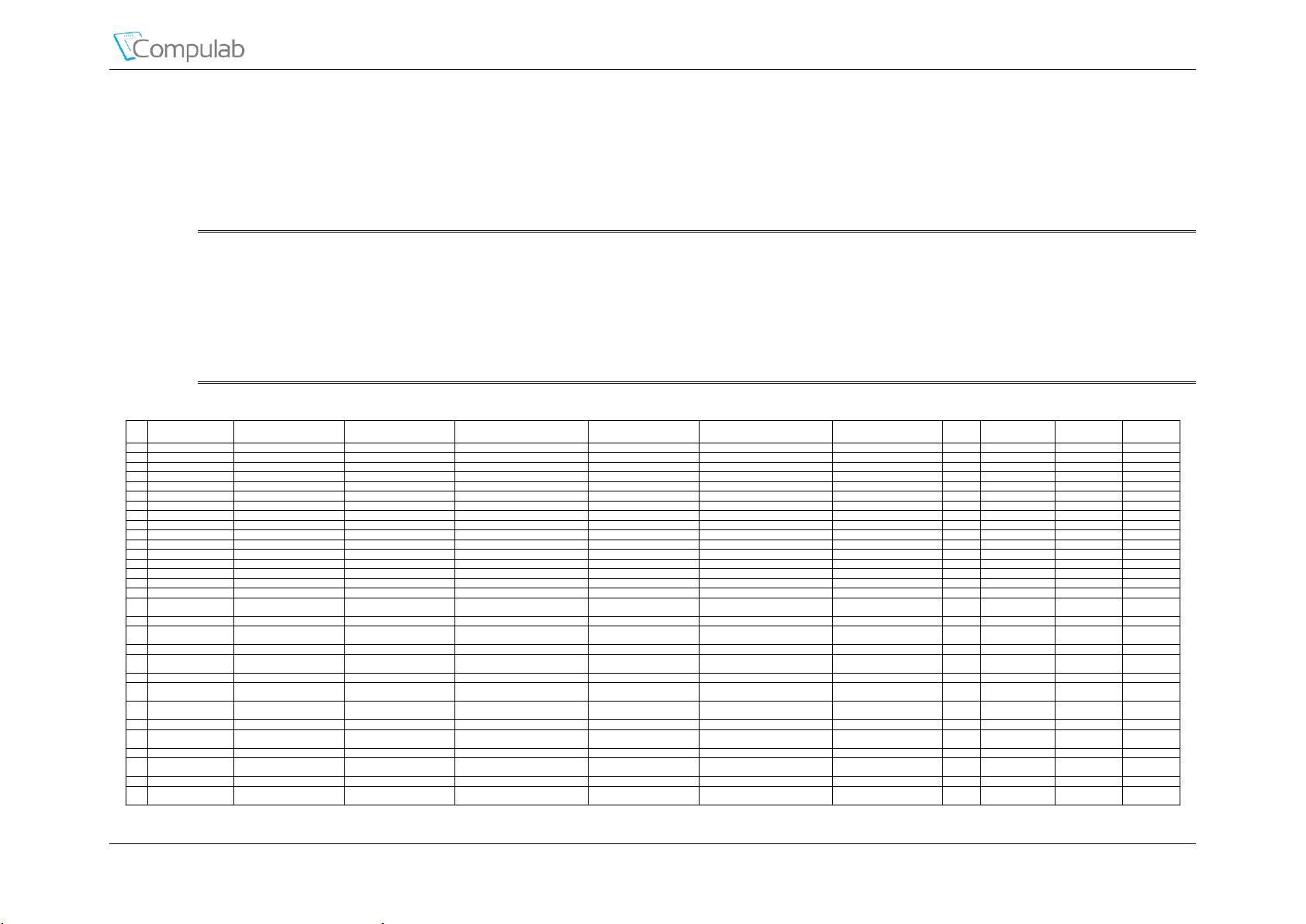
System Logic
Pin #
MODE0
MODE1
MODE2
MODE3
MODE4
MODE5
MODE6
MODE7
MODE8
MODE9
Availability
3
UART0_TXD
SPI1_CS1
DCAN0_RX
I2C2_SCL
ECAP1_IN_PWM1_OUT
PR0_PRU1_GPO5
PR0_PRU1_GPI5
GPIO1_11
Always 4 GMII1_RXD1
RMII1_RXD1
RGMII1_RD1
MCASP1_AXR3
MCASP1_FSR
EQEP0_STROBE
MMC2_CLK
GPIO2_20
Without "E1" 5 UART0_RXD
SPI1_CS0
DCAN0_TX
I2C2_SDA
ECAP2_IN_PWM2_OUT
PR0_PRU1_GPO4
PR0_PRU1_GPI4
GPIO1_10
Always 6 GMII1_TXEN
RMII1_TXEN
RGMII1_TCTL
TIMER4
MCASP1_AXR0
EQEP0_INDEX
MMC2_CMD
GPIO3_3
Without "E1" 7 UART0_CTSN
UART4_RXD
DCAN1_TX
I2C1_SDA
SPI1_D0
TIMER7
PR1_EDC_SYNC0_OUT
GPIO1_8
Always 8 GMII1_TXCLK
UART2_RXD
RGMII1_TCLK
MMC0_DAT7
MMC1_DAT0
UART1_DCDN
MCASP0_ACLKX
GPIO3_9
GPIO0_8
Without "E1" 9 UART0_RTSN
UART4_TXD
DCAN1_RX
I2C1_SCL
SPI1_D1
SPI1_CS0
PR1_EDC_SYNC1_OUT
GPIO1_9
Always
11
UART1_TXD
MMC2_SDWP
DCAN1_RX
I2C1_SCL
PR1_UART0_TXD
PR1_PRU0_GPI16
GPIO0_15
Always
12
GMII1_TXD1
RMII1_TXD1
RGMII1_TD1
MCASP1_FSR
MCASP1_AXR1
EQEP0A_IN
MMC1_CMD
GPIO0_21
Without "E1"
13
UART1_RXD
MMC1_SDWP
DCAN1_TX
I2C1_SDA
PR1_UART0_RXD
PR1_PRU0_GPI16
GPIO0_14
Always
14
GMII1_TXD3
DCAN0_TX
RGMII1_TD3
UART4_RXD
MCASP1_FSX
MMC2_DAT1
MCASP0_FSR
GPIO0_16
GPIO3_11
Without "E1"
15
UART1_CTSN
TIMER6
DCAN0_TX
I2C2_SDA
SPI1_CS0
PR1_UART0_CTS_N
PR1_EDC_LATCH0_IN
GPIO0_12
Always
16
GMII1_TXD0
RMII1_TXD0
RGMII1_TD0
MCASP1_AXR2
MCASP1_ACLKR
EQEP0B_IN
MMC1_CLK
GPIO0_28
Without "E1"
17
UART1_RTSN
TIMER5
DCAN0_RX
I2C2_SCL
SPI1_CS1
PR1_UART0_RTS_N
PR1_EDC_LATCH1_IN
GPIO0_13
Always
18
GMII1_RXD2
UART3_TXD
RGMII1_RD2
MMC0_DAT4
MMC1_DAT3
UART1_RIN
MCASP0_AXR1
GPIO2_19
GPIO0_11
Without "E1"
20
GMII1_RXD3
UART3_RXD
RGMII1_RD3
MMC0_DAT5
MMC1_DAT2
UART1_DTRN
MCASP0_AXR0
GPIO2_18
GPIO0_10
Without "E1"
21
GPMC_AD0
MMC1_DAT0
GPIO1_0
Without "N128"
Without "N512"
22
GMII1_RXD0
RMII1_RXD0
RGMII1_RD0
MCASP1_AHCLKX
MCASP1_AHCLKR
MCASP1_ACLKR
MCASP0_AXR3
GPIO2_21
Without "E1"
23
GPMC_AD1
MMC1_DAT1
GPIO1_1
Without "N128"
Without "N512"
24
GMII1_RXCLK
UART2_TXD
RGMII1_RCLK
MMC0_DAT6
MMC1_DAT1
UART1_DSRN
MCASP0_FSX
GPIO3_10
GPIO0_9
Without "E1"
25
GPMC_AD2
MMC1_DAT2
GPIO1_2
Without "N128"
Without "N512"
26
GMII1_RXDV
RGMII1_RCTL
UART5_TXD
MCASP1_ACLKX
MMC2_DAT0
MCASP0_ACLKR
GPIO3_4
GPIO0_1
Without "E1"
27
GPMC_AD3
MMC1_DAT3
GPIO1_3
Without "N128"
Without "N512"
29
GPMC_AD4
MMC1_DAT4
GPIO1_4
Without "N128"
Without "N512"
30
GPMC_A4
GMII2_TXD1
RGMII2_TD1
RMII2_TXD1
GPMC_A20
PR1_MII1_TXD1
EQEP1A_IN
GPIO1_20
Without "E2"
31
GPMC_AD5
MMC1_DAT5
GPIO1_5
Without "N128"
Without "N512"
32
GPMC_A5
GMII2_TXD0
RGMII2_TD0
RMII2_TXD0
GPMC_A21
PR1_MII1_TXD0
EQEP1B_IN
GPIO1_21
Without "E2"
33
GPMC_AD6
MMC1_DAT6
GPIO1_6
Without "N128"
Without "N512"
34
GPMC_A8
GMII2_RXD3
RGMII2_RD3
MMC2_DAT6
GPMC_A24
PR1_MII1_RXD3
MCASP0_ACLKX
GPIO1_24
Without "E2"
35
GPMC_AD7
MMC1_DAT7
GPIO1_7
Without "N128"
Without "N512"
5.5 Signal Multiplexing Characteristics
Up to 145 of the CM-T43 carrier board interface pins are multifunctional. Multifunctional pins enable extensive functional flexibility of the CM-T43
CoM/SoM by allowing usage of a single carrier board interface pin for one of several functions. Up-to 10 functions (MUX modes) are accessible through each
multifunctional carrier board interface pin. The multifunctional capabilities of CM-T43 pins are derived from the Sitara AM437x SoC control module
NOTE: Pin function selection is controlled by software.
NOTE: Each pin can be used for a single function at a time.
NOTE: Only one pin can be used for each function (in case a function is available on more than one carrier board interface pin).
NOTE: An empty MUX mode is a “RESERVED” function and must not be used.
Table 66 Multifunctional Signals
Revised September 2017 CM-T43 Reference Guide 61
Page 62
System Logic
Pin #
MODE0
MODE1
MODE2
MODE3
MODE4
MODE5
MODE6
MODE7
MODE8
MODE9
Availability
36
GPMC_A2
GMII2_TXD3
RGMII2_TD3
MMC2_DAT1
GPMC_A18
PR1_MII1_TXD3
EHRPWM1A
GPIO1_18
Without "E2"
38
GPMC_A3
GMII2_TXD2
RGMII2_TD2
MMC2_DAT2
GPMC_A19
PR1_MII1_TXD2
EHRPWM1B
GPIO1_19
Without "E2"
39
GPMC_CLK
GPMC_WAIT1
MMC2_CLK
PR1_MII1_CRS
PR1_MDIO_MDCLK
MCASP0_FSR
GPIO2_1
GPIO0_4
Always
40
GPMC_A6
GMII2_TXCLK
RGMII2_TCLK
MMC2_DAT4
GPMC_A22
PR1_MII_MT1_CLK
EQEP1_INDEX
GPIO1_22
Without "E2"
41
GPMC_BE0N_CLE
SPI1_CS3
TIMER5
QSPI_D3
PR1_MII1_RXLINK
GPMC_A5
SPI3_CS1
GPIO2_5
Without "N128"
Without "N512"
42
GPMC_A11
GMII2_RXD0
RGMII2_RD0
RMII2_RXD0
GPMC_A27
PR1_MII1_RXD0
MCASP0_AXR1
GPIO1_27
Without "E2"
43
GPMC_BE1N
GMII2_COL
GPMC_CSN6
MMC2_DAT3
GPMC_DIR
PR1_MII1_COL
MCASP0_ACLKR
GPIO1_28
Always
44
GPMC_A1
GMII2_RXDV
RGMII2_RCTL
MMC2_DAT0
GPMC_A17
PR1_MII1_RXDV
EHRPWM0_SYNCO
GPIO1_17
Without "E2"
45
GPMC_ADVN_ALE
SPI0_CS3
TIMER4
QSPI_D0
GPIO2_2
Without "N128"
Without "N512"
47
GPMC_A7
GMII2_RXCLK
RGMII2_RCLK
MMC2_DAT5
GPMC_A23
PR1_MII_MR1_CLK
EQEP1_STROBE
GPIO1_23
Without "E2"
48
GPMC_A9
GMII2_RXD2
RGMII2_RD2
MMC2_DAT7
GPMC_A25
PR1_MII1_RXD2
MCASP0_FSX
GPIO1_25
RMII2_CRS_DV
Without "E2"
49
GPMC_OEN_REN
SPI0_CS2
TIMER7
QSPI_D1
GPIO2_3
Without "N128"
Without "N512"
50
GPMC_A10
GMII2_RXD1
RGMII2_RD1
RMII2_RXD1
GPMC_A26
PR1_MII1_RXD1
MCASP0_AXR0
GPIO1_26
Without "E2"
51
GPMC_WAIT0
GMII2_CRS
GPMC_CSN4
RMII2_CRS_DV
MMC1_SDCD
PR1_MII1_CRS
UART4_RXD
GPIO0_30
GPIO5_30
Without "N128"
Without "N512"
52
UART3_CTSN
SPI4_CS1
PR0_PRU1_GPO18
PR0_PRU1_GPI18
EHRPWM5A
GPIO5_0
Always
53
GPMC_WEN
SPI1_CS2
TIMER6
QSPI_D2
GPIO2_4
Without "N128"
Without "N512"
54
UART3_TXD
PR0_PRU0_GPO19
PR0_PRU0_GPI19
EHRPWM4B
GPIO5_3
Always
56
UART3_RXD
PR0_PRU0_GPO18
PR0_PRU0_GPI18
EHRPWM4A
GPIO5_2
Always
57
GPMC_A0
GMII2_TXEN
RGMII2_TCTL
RMII2_TXEN
GPMC_A16
PR1_MII1_TXEN
EHRPWM1_TRIPZONE_INPUT
GPIO1_16
Without "E2"
58
SPI4_CS0
EHRPWM3_TRIPZONE_INPUT
GPIO5_7
Always
59
GPMC_WPN
GMII2_RXER
GPMC_CSN5
RMII2_RXER
MMC2_SDCD
PR1_MII1_RXER
UART4_TXD
GPIO0_31
GPIO5_31
Without "N128"
Without "N512"
60
UART3_RTSN
HDQ_SIO
PR0_PRU1_GPO19
PR0_PRU1_GPI19
EHRPWM5B
GPIO5_1
Always
61
SPI0_CS1
UART3_RXD
ECAP1_IN_PWM1_OUT
MMC0_POW
XDMA_EVENT_INTR2
MMC0_SDCD
EMU4
GPIO0_6
EHRPWM2A
TIMER0
Always
62
GMII1_TXD2
DCAN0_RX
RGMII1_TD2
UART4_TXD
MCASP1_AXR0
MMC2_DAT2
MCASP0_AHCLKX
GPIO0_17
GPIO3_12
Without "E1"
63
SPI4_D0
EHRPWM3_SYNCI
GPIO5_5
Always
65
SPI4_D1
EHRPWM0_TRIPZONE_INPUT
GPIO5_6
Always
67
ECAP0_IN_PWM0_OUT
UART3_TXD
SPI1_CS1
PR1_ECAP0_ECAP_CAPIN_APWM_O
SPI1_SCLK
MMC0_SDWP
XDMA_EVENT_INTR2
GPIO0_7
EHRPWM2B
TIMER1
Always
69
SPI4_SCLK
EHRPWM0_SYNCI
GPIO5_4
Always
73
CAM0_DATA6
MMC1_DAT2
QSPI_D2
EHRPWM1A
GPIO4_28
Always
74
CAM0_VD
DSS_DATA22
PR1_EDIO_OUTVALID
SPI2_D1
EMU11
EMU3
GPIO4_1
Always
75
CAM0_DATA5
MMC1_DAT1
QSPI_D1
EHRPWM3B
GPIO4_27
Always
76
CAM0_HD
DSS_DATA23
PR1_EDIO_SOF
SPI2_CS1
EMU10
EMU2
GPIO4_0
Always
77
CAM1_DATA4
UART1_RIN
UART2_RXD
MMC2_DAT0
PR0_PRU1_GPO12
PR0_PRU1_GPI12
PR1_EDC_LATCH1_IN
GPIO4_18
UART0_DCDN
Without "WB"
79
CAM1_DATA5
UART1_DSRN
UART2_TXD
MMC2_DAT1
PR0_PRU1_GPO13
PR0_PRU1_GPI13
PR1_EDIO_LATCH_IN
GPIO4_19
Without "WB"
80
MMC0_CLK
GPMC_A24
UART3_CTSN
UART2_RXD
DCAN1_TX
PR0_PRU0_GPO12
PR0_PRU0_GPI12
GPIO2_30
Always
81
CAM0_DATA7
MMC1_DAT3
QSPI_D3
EHRPWM1B
GPIO4_29
Always
82
MMC0_CMD
GPMC_A25
UART3_RTSN
UART2_TXD
DCAN1_RX
PR0_PRU0_GPO13
PR0_PRU0_GPI13
GPIO2_31
Always
83
CAM1_DATA6
UART1_DCDN
UART2_CTSN
MMC2_DAT2
PR0_PRU1_GPO14
PR0_PRU1_GPI14
PR1_EDIO_DATA_IN0
GPIO4_20
Without "WB"
84
MMC0_DAT0
GPMC_A23
UART5_RTSN
UART3_TXD
UART1_RIN
PR0_PRU0_GPO11
PR0_PRU0_GPI11
GPIO2_29
Always
85
CAM1_DATA7
UART1_DTRN
UART2_RTSN
MMC2_DAT3
PR0_PRU1_GPO15
PR0_PRU1_GPI15
PR1_EDIO_DATA_IN1
GPIO4_21
Without "WB"
86
MMC0_DAT1
GPMC_A22
UART5_CTSN
UART3_RXD
UART1_DTRN
PR0_PRU0_GPO10
PR0_PRU0_GPI10
GPIO2_28
Always
88
MMC0_DAT2
GPMC_A21
UART4_RTSN
TIMER6
UART1_DSRN
PR0_PRU0_GPO9
PR0_PRU0_GPI9
GPIO2_27
Always
89
CAM1_DATA2
UART1_CTSN
SPI3_CS0
MMC2_CLK
PR0_PRU1_GPO10
PR0_PRU1_GPI10
EHRPWM1_TRIPZONE_INPUT
GPIO4_16
Without "WB"
90
MMC0_DAT3
GPMC_A20
UART4_CTSN
TIMER5
UART1_DCDN
PR0_PRU0_GPO8
PR0_PRU0_GPI8
GPIO2_26
Always
91
CAM1_DATA3
UART1_RTSN
SPI3_SCLK
MMC2_CMD
PR0_PRU1_GPO11
PR0_PRU1_GPI11
PR1_EDC_LATCH0_IN
GPIO4_17
Without "WB"
92
CAM0_DATA9
DSS_DATA17
PR0_PRU0_GPO16
SPI2_CS3
PR0_PRU0_GPI16
EMU8
GPIO4_6
Always
93
CAM1_DATA8
XDMA_EVENT_INTR3
SPI0_CS2
PR0_PRU1_GPO0
SPI2_D0
PR0_PRU1_GPI0
EMU10
GPIO4_8
UART0_RTSN
Always
94
CAM1_DATA9
DSS_DATA16
PR0_PRU0_GPO17
SPI2_CS3
PR0_PRU0_GPI17
EMU9
GPIO4_7
UART0_CTSN
Always
95
CAM1_PCLK
XDMA_EVENT_INTR6
SPI1_CS3
PR0_PRU1_GPO3
SPI2_SCLK
PR0_PRU1_GPI3
EHRPWM1A
GPIO4_11
Always
97
CAM0_DATA4
MMC1_DAT0
CAM1_WEN
QSPI_D0
EHRPWM3A
GPIO4_26
Always
98
DSS_PCLK
GPMC_A10
GPMC_A3
PR1_EDIO_DATA_IN4
PR1_EDIO_DATA_OUT4
PR0_PRU1_GPO8
PR0_PRU1_GPI8
GPIO2_24
Always
99
CAM1_FIELD
XDMA_EVENT_INTR7
EXT_HW_TRIGGER
CAM0_DATA10
SPI2_CS1
CAM1_DATA10
EHRPWM1B
GPIO4_12
EHRPWM3A
Always
100
DSS_HSYNC
GPMC_A9
GPMC_A2
PR1_EDIO_DATA_IN3
PR1_EDIO_DATA_OUT3
PR0_PRU1_GPO7
PR0_PRU1_GPI7
GPIO2_23
Always
101
CAM1_DATA0
UART1_RXD
SPI3_D0
I2C2_SDA
EHRPWM0_TRIPZONE_INPUT
GPIO4_14
Always
102
DSS_VSYNC
GPMC_A8
GPMC_A1
PR1_EDIO_DATA_IN2
PR1_EDIO_DATA_OUT2
PR0_PRU1_GPO6
PR0_PRU1_GPI6
GPIO2_22
Always
103
CAM1_DATA1
UART1_TXD
SPI3_D1
I2C2_SCL
EHRPWM0_SYNCI
GPIO4_15
Always
104
DSS_AC_BIAS_EN
GPMC_A11
GPMC_A4
PR1_EDIO_DATA_IN5
PR1_EDIO_DATA_OUT5
PR0_PRU1_GPO9
PR0_PRU1_GPI9
GPIO2_25
Always
106
DSS_DATA0
GPMC_A0
PR1_MII_MT0_CLK
EHRPWM2A
PR1_PRU0_GPO0
PR1_PRU0_GPI0
GPIO2_6
Always
107
CAM0_DATA1
CAM1_DATA8
I2C1_SCL
PR0_PRU1_GPO17
PR0_PRU1_GPI17
EHRPWM3_SYNCO
GPIO5_20
Always
108
DSS_DATA1
GPMC_A1
PR1_MII0_TXEN
EHRPWM2B
PR1_PRU0_GPO1
PR1_PRU0_GPI1
GPIO2_7
Always
109
CAM0_DATA0
CAM1_DATA9
I2C1_SDA
PR0_PRU1_GPO16
PR0_PRU1_GPI16
EHRPWM0_SYNCO
GPIO5_19
Always
110
DSS_DATA2
GPMC_A2
PR1_MII0_TXD3
EHRPWM2_TRIPZONE_INPUT
PR1_PRU0_GPO2
PR1_PRU0_GPI2
GPIO2_8
Always
111
MCASP0_FSR
EQEP0B_IN
MCASP0_AXR3
MCASP1_FSX
EMU2
PR0_PRU0_GPO5
PR0_PRU0_GPI5
GPIO3_19
GPIO0_19
Always
112
DSS_DATA3
GPMC_A3
PR1_MII0_TXD2
EHRPWM0_SYNCO
PR1_PRU0_GPO3
PR1_PRU0_GPI3
GPIO2_9
Always
Revised September 2017 CM-T43 Reference Guide 62
Page 63
System Logic
Pin #
MODE0
MODE1
MODE2
MODE3
MODE4
MODE5
MODE6
MODE7
MODE8
MODE9
Availability
113
CAM1_VD
XDMA_EVENT_INTR5
SPI1_CS2
PR0_PRU1_GPO2
SPI2_CS2
PR0_PRU1_GPI2
EHRPWM0B
GPIO4_10
Always
115
CAM1_HD
XDMA_EVENT_INTR4
SPI0_CS3
PR0_PRU1_GPO1
SPI2_CS0
PR0_PRU1_GPI1
EHRPWM0A
GPIO4_9
Always
116
DSS_DATA4
GPMC_A4
PR1_MII0_TXD1
EQEP2A_IN
PR1_PRU0_GPO4
PR1_PRU0_GPI4
GPIO2_10
Always
117
XDMA_EVENT_INTR1
SPI0_CS2
TCLKIN
CLKOUT2
TIMER7
PR1_PRU0_GPI16
EMU3
GPIO0_20
PR1_MDIO_MDCLK
GPIO5_29
Always
118
DSS_DATA5
GPMC_A5
PR1_MII0_TXD0
EQEP2B_IN
PR1_PRU0_GPO5
PR1_PRU0_GPI5
GPIO2_11
Always
119
CAM0_DATA3
MMC1_CMD
CAM1_DATA11
QSPI_CSN
GPIO4_25
Always
120
DSS_DATA6
GPMC_A6
PR1_EDIO_DATA_IN6
EQEP2_INDEX
PR1_EDIO_DATA_OUT6
PR1_PRU0_GPO6
PR1_PRU0_GPI6
GPIO2_12
Always
121
CAM0_DATA2
MMC1_CLK
CAM1_DATA10
QSPI_CLK
GPIO4_24
Always
122
DSS_DATA7
GPMC_A7
PR1_EDIO_DATA_IN7
EQEP2_STROBE
PR1_EDIO_DATA_OUT7
PR1_PRU0_GPO7
PR1_PRU0_GPI7
GPIO2_13
Always
124
DSS_DATA8
GPMC_A12
EHRPWM1_TRIPZONE_INPUT
MCASP0_ACLKX
UART5_TXD
PR1_MII0_RXD3
UART2_CTSN
GPIO2_14
Always
125
MCASP0_AHCLKR
EHRPWM0_SYNCI
MCASP0_AXR2
SPI1_CS0
ECAP2_IN_PWM2_OUT
PR0_PRU0_GPO3
PR0_PRU0_GPI3
GPIO3_17
Always
126
DSS_DATA9
GPMC_A13
EHRPWM0_SYNCO
MCASP0_FSX
UART5_RXD
PR1_MII0_RXD2
UART2_RTSN
GPIO2_15
Always
127
CAM1_WEN
XDMA_EVENT_INTR8
PR1_EDIO_SOF
CAM0_DATA11
SPI2_D1
CAM1_DATA11
EMU11
GPIO4_13
EHRPWM3B
Always
128
DSS_DATA10
GPMC_A14
EHRPWM1A
MCASP0_AXR0
PR1_MII0_RXD1
UART3_CTSN
GPIO2_16
Always
129
SPI2_SCLK
I2C1_SCL
EHRPWM4_TRIPZONE_INPUT
GPIO3_24
GPIO0_22
Always
130
DSS_DATA11
GPMC_A15
EHRPWM1B
MCASP0_AHCLKR
MCASP0_AXR2
PR1_MII0_RXD0
UART3_RTSN
GPIO2_17
SPI3_CS1
Always
131
GPMC_AD15
DSS_DATA16
MMC1_DAT7
MMC2_DAT3
EQEP2_STROBE
PR1_ECAP0_ECAP_CAPIN_APWM_O
GPIO1_15
MCASP0_AXR1
SPI3_CS1
Without "N4G"
Without "N16G"
Without "N32G"
133
GPMC_AD14
DSS_DATA17
MMC1_DAT6
MMC2_DAT2
EQEP2_INDEX
PR1_MII0_TXD0
PR1_PRU0_GPI16
GPIO1_14
MCASP0_AXR0
Without "N4G"
Without "N16G"
Without "N32G"
134
DSS_DATA12
GPMC_A16
EQEP1A_IN
MCASP0_ACLKR
MCASP0_AXR2
PR1_MII0_RXLINK
UART4_CTSN
GPIO0_8
SPI3_SCLK
Always
135
SPI2_CS0
I2C1_SDA
EHRPWM2_TRIPZONE_INPUT
GPIO3_25
GPIO0_23
Always
136
DSS_DATA13
GPMC_A17
EQEP1B_IN
MCASP0_FSR
MCASP0_AXR3
PR1_MII0_RXER
UART4_RTSN
GPIO0_9
SPI3_D0
Always
137
GMII1_CRS
RMII1_CRS_DV
SPI1_D0
I2C1_SDA
MCASP1_ACLKX
UART5_CTSN
UART2_RXD
GPIO3_1
Without "WB"
138
DSS_DATA14
GPMC_A18
EQEP1_INDEX
MCASP0_AXR1
UART5_RXD
PR1_MII_MR0_CLK
UART5_CTSN
GPIO0_10
SPI3_D1
Always
139
RMII1_REFCLK
XDMA_EVENT_INTR2
SPI1_CS0
UART5_TXD
MCASP1_AXR3
MMC0_POW
MCASP1_AHCLKX
GPIO0_29
Without "WB"
140
DSS_DATA15
GPMC_A19
EQEP1_STROBE
MCASP0_AHCLKX
MCASP0_AXR3
PR1_MII0_RXDV
UART5_RTSN
GPIO0_11
SPI3_CS0
Always
142
CAM0_DATA8
DSS_DATA18
PR0_PRU0_GPO15
SPI2_CS2
PR0_PRU0_GPI15
EMU7
GPIO4_5
I2C2_SCL
Always
143
GMII1_COL
RMII2_REFCLK
SPI1_SCLK
UART5_RXD
MCASP1_AXR2
MMC2_DAT3
MCASP0_AXR2
GPIO3_0
GPIO0_0
Without "WB"
144
CAM0_PCLK
DSS_DATA19
PR0_PRU0_GPO14
SPI2_CS0
PR0_PRU0_GPI14
EMU6
GPIO4_4
I2C2_SDA
Always
145
GMII1_RXER
RMII1_RXER
SPI1_D1
I2C1_SCL
MCASP1_FSX
UART5_RTSN
UART2_TXD
GPIO3_2
Without "WB"
146
CAM0_WEN
DSS_DATA20
CAM0_DATA11
SPI2_D0
CAM1_DATA11
EMU5
GPIO4_3
Always
147
GPMC_CSN2
GPMC_BE1N
MMC1_CMD
PR1_EDIO_DATA_IN7
PR1_EDIO_DATA_OUT7
PR1_PRU0_GPO9
PR1_PRU0_GPI9
GPIO1_31
GMII2_CRS
RMII2_CRS_DV
Without "N4G"
Without "N16G"
Without "N32G"
148
CAM0_FIELD
DSS_DATA21
CAM0_DATA10
SPI2_SCLK
CAM1_DATA10
EMU4
GPIO4_2
Always
149
GPMC_AD11
DSS_DATA20
MMC1_DAT3
MMC2_DAT7
EHRPWM0_SYNCO
PR1_MII0_TXD3
SPI3_CS0
GPIO0_27
GPIO5_23
Without "N4G"
Without "N16G"
Without "N32G"
151
GPMC_AD10
DSS_DATA21
MMC1_DAT2
MMC2_DAT6
EHRPWM2_TRIPZONE_INPUT
PR1_MII0_TXEN
SPI3_D1
GPIO0_26
GPIO5_24
Without "N4G"
Without "N16G"
Without "N32G"
152
SPI2_D0
EHRPWM5_TRIPZONE_INPUT
GPIO3_22
GPIO0_20
Always
153
GPMC_AD9
DSS_DATA22
MMC1_DAT1
MMC2_DAT5
EHRPWM2B
PR1_MII0_COL
SPI3_D0
GPIO0_23
GPIO5_25
Without "N4G"
Without "N16G"
Without "N32G"
154
SPI2_D1
EHRPWM1_TRIPZONE_INPUT
GPIO3_23
GPIO0_21
Always
155
GPMC_AD8
DSS_DATA23
MMC1_DAT0
MMC2_DAT4
EHRPWM2A
PR1_MII_MT0_CLK
SPI3_SCLK
GPIO0_22
SPI3_CS1
GPIO5_26
Without "N4G"
Without "N16G"
Without "N32G"
157
GPMC_CSN1
GPMC_CLK
MMC1_CLK
PR1_EDIO_DATA_IN6
PR1_EDIO_DATA_OUT6
PR1_PRU0_GPO8
PR1_PRU0_GPI8
GPIO1_30
Without "N4G"
Without "N16G"
Without "N32G"
161
GPMC_AD12
DSS_DATA19
MMC1_DAT4
MMC2_DAT0
EQEP2A_IN
PR1_MII0_TXD2
PR1_PRU0_GPI10
GPIO1_12
MCASP0_ACLKX
PR1_PRU0_GPO10
Without "N4G"
Without "N16G"
Without "N32G"
162
GPMC_CSN0
QSPI_CSN
GPIO1_29
Without "N4G"
Without "N16G"
Without "N32G"
163
GPMC_AD13
DSS_DATA18
MMC1_DAT5
MMC2_DAT1
EQEP2B_IN
PR1_MII0_TXD1
PR1_PRU0_GPI11
GPIO1_13
MCASP0_FSX
PR1_PRU0_GPO11
Without "N4G"
Without "N16G"
Without "N32G"
179
RTC_WAKEUP
Always
193
MCASP0_AHCLKX
EQEP0_STROBE
MCASP0_AXR3
MCASP1_AXR1
EMU4
PR0_PRU0_GPO7
PR0_PRU0_GPI7
GPIO3_21
GPIO0_3
Without "A"
194
XDMA_EVENT_INTR0
EXT_HW_TRIGGER
TIMER4
CLKOUT1
SPI1_CS1
PR1_PRU0_GPI16
EMU2
GPIO0_19
PR1_MDIO_DATA
GPIO5_28
Always
197
MCASP0_AXR0
EHRPWM0_TRIPZONE_INPUT
SPI1_CS3
SPI1_D1
MMC2_SDCD
PR0_PRU0_GPO2
PR0_PRU0_GPI2
GPIO3_16
Without "A"
198
MCASP0_ACLKR
EQEP0A_IN
MCASP0_AXR2
MCASP1_ACLKX
MMC0_SDWP
PR0_PRU0_GPO4
PR0_PRU0_GPI4
GPIO3_18
GPIO0_18
Always
199
MCASP0_ACLKX
EHRPWM0A
SPI0_CS3
SPI1_SCLK
MMC0_SDCD
PR0_PRU0_GPO0
PR0_PRU0_GPI0
GPIO3_14
Without "A"
201
MCASP0_FSX
EHRPWM0B
SPI1_CS2
SPI1_D0
MMC1_SDCD
PR0_PRU0_GPO1
PR0_PRU0_GPI1
GPIO3_15
Without "A"
Revised September 2017 CM-T43 Reference Guide 63
Page 64
System Logic
Pin #
MODE0
MODE1
MODE2
MODE3
MODE4
MODE5
MODE6
MODE7
MODE8
MODE9
Availability
202
GPMC_CSN3
GPMC_WAIT0
QSPI_CLK
MMC2_CMD
PR1_MII0_CRS
PR1_MDIO_DATA
EMU4
GPIO2_0
GMII2_CRS
RMII2_CRS_DV
Always
203
MCASP0_AXR1
EQEP0_INDEX
MCASP1_AXR0
EMU3
PR0_PRU0_GPO6
PR0_PRU0_GPI6
GPIO3_20
GPIO0_2
Without "A"
Revised September 2017 CM-T43 Reference Guide 64
Page 65
System Logic
Signal Name
Pin #
Type
Description
Availability
EEPROM_WP
189
PU33
Active low input to enable onboard
EEPROM write protection and allow
SPI Flash write-protection.
Always available
5.6 Flash Write-protection
The EEPROM_WP signal can be used to prevent accidental corruption of the data stored on the
onboard SPI Flash as well as the onboard ID EEPROM. The CM-T43 on-board EEPROM is used
to store board specific production information while the onboard SPI flash is used to store the
boot-loader as described in chapter 3.4.2.
NOTE: The EEPROM_WP must be used in conjunction with SW to enable write protection.
Using the EEPROM_WP signal alone will not enable write protection.
Table 67 Flash Write protection signals
5.7 RTC
The CM-T43 RTC is implemented with the internal RTC of the Sitara AM437x SoC. The RTC
provides time and calendar information. Additionally, a backup battery can keep the RTC running
to maintain clock and time information even if the main supply is not present. The backup battery
should be connected to the VCC_RTC power input.
NOTE: VCC_RTC must remain valid at all times for proper operation of the on-board
5.8 LED
The CM-T43 features a single general purpose green LED controlled by GPIO6_14 signal of the
Sitara AM437x. The LED is ON when GPIO6_14 is logic High.
RTC.
Revised September 2017 CM-T43 Reference Guide 65
Page 66
Carrier board Interface
Pin #
CM-T43 Signal Name
Ref. Pin #
CM-T43 Signal Name
Ref.
1
GND
5.1 2 TBD
3
UART0_TXD
I2C2_SCL
SPI1_CS1
DCAN0_RX
GPIO1_11
ECAP1_IN_PWM1_OUT
PR0_PRU1_GPI5
PR0_PRU1_GPO5
4.10
4.11
4.12
4.14
4.17
4.18
4.21.5
4.21.5
4
MCASP1_AXR3
MCASP1_FSR
ETH1_LED2
MMC2_CLK
GPIO2_20
EQEP0_STROBE
4.5
4.5
4.7
4.9
4.17
4.20
5
UART0_RXD
I2C2_SDA
SPI1_CS0
DCAN0_TX
GPIO1_10
ECAP2_IN_PWM2_OUT
PR0_PRU1_GPI4
PR0_PRU1_GPO4
4.10
4.11
4.12
4.14
4.17
4.18
4.21.5
4.21.5
6
MCASP1_AXR0
ETH1_MDI0N
MMC2_CMD
GPIO3_3
EQEP0_INDEX
TIMER4
4.5
4.7
4.9
4.17
4.20
4.22
7
UART0_CTSN
UART4_RXD
I2C1_SDA
SPI1_D0
DCAN1_TX
GPIO1_8
PR1_EDC_SYNC0_OUT
TIMER7
4.10
4.10
4.11
4.12
4.14
4.17
4.21.3
4.22
8
MCASP0_ACLKX
ETH1_MDI0P
MMC0_DAT7
MMC1_DAT0
UART1_DCDN
UART2_RXD
GPIO0_8
GPIO3_9
4.5
4.7
4.9
4.9
4.10
4.10
4.17
4.17
9
UART0_RTSN
UART4_TXD
I2C1_SCL
SPI1_CS0
SPI1_D1
DCAN1_RX
GPIO1_9
PR1_EDC_SYNC1_OUT
4.10
4.10
4.11
4.12
4.12
4.14
4.17
4.21.3
10
VSYS
5.1
11
MMC2_SDWP
UART1_TXD
I2C1_SCL
DCAN1_RX
GPIO0_15
PR1_UART0_TXD
PR1_PRU0_GPI16
4.9
4.10
4.11
4.14
4.17
4.21.2
4.21.5
12
MCASP1_AXR1
MCASP1_FSR
ETH1_MDI1N
MMC1_CMD
GPIO0_21
EQEP0A_IN
4.5
4.5
4.7
4.9
4.17
4.20
13
MMC1_SDWP
UART1_RXD
I2C1_SDA
DCAN1_TX
GPIO0_14
PR1_UART0_RXD
PR1_PRU0_GPI16
4.9
4.10
4.11
4.14
4.17
4.21.2
4.21.5
14
MCASP0_FSR
MCASP1_FSX
ETH1_MDI1P
MMC2_DAT1
UART4_RXD
DCAN0_TX
GPIO0_16
GPIO3_11
4.5
4.5
4.7
4.9
4.10
4.14
4.17
4.17
15
UART1_CTSN
I2C2_SDA
SPI1_CS0
DCAN0_TX
GPIO0_12
PR1_UART0_CTS_N
PR1_EDC_LATCH0_IN
TIMER6
4.10
4.11
4.12
4.14
4.17
4.21.2
4.21.3
4.22
16
MCASP1_ACLKR
MCASP1_AXR2
ETH1_LED1
MMC1_CLK
GPIO0_28
EQEP0B_IN
4.5
4.5
4.7
4.9
4.17
4.20
6 CARRIER BOARD INTERFACE
The CM-T43 CoM/SoM carrier board interface uses the SODIMM-204 edge connector. The SoM
pinout is detailed in the table below.
6.1 Connector Pinout
Table 68 Connector P1
Revised September 2017 CM-T43 Reference Guide 66
Page 67
Carrier board Interface
Pin #
CM-T43 Signal Name
Ref. Pin #
CM-T43 Signal Name
Ref.
17
UART1_RTSN
I2C2_SCL
SPI1_CS1
DCAN0_RX
GPIO0_13
PR1_UART0_RTS_N
PR1_EDC_LATCH1_IN
TIMER5
4.10
4.11
4.12
4.14
4.17
4.21.2
4.21.3
4.22
18
MCASP0_AXR1
ETH1_MDI2N
MMC0_DAT4
MMC1_DAT3
UART1_RIN
UART3_TXD
GPIO0_11
GPIO2_19
4.5
4.7
4.9
4.9
4.10
4.10
4.17
4.17
19
GND
5.1
20
MCASP0_AXR0
ETH1_MDI2P
MMC0_DAT5
MMC1_DAT2
UART1_DTRN
UART3_RXD
GPIO0_10
GPIO2_18
4.5
4.7
4.9
4.9
4.10
4.10
4.17
4.17
21
GPMC_AD0
MMC1_DAT0
GPIO1_0
4.3
4.9
4.17
22
MCASP0_AXR3
MCASP1_ACLKR
MCASP1_AHCLKR
MCASP1_AHCLKX
ETH1_LED3
GPIO2_21
4.5
4.5
4.5
4.5
4.7
4.17
23
GPMC_AD1
MMC1_DAT1
GPIO1_1
4.3
4.9
4.17
24
MCASP0_FSX
ETH1_MDI3N
MMC0_DAT6
MMC1_DAT1
UART1_DSRN
UART2_TXD
GPIO0_9
GPIO3_10
4.5
4.7
4.9
4.9
4.10
4.10
4.17
4.17
25
GPMC_AD2
MMC1_DAT2
GPIO1_2
4.3
4.9
4.17
26
MCASP0_ACLKR
MCASP1_ACLKX
ETH1_MDI3P
MMC2_DAT0
UART5_TXD
GPIO0_1
GPIO3_4
4.5
4.5
4.7
4.9
4.10
4.17
4.17
27
GPMC_AD3
MMC1_DAT3
GPIO1_3
4.3
4.9
4.17
28
VSYS
5.1
29
GPMC_AD4
MMC1_DAT4
GPIO1_4
4.3
4.9
4.17
30
GPMC_A20
GPMC_A4
ETH2_MDI0N
GPIO1_20
EQEP1A_IN
PR1_MII1_TXD1
4.3
4.3
4.7
4.17
4.20
4.21.1
31
GPMC_AD5
MMC1_DAT5
GPIO1_5
4.3
4.9
4.17
32
GPMC_A21
GPMC_A5
ETH2_MDI0P
GPIO1_21
EQEP1B_IN
PR1_MII1_TXD0
4.3
4.3
4.7
4.17
4.20
4.21.1
33
GPMC_AD6
MMC1_DAT6
GPIO1_6
4.3
4.9
4.17
34
GPMC_A24
GPMC_A8
MCASP0_ACLKX
ETH2_LED3
MMC2_DAT6
GPIO1_24
PR1_MII1_RXD3
4.3
4.3
4.5
4.7
4.9
4.17
4.21.1
35
GPMC_AD7
MMC1_DAT7
GPIO1_7
4.3
4.9
4.17
36
GPMC_A18
GPMC_A2
ETH2_MDI1N
MMC2_DAT1
GPIO1_18
EHRPWM1A
PR1_MII1_TXD3
4.3
4.3
4.7
4.9
4.17
4.19
4.21.1
37
GND
5.1
38
GPMC_A19
GPMC_A3
ETH2_MDI1P
MMC2_DAT2
GPIO1_19
EHRPWM1B
PR1_MII1_TXD2
4.3
4.3
4.7
4.9
4.17
4.19
4.21.1
Revised September 2017 CM-T43 Reference Guide 67
Page 68
Carrier board Interface
Pin #
CM-T43 Signal Name
Ref. Pin #
CM-T43 Signal Name
Ref.
39
GPMC_CLK
GPMC_WAIT1
MCASP0_FSR
MMC2_CLK
GPIO0_4
GPIO2_1
PR1_MDIO_MDCLK
PR1_MII1_CRS
4.3
4.3
4.5
4.9
4.17
4.17
4.21.1
4.21.1
40
GPMC_A22
GPMC_A6
ETH2_LED1
MMC2_DAT4
GPIO1_22
EQEP1_INDEX
PR1_MII_MT1_CLK
4.3
4.3
4.7
4.9
4.17
4.20
4.21.1
41
GPMC_A5
GPMC_BE0N_CLE
SPI1_CS3
SPI3_CS1
QSPI_D3
GPIO2_5
PR1_MII1_RXLINK
TIMER5
4.3
4.3
4.12
4.12
4.13
4.17
4.21.1
4.22
42
GPMC_A11
GPMC_A27
MCASP0_AXR1
ETH2_MDI2N
GPIO1_27
PR1_MII1_RXD0
4.3
4.3
4.5
4.7
4.17
4.21.1
43
GPMC_BE1N
GPMC_CSN6
GPMC_DIR
MCASP0_ACLKR
MMC2_DAT3
GPIO1_28
PR1_MII1_COL
4.3
4.3
4.3
4.5
4.9
4.17
4.21.1
44
GPMC_A1
GPMC_A17
ETH2_MDI2P
MMC2_DAT0
GPIO1_17
EHRPWM0_SYNCO
PR1_MII1_RXDV
4.3
4.3
4.7
4.9
4.17
4.19
4.21.1
45
GPMC_ADVN_ALE
QSPI_D0
GPIO2_2
TIMER4
4.3
4.13
4.17
4.22
46
VSYS
5.1
47
GPMC_A23
GPMC_A7
MMC2_DAT5
GPIO1_23
EQEP1_STROBE
PR1_MII_MR1_CLK
4.3
4.3
4.9
4.17
4.20
4.21.1
48
GPMC_A25
GPMC_A9
MCASP0_FSX
ETH2_MDI3N
MMC2_DAT7
GPIO1_25
PR1_MII1_RXD2
4.3
4.3
4.5
4.7
4.9
4.17
4.21.1
49
GPMC_OEN_REN
QSPI_D1
GPIO2_3
TIMER7
4.3
4.13
4.17
4.22
50
GPMC_A10
GPMC_A26
MCASP0_AXR0
ETH2_MDI3P
GPIO1_26
PR1_MII1_RXD1
4.3
4.3
4.5
4.7
4.17
4.21.1
51
GPMC_CSN4
GPMC_WAIT0
MMC1_SDCD
UART4_RXD
GPIO0_30
GPIO5_30
PR1_MII1_CRS
4.3
4.3
4.9
4.10
4.17
4.17
4.21.1
52
UART3_CTSN
SPI4_CS1
GPIO5_0
EHRPWM5A
PR0_PRU1_GPI18
PR0_PRU1_GPO18
4.10
4.12
4.17
4.19
4.21.5
4.21.5
53
GPMC_WEN
SPI1_CS2
QSPI_D2
GPIO2_4
TIMER6
4.3
4.12
4.13
4.17
4.22
54
UART3_TXD
GPIO5_3
EHRPWM4B
PR0_PRU0_GPI19
PR0_PRU0_GPO19
4.10
4.17
4.19
4.21.5
4.21.5
55
GND
5.1
56
UART3_RXD
GPIO5_2
EHRPWM4A
PR0_PRU0_GPI18
PR0_PRU0_GPO18
4.10
4.17
4.19
4.21.5
4.21.5
57
GPMC_A0
GPMC_A16
ETH2_LED2
GPIO1_16
EHRPWM1_TRIPZONE_INPUT
PR1_MII1_TXEN
4.3
4.3
4.7
4.17
4.19
4.21.1
58
SPI4_CS0
GPIO5_7
EHRPWM3_TRIPZONE_INPUT
4.12
4.17
4.19
59
GPMC_CSN5
GPMC_WPN
MMC2_SDCD
UART4_TXD
GPIO0_31
GPIO5_31
PR1_MII1_RXER
4.3
4.3
4.9
4.10
4.17
4.17
4.21.1
60
UART3_RTSN
HDQ_SIO
GPIO5_1
EHRPWM5B
PR0_PRU1_GPI19
PR0_PRU1_GPO19
4.10
4.16
4.17
4.19
4.21.5
4.21.5
Revised September 2017 CM-T43 Reference Guide 68
Page 69
Carrier board Interface
Pin #
CM-T43 Signal Name
Ref. Pin #
CM-T43 Signal Name
Ref.
61
MMC0_POW
MMC0_SDCD
UART3_RXD
GPIO0_6
ECAP1_IN_PWM1_OUT
EHRPWM2A
TIMER0
XDMA_EVENT_INTR2
4.9
4.9
4.10
4.17
4.18
4.19
4.22
4.24
62
MCASP0_AHCLKX
MCASP1_AXR0
MMC2_DAT2
UART4_TXD
DCAN0_RX
GPIO0_17
GPIO3_12
4.5
4.5
4.9
4.10
4.14
4.17
4.17
63
SPI4_D0
GPIO5_5
EHRPWM3_SYNCI
4.12
4.17
4.19
64
VSYS
5.1
65
SPI4_D1
GPIO5_6
EHRPWM0_TRIPZONE_INPUT
4.12
4.17
4.19
66
ADC0_AIN0
4.15
67
MMC0_SDWP
UART3_TXD
SPI1_CS1
SPI1_SCLK
GPIO0_7
ECAP0_IN_PWM0_OUT
EHRPWM2B
PR1_ECAP0_ECAP_CAPIN_APWM_O
TIMER1
XDMA_EVENT_INTR2
4.9
4.10
4.12
4.12
4.17
4.18
4.19
4.21.4
4.22
4.24
68
ADC0_AIN1
4.15
69
SPI4_SCLK
GPIO5_4
EHRPWM0_SYNCI
4.12
4.17
4.19
70
ADC0_AIN2
4.15
71
GND
5.1
72
ADC0_AIN3
4.15
73
CAM0_DATA6
MMC1_DAT2
QSPI_D2
GPIO4_28
EHRPWM1A
4.2
4.9
4.13
4.17
4.19
74
DSS_DATA22
CAM0_VD
SPI2_D1
GPIO4_1
PR1_EDIO_OUTVALID
4.1
4.2
4.12
4.17
4.21.3
75
CAM0_DATA5
MMC1_DAT1
QSPI_D1
GPIO4_27
EHRPWM3B
4.2
4.9
4.13
4.17
4.19
76
DSS_DATA23
CAM0_HD
SPI2_CS1
GPIO4_0
PR1_EDIO_SOF
4.1
4.2
4.12
4.17
4.21.3
77
CAM1_DATA4
MMC2_DAT0
UART0_DCDN
UART1_RIN
UART2_RXD
GPIO4_18
PR1_EDC_LATCH1_IN
PR0_PRU1_GPI12
PR0_PRU1_GPO12
4.2
4.9
4.10
4.10
4.10
4.17
4.21.3
4.21.5
4.21.5
78
VSYS
5.1
79
CAM1_DATA5
MMC2_DAT1
UART1_DSRN
UART2_TXD
GPIO4_19
PR1_EDIO_LATCH_IN
PR0_PRU1_GPI13
PR0_PRU1_GPO13
4.2
4.9
4.10
4.10
4.17
4.21.3
4.21.5
4.21.5
80
GPMC_A24
MMC0_CLK
UART2_RXD
UART3_CTSN
DCAN1_TX
GPIO2_30
PR0_PRU0_GPI12
PR0_PRU0_GPO12
4.3
4.9
4.10
4.10
4.14
4.17
4.21.5
4.21.5
81
CAM0_DATA7
MMC1_DAT3
QSPI_D3
GPIO4_29
EHRPWM1B
4.2
4.9
4.13
4.17
4.19
82
GPMC_A25
MMC0_CMD
UART2_TXD
UART3_RTSN
DCAN1_RX
GPIO2_31
PR0_PRU0_GPI13
PR0_PRU0_GPO13
4.3
4.9
4.10
4.10
4.14
4.17
4.21.5
4.21.5
83
CAM1_DATA6
MMC2_DAT2
UART1_DCDN
UART2_CTSN
GPIO4_20
PR1_EDIO_DATA_IN0
PR0_PRU1_GPI14
PR0_PRU1_GPO14
4.2
4.9
4.10
4.10
4.17
4.21.3
4.21.5
4.21.5
84
GPMC_A23
MMC0_DAT0
UART1_RIN
UART3_TXD
UART5_RTSN
GPIO2_29
PR0_PRU0_GPI11
PR0_PRU0_GPO11
4.3
4.9
4.10
4.10
4.10
4.17
4.21.5
4.21.5
Revised September 2017 CM-T43 Reference Guide 69
Page 70
Carrier board Interface
Pin #
CM-T43 Signal Name
Ref. Pin #
CM-T43 Signal Name
Ref.
85
CAM1_DATA7
MMC2_DAT3
UART1_DTRN
UART2_RTSN
GPIO4_21
PR1_EDIO_DATA_IN1
PR0_PRU1_GPI15
PR0_PRU1_GPO15
4.2
4.9
4.10
4.10
4.17
4.21.3
4.21.5
4.21.5
86
GPMC_A22
MMC0_DAT1
UART1_DTRN
UART3_RXD
UART5_CTSN
GPIO2_28
PR0_PRU0_GPI10
PR0_PRU0_GPO10
4.3
4.9
4.10
4.10
4.10
4.17
4.21.5
4.21.5
87
GND
5.1
88
GPMC_A21
MMC0_DAT2
UART1_DSRN
UART4_RTSN
GPIO2_27
PR0_PRU0_GPI9
PR0_PRU0_GPO9
TIMER6
4.3
4.9
4.10
4.10
4.17
4.21.5
4.21.5
4.22
89
CAM1_DATA2
MMC2_CLK
UART1_CTSN
SPI3_CS0
GPIO4_16
EHRPWM1_TRIPZONE_INPUT
PR0_PRU1_GPI10
PR0_PRU1_GPO10
4.2
4.9
4.10
4.12
4.17
4.19
4.21.5
4.21.5
90
GPMC_A20
MMC0_DAT3
UART1_DCDN
UART4_CTSN
GPIO2_26
PR0_PRU0_GPI8
PR0_PRU0_GPO8
TIMER5
4.3
4.9
4.10
4.10
4.17
4.21.5
4.21.5
4.22
91
CAM1_DATA3
MMC2_CMD
UART1_RTSN
SPI3_SCLK
GPIO4_17
PR1_EDC_LATCH0_IN
PR0_PRU1_GPI11
PR0_PRU1_GPO11
4.2
4.9
4.10
4.12
4.17
4.21.3
4.21.5
4.21.5
92
DSS_DATA17
CAM0_DATA9
SPI2_CS3
GPIO4_6
PR0_PRU0_GPI16
PR0_PRU0_GPO16
4.1
4.2
4.12
4.17
4.21.5
4.21.5
93
CAM1_DATA8
UART0_RTSN
SPI2_D0
GPIO4_8
PR0_PRU1_GPI0
PR0_PRU1_GPO0
XDMA_EVENT_INTR3
4.2
4.10
4.12
4.17
4.21.5
4.21.5
4.24
94
DSS_DATA16
CAM1_DATA9
UART0_CTSN
SPI2_CS3
GPIO4_7
PR0_PRU0_GPI17
PR0_PRU0_GPO17
4.1
4.2
4.10
4.12
4.17
4.21.5
4.21.5
95
CAM1_PCLK
SPI1_CS3
SPI2_SCLK
GPIO4_11
EHRPWM1A
PR0_PRU1_GPI3
PR0_PRU1_GPO3
XDMA_EVENT_INTR6
4.2
4.12
4.12
4.17
4.19
4.21.5
4.21.5
4.24
96
VSYS
5.1
97
CAM0_DATA4
CAM1_WEN
MMC1_DAT0
QSPI_D0
GPIO4_26
EHRPWM3A
4.2
4.2
4.9
4.13
4.17
4.19
98
DSS_PCLK
GPMC_A10
GPMC_A3
GPIO2_24
PR1_EDIO_DATA_IN4
PR1_EDIO_DATA_OUT4
PR0_PRU1_GPI8
PR0_PRU1_GPO8
4.1
4.3
4.3
4.17
4.21.3
4.21.3
4.21.5
4.21.5
99
CAM0_DATA10
CAM1_DATA10
CAM1_FIELD
SPI2_CS1
EXT_HW_TRIGGER
EXT_HW_TRIGGER
GPIO4_12
EHRPWM1B
EHRPWM3A
XDMA_EVENT_INTR7
4.2
4.2
4.2
4.12
4.15
4.15
4.17
4.19
4.19
4.24
100
DSS_HSYNC
GPMC_A2
GPMC_A9
GPIO2_23
PR1_EDIO_DATA_IN3
PR1_EDIO_DATA_OUT3
PR0_PRU1_GPI7
PR0_PRU1_GPO7
4.1
4.3
4.3
4.17
4.21.3
4.21.3
4.21.5
4.21.5
101
CAM1_DATA0
UART1_RXD
I2C2_SDA
SPI3_D0
GPIO4_14
EHRPWM0_TRIPZONE_INPUT
4.2
4.10
4.11
4.12
4.17
4.19
102
DSS_VSYNC
GPMC_A1
GPMC_A8
GPIO2_22
PR1_EDIO_DATA_IN2
PR1_EDIO_DATA_OUT2
PR0_PRU1_GPI6
PR0_PRU1_GPO6
4.1
4.3
4.3
4.17
4.21.3
4.21.3
4.21.5
4.21.5
Revised September 2017 CM-T43 Reference Guide 70
Page 71
Carrier board Interface
Pin #
CM-T43 Signal Name
Ref. Pin #
CM-T43 Signal Name
Ref.
103
CAM1_DATA1
UART1_TXD
I2C2_SCL
SPI3_D1
GPIO4_15
EHRPWM0_SYNCI
4.2
4.10
4.11
4.12
4.17
4.19
104
DSS_AC_BIAS_EN
GPMC_A11
GPMC_A4
GPIO2_25
PR1_EDIO_DATA_IN5
PR1_EDIO_DATA_OUT5
PR0_PRU1_GPI9
PR0_PRU1_GPO9
4.1
4.3
4.3
4.17
4.21.3
4.21.3
4.21.5
4.21.5
105
GND
5.1
106
DSS_DATA0
GPMC_A0
GPIO2_6
EHRPWM2A
PR1_MII_MT0_CLK
PR1_PRU0_GPI0
PR1_PRU0_GPO0
4.1
4.3
4.17
4.19
4.21.1
4.21.5
4.21.5
107
CAM0_DATA1
CAM1_DATA8
I2C1_SCL
GPIO5_20
EHRPWM3_SYNCO
PR0_PRU1_GPI17
PR0_PRU1_GPO17
4.2
4.2
4.11
4.17
4.19
4.21.5
4.21.5
108
DSS_DATA1
GPMC_A1
GPIO2_7
EHRPWM2B
PR1_MII0_TXEN
PR1_PRU0_GPI1
PR1_PRU0_GPO1
4.1
4.3
4.17
4.19
4.21.1
4.21.5
4.21.5
109
CAM0_DATA0
CAM1_DATA9
I2C1_SDA
GPIO5_19
EHRPWM0_SYNCO
PR0_PRU1_GPI16
PR0_PRU1_GPO16
4.2
4.2
4.11
4.17
4.19
4.21.5
4.21.5
110
DSS_DATA2
GPMC_A2
GPIO2_8
EHRPWM2_TRIPZONE_INPUT
PR1_MII0_TXD3
PR1_PRU0_GPI2
PR1_PRU0_GPO2
4.1
4.3
4.17
4.19
4.21.1
4.21.5
4.21.5
111
MCASP0_AXR3
MCASP0_FSR
MCASP1_FSX
GPIO0_19
GPIO3_19
EQEP0B_IN
PR0_PRU0_GPI5
PR0_PRU0_GPO5
4.5
4.5
4.5
4.17
4.17
4.20
4.21.5
4.21.5
112
DSS_DATA3
GPMC_A3
GPIO2_9
EHRPWM0_SYNCO
PR1_MII0_TXD2
PR1_PRU0_GPI3
PR1_PRU0_GPO3
4.1
4.3
4.17
4.19
4.21.1
4.21.5
4.21.5
113
CAM1_VD
SPI1_CS2
SPI2_CS2
GPIO4_10
EHRPWM0B
PR0_PRU1_GPI2
PR0_PRU1_GPO2
XDMA_EVENT_INTR5
4.2
4.12
4.12
4.17
4.19
4.21.5
4.21.5
4.24
114
VSYS
5.1
115
CAM1_HD
SPI2_CS0
GPIO4_9
EHRPWM0A
PR0_PRU1_GPI1
PR0_PRU1_GPO1
XDMA_EVENT_INTR4
4.2
4.12
4.17
4.19
4.21.5
4.21.5
4.24
116
DSS_DATA4
GPMC_A4
GPIO2_10
EQEP2A_IN
PR1_MII0_TXD1
PR1_PRU0_GPI4
PR1_PRU0_GPO4
4.1
4.3
4.17
4.20
4.21.1
4.21.5
4.21.5
117
GPIO0_20
GPIO5_29
PR1_MDIO_MDCLK
PR1_PRU0_GPI16
TCLKIN
TIMER7
CLKOUT2
XDMA_EVENT_INTR1
4.17
4.17
4.21.1
4.21.5
4.22
4.22
4.23
4.24
118
DSS_DATA5
GPMC_A5
GPIO2_11
EQEP2B_IN
PR1_MII0_TXD0
PR1_PRU0_GPI5
PR1_PRU0_GPO5
4.1
4.3
4.17
4.20
4.21.1
4.21.5
4.21.5
119
CAM0_DATA3
CAM1_DATA11
MMC1_CMD
QSPI_CSN
GPIO4_25
4.2
4.2
4.9
4.13
4.17
120
DSS_DATA6
GPMC_A6
GPIO2_12
EQEP2_INDEX
PR1_EDIO_DATA_IN6
PR1_EDIO_DATA_OUT6
PR1_PRU0_GPI6
PR1_PRU0_GPO6
4.1
4.3
4.17
4.20
4.21.3
4.21.3
4.21.5
4.21.5
Revised September 2017 CM-T43 Reference Guide 71
Page 72
Carrier board Interface
Pin #
CM-T43 Signal Name
Ref. Pin #
CM-T43 Signal Name
Ref.
121
CAM0_DATA2
CAM1_DATA10
MMC1_CLK
QSPI_CLK
GPIO4_24
4.2
4.2
4.9
4.13
4.17
122
DSS_DATA7
GPMC_A7
GPIO2_13
EQEP2_STROBE
PR1_EDIO_DATA_IN7
PR1_EDIO_DATA_OUT7
PR1_PRU0_GPI7
PR1_PRU0_GPO7
4.1
4.3
4.17
4.20
4.21.3
4.21.3
4.21.5
4.21.5
123
GND
5.1
124
DSS_DATA8
GPMC_A12
MCASP0_ACLKX
UART2_CTSN
UART5_TXD
GPIO2_14
EHRPWM1_TRIPZONE_INPUT
PR1_MII0_RXD3
4.1
4.3
4.5
4.10
4.10
4.17
4.19
4.21.1
125
MCASP0_AHCLKR
MCASP0_AXR2
SPI1_CS0
GPIO3_17
ECAP2_IN_PWM2_OUT
EHRPWM0_SYNCI
PR0_PRU0_GPI3
PR0_PRU0_GPO3
4.5
4.5
4.12
4.17
4.18
4.19
4.21.5
4.21.5
126
DSS_DATA9
GPMC_A13
MCASP0_FSX
UART2_RTSN
UART5_RXD
GPIO2_15
EHRPWM0_SYNCO
PR1_MII0_RXD2
4.1
4.3
4.5
4.10
4.10
4.17
4.19
4.21.1
127
CAM0_DATA11
CAM1_DATA11
CAM1_WEN
SPI2_D1
GPIO4_13
EHRPWM3B
PR1_EDIO_SOF
XDMA_EVENT_INTR8
4.2
4.2
4.2
4.12
4.17
4.19
4.21.3
4.24
128
DSS_DATA10
GPMC_A14
MCASP0_AXR0
UART3_CTSN
GPIO2_16
EHRPWM1A
PR1_MII0_RXD1
4.1
4.3
4.5
4.10
4.17
4.19
4.21.1
129
I2C1_SCL
SPI2_SCLK
GPIO0_22
GPIO3_24
EHRPWM4_TRIPZONE_INPUT
4.11
4.12
4.17
4.17
4.19
130
DSS_DATA11
GPMC_A15
MCASP0_AHCLKR
MCASP0_AXR2
UART3_RTSN
SPI3_CS1
GPIO2_17
EHRPWM1B
PR1_MII0_RXD0
4.1
4.3
4.5
4.5
4.10
4.12
4.17
4.19
4.21.1
131
DSS_DATA16
GPMC_AD15
MCASP0_AXR1
MMC1_DAT7
MMC2_DAT3
SPI3_CS1
GPIO1_15
EQEP2_STROBE
PR1_ECAP0_ECAP_CAPIN_APWM_O
4.1
4.3
4.5
4.9
4.9
4.12
4.17
4.20
4.21.4
132
VSYS
5.1
133
DSS_DATA17
GPMC_AD14
MCASP0_AXR0
MMC1_DAT6
MMC2_DAT2
GPIO1_14
EQEP2_INDEX
PR1_MII0_TXD0
PR1_PRU0_GPI16
4.1
4.3
4.5
4.9
4.9
4.17
4.20
4.21.1
4.21.5
134
DSS_DATA12
GPMC_A16
MCASP0_ACLKR
MCASP0_AXR2
UART4_CTSN
SPI3_SCLK
GPIO0_8
EQEP1A_IN
PR1_MII0_RXLINK
4.1
4.3
4.5
4.5
4.10
4.12
4.17
4.20
4.21.1
135
I2C1_SDA
SPI2_CS0
GPIO0_23
GPIO3_25
EHRPWM2_TRIPZONE_INPUT
4.11
4.12
4.17
4.17
4.19
136
DSS_DATA13
GPMC_A17
MCASP0_AXR3
MCASP0_FSR
UART4_RTSN
SPI3_D0
GPIO0_9
EQEP1B_IN
PR1_MII0_RXER
4.1
4.3
4.5
4.5
4.10
4.12
4.17
4.20
4.21.1
Revised September 2017 CM-T43 Reference Guide 72
Page 73
Carrier board Interface
Pin #
CM-T43 Signal Name
Ref. Pin #
CM-T43 Signal Name
Ref.
137
MCASP1_ACLKX
UART2_RXD
UART5_CTSN
I2C1_SDA
SPI1_D0
GPIO3_1
4.5
4.10
4.10
4.11
4.12
4.17
138
DSS_DATA14
GPMC_A18
MCASP0_AXR1
UART5_CTSN
UART5_RXD
SPI3_D1
GPIO0_10
EQEP1_INDEX
PR1_MII_MR0_CLK
4.1
4.3
4.5
4.10
4.10
4.12
4.17
4.20
4.21.1
139
MCASP1_AHCLKX
MCASP1_AXR3
MMC0_POW
UART5_TXD
SPI1_CS0
GPIO0_29
XDMA_EVENT_INTR2
4.5
4.5
4.9
4.10
4.12
4.17
4.24
140
DSS_DATA15
GPMC_A19
MCASP0_AHCLKX
MCASP0_AXR3
UART5_RTSN
SPI3_CS0
GPIO0_11
EQEP1_STROBE
PR1_MII0_RXDV
4.1
4.3
4.5
4.5
4.10
4.12
4.17
4.20
4.21.1
141
GND
5.1
142
DSS_DATA18
CAM0_DATA8
I2C2_SCL
SPI2_CS2
GPIO4_5
PR0_PRU0_GPI15
PR0_PRU0_GPO15
4.1
4.2
4.11
4.12
4.17
4.21.5
4.21.5
143
MCASP0_AXR2
MCASP1_AXR2
MMC2_DAT3
UART5_RXD
SPI1_SCLK
GPIO0_0
GPIO3_0
4.5
4.5
4.9
4.10
4.12
4.17
4.17
144
DSS_DATA19
CAM0_PCLK
I2C2_SDA
SPI2_CS0
GPIO4_4
PR0_PRU0_GPI14
PR0_PRU0_GPO14
4.1
4.2
4.11
4.12
4.17
4.21.5
4.21.5
145
MCASP1_FSX
UART2_TXD
UART5_RTSN
I2C1_SCL
SPI1_D1
GPIO3_2
4.5
4.10
4.10
4.11
4.12
4.17
146
DSS_DATA20
CAM0_DATA11
CAM0_WEN
CAM1_DATA11
SPI2_D0
GPIO4_3
4.1
4.2
4.2
4.2
4.12
4.17
147
GPMC_BE1N
GPMC_CSN2
MMC1_CMD
GPIO1_31
PR1_EDIO_DATA_IN7
PR1_EDIO_DATA_OUT7
PR1_PRU0_GPI9
PR1_PRU0_GPO9
4.3
4.3
4.9
4.17
4.21.3
4.21.3
4.21.5
4.21.5
148
DSS_DATA21
CAM0_DATA10
CAM0_FIELD
CAM1_DATA10
SPI2_SCLK
GPIO4_2
4.1
4.2
4.2
4.2
4.12
4.17
149
DSS_DATA20
GPMC_AD11
MMC1_DAT3
MMC2_DAT7
SPI3_CS0
GPIO0_27
GPIO5_23
EHRPWM0_SYNCO
PR1_MII0_TXD3
4.1
4.3
4.9
4.9
4.12
4.17
4.17
4.19
4.21.1
150
VSYS
5.1
151
DSS_DATA21
GPMC_AD10
MMC1_DAT2
MMC2_DAT6
SPI3_D1
GPIO0_26
GPIO5_24
EHRPWM2_TRIPZONE_INPUT
PR1_MII0_TXEN
4.1
4.3
4.9
4.9
4.12
4.17
4.17
4.19
4.21.1
152
SPI2_D0
GPIO0_20
GPIO3_22
EHRPWM5_TRIPZONE_INPUT
4.12
4.17
4.17
4.19
153
DSS_DATA22
GPMC_AD9
MMC1_DAT1
MMC2_DAT5
SPI3_D0
GPIO0_23
GPIO5_25
EHRPWM2B
PR1_MII0_COL
4.1
4.3
4.9
4.9
4.12
4.17
4.17
4.19
4.21.1
154
SPI2_D1
GPIO0_21
GPIO3_23
EHRPWM1_TRIPZONE_INPUT
4.12
4.17
4.17
4.19
Revised September 2017 CM-T43 Reference Guide 73
Page 74
Carrier board Interface
Pin #
CM-T43 Signal Name
Ref. Pin #
CM-T43 Signal Name
Ref.
155
DSS_DATA23
GPMC_AD8
MMC1_DAT0
MMC2_DAT4
SPI3_CS1
SPI3_SCLK
GPIO0_22
GPIO5_26
EHRPWM2A
PR1_MII_MT0_CLK
4.1
4.3
4.9
4.9
4.12
4.12
4.17
4.17
4.19
4.21.1
156
USB1_DRVVBUS
4.8
157
GPMC_CLK
GPMC_CSN1
MMC1_CLK
GPIO1_30
PR1_EDIO_DATA_IN6
PR1_EDIO_DATA_OUT6
PR1_PRU0_GPI8
PR1_PRU0_GPO8
4.3
4.3
4.9
4.17
4.21.3
4.21.3
4.21.5
4.21.5
158
ADC1_AIN2
4.15
159
GND
5.1
160
ADC1_AIN3
4.15
161
DSS_DATA19
GPMC_AD12
MCASP0_ACLKX
MMC1_DAT4
MMC2_DAT0
GPIO1_12
EQEP2A_IN
PR1_MII0_TXD2
PR1_PRU0_GPI10
PR1_PRU0_GPO10
4.1
4.3
4.5
4.9
4.9
4.17
4.20
4.21.1
4.21.5
4.21.5
162
GPMC_CSN0
QSPI_CSN
GPIO1_29
4.3
4.13
4.17
163
DSS_DATA18
GPMC_AD13
MCASP0_FSX
MMC1_DAT5
MMC2_DAT1
GPIO1_13
EQEP2B_IN
PR1_MII0_TXD1
PR1_PRU0_GPI11
PR1_PRU0_GPO11
4.1
4.3
4.5
4.9
4.9
4.17
4.20
4.21.1
4.21.5
4.21.5
164
ADC1_AIN1
4.15
165
PUSH_BTN
5.2
166
ADC1_AIN0
4.15
167
ADC0_AIN7
4.15
168
VSYS
5.1
169
ADC0_AIN6
4.15
170
USB1_DM
4.8
171
COLD_RESET_IN
5.3
172
USB1_DP
4.8
173
ADC0_AIN5
4.15
174
USB0_ID
4.8
175
ADC0_AIN4
4.15
176
USB0_DP
4.8
177
GND
5.1
178
USB0_DM
4.8
179
RTC_WAKEUP
5.2
180
USB0_VBUS
4.8
181
AC_DET
5.2
182
ADC1_AIN6
4.15
183
VCC_RTC
5.1
184
ADC1_AIN7
4.15
185
ALT_BOOT
5.4
186
VSYS
5.1
187
SYS_nRESWARM
5.3
188
ADC1_AIN4
4.15
189
EEPROM_WP
5.6
190
ADC1_AIN5
4.15
191
MICBIAS
4.4
192
USB0_CE
4.8
193
MICIN
MCASP0_AHCLKX
MCASP0_AXR3
MCASP1_AXR1
GPIO0_3
GPIO3_21
EQEP0_STROBE
PR0_PRU0_GPI7
PR0_PRU0_GPO7
4.4
4.5
4.5
4.5
4.17
4.17
4.20
4.21.5
4.21.5
194
SPI1_CS1
EXT_HW_TRIGGER
EXT_HW_TRIGGER
GPIO0_19
GPIO5_28
PR1_MDIO_DATA
PR1_PRU0_GPI16
TIMER4
CLKOUT1
XDMA_EVENT_INTR0
4.12
4.15
4.15
4.17
4.17
4.21.1
4.21.5
4.22
4.23
4.24
195
AUD_GND
5.1
196
USB1_VBUS
4.8
Revised September 2017 CM-T43 Reference Guide 74
Page 75
Carrier board Interface
Pin #
CM-T43 Signal Name
Ref. Pin #
CM-T43 Signal Name
Ref.
197
RLINEIN
MCASP0_AXR0
MMC2_SDCD
SPI1_CS3
SPI1_D1
GPIO3_16
EHRPWM0_TRIPZONE_INPUT
PR0_PRU0_GPI2
PR0_PRU0_GPO2
4.4
4.5
4.9
4.12
4.12
4.17
4.19
4.21.5
4.21.5
198
MCASP0_ACLKR
MCASP0_AXR2
MCASP1_ACLKX
MMC0_SDWP
GPIO0_18
GPIO3_18
EQEP0A_IN
PR0_PRU0_GPI4
PR0_PRU0_GPO4
4.5
4.5
4.5
4.9
4.17
4.17
4.20
4.21.5
4.21.5
199
LLINEIN
MCASP0_ACLKX
MMC0_SDCD
SPI1_SCLK
GPIO3_14
EHRPWM0A
PR0_PRU0_GPI0
PR0_PRU0_GPO0
4.4
4.5
4.9
4.12
4.17
4.19
4.21.5
4.21.5
200
USB0_DRVVBUS
4.8
201
RLINEOUT
MCASP0_FSX
MMC1_SDCD
SPI1_CS2
SPI1_D0
GPIO3_15
EHRPWM0B
PR0_PRU0_GPI1
PR0_PRU0_GPO1
4.4
4.5
4.9
4.12
4.12
4.17
4.19
4.21.5
4.21.5
202
GPMC_CSN3
GPMC_WAIT0
MMC2_CMD
QSPI_CLK
GPIO2_0
PR1_MDIO_DATA
PR1_MII0_CRS
4.3
4.3
4.9
4.13
4.17
4.21.1
4.21.1
203
LLINEOUT
MCASP0_AXR1
MCASP1_AXR0
GPIO0_2
GPIO3_20
EQEP0_INDEX
PR0_PRU0_GPI6
PR0_PRU0_GPO6
4.4
4.5
4.5
4.17
4.17
4.20
4.21.5
4.21.5
204
VSYS
5.1
CM-T43 connector
Carrier board (mating) connector P/N
Ref.
Implementation
Mfg.
P/N
P1
2-sides PCB based SODIMM-204 edge connector
Lotes
AAA-DDR-109-K01
6.2 Mating Connectors
Table 69 Connector type
Revised September 2017 CM-T43 Reference Guide 75
Page 76
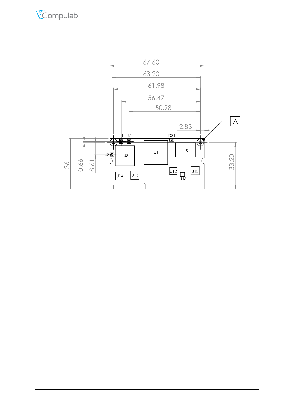
Carrier board Interface
6.3 Mechanical Drawings
Figure 3 CM-T43 Top
Revised September 2017 CM-T43 Reference Guide 76
Page 77
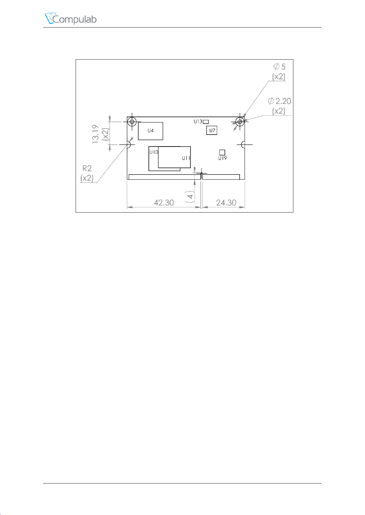
Carrier board Interface
Figure 4 CM-T43 bottom
1. All dimensions are in millimeters.
2. Height of all components is < 2mm.
3. Baseboard connectors provide 2mm board-to-board clearance.
4. Board thickness is 1.0mm.
Mechanical drawings are available in DXF format at
http://www.compulab.co.il/products/computer-on-modules/cm-t43/#devres
6.4 Standoffs/Spacers
CM-T43 has two mounting holes to physically secure the CoM/SoM to the carrier board. Secure
CM-T43 to the carrier board by mounting two spacers with any adequate screws and nuts. Spacers
must comply with the following specification:
M2x0.4 thread, 3.0±0.1 mm length
Revised September 2017 CM-T43 Reference Guide 77
Page 78
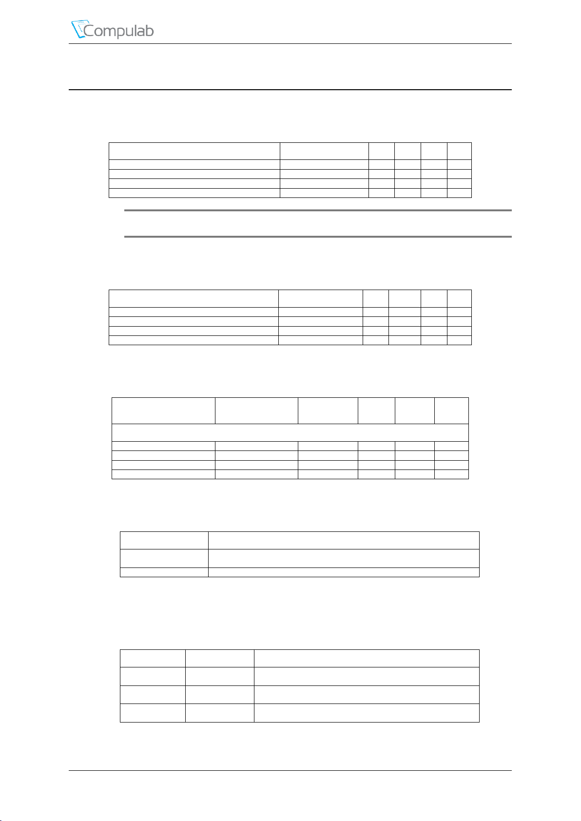
Operational Characteristics
Parameter
Condition
Min
Typ
Max
Unit
Main power supply voltage (VSYS)
With “WB” option
5.0 V Main power supply voltage (VSYS)
Without “WB” option
-0.3 5.8 V Backup battery supply voltage (VCC_RTC)
-0.3 3.6
V
VBUS inputs
-0.5 5.25
V
Parameter
Condition
Min
Typ
Max
Unit
Main power supply voltage (VSYS)
With “WB” option
3.3 5.0
V
Main power supply voltage (VSYS)
Without “WB” option
3.0 5.5 V Backup battery supply voltage (VCC_RTC)
2.2 3.3 V VBUS inputs
0.0
5.0
5.25
V
Parameter
Operating
Conditions
Min
Typ
Max
Unit
Multifunctional Digital I/O
VIH
2
V
VIL
0.8
V
VOH
IOH = 6mA
2.75
V
VOL
IOL = 6mA
0.45
V
Interface
ESD Performance
Multifunctional, USB &
ADC
±2kV Human Body Model (HBM), per ANSI/ESDA/JEDEC JS001
±0.5kV Charged Device Model (CDM) per JESD22-C101
Ethernet
±2kV Electrostatic discharge tolerance - Human Body Model
Range
Temp.
Description
Commercial
0o to 70o C
Sample boards from each batch are tested for the lower and upper
temperature limits. Individual boards are not tested.
Extended
-20o to 70o C
Every board undergoes a short test for the lower limit (-20o C)
qualification.
Industrial
-40o to 85o C
Every board is extensively tested for both lower and upper limits
and at several midpoints.
7 OPERATIONAL CHARACTERISTICS
7.1 Absolute Maximum Ratings
Table 70 Absolute Maximum ratings
NOTE: Exceeding the absolute maximum ratings may damage the device.
7.2 Recommended Operating Conditions
Table 71 Recommended Operating Conditions
7.3 DC Electrical Characteristics
Table 72 DC Electrical Characteristics
7.4 ESD Performance
Table 73 ESD Performance
7.5 Operating Temperature Ranges
The CM-T43 is available with three options of operating temperature range.
Table 74 CM-T43 Temperature Range Options
Revised September 2017 CM-T43 Reference Guide 78
Page 79
Application Notes
8 APPLICATION NOTES
8.1 Carrier Board Design Guidelines
Ensure that all VSYS and GND power pins are connected.
Major power rails - VSYS and GND must be implemented by planes, rather than traces.
Using at least two planes is essential to ensure the system signal quality, because the
planes provide a current return path for all interface signals.
It is recommended to put several 100nF and 10/100uF capacitors between VSYS and
GND near the mating connectors.
It is recommended to connect the standoff holes of the carrier board to GND, in order to
improve EMC.
Except for a power connection, no other connection is mandatory for CM-T43 operation.
All power-up circuitry and all required pullups/pulldowns are available onboard CM-T43.
If for some reason you decide to place an external pullup or pulldown resistor on a certain
signal (for example - on the GPIOs), first check the documentation of that signal provided
in this manual. Certain signals have on-board pullup/pulldown resistors required for
proper initialization. Overriding their values by external components will disable board
operation.
You must be familiar with signal interconnection design rules. There are many sensitive
groups of signals. For example:
Ethernet, SATA, USB and more signals must be routed in differential pairs and by a
controlled impedance trace.
Audio input must be decoupled from possible sources of carrier board noise.
Be careful when placing components under the CM-T43 module. The carrier board
interface connector provides 1mm mating height. Bear in mind that there are components
on the underside of the CM-T43.
Refer to the SB-SOM-T43 carrier board reference design schematics.
8.2 Carrier Board Troubleshooting
Using grease solvent and a soft brush, clean the contacts of the mating connectors of both
the module and the carrier board. Remnants of soldering paste can prevent proper contact.
Take care to let the connectors and the module dry entirely before re-applying power –
otherwise corrosion may occur.
Using an oscilloscope, check the voltage levels and quality of the VSYS power supply. It
should be as specified in section 7.2. Check that there is no excessive ripple or glitches.
First perform the measurements without plugging in the module. Then plug in the module
and measure again. Measurement should be performed on the pins of the mating
connector.
Using an oscilloscope, verify that the GND pins of the mating connector are indeed at
zero voltage level and that there is no ground bouncing. The module must be plugged in
during the test.
Create a "minimum system" - only power, mating connectors, the module and a serial
interface.
Check if the system starts properly. In system larger than the minimum, possible sources
of disturbance could be:
Devices improperly driving the local bus
External pullup/pulldown resistors overriding the module on-board values, or any other
component creating the same "overriding" effect
Faulty power supply
Revised September 2017 CM-T43 Reference Guide 79
Page 80
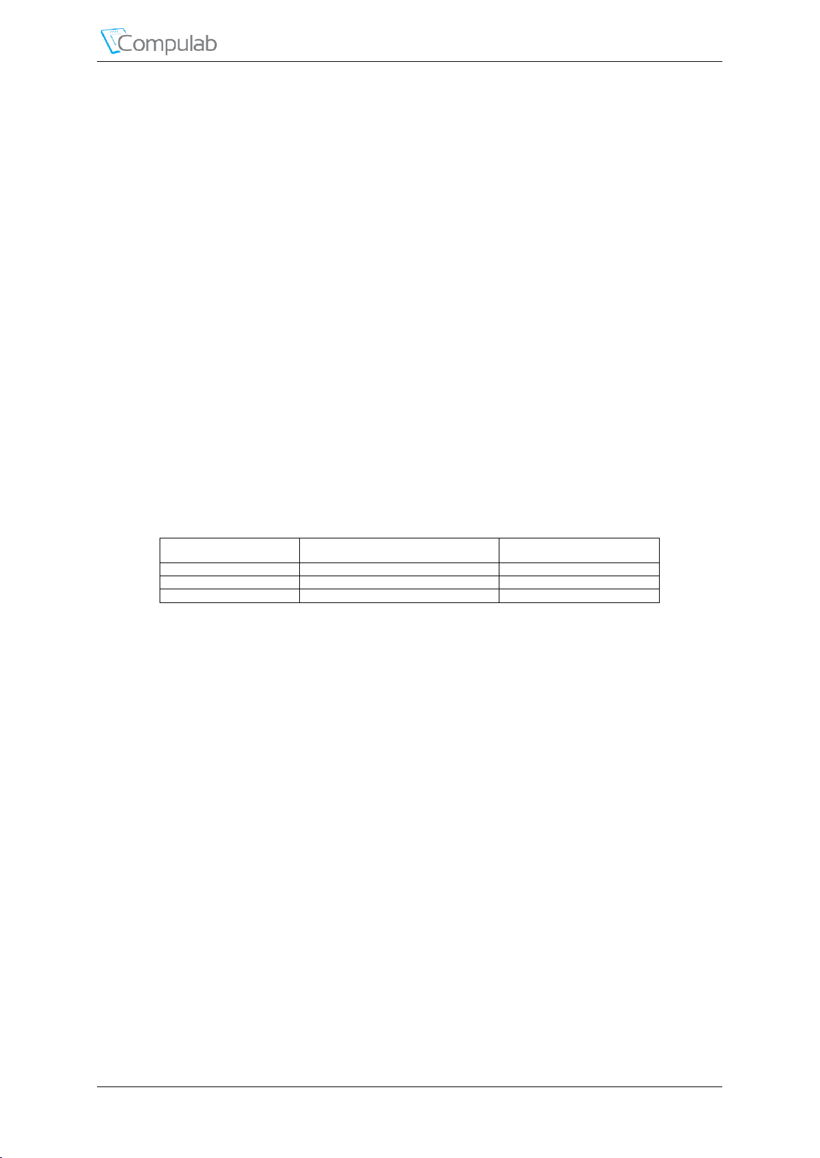
Application Notes
Vendor
P/N
Package
UDE
RB1-125BAK1A
Integrated RJ45
UNE
U50{79}G8-09-B122-B12-BT
Integrated, Dual RJ45
YDS
45F-10202GDD2
Integrated, Dual USB + RJ45
In order to avoid possible sources of disturbance, it is strongly recommended to start with
a minimal system and then to add/activate off-board devices one by one.
Check for the existence of soldering shorts between pins of mating connectors. Even if the
signals are not used on the carrier board, shorting them on the connectors can disable the
module operation. An initial check can be performed using a microscope. However, if
microscope inspection finds nothing, it is advisable to check using an X-ray, because
often solder bridges are deep beneath the connector body. Note that solder shorts are the
most probable factor to prevent a module from booting.
Check possible signal short circuits due to errors in carrier board PCB design or assembly.
Improper functioning of a customer carrier board can accidentally delete boot-up code
from CM-T43, or even damage the module hardware permanently. Before every new
attempt of activation, check that your module is still functional with CompuLab SB-SOMT43 carrier board.
It is recommended to assemble more than one carrier board for prototyping, in order to
ease resolution of problems related to specific board assembly.
8.3 Ethernet Magnetics Implementation
8.3.1 Magnetics Selection
Refer to the table below for compatible magnetics. The list of “Qualified Magnetics” contains
magnetics verified for proper functional operation by CompuLab. Designers should test and
qualify all magnetics before using them in an application.
Table 75 Qualified Magnetics
8.3.2 Magnetics Connection
For magnetic modules connection, please refer to the SB-SOM-T43 reference design schematics
Revised September 2017 CM-T43 Reference Guide 80
 Loading...