

Page 1

CL-SOM-AM57x
Reference Guide
Page 2
Legal
© 2016 Compulab Ltd.
All Rights Reserved. No part of this document may be photocopied, reproduced, stored in a
retrieval system, or transmitted, in any form or by any means whether, electronic, mechanical, or
otherwise without the prior written permission of Compulab Ltd.
No warranty of accuracy is given concerning the contents of the information contained in this
publication. To the extent permitted by law no liability (including liability to any person by
reason of negligence) will be accepted by Compulab Ltd., its subsidiaries or employees for any
direct or indirect loss or damage caused by omissions from or inaccuracies in this document.
Compulab Ltd. reserves the right to change details in this publication without notice.
Product and company names herein may be the trademarks of their respective owners.
Compulab Ltd.
P.O. Box 687 Yokneam Illit
20692 ISRAEL
Tel: +972 (4) 8290100
http://www.compulab.com
Fax: +972 (4) 8325251
Revised April 2018 CL-SOM-AM57x 2
Page 3
Table of Contents
Table of Contents
1 INTRODUCTION .......................................................................................................... 6
1.1 About This Document .................................................................................................. 6
1.2 CL-SOM-AM57x Part Number Legend ...................................................................... 6
1.3 Related Documents ...................................................................................................... 6
2 OVERVIEW ................................................................................................................... 7
2.1 Highlights .................................................................................................................... 7
2.2 Block Diagram ............................................................................................................. 8
2.3 CL-SOM-AM57x Features .......................................................................................... 9
3 CORE SYSTEM COMPONENTS ............................................................................. 11
3.1 AM57x SoC ............................................................................................................... 11
3.1.3 Display Subsystem ........................................................................................... 12
3.2 Memory ...................................................................................................................... 14
3.2.1 DRAM .............................................................................................................. 14
3.2.2 Bootloader Storage ........................................................................................... 14
3.2.3 General Purpose Storage .................................................................................. 14
4 PERIPHERAL INTERFACES ................................................................................... 15
4.1 Display Interface ........................................................................................................ 17
4.1.1 Parallel Display interface .................................................................................. 17
4.1.2 HDMI Interface ................................................................................................ 18
4.1.3 LVDS Display interface ................................................................................... 18
4.2 Parallel Camera Interface .......................................................................................... 19
4.3 PCI Express ............................................................................................................... 26
4.4 SATA ......................................................................................................................... 27
4.5 USB 3.0...................................................................................................................... 27
4.6 USB2.0 ports.............................................................................................................. 28
4.7 Ethernet ...................................................................................................................... 29
4.8 Wireless Interfaces ..................................................................................................... 30
4.8.1 WLAN Only ..................................................................................................... 30
4.8.2 Dual Band WLAN & Bluetooth ....................................................................... 31
4.9 Analog Audio ............................................................................................................. 31
4.10 Digital Audio (McASP) ........................................................................................ 33
4.11 MMC / SD /SDIO ................................................................................................. 34
4.12 UART .................................................................................................................... 35
4.13 SPI ......................................................................................................................... 38
4.14 I2C ......................................................................................................................... 39
4.15 CAN Bus ............................................................................................................... 39
4.16 Resistive Touch Interface ...................................................................................... 40
4.17 HDQ / 1-Wire........................................................................................................ 40
4.18 Enhanced High Resolution PWM module (eHRPWM) ....................................... 41
4.19 Enhanced Capture module (eCAP) ....................................................................... 41
Revised April 2018 CL-SOM-AM57x 3
Page 4
Table of Contents
4.20 Quadrature Encoder Pulse module (eQEP) ........................................................... 42
4.21 PRU-ICSS ............................................................................................................. 42
4.21.1 PRU-ICSS MII ................................................................................................. 42
4.21.2 PRU-ICSS UART ............................................................................................. 43
4.21.3 PRU-ICSS Industrial Ethernet Peripheral ........................................................ 43
4.21.4 PRU-ICSS Enhanced Capture Event Module (PRU-ICSS eCAP) ................... 44
4.21.5 PRU-ICSS GPI / GPO ...................................................................................... 44
4.22 General Purpose Timer ......................................................................................... 46
4.23 GPIO ..................................................................................................................... 47
5 SYSTEM LOGIC ......................................................................................................... 50
5.1 Power Supply ............................................................................................................. 50
5.2 System and Miscellaneous Signals ............................................................................ 50
5.2.1 Power Management .......................................................................................... 50
5.2.2 General Purpose clocks .................................................................................... 50
5.2.3 Flash Write-protection ...................................................................................... 51
5.3 Reset .......................................................................................................................... 51
5.4 Boot Sequence ........................................................................................................... 51
5.5 Signal Multiplexing Characteristics .......................................................................... 53
5.6 RTC ............................................................................................................................ 63
5.7 LED ............................................................................................................................ 63
6 CARRIER BOARD INTERFACE ............................................................................. 64
6.1 Connector Pinout ....................................................................................................... 64
6.2 Mechanical Drawings ................................................................................................ 74
6.3 Heat Spreader and Cooling Solutions ........................................................................ 75
6.4 Standoffs/Spacers ...................................................................................................... 75
7 OPERATIONAL CHARACTERISTICS .................................................................. 76
7.1 Absolute Maximum Ratings ...................................................................................... 76
7.2 Recommended Operating Conditions ........................................................................ 76
7.3 DC Electrical Characteristics ..................................................................................... 76
7.4 ESD Performance ...................................................................................................... 76
7.5 Operating Temperature Ranges ................................................................................. 77
8 APPLICATION NOTES ............................................................................................. 78
8.1 Carrier Board Design Guidelines ............................................................................... 78
8.2 Carrier Board Troubleshooting .................................................................................. 78
8.3 Ethernet Magnetics Implementation .......................................................................... 79
8.3.1 Magnetics Selection .......................................................................................... 79
8.3.2 Magnetics Connection ...................................................................................... 79
Revised April 2018 CL-SOM-AM57x 4
Page 5
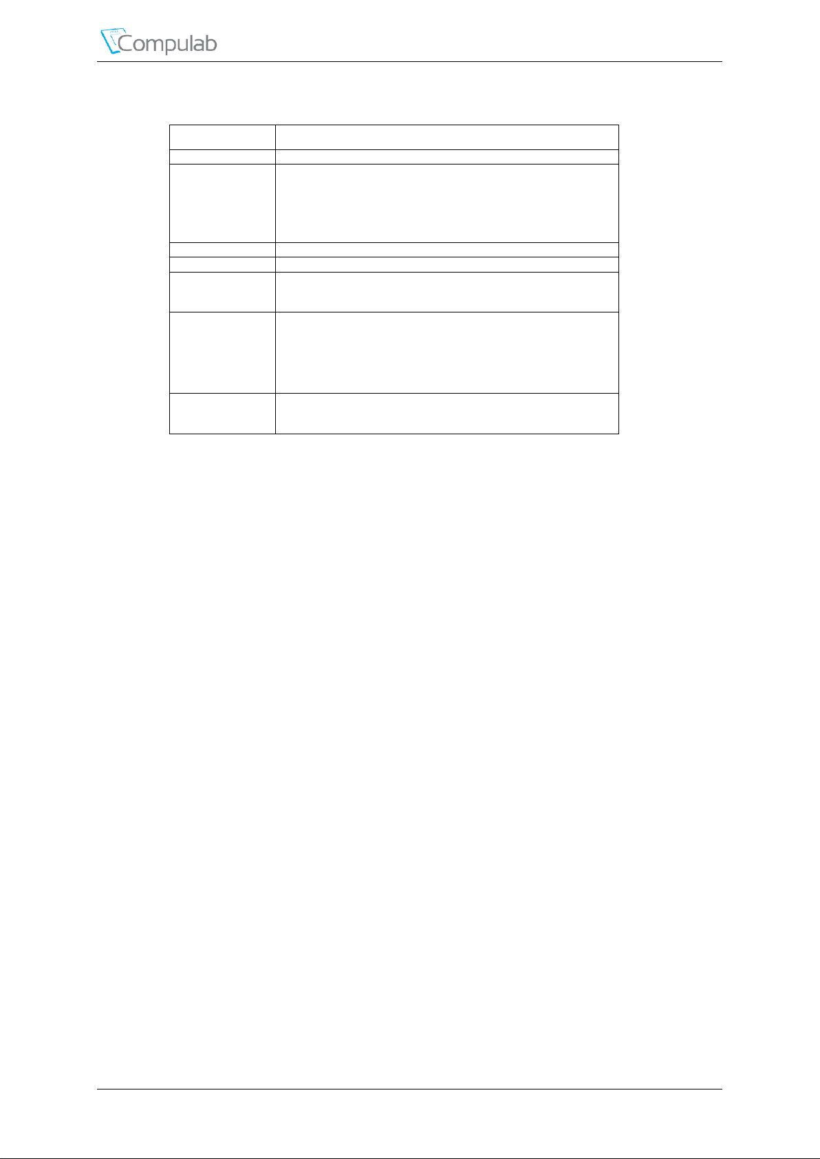
Revision Notes
Date
Description
Nov 2015
First release
Dec 2016
(4) Added full description of all available AM5718x SoC pins on main
CL-SOM-AM57x SO-DIMM connector.
(4.1.1) Added description for all availability options for Parallel
Display interface.
(5.5) Signal Multiplexing table: embedded excel files updated, one
general table for AM5728 and AM5718 SOC added to this doc.
Aug 2017
(4.8) Updated features list
Oct 2017
(4.1.3) Updated note details
Jan 2018
(4.5) Updated USB 3.0 Interface Signals table
(4.12) Updated availability limitation on SO-DIMM pins 147, 149,
151, and 157 in table 38 (UART9) and table 39 (UART10).
Mar 2018
(4.14) Updated I2C2 Interface Signals
(6.1) Updated I2C2 on SO-DIMM pin 25 and 31
Updated I2C2 on pins 25 and 31 in attached excel file
(4.12) Table 37 Updated UART8 on Pin# 11
(6.1) Table 68, pins 11 updated
Updated UART8 on pin 11 in attached excel file
Apr 2018
(4.8.2) Updated description of UART used for Bluetooth when
WL1837MOD is populated
(4.12) Table 39 updated Description and Availability
Table 1 Revision Notes
Please check for a newer revision of this manual at the CompuLab web site
http://www.compulab.com. Compare the revision notes of the updated manual from the web site
with those of the printed or electronic version you have.
Revised April 2018 CL-SOM-AM57x 5
Page 6
Introduction
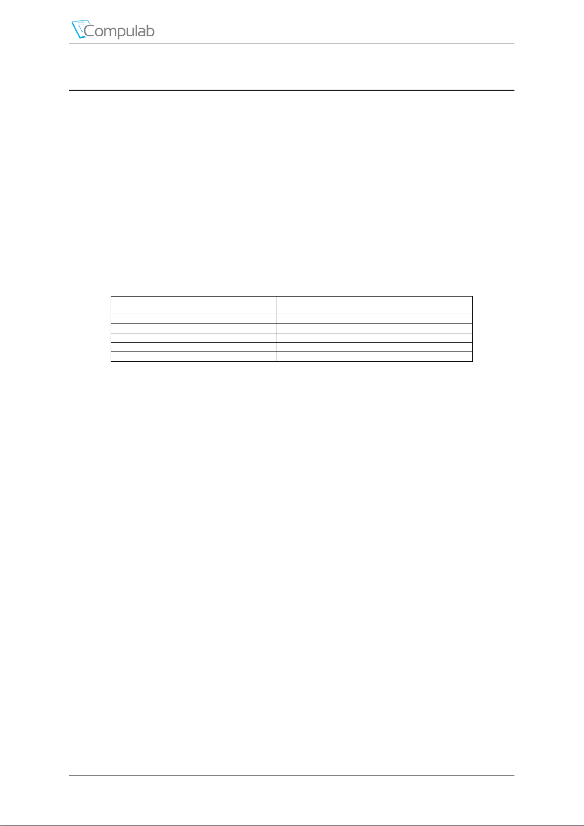
Document
Location
CL-SOM-AM57x Developer Resources
http://www.compulab.com/
AM57x Reference Manual
AM57x Reference Manual
AM57x Datasheet
http://www.ti.com
1 INTRODUCTION
1.1 About This Document
This document is part of a set of reference documents providing information necessary to operate
and program CompuLab CL-SOM-AM57x Computer-on-Module.
1.2 CL-SOM-AM57x Part Number Legend
Please refer to the CompuLab website ‘Ordering information’ section to decode the CL-SOMAM57x part number: http://www.compulab.com/products/computer-on-modules/cl-som-am57xti-am5728-am5718-system-on-module/#ordering.
1.3 Related Documents
For additional information, refer to the documents listed in Table 2.
Table 2 Related Documents
Revised April 2018 CL-SOM-AM57x 6
Page 7
Overview
2 OVERVIEW
2.1 Highlights
Texas Instruments Sitara AM57x processors, 1.5GHz
Up to 4GB DDR3 and 32GB on-board eMMC
PowerVR SGX544 GPU, 1080p VPU and C66x DSP
Dual-band 802.11a/b/g/n WiFi and Bluetooth 4.1 BLE
2x PCIe, 2x GbE, SATA, USB3, 3x USB2, 9x UART, 87x GPIO
Miniature size: 60 x 68 x 5 mm
CL-SOM-AM57x is a miniature System-on-Module / Computer-on-Module designed as a
building block for integration into embedded applications. CL-SOM-AM57x is built around the
Texas Instruments Sitara AM57x ARM Cortex-A15 System-on-Chip family. The SoC is
supplemented with up-to 4GB DDR3 and 32GB of on-board eMMC storage.
Featuring an unprecedented set of dedicated graphics acceleration and video processing engines,
CL-SOM-AM57x delivers high-performance multimedia and image processing capabilities. Dual
C66x DSP cores and dedicated dual-core ARM Cortex-M4 IPUs make CL-SOM-AM57x a
powerful platform for image and video processing systems, while dual PowerVR SGX544 GPU
and IVA-HD video sub-system enable multimedia demanding applications.
Delivering a wide range of embedded interfaces and a PRU-ICSS coprocessor dedicated for realtime processing and industrial protocols, CL-SOM-AM57x is an ideal selection for industrial
automation and control systems. Dual Gbit Ethernet, 2x2 MIMO dual-band 802.11a/b/g/n WiFi
and Bluetooth 4.1 make CL-SOM-AM57x an excellent solution for networking, communications
and IoT applications.
CL-SOM-AM57x is provided with comprehensive documentation and full ready-to-run SW
packages for the Linux operating system.
Revised April 2018 CL-SOM-AM57x 7
Page 8
Overview
IVA HD
1080p Video
DSP
2x C66x
2x ARM
Cortex A15
2x
PRU-ICSS
IPU1
2x Cortex-M4
Integrated
Ethernet
switch
DDR3
Ctrl1
DDR3
Ctrl2
1x JTAG
SmartReflex
DDR3
Up to 2GB
DDR3
Up to 2GB
Test points
SPI Flash
(primary
bootloader
storage)
PMIC
TPS6590375
I2C EEPROM
(board info)
32 bit
32 bit
JTAG
QSPI CS0
24/8bit Video
Input Port
16bit Video
Input Port
Parallel 24bit
display
2x Ethernet Ports
(1Gbps)
I2C
1-WIRE
SPI
UART
QSPI
McASP
CAN
GPIO
eCAP
eHRPWM
eQEP
PRU UART
PRU eCAP
PRU MII
PRU Industrial
Ethernet
EGPI
EGP0
M
ultifunctional signals (m
uxed)
204-pin SODIMM edge connector
up to 3x I2C bus
up to 1x HDQ 1-wire
up to 9x UART
up to 3x SPI
up to 3x eMMC/SD/SDIO
up to 4x I2S/McASP
up to 2x CAN bus
up to 87x GPIOs
up to 5x PWM (eHRPWM)
up to 8x Timer/PWM
up to 2x Capture Interface (eCAP)
up to 1x Quadrature Encoder
up to 2x PRU UART
up to 2x PRU eCAP
up to 1x PRU MII
up to 1x PRU Industrial Ethernet
up to 28x PRU EGPI
up to 32x PRU EGPO
up to 3x Video Input ports
GPMC
MMC2
UART10
MMC4
Optional bypass
(4 bit SDIO)
WLAN+BT
TI WiLink 8
Touch screen
contoller
LVDS 24 bit
Transmitter
USB 2.0
hub
Audio Codec
WM8731
S
tereo
Stereo
M
icrophone
McASP3
1x HDMI
1x USB 3.0
1x USB 2.0
2x PCIe
resistive
touch
QSPI CS1
LCD3 24 bit LVDS
Parallel RGB 24bit
USB 3.0
HDMI 1.4a
USB 2.0
USB 2.0
USB 2.0
USB 2.0
PCIe x1
PCIe x1
SATA-II
1x SATA
I2C1
I2C4
Texas
Instruments
AM57x
eMMC/SD/SDIO
Optional bypass
1Gbit PHY
RGMII0
1Gbit PHY
RGMII1 1Gbit Eth
1Gbit Eth
RTC
SLC NAND
(512MB - 1GB)
or
eMMC
(4GB - 32GB)
Optional bypass
GPU
2x SGX544
IPU2
2x Cortex-M4
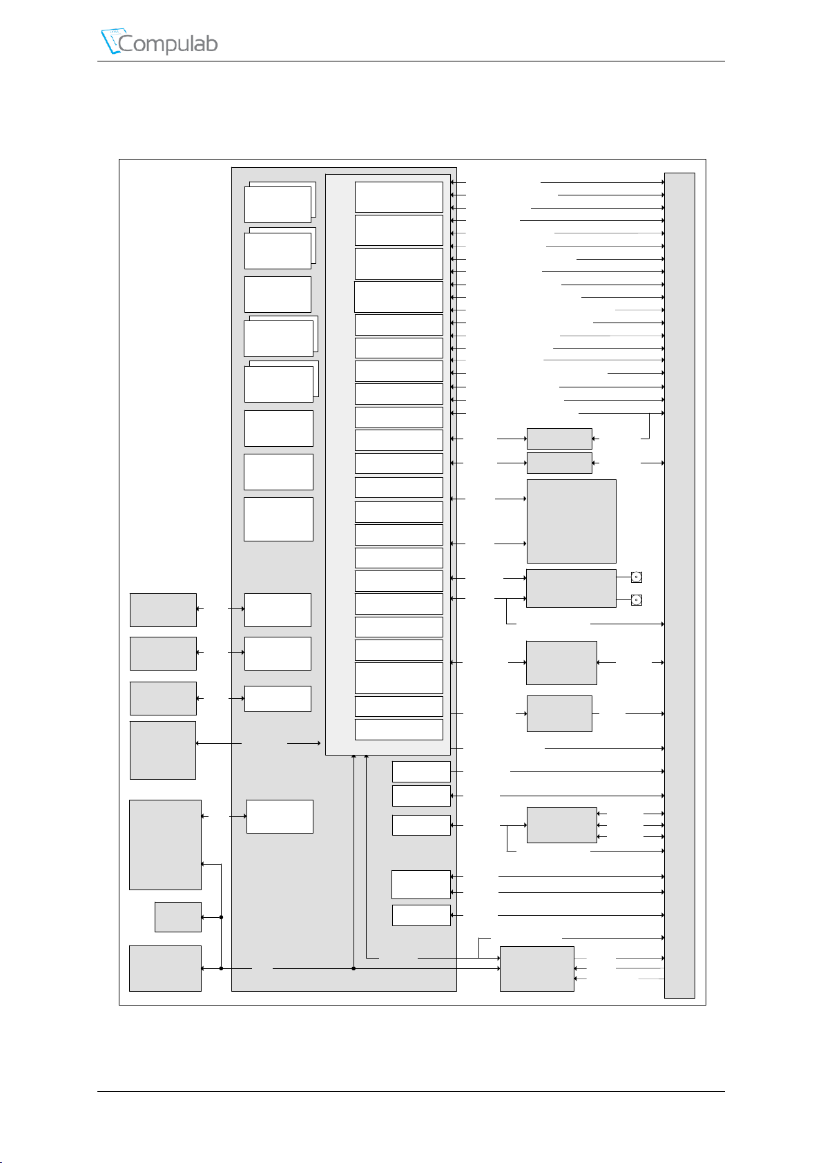
2.2 Block Diagram
Figure 1 CL-SOM-AM57x Block Diagram
Revised April 2018 CL-SOM-AM57x 8
Page 9
Overview
Feature
Description
Option
CPU Core and Graphics
CPU
Texas Instruments Sitara AM5728 dual-core ARM Cortex-A15, 1.5GHz
NEON SIMD and VFPv4
C1500D
Texas Instruments Sitara AM5718 single-core ARM Cortex-A15, 1.5GHz.
NEON SIMD and VFPv4
C1500
DSP
Up to 2x TMS320C66x DSP cores
C1500x
GPU
Up to 2x PowerVR SGX544 3D GPU cores
C1500x
Vivante GC320 2D GPU
+
Video
IVA-HD video sub-system supporting 1080p HD decoding / encoding
+
Image
Processing
2x dual-core ARM Cortex-M4 IPU, 213MHz
+
Real-Time
Coprocessor
2x PRU-ICSS supporting EtherCAT, PROFIBUS, PROFINET,
EtherNet/IP and Powerlink protocols
+
Memory and Storage
RAM
512MB – 4GB, DDR3-1333, single / dual channel 32-bit data bus
D
Storage
On-board SLC NAND flash, 512MB – 1GB
N
On-board eMMC flash, 4GB - 32GB
Display and Camera
Display
Parallel RGB, 24-bit, up to 1920 x 1200
+
HDMI 1.4a, up to 1920 x 1200
+
LVDS, up to 1920 x 1080
L
Touchscreen
On-board 4-wire resistive touch-screen controller
I
Capacitive touch-screen support through SPI and I2C interfaces
+
Camera
Up to 3x parallel camera interfaces
+
Network
Gigabit Ethernet
Up to 2x 10/100/1000Mbps Ethernet ports (MAC+PHY)
E1/E2
WiFi
802.11b/g/n WiFi interface
TI WiLink 8 WL1801 chipset
W
Dual-band 2x2 802.11a/b/g/n WiFi interface
TI WiLink 8 WL1837 chipset
WAB
Bluetooth
Bluetooth 4.1 BLE
WAB
Audio
Analog Audio
Audio codec with stereo output, stereo input and microphone support
A
Digital Audio
Up to 4x I2S digital audio interfaces
+
HDMI audio output
+
I/O
PCI Express
2x PCIe x1 Gen. 2
+
SATA
SATA-II, 3Gbps
+
USB
1x USB3.0 dual-role + 1x USB2.0 host
U2
1x USB3.0 dual-role + 3x USB2.0 host
U4
Serial Ports (UARTs)
Up to 9x UART ports, 16C750 compatible, up to 12 Mbps
+
CAN bus
Up to 2x CAN bus
+
MMC/SD/SDIO
Up to 3x MMC/SD/SDIO interfaces
+
SPI
Up to 3x SPI bus interfaces
+
I2C
Up to 3x I2C interfaces
+
1-Wire
1-Wire interface
+
Timer/PWM
Up to 8x Timer/PWM outputs
+
GPIO
Up to 87x GPIO signals (shared with other functions)
+
System Logic
RTC
Real time clock, powered by external lithium battery
+
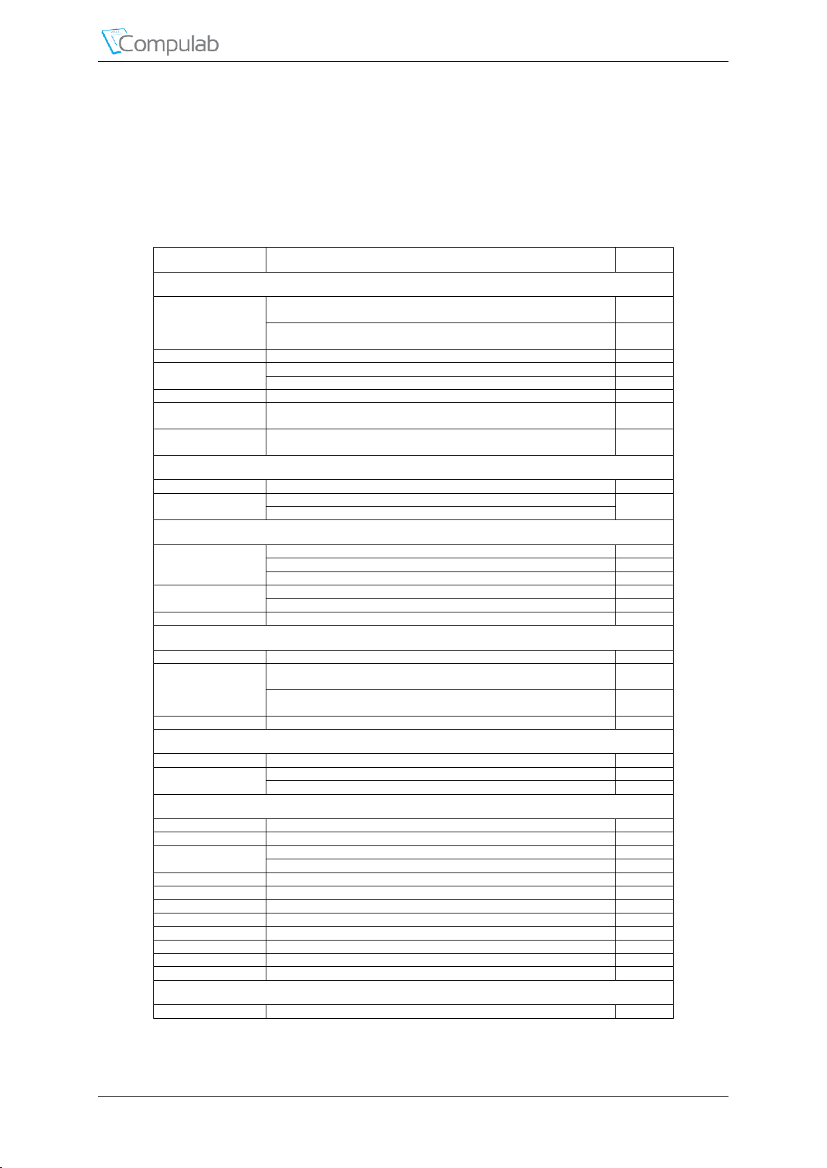
2.3 CL-SOM-AM57x Features
The "Option" column specifies the CoM/SoM configuration option required to have the particular
feature. When a CoM/SoM configuration option is prefixed by “NOT”, the particular feature is
only available when the option is not used. A feature is only available when a CoM/SoM
configuration complies with all options denoted in the “Option” column.
"+" means that the feature is always available.
Table 3 Features and Configuration options
Revised April 2018 CL-SOM-AM57x 9
Page 10
Overview
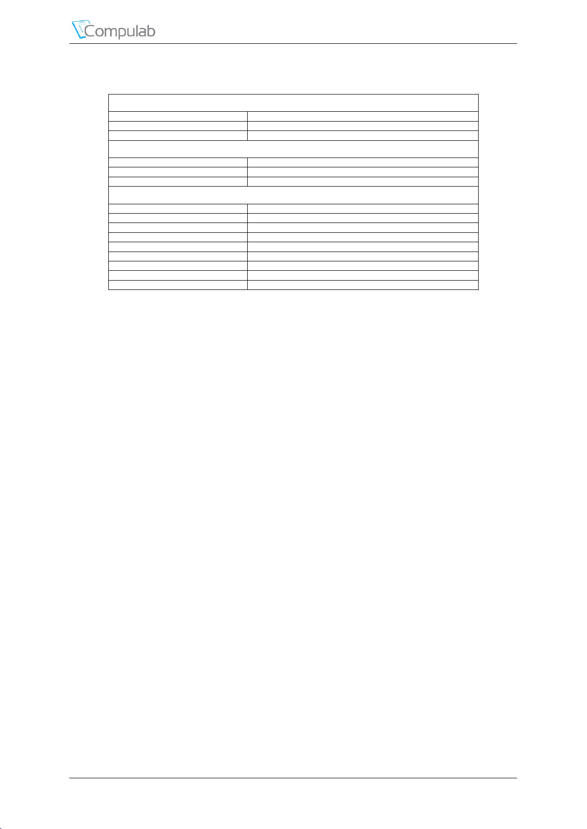
Electrical Specifications
Supply Voltage
4.2V to 5V
Digital I/O voltage
3.3V
Active power consumption
2.5 – 6.5 W, depending on board configuration and system workload
Mechanical Specifications
Dimensions
60 x 68 x 5 mm
Weight
35 gram
Connectors
204-pin SO-DIMM edge connector
Environmental and Reliability
MTTF
> 200,000 hours
Operation temperature (case)
Commercial: 0° to 70° C
Extended: -20° to 70° C
Industrial: -40° to 85° C
Storage temperature
-40° to 85° C
Relative humidity
10% to 90% (operation)
05% to 95% (storage)
Shock
50G / 20 ms
Vibration
20G / 0 - 600 Hz
Table 4 Electrical, Mechanical and Environmental Specifications
Revised April 2018 CL-SOM-AM57x 10
Page 11
Core system components
3 CORE SYSTEM COMPONENTS
3.1 AM57x SoC
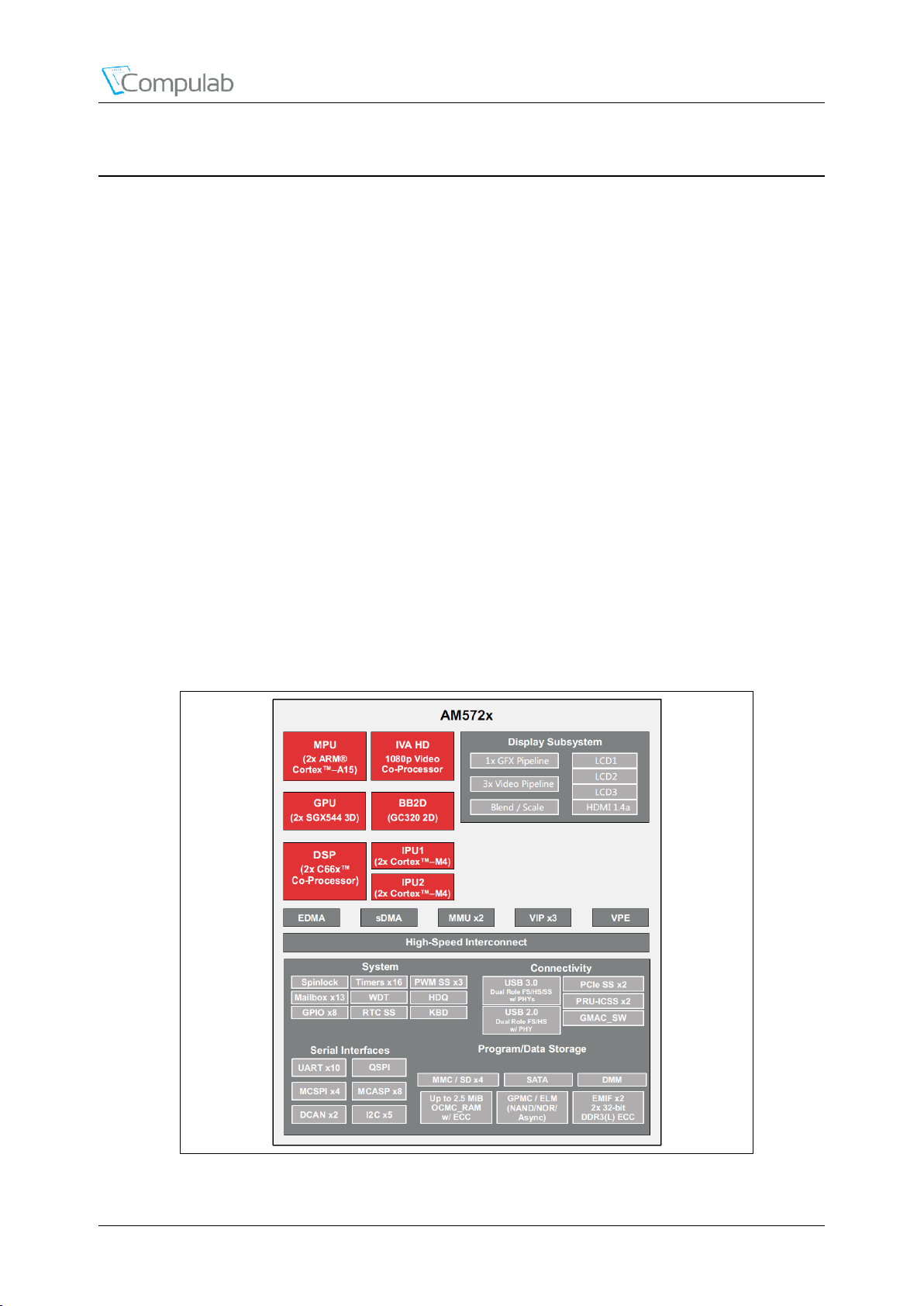
The TI Sitara AM57x system-on-chip (SoC) is built around dual-core ARM Cortex-A15 CPU. Dual
C66x VLIW DSP cores and dedicated ARM Cortex-M4 IPUs make AM572x a powerful platform for
image and video processing systems, while dual PowerVR SGX544 GPU and IVA-HD video subsystem enable multimedia demanding applications.
Up to 1500-MHz Sitara™ ARM® Single/Dual Cortex®-A15 32-Bit RISC processor
NEON™ SIMD Coprocessor and Vector Floating Point (VFPv4) per CPU
32-KiB instruction and 32-KiB data level 1 (L1) cache per CPU
Shared 1-MiB/2-MiB level 2 (L2) cache
On-Chip 512KiB/2.5MiB Shared Memory (RAM)
48-KiB bootable ROM
Up to 2 C66x™ Floating-Point VLIW DSP
Image and video accelerator high-definition (IVA-HD) subsystem
Two ARM® Dual Cortex®-M4 Image Processing Units (IPUs)
Single/Dual-Core PowerVR® SGX544™ 3D GPU
2D-Graphics Accelerator (BB2D) Subsystem, including Vivante™ GC320 Core
Crypto Hardware Accelerators (AES, SHA, RNG, DES and 3DES)
Two dual-core Programmable Real-time Unit and Industrial Communication Subsystems
(PRUICSS)
Figure 2 AM572x Block Diagram
Revised April 2018 CL-SOM-AM57x 11
Page 12
Core system components
3.1.1 DSP Subsystem
The AM57x SoC includes up to two identical instances (DSP1 and DSP2) of a digital signal
processor (DSP), based on the TI's standard TMS320C66x™ DSP CorePac core.
Each of the two DSP subsystems integrated in the device includes the following components:
A TMS320C66x™ CorePac DSP core
Dedicated enhanced data memory access engine – EDMA
A level 2 (L2) interconnect network (DSP NoC)
Two memory management units (on EDMA L2 interconnect and DSP MDMA paths)
Dedicated system control logic (DSP_SYSTEM)
3.1.2 Dual Cortex-M4 IPU Subsystem
The AM57x SoC instantiates two dual Cortex™-M4 image processor unit (IPU) subsystems:
IPU1 subsystem is available for general purpose usage
IPU2 subsystem is dedicated to IVA support and is not available for other processing
Each IPU subsystem integrates the following:
Two ARM Cortex-M4 microprocessors
ARMv7-M and Thumb®-2 instruction set architecture (ISA)
ARMv6 SIMD and digital signal processor (DSP) extensions
Single-cycle MAC
Integrated nested vector interrupt controller (NVIC)
Integrated bus matrix
Unicache interface
Level 2 (L2) master interface (MIF) splitter
On-chip ROM and banked RAM memory
3.1.3 Display Subsystem
The AM57x display subsystem provides the control signals required to interface the device system
memory frame buffer (SDRAM) directly to the displays. It supports hardware cursor, independent
gamma curve on all interfaces, multiple-buffer, and programmable color phase rotation.
3.1.4 3D Graphics Accelerator
The AM57x 3D graphics processing unit (GPU) accelerates 2-dimensional (2D) and 3-dimensional
(3D) graphics and compute applications. It is based on the POWERVR® SGX544 core from
Imagination Technologies which includes the following key features:
2D and 3D graphics
API support for industry standards: OpenGL® - ES 1.1 and 2.0
Multicore GPU architecture (with SGX544-MP2 core)
Tile-based deferred rendering architecture
Universal Scalable Shader Engine (USSE™)
Present and texture load accelerator (PTLA)
Revised April 2018 CL-SOM-AM57x 12
Page 13
Core system components
3.1.5 2D Graphics Accelerator
The 2D graphics accelerator subsystem accelerates 2D graphics applications. The 2D graphics
accelerator subsystem is based on the GC320 2D GPU core from Vivante Corporation. The hardware
acceleration is brought to numerous 2D applications, including on-screen display and touch screen
user interfaces, graphical user interfaces (GUIs) and menu displays, flash animation, and gaming. The
GC320 2D Main Features include the following:
API support:
OpenWF™, DirectFB
GDI/DirectDraw™
BB2D architecture
Hardware acceleration for DirectFB
3.1.6 PRU-ICSS
There are two Programmable Real-time Unit and Industrial Communication Subsystems (PRU-ICSS)
in the device. The PRU-ICSS enables additional peripheral interfaces and real-time protocols such as
EtherCAT, PROFINET, EtherNet/IP, PROFIBUS, Ethernet Powerlink, Sercos and others.
Each PRU-ICSS consists of dual 32-bit RISC cores (Programmable Real-Time Units, or PRUs),
shared data and instruction memories, internal peripheral modules, and an interrupt controller
(INTC). The programmable nature of the PRU cores, along with their access to pins, events and all
device resources, provides flexibility in implementing fast real-time responses, specialized data
handling operations, custom peripheral interfaces, and in offloading tasks from the other processor
cores of the device. The PRU-ICSS Key Features are:
Supports Protocols such as EtherCAT, PROFINET, EtherNet/IP, PROFIBUS, Ethernet
Powerlink, Sercos and more
Two Programmable Real-Time Units (PRUs) Subsystems With Two PRU Cores Each
Each Core is a 32-bit load/store RISC CPU core
12-KiB program RAM per PRU CPU
8-KiB data RAM per PRU CPU
Enhanced General-Purpose Inputs (EGPI) and Enhanced General-Purpose
Outputs (EGPO)
32-KiB general purpose memory RAM (signified RAM2) shared between PRU0 and PRU1
Peripherals Inside the PRU-ICSS:
One Ethernet MII_RT module
One MDIO Port
Industrial Ethernet Peripheral (IEP)
16550-compatible UART with a dedicated 192-MHz clock to support
Industrial Ethernet timer with 7/9 capture and 8 compare events
Enhanced Capture Module (ECAP)
Interrupt Controller
12-Mbps PROFIBUS
Revised April 2018 CL-SOM-AM57x 13
Page 14

Core system components
3.2 Memory
3.2.1 DRAM
AM5728 includes two 32-bit DDR controllers (EMIF1 and EMIF2). AM5718 includes one 32-bit
DDR controller (EMIF1).
CL-SOM-AM57x is equipped with up to 4GB of onboard DDR3 memory. The DDR3 data bus is 32bits wide and operates at 533 MHz clock frequency (DDR3-1066).
NOTE: 2GB and 4GB DDR3 memory capacities are available with C1500D option only.
3.2.2 Bootloader Storage
CL-SOM-AM57x is assembled with 2MBytes of SPI NOR flash. The SPI NOR flash is used for
boot-loader and configuration blocks storage.
3.2.3 General Purpose Storage
CL-SOM-AM57x is available with optional on-board storage designed to store the operating system
and user data. One of the following storage devices can be used as the main on-board storage:
eMMC flash (up to 32GB).
SLC NAND Flash (up to 1GB).
NOTE: SLC NAND and eMMC are mutually exclusive configuration options.
Revised April 2018 CL-SOM-AM57x 14
Page 15
Peripheral Interfaces
4 PERIPHERAL INTERFACES
CL-SOM-AM57x implements a variety of peripheral interfaces through the SODIMM-204 carrier
board connector. The following notes apply to interfaces available through the SODIMM-204
interface:
Some interfaces/signals are available only with/without certain configuration options of
CL-SOM-AM57x. The availability restrictions of each signal are described in the “Signals
description” table for each interface.
Many of the CL-SOM-AM57x carrier board interface pins are multifunctional. Up-to 16
functions (ALT modes) are accessible through each multifunctional pin. Multifunctional
pins are denoted with an asterisk (*). For additional details, please refer to chapter 5.5 of
this document.
Only one multifunctional pin can be used for each function, configuring several
multifunctional pins to implement the same function will result in unexpected system
behavior.
All of the CL-SOM-AM57x digital interfaces operate at 3.3V voltage levels, unless
otherwise noted.
The signals for each interface are described in the “Signal description” table for the interface in
question. The following notes provide information on the “Signal description” tables:
“Signal name” – The name of each signal with regards to the discussed interface. The
signal name corresponds to the relevant function in cases where the carrier board pin in
question is multifunctional.
“Pin#” – The carrier board interface pin number where the discussed signal is available,
multifunctional pins are denoted with an asterisk.
“Type” – Signal type, see the definition of different signal types below
“Description” – Signal description with regards to the interface in question.
“Availability” – Depending on CL-SOM-AM57x Configuration options, certain carrier
board interface pins are physically disconnected (floating) from the carrier board interface
connector on-board CL-SOM-AM57x. The “Availability” column summarizes
configuration requirements for each signal. All the listed requirements must be met (logical
AND) for a signal to be “available” unless otherwise noted.
Each described signal can be one of the following types. Signal type is noted in the “Signal
description” tables. Multifunctional pin direction, pull resistor and open drain functionality is
software controlled. The “Type” column header for multifunctional pins refers to the
recommended pin configuration with regards to the discussed signal.
“AI” – Analog Signal Input
“AO” – Analog Signal Output
“AIO” – Analog Signal Input/Output
“APO” – Analog Power Output
“API” – Analog Power Input
“I” – Digital Input
"O" – Digital Output
“IO” – Digital Input/Output
“IOD” – Open Drain Signal (not pulled up on-board CL-SOM-AM57x unless otherwise
noted).
"DS" – Differential Signaling
“PWR” – Power
“SPU” – Software controlled pull up to 3.3V
“SPD” – Software controlled pull down to GND
Revised April 2018 CL-SOM-AM57x 15
Page 16
Peripheral Interfaces
"PU18" – Always pulled up to 1.8V on-board CL-SOM-AM57x, (typ. 5KΩ-15KΩ).
"PU33" – Always pulled up to 3.3V on-board CL-SOM-AM57x, (typ. 5KΩ-15KΩ).
"PUSUPPLY" – Always pulled up to 3.8V - 5.25V on-board CL-SOM-AM57x, (typ.
5KΩ-15KΩ).
"PD" - Always pulled down on-board CL-SOM-AM57x, (typ. 5KΩ-15KΩ).
Revised April 2018 CL-SOM-AM57x 16
Page 17
Peripheral Interfaces
Signal Name
Pin
#
Type
Description
Availability
VOUT1_CLK
98* O Video Output 1 Clock output
Always
VOUT1_D0
106* O Video Output 1 Data output
Always
VOUT1_D1
108* O Video Output 1 Data output
Always
VOUT1_D10
128* O Video Output 1 Data output
Always
VOUT1_D11
130* O Video Output 1 Data output
Always
VOUT1_D12
134* O Video Output 1 Data output
Always
VOUT1_D13
136* O Video Output 1 Data output
Always
VOUT1_D14
138* O Video Output 1 Data output
Always
VOUT1_D15
140* O Video Output 1 Data output
Always
VOUT1_D16
94* O Video Output 1 Data output
Always
VOUT1_D17
92* O Video Output 1 Data output
Always
VOUT1_D18
142* O Video Output 1 Data output
Always
VOUT1_D19
144* O Video Output 1 Data output
Always
VOUT1_D2
110* O Video Output 1 Data output
Always
VOUT1_D20
146* O Video Output 1 Data output
Always
VOUT1_D21
148* O Video Output 1 Data output
Always
VOUT1_D22
74* O Video Output 1 Data output
Always
VOUT1_D23
76* O Video Output 1 Data output
Always
VOUT1_D3
112* O Video Output 1 Data output
Always
4.1 Display Interface
CL-SOM-AM57x display interface is derived from the AM57x display subsystem. The display
subsystem key features are:
Support of hardware cursor, independent gamma curve on all interfaces, multiple-buffer,
and programmable color phase rotation
Display controller:
Three video pipelines, one graphic pipeline, and one write-back pipeline
Three LCD outputs, each one with dedicated overlay manager, for support of
active matrix color displays (up to 24-bit interface)
One TV output with dedicated overlay manager to support HDMI v1.4a interface
(1080p @ 60 fps video and multichannel audio)
For additional details on display subsystem, please refer to the Sitara AM57x technical reference
manual.
4.1.1 Parallel Display interface
CL-SOM-AM57x display interface is derived from the AM57x display subsystem. The display
subsystem key features are:
Support of hardware cursor, independent gamma curve on all interfaces, multiple-buffer,
and programmable color phase rotation
Display controller:
Three video pipelines, one graphic pipeline, and one write-back pipeline
Three LCD outputs, each one with dedicated overlay manager, for support of
active matrix color displays (up to 24-bit interface)
One TV output with dedicated overlay manager to support HDMI v1.4a interface
(1080p @ 60 fps video and multichannel audio)
CL-SOM-AM57x provides access to the main LCD output (DPI1), referred in Sitara AM57x
technical reference manual as "VOUT1". The main features of VOUT1 interface are:
24-bit parallel CMOS output interface (DPI) (MIPI DPI 2.0, BT-656, or BT-1120)
Supporting up to WUXGA (1920 x 1200) with reduced blanking periods.
For additional details on display subsystem, please refer to the Sitara AM57x technical reference
manual. The table below summarizes the Parallel display interface signals
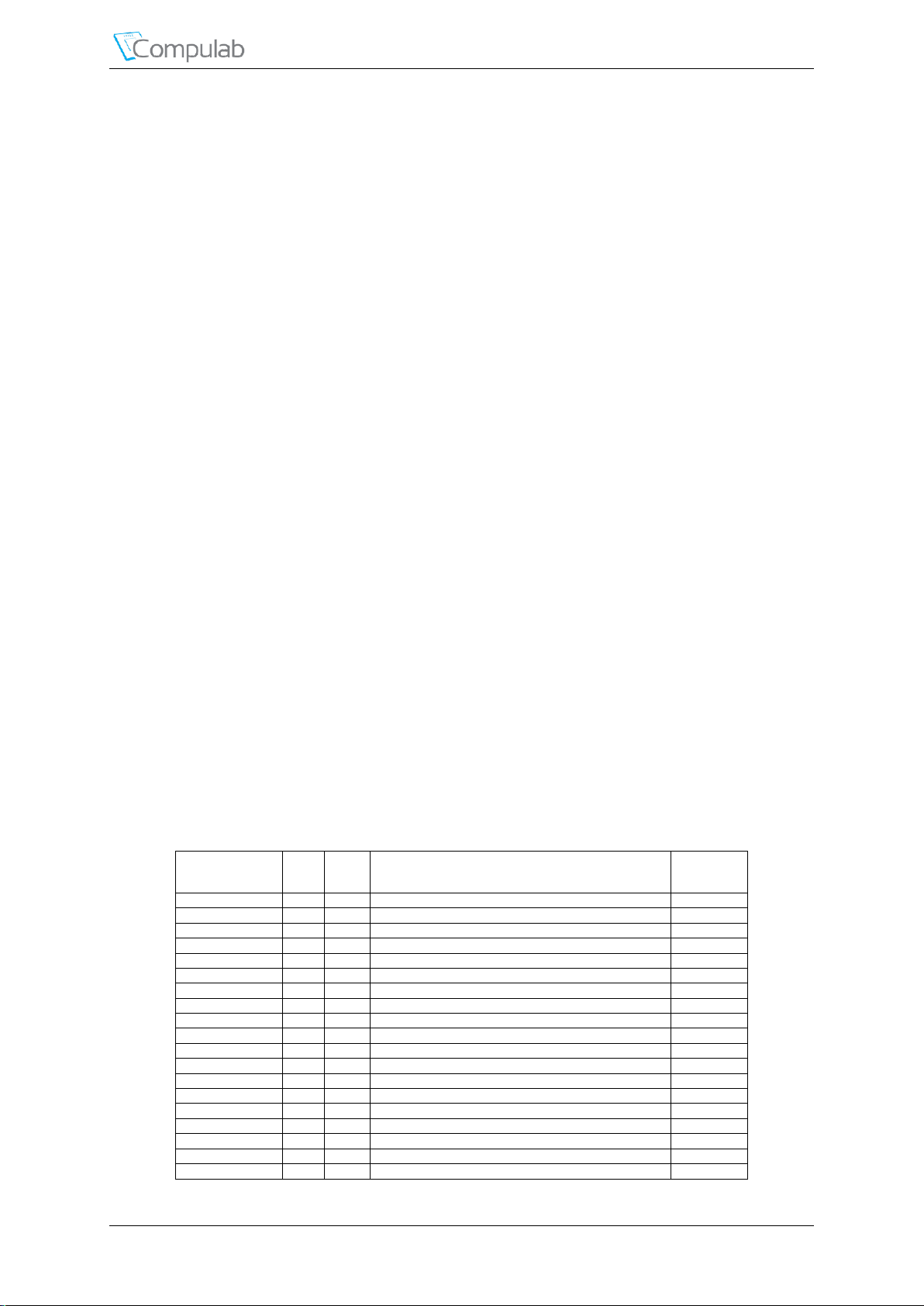
Table 5 Parallel display Interface Signals
Revised April 2018 CL-SOM-AM57x 17
Page 18
Peripheral Interfaces
Signal Name
Pin
#
Type
Description
Availability
VOUT1_D4
116* O Video Output 1 Data output
Always
VOUT1_D5
118* O Video Output 1 Data output
Always
VOUT1_D6
120* O Video Output 1 Data output
Always
VOUT1_D7
122* O Video Output 1 Data output
Always
VOUT1_D8
124* O Video Output 1 Data output
Always
VOUT1_D9
126* O Video Output 1 Data output
Always
VOUT1_DE
104* O Video Output 1 Data Enable output
Always
VOUT1_FLD
161*
O
Video Output 1 Field ID output. This signal is not used
for embedded sync modes.
Always
VOUT1_HSYNC
100*
O
Video Output 1 Horizontal Sync output.This signal is
not used for embedded sync modes.
Always
VOUT1_VSYNC
102*
O
Video Output 1 Vertical Sync output.This signal is not
used for embedded sync modes.
Always
Signal Name
Pin
#
Type
Description
Availability
HDMI1_CEC
34*
IOD
HDMI consumer electronic control
Always
HDMI1_CEC
56
IOD
HDMI consumer electronic control
With "C1500"
HDMI1_CLOCKX
30
ODS
HDMI clock differential positive or negative
Always
HDMI1_CLOCKY
32
ODS
HDMI clock differential positive or negative
Always
HDMI1_DATA0X
36
ODS
HDMI data 0 differential positive or negative
Always
HDMI1_DATA0Y
38
ODS
HDMI data 0 differential positive or negative
Always
HDMI1_DATA1X
42
ODS
HDMI data 1 differential positive or negative
Always
HDMI1_DATA1Y
44
ODS
HDMI data 1 differential positive or negative
Always
HDMI1_DATA2X
48
ODS
HDMI data 2 differential positive or negative
Always
HDMI1_DATA2Y
50
ODS
HDMI data 2 differential positive or negative
Always
HDMI1_DDC_SCL
25*
IOD
HDMI display data channel clock
Always
HDMI1_DDC_SDA
31*
IOD
HDMI display data channel data
Always
HDMI1_HPD
40* I HDMI display hot plug detect
Always
HDMI1_HPD
54 I HDMI display hot plug detect
With "C1500"
NOTE: Pins denoted with "*" are multifunctional. For additional details please refer to
chapter 5.5 of this document
4.1.2 HDMI Interface
CL-SOM-AM57x HDMI interface is derived from the Sitara AM57x HDMI module. The HDMI
module converts the RGB video into standard high-definition digital video format. The HDMI
module provides the following key features:
HDMI 1.4a (1080p @ 60 fps video and multichannel audio)
HDMI 1.4a and DVI 1.0 compliant
36-bit RGB color
HDCP 1.4 key protection
Deep color mode support (10-bit/12-bit for 148.5-MHz pixel clock)
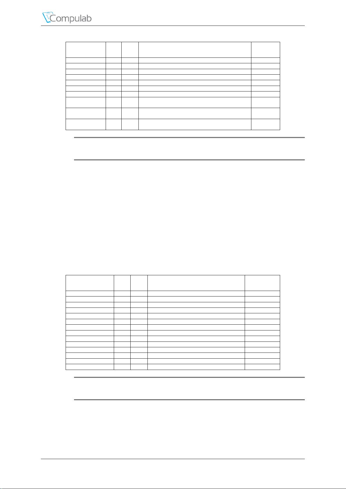
Please refer to the AM57x Reference manual for additional details. The table below summarizes
the HDMI interface signals
Table 6 HDMI Interface Signals
NOTE: Pins denoted with "*" are multifunctional. For additional details please refer to
chapter 5.5 of this document
4.1.3 LVDS Display interface
LVDS interface is derived from an on-board SN75LVDS83B FlatLink™ transmitter. The
transmitter is interfaced with the AM57x Parallel RGB interface "vout3". The LVDS transmitter
supports the following key features:
Revised April 2018 CL-SOM-AM57x 18
Page 19
Peripheral Interfaces
Signal Name
Pin
#
Type
Description
Availability
LVDS_CLKN
33
ODS
Differential LVDS pixel clock output, highimpedance when device in SHTDN
With "C1500D"
AND "L"
LVDS_CLKP
35
ODS
Differential LVDS pixel clock output, highimpedance when device in SHTDN
With "C1500D"
AND "L"
LVDS_N0
41
ODS
Differential LVDS data output, high-impedance
when device in SHTDN
With "C1500D"
AND "L"
LVDS_N1
47
ODS
Differential LVDS data output, high-impedance
when device in SHTDN
With "C1500D"
AND "L"
LVDS_N2
53
ODS
Differential LVDS data output, high-impedance
when device in SHTDN
With "C1500D"
AND "L"
LVDS_N3
59
ODS
Differential LVDS data output, high-impedance
when device in SHTDN
With "C1500D"
AND "L"
LVDS_P0
39
ODS
Differential LVDS data output, high-impedance
when device in SHTDN
With "C1500D"
AND "L"
LVDS_P1
45
ODS
Differential LVDS data output, high-impedance
when device in SHTDN
With "C1500D"
AND "L"
LVDS_P2
51
ODS
Differential LVDS data output, high-impedance
when device in SHTDN
With "C1500D"
AND "L"
LVDS_P3
57
ODS
Differential LVDS data output, high-impedance
when device in SHTDN
With "C1500D"
AND "L"
Transfer rate up to 135 Mpps, pixel clock frequency range 10 MHz to135 MHz
Suited for display resolutions ranging from HVGA up to HD with low EMI
Operates From a Single 3.3-V Supply
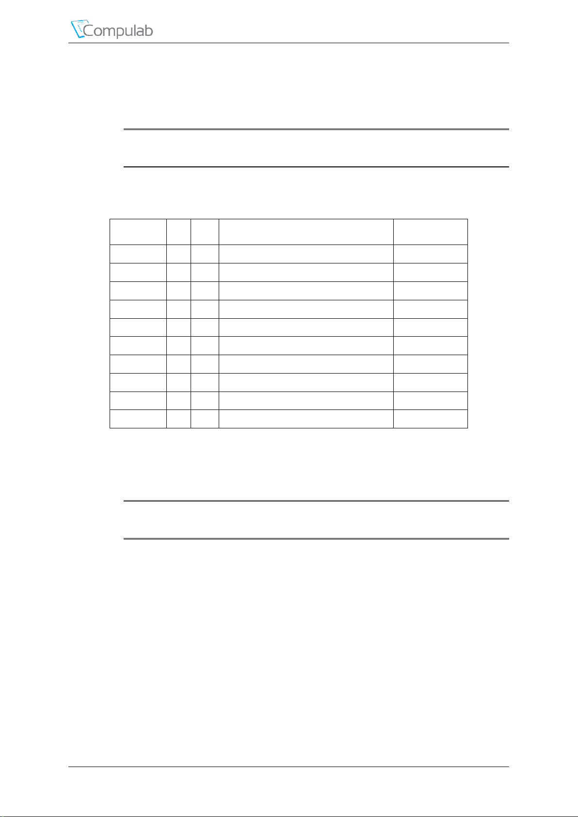
NOTE: CL-SOM-AM57x LVDS display interface is available only with the ‘L’ and
'C1500D' ordering option.
For additional details on the LVDS Transmitter, please refer to the TI SN75LVDS83B datasheet.
The table below summarizes the LVDS interface signals
Table 7 LVDS Interface Signals
4.2 Parallel Camera Interface
The camera interface available with CL-SOM-AM57x is based on the AM57x integrated Video
Input Port (VIP) modules.
NOTE: All of the Camera interface pins on CL-SOM-AM57x are multifunctional. For
additional details please refer to chapter 5.5 of this document.
With C1500D option (AM5728) there are 3 instantiations of the VIP (VIP1, VIP2, and VIP3) for
connection to CCD cameras or BT656 compliant video encoders. On CL-SOM-AM57x based on
"C1500D" the following main features are supported:
VIP1 module with support of:
One 8-bit video port for parallel RGB/YUV/RAW data, up to 165 MHz
VIP2 module with support of:
One 24-bit video port for parallel RGB/YUV/RAW data, up to 165 MHz
One 8-bit (out of 24) video port for parallel RGB/YUV/RAW data, up to 165
MHz
VIP3 module with support of:
One 16-bit video port for parallel RGB/YUV/RAW data, up to 165 MHz
With C1500 option (AM5718) there is one instantiations of the VIP (VIP1) for connection to
CCD cameras or BT656 compliant video encoders. On CL-SOM-AM57x based on "C1500" the
following main features are supported:
Revised April 2018 CL-SOM-AM57x 19
Page 20
Peripheral Interfaces
Signal Name
Pin
#
Type
Description
Availability
VIN1A_CLK0
49* I Video Input 1 Port A Clock input
With "C1500"
VIN1A_CLK0
161* I Video Input 1 Port A Clock input
With "C1500"
VIN1A_CLK0
193* I Video Input 1 Port A Clock input
With "C1500" AND Without
"A"
VIN1A_CLK0
95* I Video Input 1 Port A Clock input
With "C1500"
VIN1A_CLK0
161* I Video Input 1 Port A Clock input
With "C1500"
VIN1A_CLK0
154 I Video Input 1 Port A Clock input
With "C1500"
VIN1A_D0
94* I Video Input 1 Port A Data input
With "C1500"
VIN1A_D0
101* I Video Input 1 Port A Data input
With "C1500"
VIN1A_D0
163* I Video Input 1 Port A Data input
With "C1500"
VIN1A_D0
197* I Video Input 1 Port A Data input
With "C1500" AND Without
"A"
VIN1A_D0
152 I Video Input 1 Port A Data input
With "C1500"
VIN1A_D1
92* I Video Input 1 Port A Data input
With "C1500"
VIN1A_D1
103* I Video Input 1 Port A Data input
With "C1500"
VIN1A_D1
202* I Video Input 1 Port A Data input
With "C1500"
VIN1A_D1
201 I Video Input 1 Port A Data input
With "C1500" AND Without
"A"
VIN1A_D10
128* I Video Input 1 Port A Data input
With "C1500"
VIN1A_D10
139* I Video Input 1 Port A Data input
With "C1500"
VIN1A_D11
5* I Video Input 1 Port A Data input
With "C1500"
VIN1A_D11
130* I Video Input 1 Port A Data input
With "C1500"
VIN1A_D11
143* I Video Input 1 Port A Data input
With "C1500"
VIN1A_D12
17* I Video Input 1 Port A Data input
With "C1500"
VIN1A_D12
134* I Video Input 1 Port A Data input
With "C1500"
VIN1A_D13
15* I Video Input 1 Port A Data input
With "C1500"
VIN1A_D13
136* I Video Input 1 Port A Data input
With "C1500"
VIN1A_D14
11* I Video Input 1 Port A Data input
With "C1500"
VIN1A_D14
138* I Video Input 1 Port A Data input
With "C1500"
VIN1A_D15
13* I Video Input 1 Port A Data input
With "C1500"
VIN1A_D15
140* I Video Input 1 Port A Data input
With "C1500"
VIN1A_D16
13* I Video Input 1 Port A Data input
With "C1500"
VIN1A_D16
101* I Video Input 1 Port A Data input
With "C1500"
VIN1A_D16
106* I Video Input 1 Port A Data input
With "C1500"
VIN1A_D17
11* I Video Input 1 Port A Data input
With "C1500"
VIN1A_D17
103* I Video Input 1 Port A Data input
With "C1500"
VIN1A_D17
108* I Video Input 1 Port A Data input
With "C1500"
VIN1A_D18
15* I Video Input 1 Port A Data input
With "C1500"
VIN1A_D18
89* I Video Input 1 Port A Data input
With "C1500"
VIN1A_D18
110* I Video Input 1 Port A Data input
With "C1500"
VIN1A_D19
17* I Video Input 1 Port A Data input
With "C1500"
VIN1A_D19
91* I Video Input 1 Port A Data input
With "C1500"
VIN1A_D19
112* I Video Input 1 Port A Data input
With "C1500"
VIN1A_D2
52* I Video Input 1 Port A Data input
With "C1500"
VIN1A_D2
89* I Video Input 1 Port A Data input
With "C1500"
VIN1A_D2
142* I Video Input 1 Port A Data input
With "C1500"
VIN1A_D2
203 I Video Input 1 Port A Data input
With "C1500" AND Without
"A"
VIN1A_D20
5* I Video Input 1 Port A Data input
With "C1500"
VIN1A_D20
77* I Video Input 1 Port A Data input
With "C1500"
VIN1A_D20
116* I Video Input 1 Port A Data input
With "C1500"
VIN1A_D21
3* I Video Input 1 Port A Data input
With "C1500"
VIN1A_D21
79* I Video Input 1 Port A Data input
With "C1500"
VIN1A_D21
118* I Video Input 1 Port A Data input
With "C1500"
VIN1A_D22
7* I Video Input 1 Port A Data input
With "C1500"
VIN1A_D22
83* I Video Input 1 Port A Data input
With "C1500"
VIN1A_D22
120* I Video Input 1 Port A Data input
With "C1500"
VIN1A_D23
9* I Video Input 1 Port A Data input
With "C1500"
VIN1A_D23
85* I Video Input 1 Port A Data input
With "C1500"
VIN1A_D23
122* I Video Input 1 Port A Data input
With "C1500"
One separate 24-bit video ports for parallel RGB/YUV/RAW data, up to 165 MHz
One separate 8-bit video ports for YUV/RAW data, up to 165 MHz
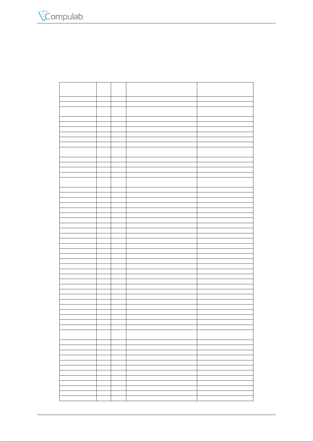
For additional details on VIP modules, please refer to the AM572x or AM571x technical
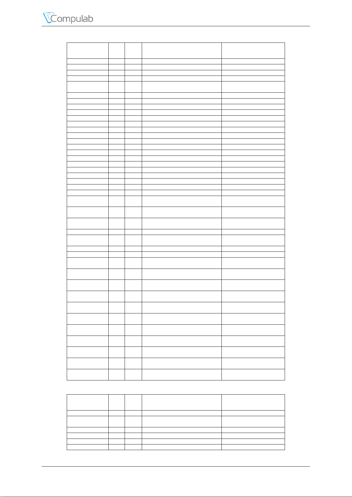
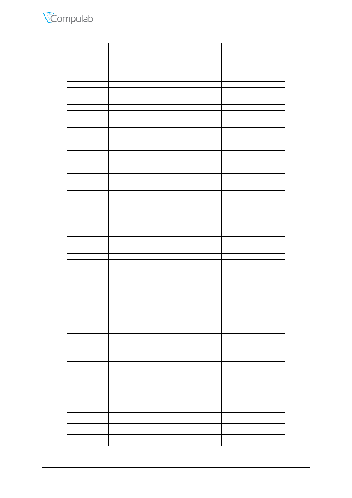
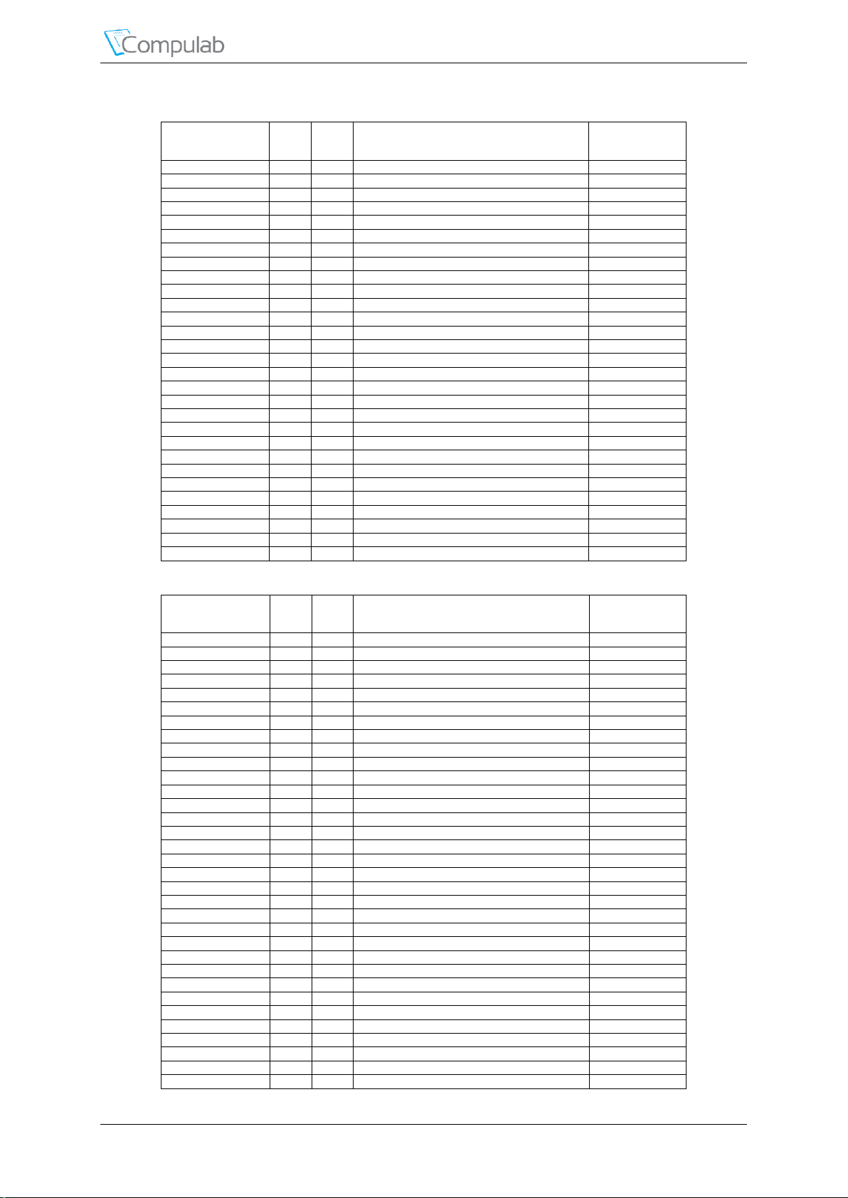
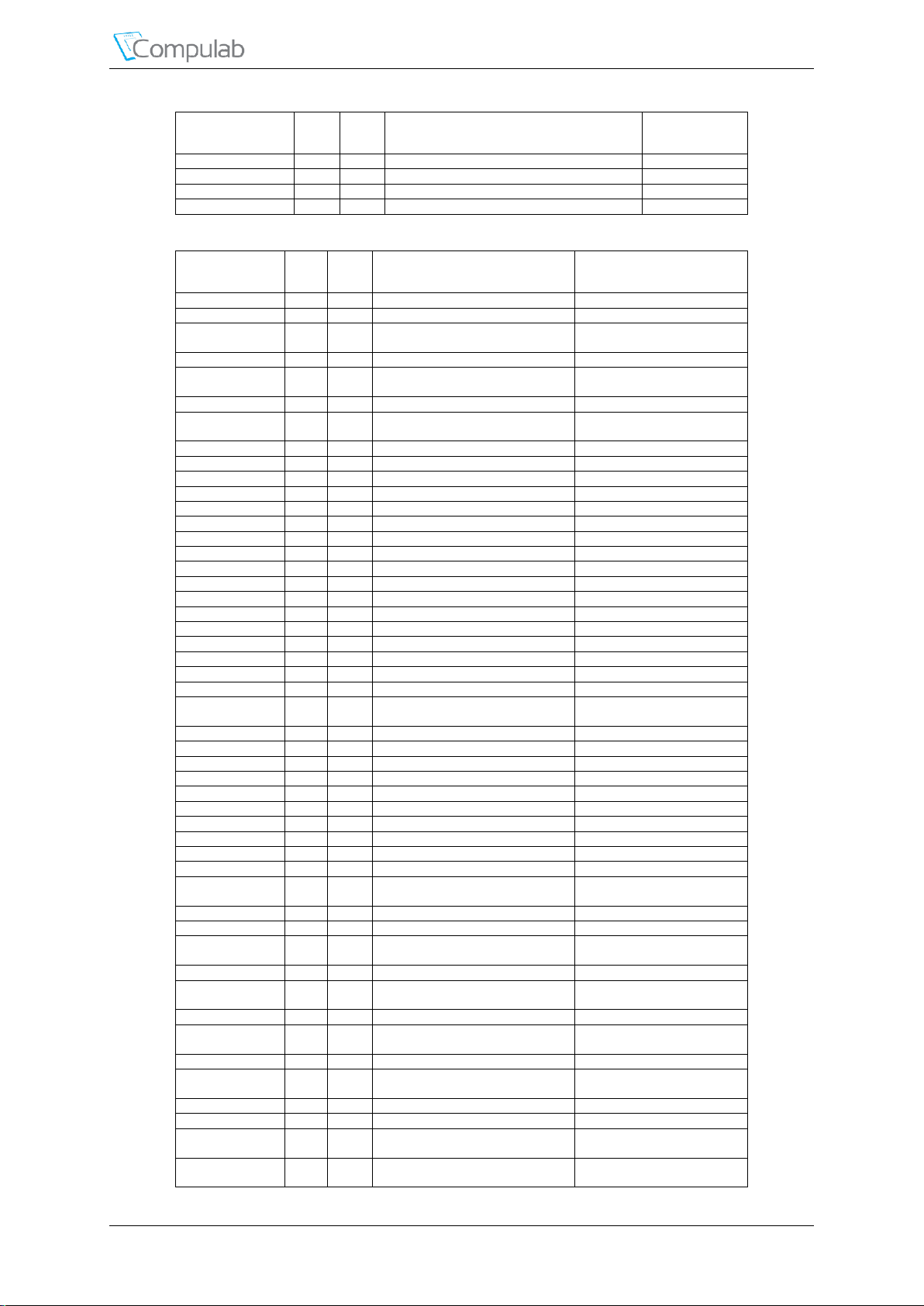
reference manual. The tables below summarize the Parallel camera interface signals
Table 8 Parallel camera VIN1A Interface Signals
Revised April 2018 CL-SOM-AM57x 20
Page 21
Peripheral Interfaces
Signal Name
Pin
#
Type
Description
Availability
VIN1A_D3
58* I Video Input 1 Port A Data input
With "C1500"
VIN1A_D3
91* I Video Input 1 Port A Data input
With "C1500"
VIN1A_D3
144* I Video Input 1 Port A Data input
With "C1500"
VIN1A_D3
174* I Video Input 1 Port A Data input
With "C1500"
VIN1A_D3
199 I Video Input 1 Port A Data input
With "C1500" AND Without
"A"
VIN1A_D4
65* I Video Input 1 Port A Data input
With "C1500"
VIN1A_D4
77* I Video Input 1 Port A Data input
With "C1500"
VIN1A_D4
146* I Video Input 1 Port A Data input
With "C1500"
VIN1A_D5
63* I Video Input 1 Port A Data input
With "C1500"
VIN1A_D5
79* I Video Input 1 Port A Data input
With "C1500"
VIN1A_D5
148* I Video Input 1 Port A Data input
With "C1500"
VIN1A_D6
69* I Video Input 1 Port A Data input
With "C1500"
VIN1A_D6
74* I Video Input 1 Port A Data input
With "C1500"
VIN1A_D6
83* I Video Input 1 Port A Data input
With "C1500"
VIN1A_D6
145 I Video Input 1 Port A Data input
With "C1500"
VIN1A_D7
75* I Video Input 1 Port A Data input
With "C1500"
VIN1A_D7
76* I Video Input 1 Port A Data input
With "C1500"
VIN1A_D7
85* I Video Input 1 Port A Data input
With "C1500"
VIN1A_D7
137 I Video Input 1 Port A Data input
With "C1500"
VIN1A_D8
9* I Video Input 1 Port A Data input
With "C1500"
VIN1A_D8
124* I Video Input 1 Port A Data input
With "C1500"
VIN1A_D9
7* I Video Input 1 Port A Data input
With "C1500"
VIN1A_D9
126* I Video Input 1 Port A Data input
With "C1500"
VIN1A_DE0
43*
I
Video Input 1 Port A Data Enable
input
With "C1500"
VIN1A_DE0
97*
I
Video Input 1 Port A Data Enable
input
With "C1500"
VIN1A_DE0
104*
I
Video Input 1 Port A Data Enable
input
With "C1500"
VIN1A_FLD0
98* I Video Input 1 Port A Field ID input
With "C1500"
VIN1A_FLD0
197* I Video Input 1 Port A Field ID input
With "C1500" AND Without
"A"
VIN1A_FLD0
98* I Video Input 1 Port A Field ID input
With "C1500"
VIN1A_FLD0
99* I Video Input 1 Port A Field ID input
With "C1500"
VIN1A_HSYNC0
194*
I
Video Input 1 Port A Horizontal Sync
input
With "C1500"
VIN1A_HSYNC0
100*
I
Video Input 1 Port A Horizontal Sync
input
With "C1500"
VIN1A_HSYNC0
102*
I
Video Input 1 Port A Horizontal Sync
input
With "C1500"
VIN1A_HSYNC0
115*
I
Video Input 1 Port A Horizontal Sync
input
With "C1500"
VIN1A_HSYNC0
129
I
Video Input 1 Port A Horizontal Sync
input
With "C1500"
VIN1A_VSYNC0
179*
I
Video Input 1 Port A Vertical Sync
input
With "C1500"
VIN1A_VSYNC0
100*
I
Video Input 1 Port A Vertical Sync
input
With "C1500"
VIN1A_VSYNC0
102*
I
Video Input 1 Port A Vertical Sync
input
With "C1500"
VIN1A_VSYNC0
81*
I
Video Input 1 Port A Vertical Sync
input
With "C1500"
VIN1A_VSYNC0
135
I
Video Input 1 Port A Vertical Sync
input
With "C1500"
VIN1A_VSYNC1
113*
I
Video Input 1 Port A Vertical Sync
input
With "C1500"
Signal Name
Pin
#
Type
Description
Availability
VIN2A_CLK0
161* I Video Input 2 Port A Clock input
With "C1500"
VIN2A_CLK0
193* I Video Input 2 Port A Clock input
With "C1500" AND Without
"A"
VIN2A_CLK0
95* I Video Input 2 Port A Clock input
With "C1500"
VIN2A_D0
94* I Video Input 2 Port A Data input
With "C1500"
VIN2A_D0
101* I Video Input 2 Port A Data input
With "C1500"
VIN2A_D1
92* I Video Input 2 Port A Data input
With "C1500"
Revised April 2018 CL-SOM-AM57x 21
Table 9 Parallel camera VIN2A Interface Signals
Page 22
Peripheral Interfaces
Signal Name
Pin
#
Type
Description
Availability
VIN2A_D1
103* I Video Input 2 Port A Data input
With "C1500"
VIN2A_D1
117 I Video Input 2 Port A Data input
With "C1500D"
VIN2A_D1
117 I Video Input 2 Port A Data input
With "C1500"
VIN2A_D10
139* I Video Input 2 Port A Data input
With "C1500"
VIN2A_D10
128* I Video Input 2 Port A Data input
With "C1500"
VIN2A_D11
143* I Video Input 2 Port A Data input
With "C1500"
VIN2A_D11
130* I Video Input 2 Port A Data input
With "C1500"
VIN2A_D12
134* I Video Input 2 Port A Data input
With "C1500"
VIN2A_D13
136* I Video Input 2 Port A Data input
With "C1500"
VIN2A_D14
138* I Video Input 2 Port A Data input
With "C1500"
VIN2A_D15
140* I Video Input 2 Port A Data input
With "C1500"
VIN2A_D16
13* I Video Input 2 Port A Data input
With "C1500"
VIN2A_D16
106* I Video Input 2 Port A Data input
With "C1500"
VIN2A_D17
11* I Video Input 2 Port A Data input
With "C1500"
VIN2A_D17
108* I Video Input 2 Port A Data input
With "C1500"
VIN2A_D18
110* I Video Input 2 Port A Data input
With "C1500"
VIN2A_D18
15* I Video Input 2 Port A Data input
With "C1500"
VIN2A_D19
17* I Video Input 2 Port A Data input
With "C1500"
VIN2A_D19
112* I Video Input 2 Port A Data input
With "C1500"
VIN2A_D2
142* I Video Input 2 Port A Data input
With "C1500"
VIN2A_D2
89* I Video Input 2 Port A Data input
With "C1500"
VIN2A_D2
111 I Video Input 2 Port A Data input
With "C1500D"
VIN2A_D2
111 I Video Input 2 Port A Data input
With "C1500"
VIN2A_D20
5* I Video Input 2 Port A Data input
With "C1500"
VIN2A_D20
116* I Video Input 2 Port A Data input
With "C1500"
VIN2A_D21
3* I Video Input 2 Port A Data input
With "C1500"
VIN2A_D21
118* I Video Input 2 Port A Data input
With "C1500"
VIN2A_D22
7* I Video Input 2 Port A Data input
With "C1500"
VIN2A_D22
120* I Video Input 2 Port A Data input
With "C1500"
VIN2A_D23
9* I Video Input 2 Port A Data input
With "C1500"
VIN2A_D23
122* I Video Input 2 Port A Data input
With "C1500"
VIN2A_D3
144* I Video Input 2 Port A Data input
With "C1500"
VIN2A_D3
174* I Video Input 2 Port A Data input
With "C1500"
VIN2A_D3
91* I Video Input 2 Port A Data input
With "C1500"
VIN2A_D4
146* I Video Input 2 Port A Data input
With "C1500"
VIN2A_D4
77* I Video Input 2 Port A Data input
With "C1500"
VIN2A_D5
148* I Video Input 2 Port A Data input
With "C1500"
VIN2A_D5
79* I Video Input 2 Port A Data input
With "C1500"
VIN2A_D6
74* I Video Input 2 Port A Data input
With "C1500"
VIN2A_D6
83* I Video Input 2 Port A Data input
With "C1500"
VIN2A_D7
76* I Video Input 2 Port A Data input
With "C1500"
VIN2A_D7
85* I Video Input 2 Port A Data input
With "C1500"
VIN2A_D8
124* I Video Input 2 Port A Data input
With "C1500"
VIN2A_D9
126* I Video Input 2 Port A Data input
With "C1500"
VIN2A_DE0
104*
I
Video Input 2 Port A Data Enable
input
With "C1500"
VIN2A_DE0
97*
I
Video Input 2 Port A Data Enable
input
With "C1500"
VIN2A_DE0
93*
I
Video Input 2 Port A Data Enable
input
With "C1500D"
VIN2A_DE0
93*
I
Video Input 2 Port A Data Enable
input
With "C1500"
VIN2A_FLD0
98* I Video Input 2 Port A Field ID input
With "C1500"
VIN2A_FLD0
99* I Video Input 2 Port A Field ID input
With "C1500"
VIN2A_FLD0
93* I Video Input 2 Port A Field ID input
With "C1500D"
VIN2A_FLD0
93* I Video Input 2 Port A Field ID input
With "C1500"
VIN2A_HSYNC0
102*
I
Video Input 2 Port A Horizontal Sync
input
With "C1500"
VIN2A_HSYNC0
115*
I
Video Input 2 Port A Horizontal Sync
input
With "C1500"
VIN2A_VSYNC0
100*
I
Video Input 2 Port A Horizontal Sync
input
With "C1500"
VIN2A_VSYNC0
113*
I
Video Input 2 Port A Vertical Sync
input
With "C1500"
VIN2A_VSYNC0
73*
I
Video Input 2 Port A Vertical Sync
input
With "C1500D"
VIN2A_VSYNC0
81*
I
Video Input 2 Port A Vertical Sync
input
With "C1500"
Revised April 2018 CL-SOM-AM57x 22
Page 23
Peripheral Interfaces
Signal Name
Pin
#
Type
Description
Availability
VIN2B_CLK1
179* I Video Input 2 Port B Clock input
With "C1500D"
VIN2B_CLK1
179* I Video Input 2 Port B Clock input
With "C1500"
VIN2B_D0
163* I Video Input 2 Port B Data input
With "C1500D"
VIN2B_D0
163* I Video Input 2 Port B Data input
With "C1500"
VIN2B_D1
202* I Video Input 2 Port B Data input
With "C1500D"
VIN2B_D1
202* I Video Input 2 Port B Data input
With "C1500"
VIN2B_D2
52* I Video Input 2 Port B Data input
With "C1500D"
VIN2B_D2
52* I Video Input 2 Port B Data input
With "C1500"
VIN2B_D3
58* I Video Input 2 Port B Data input
With "C1500D"
VIN2B_D3
58* I Video Input 2 Port B Data input
With "C1500"
VIN2B_D4
65* I Video Input 2 Port B Data input
With "C1500D"
VIN2B_D4
65* I Video Input 2 Port B Data input
With "C1500"
VIN2B_D5
63* I Video Input 2 Port B Data input
With "C1500D"
VIN2B_D5
63* I Video Input 2 Port B Data input
With "C1500"
VIN2B_D6
69* I Video Input 2 Port B Data input
With "C1500D"
VIN2B_D6
69* I Video Input 2 Port B Data input
With "C1500"
VIN2B_D7
75* I Video Input 2 Port B Data input
With "C1500D"
VIN2B_D7
75* I Video Input 2 Port B Data input
With "C1500"
VIN2B_DE1
194* I Video Input 2 Port B Data Enable input
With "C1500D"
VIN2B_DE1
194* I Video Input 2 Port B Data Enable input
With "C1500"
VIN2B_DE1
93* I Video Input 2 Port B Data Enable input
With "C1500D"
VIN2B_DE1
93* I Video Input 2 Port B Data Enable input
With "C1500"
VIN2B_FLD1
93* I Video Input 2 Port B Field ID input
With "C1500D"
VIN2B_FLD1
93* I Video Input 2 Port B Field ID input
With "C1500"
VIN2B_HSYNC1
49* I Video Input 2 Port B Horizontal Sync input
With "C1500D"
VIN2B_HSYNC1
49* I Video Input 2 Port B Horizontal Sync input
With "C1500"
VIN2B_VSYNC1
43* I Video Input 2 Port B Vertical Sync input
With "C1500D"
VIN2B_VSYNC1
73* I Video Input 2 Port B Vertical Sync input
With "C1500D"
VIN2B_VSYNC2
43* I Video Input 2 Port B Vertical Sync input
With "C1500"
Signal Name
Pin
#
Type
Description
Availability
VIN3A_CLK0
161* I Video Input 3 Port A Clock input
With "C1500D"
VIN3A_D0
94* I Video Input 3 Port A Data input
With "C1500D"
VIN3A_D1
92* I Video Input 3 Port A Data input
With "C1500D"
VIN3A_D10
128* I Video Input 3 Port A Data input
With "C1500D"
VIN3A_D11
130* I Video Input 3 Port A Data input
With "C1500D"
VIN3A_D12
134* I Video Input 3 Port A Data input
With "C1500D"
VIN3A_D13
136* I Video Input 3 Port A Data input
With "C1500D"
VIN3A_D14
138* I Video Input 3 Port A Data input
With "C1500D"
VIN3A_D15
140* I Video Input 3 Port A Data input
With "C1500D"
VIN3A_D16
106* I Video Input 3 Port A Data input
With "C1500D"
VIN3A_D16
101 I Video Input 3 Port A Data input
With "C1500D"
VIN3A_D17
108* I Video Input 3 Port A Data input
With "C1500D"
VIN3A_D17
103 I Video Input 3 Port A Data input
With "C1500D"
VIN3A_D18
110* I Video Input 3 Port A Data input
With "C1500D"
VIN3A_D18
89 I Video Input 3 Port A Data input
With "C1500D"
VIN3A_D19
112* I Video Input 3 Port A Data input
With "C1500D"
VIN3A_D19
91 I Video Input 3 Port A Data input
With "C1500D"
VIN3A_D2
142* I Video Input 3 Port A Data input
With "C1500D"
VIN3A_D20
116* I Video Input 3 Port A Data input
With "C1500D"
VIN3A_D20
77 I Video Input 3 Port A Data input
With "C1500D"
VIN3A_D21
118* I Video Input 3 Port A Data input
With "C1500D"
VIN3A_D21
79 I Video Input 3 Port A Data input
With "C1500D"
VIN3A_D22
120* I Video Input 3 Port A Data input
With "C1500D"
VIN3A_D22
83 I Video Input 3 Port A Data input
With "C1500D"
VIN3A_D23
122* I Video Input 3 Port A Data input
With "C1500D"
VIN3A_D23
85 I Video Input 3 Port A Data input
With "C1500D"
VIN3A_D3
144* I Video Input 3 Port A Data input
With "C1500D"
VIN3A_D4
146* I Video Input 3 Port A Data input
With "C1500D"
VIN3A_D5
148* I Video Input 3 Port A Data input
With "C1500D"
VIN3A_D6
74* I Video Input 3 Port A Data input
With "C1500D"
VIN3A_D7
76* I Video Input 3 Port A Data input
With "C1500D"
VIN3A_D8
124* I Video Input 3 Port A Data input
With "C1500D"
VIN3A_D9
126* I Video Input 3 Port A Data input
With "C1500D"
Table 10 Parallel camera VIN2B Interface Signals
Table 11 Parallel camera VIN3A Interface Signals
Revised April 2018 CL-SOM-AM57x 23
Page 24
Peripheral Interfaces
Signal Name
Pin
#
Type
Description
Availability
VIN3A_DE0
104* I Video Input 3 Port A Data Enable input
With "C1500D"
VIN3A_FLD0
98* I Video Input 3 Port A Field ID input
With "C1500D"
VIN3A_HSYNC0
100* I Video Input 3 Port A Horizontal Sync input
With "C1500D"
VIN3A_VSYNC0
102* I Video Input 3 Port A Vertical Sync input
With "C1500D"
Signal Name
Pin
#
Type
Description
Availability
VIN4A_CLK0
161* I Video Input 4 Port A Clock input
With "C1500D"
VIN4A_CLK0
95 I Video Input 4 Port A Clock input
With "C1500D"
VIN4A_CLK0
193 I Video Input 4 Port A Clock input
With "C1500D" AND Without
"A"
VIN4A_D0
94* I Video Input 4 Port A Data input
With "C1500D"
VIN4A_D0
101 I Video Input 4 Port A Data input
With "C1500D" AND Without
"E2"
VIN4A_D1
92* I Video Input 4 Port A Data input
With "C1500D"
VIN4A_D1
103 I Video Input 4 Port A Data input
With "C1500D" AND Without
"E2"
VIN4A_D10
128* I Video Input 4 Port A Data input
With "C1500D"
VIN4A_D10
139 I Video Input 4 Port A Data input
With "C1500D"
VIN4A_D11
130* I Video Input 4 Port A Data input
With "C1500D"
VIN4A_D11
143 I Video Input 4 Port A Data input
With "C1500D"
VIN4A_D12
134* I Video Input 4 Port A Data input
With "C1500D"
VIN4A_D13
136* I Video Input 4 Port A Data input
With "C1500D"
VIN4A_D14
138* I Video Input 4 Port A Data input
With "C1500D"
VIN4A_D15
140* I Video Input 4 Port A Data input
With "C1500D"
VIN4A_D16
13* I Video Input 4 Port A Data input
With "C1500D"
VIN4A_D16
106* I Video Input 4 Port A Data input
With "C1500D"
VIN4A_D17
11* I Video Input 4 Port A Data input
With "C1500D"
VIN4A_D17
108* I Video Input 4 Port A Data input
With "C1500D"
VIN4A_D18
110* I Video Input 4 Port A Data input
With "C1500D"
VIN4A_D18
15* I Video Input 4 Port A Data input
With "C1500D"
VIN4A_D19
17* I Video Input 4 Port A Data input
With "C1500D"
VIN4A_D19
112* I Video Input 4 Port A Data input
With "C1500D"
VIN4A_D2
142* I Video Input 4 Port A Data input
With "C1500D"
VIN4A_D2
89 I Video Input 4 Port A Data input
With "C1500D" AND Without
"E2"
VIN4A_D2
162 I Video Input 4 Port A Data input
With "C1500D"
VIN4A_D20
5* I Video Input 4 Port A Data input
With "C1500D"
VIN4A_D20
116* I Video Input 4 Port A Data input
With "C1500D"
VIN4A_D21
3* I Video Input 4 Port A Data input
With "C1500D"
VIN4A_D21
118* I Video Input 4 Port A Data input
With "C1500D"
VIN4A_D22
7* I Video Input 4 Port A Data input
With "C1500D"
VIN4A_D22
120* I Video Input 4 Port A Data input
With "C1500D"
VIN4A_D23
9* I Video Input 4 Port A Data input
With "C1500D"
VIN4A_D23
122* I Video Input 4 Port A Data input
With "C1500D"
VIN4A_D3
144* I Video Input 4 Port A Data input
With "C1500D"
VIN4A_D3
91 I Video Input 4 Port A Data input
With "C1500D" AND Without
"E2"
VIN4A_D3
174 I Video Input 4 Port A Data input
With "C1500D"
VIN4A_D4
146* I Video Input 4 Port A Data input
With "C1500D"
VIN4A_D4
77 I Video Input 4 Port A Data input
With "C1500D" AND Without
"E2"
VIN4A_D5
148* I Video Input 4 Port A Data input
With "C1500D"
VIN4A_D5
79 I Video Input 4 Port A Data input
With "C1500D" AND Without
"E2"
VIN4A_D6
74* I Video Input 4 Port A Data input
With "C1500D"
VIN4A_D6
83 I Video Input 4 Port A Data input
With "C1500D" AND Without
"E2"
VIN4A_D7
76* I Video Input 4 Port A Data input
With "C1500D"
VIN4A_D7
85 I Video Input 4 Port A Data input
With "C1500D" AND Without
"E2"
VIN4A_D8
124* I Video Input 4 Port A Data input
With "C1500D"
VIN4A_D9
126* I Video Input 4 Port A Data input
With "C1500D"
VIN4A_DE0
104*
I
Video Input 4 Port A Data Enable
input
With "C1500D"
VIN4A_DE0
97
I
Video Input 4 Port A Data Enable
input
With "C1500D"
Table 12 Parallel camera VIN4A Interface Signals
Revised April 2018 CL-SOM-AM57x 24
Page 25
Peripheral Interfaces
Signal Name
Pin
#
Type
Description
Availability
VIN4A_FLD0
98* I Video Input 4 Port A Field ID input
With "C1500D"
VIN4A_FLD0
99 I Video Input 4 Port A Field ID input
With "C1500D"
VIN4A_HSYNC0
100*
I
Video Input 4 Port A Horizontal
Sync input
With "C1500D"
VIN4A_HSYNC0
115
I
Video Input 4 Port A Horizontal
Sync input
With "C1500D"
VIN4A_VSYNC0
102*
I
Video Input 4 Port A Vertical Sync
input
With "C1500D"
VIN4A_VSYNC0
81
I
Video Input 4 Port A Vertical Sync
input
With "C1500D"
VIN4A_VSYNC0
113
I
Video Input 4 Port A Vertical Sync
input
With "C1500D"
Signal Name
Pin
#
Type
Description
Availability
VIN5A_CLK0
49* I Video Input 5 Port A Clock input
With "C1500D"
VIN5A_D0
163* I Video Input 5 Port A Data input
With "C1500D"
VIN5A_D1
202* I Video Input 5 Port A Data input
With "C1500D"
VIN5A_D10
3* I Video Input 5 Port A Data input
With "C1500D"
VIN5A_D11
5* I Video Input 5 Port A Data input
With "C1500D"
VIN5A_D12
17* I Video Input 5 Port A Data input
With "C1500D"
VIN5A_D13
15* I Video Input 5 Port A Data input
With "C1500D"
VIN5A_D14
11* I Video Input 5 Port A Data input
With "C1500D"
VIN5A_D15
13* I Video Input 5 Port A Data input
With "C1500D"
VIN5A_D2
52* I Video Input 5 Port A Data input
With "C1500D"
VIN5A_D3
58* I Video Input 5 Port A Data input
With "C1500D"
VIN5A_D4
65* I Video Input 5 Port A Data input
With "C1500D"
VIN5A_D5
63* I Video Input 5 Port A Data input
With "C1500D"
VIN5A_D6
69* I Video Input 5 Port A Data input
With "C1500D"
VIN5A_D7
75* I Video Input 5 Port A Data input
With "C1500D"
VIN5A_D8
9* I Video Input 5 Port A Data input
With "C1500D"
VIN5A_D9
7* I Video Input 5 Port A Data input
With "C1500D"
VIN5A_DE0
43*
I
Video Input 5 Port A Data Enable
input
With "C1500D"
VIN5A_FLD0
197 I Video Input 5 Port A Field ID input
With "C1500D" AND
Without "A"
VIN5A_HSYNC0
194*
I
Video Input 5 Port A Horizontal
Sync input
With "C1500D"
VIN5A_VSYNC0
179*
I
Video Input 5 Port A Vertical Sync
input
With "C1500D"
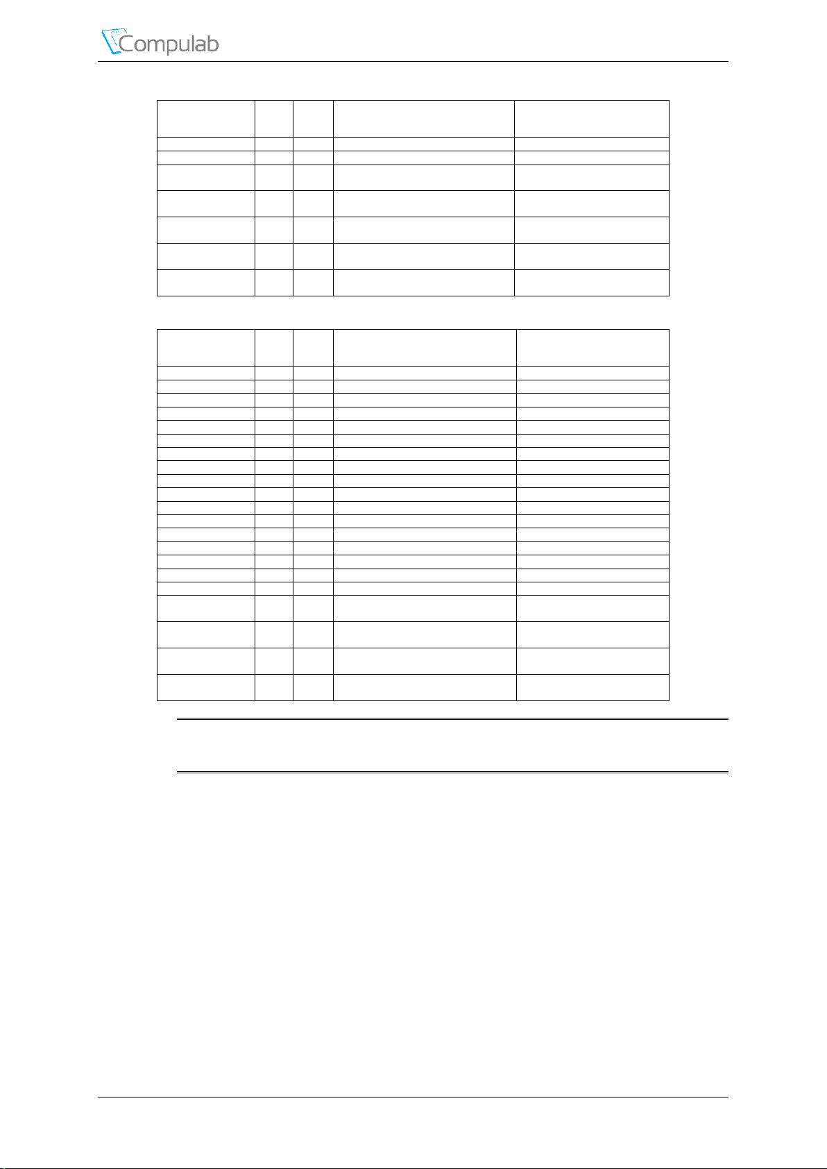
Table 13 Parallel camera VIN5A Interface Signals
NOTE: Pins denoted with "*" are multifunctional. For additional details please refer to
chapter 5.5 of this document
Revised April 2018 CL-SOM-AM57x 25
Page 26
Peripheral Interfaces
Signal
Name
Pin
#
Type
Description
Availability
LJCB_CLKN
121
IODS
PCIe1_PHY / PCIe2_PHY shared Reference Clock Input /
Output Differential Pair (negative)
Always
LJCB_CLKP
119
IODS
PCIe1_PHY / PCIe2_PHY shared Reference Clock Input /
Output Differential Pair (positive)
Always
PCIE_RXN0
133
IDS
PCIe1_PHY_RX Receive Data Lane 0 (negative) - mapped
to PCIe_SS1 only
Always
PCIE_RXN1
167
IDS
PCIe2_PHY_RX Receive Data Lane 1 (negative) - mapped
to either PCIe_SS1 (dual lane- mode) or PCIe_SS2 (single
lane- mode)
With
"C1500D"
PCIE_RXN1
184
IDS
PCIe2_PHY_RX Receive Data Lane 1 (negative) AM5718
ONLY
With
"C1500"
PCIE_RXP0
131
IDS
PCIe1_PHY_RX Receive Data Lane 0 (positive) - mapped
to PCIe_SS1 only
Always
PCIE_RXP1
169
IDS
PCIe2_PHY_RX Receive Data Lane 1 (positive) - mapped
to either PCIe_SS1 (dual lane- mode) or PCIe_SS2 (single
lane- mode)
With
"C1500D"
PCIE_RXP1
182
IDS
PCIe2_PHY_RX Receive Data Lane 1 (positive) AM5718
ONLY
With
"C1500"
PCIE_TXN0
127
ODS
PCIe1_PHY_TX Transmit Data Lane 0 (negative) - mapped
to PCIe_SS1 only
Always
PCIE_TXN1
173
ODS
PCIe2_PHY_TX Transmit Data Lane 1 (negative) - mapped
to either PCIe_SS1 (dual lane- mode) or PCIe_SS2 (single
lane- mode)
With
"C1500D"
PCIE_TXN1
190
ODS
PCIe2_PHY_TX Transmit Data Lane 1 (negative) AM5718
ONLY
With
"C1500"
PCIE_TXP0
125
ODS
PCIe1_PHY_TX Transmit Data Lane 0 (positive) - mapped
to PCIe_SS1 only
Always
PCIE_TXP1
175
ODS
PCIe2_PHY_TX Transmit Data Lane 1 (positive) - mapped
to either PCIe_SS1 (dual lane- mode) or PCIe_SS2 (single
lane- mode)
With
"C1500D"
PCIE_TXP1
188
ODS
PCIe2_PHY_TX Transmit Data Lane 1 (positive) AM5718
ONLY
With
"C1500"
4.3 PCI Express
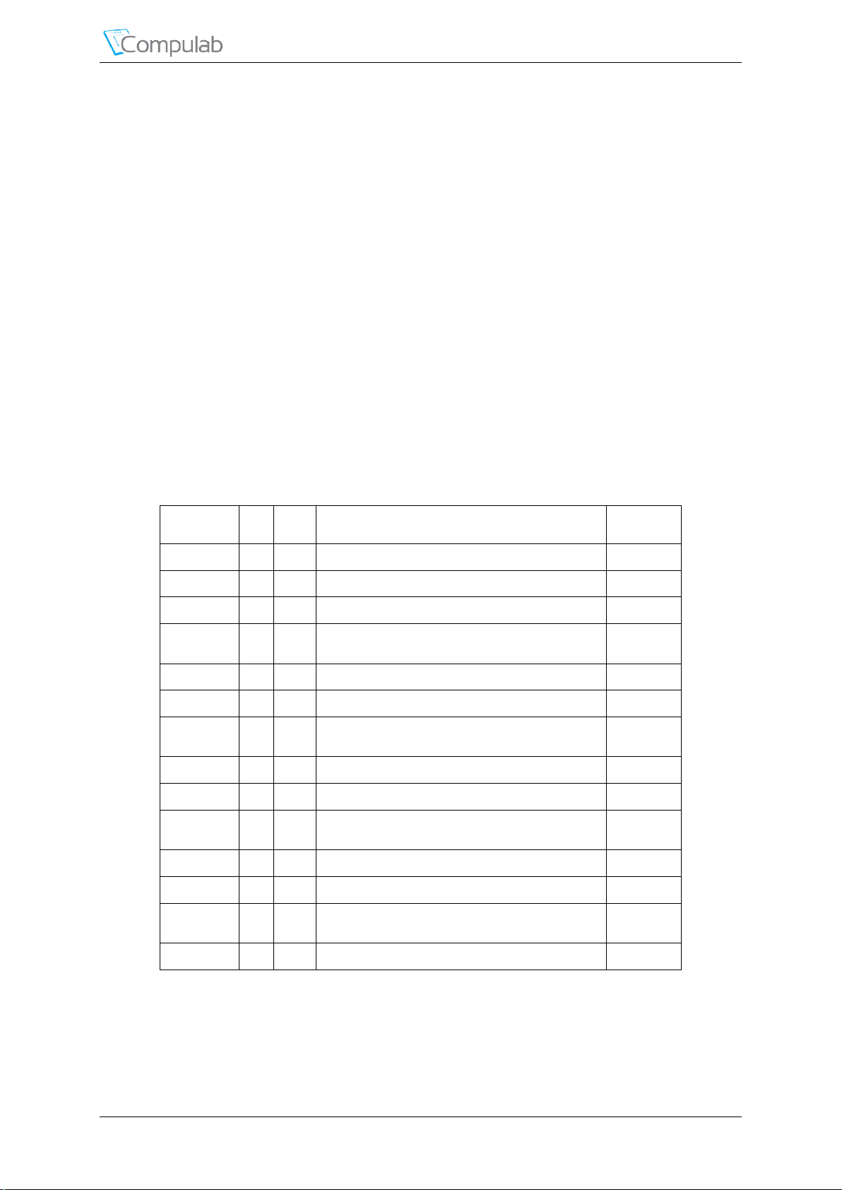
CL-SOM-AM57x PCI Express interface is derived from the AM57x integrated PCIe module.
Two instances of the PCIe are available. Two operation modes are supported with CL-SOMAM57x:
A single controller with two lanes (PCIe_SS1 only)
Two separate controllers with one lane each
Each PCI Express interface supports the following features:
Each PCIe subsystem controller has support for PCIe 2.0 mode (5.0 Gbps per lane) and 1.0
mode (2.5 Gbps per lane)
Supports either root complex (RC) or in end point (EP) PCIe mode
Complies with PCI local bus specification v3.0 and PCI express base standard v3.0
Support of EP legacy mode
Legacy PCI Interrupts reception (RC) and generation (EP)
Automatic Lane reversal as specified in the PCI Express standard 2.0 specification
(transmit and receive)
For additional details on PCI Express modules, please refer to the AM572x or AM571x technical
reference manual. The table below summarizes the PCIe interface signals
Table 14 PCIe Interface Signals
Revised April 2018 CL-SOM-AM57x 26
Page 27
Peripheral Interfaces
Signal Name
Pin #
Type
Description
Availability
SATA1_LED
181* O SATA channel activity indicator
Always
SATA1_LED
56* O SATA channel activity indicator
Always
SATA1_RXN0
29
IDS
SATA differential negative receiver lane 0
Always
SATA1_RXP0
27
IDS
SATA differential positive receiver lane 0
Always
SATA1_TXN0
23
ODS
SATA differential negative transmitter lane 0
Always
SATA1_TXP0
21
ODS
SATA differential positive transmitter lane 0
Always
Signal Name
Pin
#
Type
Description
Availability
USB_RXN0
184
IDS
USB1 USB3.0 receiver negative lane
Always
USB_RXP0
182
IDS
USB1 USB3.0 receiver positive lane
Always
USB_TXN0
190
ODS
USB1 USB3.0 transmitter negative lane
Always
USB_TXP0
188
ODS
USB1 USB3.0 transmitter positive lane
Always
USB1_DM
178
IODS
USB1 USB2.0 differential signal pair (negative)
Always
USB1_DP
176
IODS
USB1 USB2.0 differential signal pair (positive)
Always
USB1_DRVVBUS
200* O USB1 Drive VBUS signal
Always
USBOTG_ID
174* I USB1 USBOTG_ID signal
Always
4.4 SATA
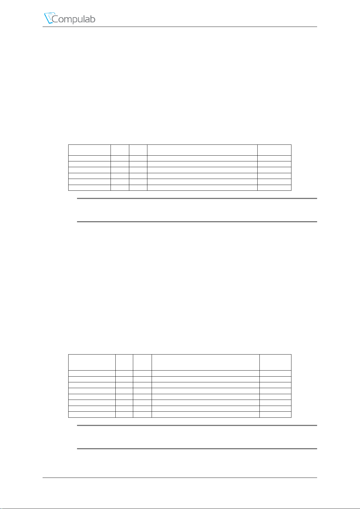
CL-SOM-AM57x incorporates one SATA-2 (3-Gbps) interface. The SATA controller supports
the following key features:
Serial ATA 1.5-Gbps and 3-Gbps speeds (SATA-1 and SATA-2)
Support of all SATA power management features
HBA port associated Internal DMA engine
Activity LED generation
For additional details on the SATA subsystem, please refer to the Sitara AM57x technical
reference manual. The table below summarizes the SATA interface signals
Table 15 SATA Interface Signals
NOTE: Pins denoted with "*" are multifunctional. For additional details please refer to
chapter 5.5 of this document
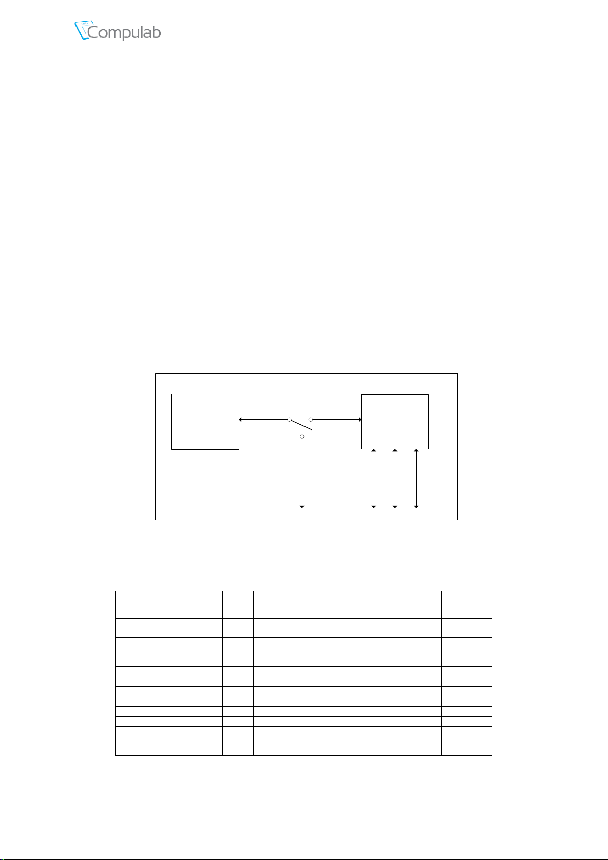
4.5 USB 3.0
USB3.0 interface is derived from the Sitara AM57x SuperSpeed (SS) USB 3.0 Dual-Role-Device
(DRD) subsystem. USB 3.0 DRD subsystem supports following features:
Integrated SS (USB3.0) PHY and HS/FS (USB2.0) PHY
Supports USB Peripheral (or Device) mode at speeds SS (5Gbps), HS, FS, and LS.
Supports USB Host mode at speeds SS (5Gbps), HS, FS, and LS.
USB static peripheral operation
USB static host operation
Flexible stream allocation
Stream priority
The table below summarizes the USB 3.0 interface signals
Table 16 USB 3.0 Interface Signals
NOTE: Pins denoted with "*" are multifunctional. For additional details please refer to
Revised April 2018 CL-SOM-AM57x 27
chapter 5.5 of this document
Page 28
Peripheral Interfaces
TI USB 2.0
port 2
Sitara AM57x
USB 2.0 DRD
subsystem
RGMII0
USB 2.0 HUB
HUB PORT 1
HUB PORT 2
HUB PORT 3
TI PORT 2
Hub Upstream
Signal Name
Pin
#
Type
Description
Availability
HUB_USB_OCN
162
I
Active LOW Overcurrent Condition Detection Input.
100K Pull Up onboard SOM-AM57x.
With "U4"
HUB_USB_PWREN
156
O
Power Switch Driver Output. 10KΩ Pull Up onboard
SOM-AM57x.
With "U4"
HUBUSB1_DN
170
IODS
Downstream Port 1 differential signal pair (negative)
With "U4"
HUBUSB1_DP
172
IODS
Downstream Port 1 differential signal pair (positive)
With "U4"
HUBUSB2_DN
164
IODS
Downstream Port 2 differential signal pair (negative)
With "U4"
HUBUSB2_DP
166
IODS
Downstream Port 2 differential signal pair (positive)
With "U4"
HUBUSB3_DN
158
IODS
Downstream Port 3 differential signal pair (negative)
With "U4"
HUBUSB3_DP
160
IODS
Downstream Port 3 differential signal pair (positive)
With "U4"
USB2_DM
170
IODS
USB2 USB2.0 differential signal pair (negative)
With "U2"
USB2_DP
172
IODS
USB2 USB2.0 differential signal pair (positive)
With "U2"
USB2_DRVVBUS
156
O
USB2 Drive VBUS signal. 10KΩ Pull Up onboard
SOM-AM57x.
With "U2"
4.6 USB2.0 ports
USB2.0 interface is derived from the Sitara AM57x High-Speed (HS) USB 2.0 Dual-Role-Device
(DRD) subsystem. USB 2.0 DRD subsystem supports following features:
Integrated HS/FS PHY
Supports USB Peripheral (or Device) mode at speeds HS(480 Mbps), FS, and LS.
Supports USB Host mode at speeds HS(480 Mbps), FS, and LS.
USB static peripheral operation
USB static host operation
In addition to the AM57x integrated USB2.0 DRD subsystem, the CL-SOM-AM57x is equipped
with a USB2.0 hub, providing three downstream host ports. The implementation of USB2.0 hub
precludes access to AM57x integrated USB2.0 DRD subsystem. The hub supports following
features:
Compliant with USB 2.0 specification
Three downstream ports
Downstream ports are backward compatible with FS, LS
For additional details on USB2.0 DRD subsystem of the Sitara AM57x, please refer to the
AM57x technical reference manual.
Figure 3 SOM-AM572x USB2.0 sub-system
Please refer to the AM57x Reference manual for additional details. The table below summarizes
the USB interface signals
Table 17 USB Interface Signals
Revised April 2018 CL-SOM-AM57x 28
Page 29
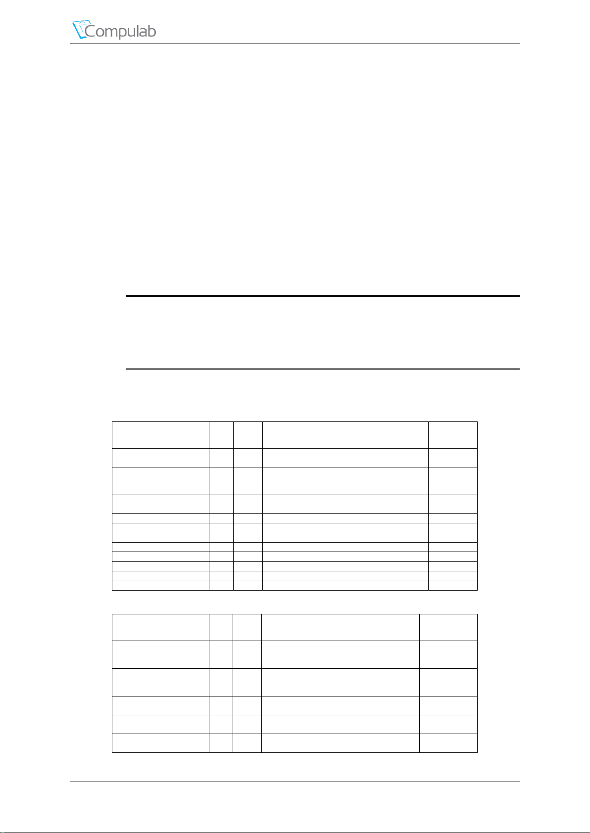
Peripheral Interfaces
Signal Name
Pin
#
Type
Description
Availability
ETH0_LED_ACT
107
IO
Active High, activity LED driver, fixed 2.5V
logic. 10KΩ Pull Down onboard SOM-AM57x
With "E2"
ETH0_LED_LINK10_100
97
IO
Active High, 10/100 link LED driver, fixed
2.5V logic. 10KΩ Pull Down onboard SOMAM57x
With "E2"
ETH0_LED_LINK1000
109
IO
Active High, 1Gbps link LED driver, fixed 2.5V
logic.
With "E2"
ETH0_MDI0N
83
AIO
Negative part of 100ohm diff-pair 0
With "E2"
ETH0_MDI0P
85
AIO
Positive part of 100ohm diff-pair 0
With "E2"
ETH0_MDI1N
77
AIO
Negative part of 100ohm diff-pair 1
With "E2"
ETH0_MDI1P
79
AIO
Positive part of 100ohm diff-pair 1
With "E2"
ETH0_MDI2N
89
AIO
Negative part of 100ohm diff-pair 2
With "E2"
ETH0_MDI2P
91
AIO
Positive part of 100ohm diff-pair 2
With "E2"
ETH0_MDI3N
101
AIO
Negative part of 100ohm diff-pair 3
With "E2"
ETH0_MDI3P
103
AIO
Positive part of 100ohm diff-pair 3
With "E2"
Signal Name
Pin
#
Type
Description
Availability
ETH1_LED_ACT
4
IO
Active High, activity LED driver, fixed 2.5V
logic. 10KΩ Pull Down onboard SOMAM57x
With "E1" OR
"E2"
ETH1_LED_LINK10_100
22
IO
Active High, 10/100 link LED driver, fixed
2.5V logic. 10KΩ Pull Down onboard SOMAM57x
With "E1" OR
"E2"
ETH1_LED_LINK1000
16
IO
Active High, 1Gbps link LED driver, fixed
2.5V logic.
With "E1" OR
"E2"
ETH1_MDI0N
6
AIO
Negative part of 100ohm diff-pair 0
With "E1" OR
"E2"
ETH1_MDI0P
8
AIO
Positive part of 100ohm diff-pair 0
With "E1" OR
"E2"
4.7 Ethernet
CL-SOM-AM57x incorporates two full-featured 10/100/1000 ethernet ports implemented with the
two MACs built into the AM57x SoC, coupled with two AR8033 RGMII Ethernet PHYs from
Atheros. Both ethernet interfaces support the following main features:
10/100/1000 BASE-T IEEE 802.3 compliant
Wire rate switching (802.1d)
Support for IEEE 1588 Clock Synchronization (2008 Annex D and Annex F) - inside the
MAC
Full duplex mode supported in 10/100/1000 Mbps. Half-duplex mode supported only in
10/100 Mbps
Automatic channel swap (ACS)
Automatic MDI/MDIX crossover
Automatic polarity correction
IEEE 802.3u compliant Auto-Negotiation
NOTE: CL-SOM-AM57x primary Ethernet port is available only with the ‘E2’ or ‘E1’
ordering options.
NOTE: CL-SOM-AM57x secondary Ethernet port is available only with ‘E2’ ordering
option.
Please refer to the AM57x and the Atheros AR8033 respective reference manuals for additional
details. The tables below summarize the Ethernet interface signals
Table 18 Ethernet0 Interface Signals
Table 19 Ethernet1 Interface Signals
Revised April 2018 CL-SOM-AM57x 29
Page 30
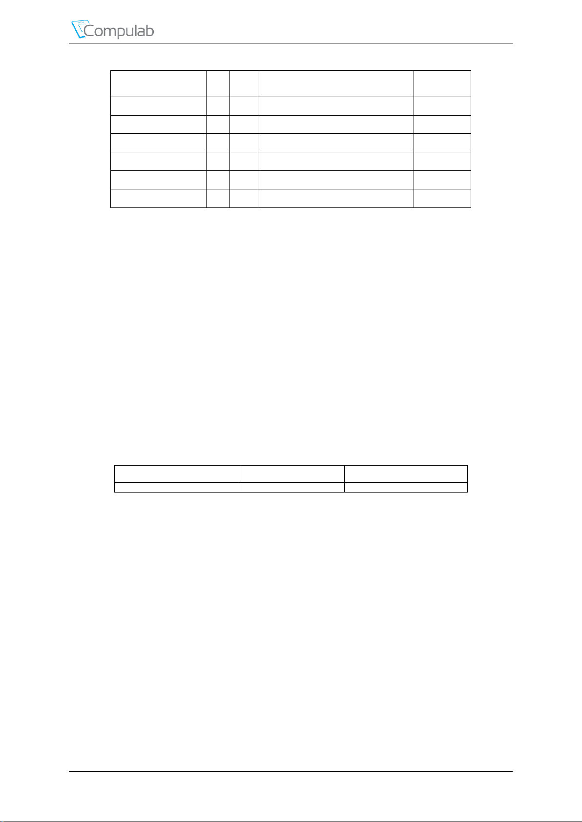
Peripheral Interfaces
Signal Name
Pin
#
Type
Description
Availability
ETH1_MDI1N
12
AIO
Negative part of 100ohm diff-pair 1
With "E1" OR
"E2"
ETH1_MDI1P
14
AIO
Positive part of 100ohm diff-pair 1
With "E1" OR
"E2"
ETH1_MDI2N
18
AIO
Negative part of 100ohm diff-pair 2
With "E1" OR
"E2"
ETH1_MDI2P
20
AIO
Positive part of 100ohm diff-pair 2
With "E1" OR
"E2"
ETH1_MDI3N
24
AIO
Negative part of 100ohm diff-pair 3
With "E1" OR
"E2"
ETH1_MDI3P
26
AIO
Positive part of 100ohm diff-pair 3
With "E1" OR
"E2"
Manufacturer
Mfg. P/N
Mating Connector
Hirose
U.FL-R-MT(10)
Hirose U.FL-LP-040
4.8 Wireless Interfaces
CL-SOM-AM57x optional wireless communication capabilities are implemented with one of the
following two assembly options:
2.4GHz WiFi only capability, Implemented with the “W” ordering option of CL-SOM-
AM57x. Please refer to WLAN Only section for additional details.
Dual-Band WiFi and Bluetooth capabilities, Implemented with the “WAB” ordering
option of CL-SOM-AM57x. Please refer to Dual Band WLAN & Bluetooth section for
additional details.
CL-SOM-AM57x is equipped with up-to two U.FL high frequency connectors allowing easy
integration with external antennas:
Primary WLAN/BT antenna connector J1. Can be used with any type of 2.4GHz/5.0GHz
antenna for WLAN & Bluetooth functionality. J1 is available with either “W” or “WAB”
ordering options of CL-SOM-AM57x.
Secondary WLAN antenna connector J2. Can be used with any type of 2.4GHz/5.0GHz
antenna for Dual-Band WLAN functionality. J2 is only available with the “WAB”
ordering option of CL-SOM-AM57x.
Table 20 J1 & J2 U.FL connector data
4.8.1 WLAN Only
CL-SOM-AM57x simple WLAN Only capabilities are based on the optional Texas Instruments
WL1801MOD WLAN module soldered onboard.
WL1801MOD is a WiLink™ 8 based Single-Band combo module enabling Wi-Fi® functionality
with CL-SOM-AM57x. WL1801MOD supports the following features:
FCC, IC, ETSI/CE, and TELEC modular certification.
Support of IEEE Std 802.11a, 802.11b, 802.11g and 802.11n.
20- and 40-MHz SISO and 20-MHz 2 x 2 MIMO at 2.4 GHz for High Throughput: 80
Mbps (TCP), 100 Mbps (UDP).
2.4-GHz MRC Support for Extended Range.
Wi-Fi Direct Concurrent Operation (Multichannel, Multirole).
When populated, WL1801MOD is interfaced with the AM57x through the following interfaces:
Revised April 2018 CL-SOM-AM57x 30
AM57x MMC/SD/SDIO2 interface is used for WLAN data.
Please refer to the AM57x and the Texas Instruments WL1801MOD respective reference manuals
for additional details.
Page 31
Peripheral Interfaces
Parameter
Test conditions
Min
Typ
Max
Unit
Stereo Headphone Output
0-dB full-scale output voltage
1.0 Vrms
Maximum output power, PO
R
load
= 32Ω
30 mW
NOTE: CL-SOM-AM57x WiFi 802.11 b/g/n (without Bluetooth) functionality is available
only with the ‘W’ ordering option.
4.8.2 Dual Band WLAN & Bluetooth
CL-SOM-AM57x can be optionally shipped with the Texas Instruments WL1837MOD
WLAN/Bluetooth module soldered onboard.
WL1837MOD is a WiLink™ 8 based Dual-Band industrial module enabling Wi-Fi®,
Bluetooth®, and Bluetooth Low Energy (BLE) functionality with CL-SOM-AM57x.
WL1837MOD supports the following features:
FCC, IC, ETSI/CE, and TELEC modular certification.
Support of IEEE Std 802.11a, 802.11b, 802.11g and 802.11n.
20- and 40-MHz SISO and 20-MHz 2 x 2 MIMO at 2.4 GHz for High Throughput: 80
Mbps (TCP), 100 Mbps (UDP).
2.4-GHz MRC Support for Extended Range and 5-GHz Diversity Capable.
Wi-Fi Direct Concurrent Operation (Multichannel, Multirole).
Bluetooth 4.1 Compliance and CSA2 Support.
Dedicated Audio Processor Support of SBC Encoding + A2DP.
Dual-Mode Bluetooth and BLE.
When populated, WL1837MOD is interfaced with the AM57x through the following interfaces:
AM57x MMC/SD/SDIO2 interface is used for WLAN data.
AM57x UART10 and McASP interfaces are employed for Bluetooth and A2DP data.
Please refer to the AM57x and the Texas Instruments WL1837MOD respective reference manuals
for additional details.
NOTE: CL-SOM-AM57x WiFi 802.11 a/b/g/n and Bluetooth functionality is available only
with the ‘WAB’ ordering option.
4.9 Analog Audio
The CL-SOM-AM57x analog audio functionality is implemented by interfacing the Wolfson
WM8731L audio codec with the AM57x McASP3 port. The WM8731L codec supports the
following main features:
Highly Efficient Headphone driver
Audio performance (‘A’ weighted): ADC SNR – 90dB, DAC SNR – 100dB.
Microphone input and electret bias with side tone mixer
ADC and DAC sampling frequency: 8kHz – 96kHz.
Selectable ADC high pass filter
NOTE: CL-SOM-AM57x Analog audio interface is available only with the ‘A’ ordering
option.
Revised April 2018 CL-SOM-AM57x 31
Table 21 Analog Audio Characteristics
Page 32
Peripheral Interfaces
Parameter
Test conditions
Min
Typ
Max
Unit
R
load
= 16Ω
50
Signal-to-noise ratio, Aweighted
90
97 dB
Total harmonic distortion
1kHz output,
Rload = 32Ω
P
out
= 10mW
rms (-5dB)
0.056
-65
0.1
60 % dB
P
out
= 20mW
rms (-2dB)
0.56
-45
1.0
40 % dB
Power supply rejection ratio
1 kHz, 100 mV
p-p
50
dB
20Hz – 20kHz, 100mV
p-p
45 Programmable gain
1 kHz output
-73 0 6
dB
Programmable-gain step size
1 kHz 1 dB
Mute attenuation
1 kHz output, 0dB
80 dB
Line Input to ADC
Input signal level (0 dB)
1.0 Vrms
Signal-to-noise ratio
A-weighted, 0dB gain,
Fsample = 48 kHz.
85
90
dB
A-weighted, 0dB gain,
Fsample = 96 kHz.
90 Dynamic range
A-weighted, −60-dB full-scale
input
85
90 dB
Total harmonic distortion
−1-dB input, 0-dB gain
-84
0.006
-74
0.02
dB
%
Power supply rejection ratio
1 kHz, 100 mV
p-p
50
dB
20Hz – 20kHz, 100mV
p-p
45
ADC Channel Separation
1 kHz input tone
90 dB
Programmable-gain
1 kHz input tone, Rsource<50Ω
-34.5 0 +12
dB
Programmable-gain step size
Guaranteed Monotonic
1.5 dB
Mute attenuation
0dB, 1 kHz input tone
80 dB
Input resistance
12 dB input gain
10
15
kΩ
0 dB input gain
20
30 Input capacitance
10 pF
Microphone Input to ADC
Input signal level (0 dB)
1.0 Vrms
Signal-to-noise ratio
A-weighted, 0-dB gain
85 dB
Dynamic range,
A-weighted, −60-dB full-scale
input
85 dB
Total harmonic distortion,
0dB input, 0dB gain
-60
-55
dB
Power supply rejection ratio
1 kHz, 100 mV
p-p
50
dB
20Hz – 20kHz, 100mV
p-p
45
Programmable-gain Boost
1kHz input, Rsource<50Ω,
MICBOOST bit is 1.
34 dB
Mic Path gain (MICBOOST
gain is additional to this
nominal gain)
MICBOOST bit is 0,
Rsource<50Ω,
14 dB
Mute attenuation
0dB, 1 kHz input tone
80 dB
Input resistance
10 kΩ
Input capacitance
10 pF
Microphone Bias
Bias voltage
2.37
5
2.475
2.57
5
V
Bias-current source
3 mA
Output noise voltage
1kHz to 20kHz
25 nV/√Hz
Signal Name
Pin #
Type
Description
Availability
LHPOUT
203
AO
Left Channel Headphone Output
With "A"
LLINEIN
199
AI
Left channel line input
With "A"
MICBIAS
191
AP
Electret microphone bias supply
With "A"
MICIN
193
AI
Microphone input
With "A"
RHPOUT
201
AO
Right Channel Headphone Output
With "A"
RLINEIN
197
AI
Right channel line input
With "A"
Revised April 2018 CL-SOM-AM57x 32
Please refer to the Wolfson Microelectronics WM8731L datasheet for additional details. The table
below summarizes the analog audio interface signals
Table 22 analog audio Interface Signals
Page 33
Peripheral Interfaces
Signal Name
Pin
#
Type
Description
Availability
MCASP2_ACLKX
137*
IO
MCASP2 Transmit Bit Clock I/O
Always
MCASP2_AHCLKX
154*
O
MCASP2 Transmit High-Frequency Master Clock
I/O
Always
MCASP2_AXR0
139
IO
MCASP2 Transmit/Receive Data I/O
Always
MCASP2_AXR1
143
IO
MCASP2 Transmit/Receive Data I/O
Always
MCASP2_FSX
145*
IO
MCASP2 Transmit Frame Sync I/O
Always
Signal Name
Pin
#
Type
Description
Availability
MCASP3_ACLKR
199*
IO
MCASP3 Receive Bit Clock I/O
Without
"A"
MCASP3_ACLKX
199*
IO
MCASP3 Transmit Bit Clock I/O
Without
"A"
MCASP3_AHCLKX
193*
O
MCASP3 Transmit High-Frequency Master Clock
I/O
Without
"A"
MCASP3_AXR0
201*
IO
MCASP2 Transmit/Receive Data I/O
Without
"A"
MCASP3_AXR1
197*
IO
MCASP2 Transmit/Receive Data I/O
Without
"A"
MCASP3_FSR
203*
IO
MCASP3 Receive Frame Sync I/O
Without
"A"
MCASP3_FSX
203*
IO
MCASP3 Transmit Frame Sync I/O
Without
"A"
Signal Name
Pin
#
Type
Description
Availability
MCASP4_ACLKR
13*
IO
MCASP4 Receive Bit Clock I/O
Always
MCASP4_ACLKX
13*
IO
MCASP4 Transmit Bit Clock I/O
Always
MCASP4_AHCLKX
97*
O
MCASP4 Transmit High-Frequency Master Clock
I/O
Without
"E2"
MCASP4_AXR0
15*
IO
MCASP4 Transmit/Receive Data I/O
Always
MCASP4_AXR1
17*
IO
MCASP4 Transmit/Receive Data I/O
Always
MCASP4_FSR
11*
IO
MCASP4 Receive Frame Sync I/O
Always
MCASP4_FSX
11*
IO
MCASP4 Transmit Frame Sync I/O
Always
4.10 Digital Audio (McASP)
The multichannel digital audio interface available with CL-SOM-AM57x is based on the
multichannel audio serial port module integrated into Sitara AM57x SoC. Up to four instances of
the McASP block are available with CL-SOM-AM57x. McASP supports the following main
features:
S/PDIF, IEC60958-1, AES-3 formats
Wide variety of I2S and similar bit-stream format
S/PDIF, IEC60958-1, AES-3 formats - Transmit section only.
TDM stream of 384 time slots specifically designed for easy interface to external digital
interface receiver (DIR) device transmitting DIR frames to MCASP using the I2S protocol
(one time slot for each DIR subframe) - Receive section.
Programmable clock and frame sync polarity (rising or falling edge): ACLKR/X,
AHCLKR/X, and AFSR/X.
Slot length (number of bits per time slot): 8, 12, 16, 20, 24, 28, 32 bits supported.
Word length (bits per word): 8, 12, 16, 20, 24, 28, 32 bits; always less than or equal to the
time slot length.
For additional details on McASP, please refer to the Sitara AM57x technical reference manual.
The tables below summarize the McASP interface signals
Table 23 McASP2 Interface Signals
Table 24 McASP3 Interface Signals
Table 25 McASP4 Interface Signals
Revised April 2018 CL-SOM-AM57x 33
Page 34
Peripheral Interfaces
Signal Name
Pin
#
Type
Description
Availability
MCASP5_ACLKR
5*
IO
MCASP5 Receive Bit Clock I/O
Always
MCASP5_ACLKX
5*
IO
MCASP5 Transmit Bit Clock I/O
Always
MCASP5_AHCLKX
152*
O
MCASP5 Transmit High-Frequency Master Clock
I/O
Always
MCASP5_AXR0
7*
IO
MCASP5 Transmit/Receive Data I/O
Always
MCASP5_AXR1
9*
IO
MCASP5 Transmit/Receive Data I/O
Always
MCASP5_FSR
3*
IO
MCASP5 Receive Frame Sync I/O
Always
MCASP5_FSX
3*
IO
MCASP5 Transmit Frame Sync I/O
Always
Signal Name
Pin #
Type
Description
Availability
MMC1_CLK
80*
IO
MMC1 clock
Always
MMC1_CMD
82*
IO
MMC1 command
Always
MMC1_DAT0
84*
IO
MMC1 data bit 0
Always
MMC1_DAT1
86*
IO
MMC1 data bit 1
Always
Table 26 McASP5 Interface Signals
NOTE: Pins denoted with "*" are multifunctional. For additional details please refer to
chapter 5.5 of this document
4.11 MMC / SD /SDIO
Up to three full featured eMMC/SD/SDIO ports are available with CL-SOM-AM57x. The ports
are implemented with three instances of the eMMC/SD/SDIO host controller integrated into the
Sitara AM57x SoC. The eMMC/SD/SDIOi controller is also referred to as MMCi. The following
general features are supported:
Full compliance with MMC/eMMC command/response sets as defined in the JC64
MMC/eMMC standard specification, v4.5
Full compliance with SD command/response sets as defined in the SD Physical Layer
specification v3.01
Full compliance with SDIO command/response sets and interrupt/read-wait suspend-
resume operations as defined in the SD part E1 specification v3.00
Full compliance with SD Host Controller Standard Specification sets as defined in the SD
card specification Part A2 v3.00
Built-in 1024-byte buffer for read or write
Supported SD v3.0 data transfer rates:
DS mode (3.3V IOs): up to 12 MBps (24 MHz clock)
HS mode (3.3V IOs): up to 24 MBps (48 MHz clock)
Each controller has the following features:
MMC1 - 4-bit wide data bus, supports 1- and 4-bit data transfers (mainly used for
connection with SD cards).
MMC3 - 8-bit wide data bus, supports 1-, 4-, and 8-bit data transfers (mainly used for
connection with SDIO cards).
MMC4 - 4-bit wide data bus, supports 1- and 4-bit data transfers (mainly used for
connection with SDIO cards).
NOTE: CL-SOM-AM57x MMC/SD/SDIO port 4 is available only without the ‘W’ and
Please refer to the AM57x Reference manual for additional details. The tables below summarize
the MMC/SD/SDIO interface signals
Table 27 MMC/SD/SDIO 1 Interface Signals
Revised April 2018 CL-SOM-AM57x 34
‘WAB’ ordering options.
Page 35
Peripheral Interfaces
Signal Name
Pin #
Type
Description
Availability
MMC1_DAT2
88*
IO
MMC1 data bit 2
Always
MMC1_DAT3
90*
IO
MMC1 data bit 3
Always
MMC1_SDCD
61*
I
MMC1 Card Detect
Always
MMC1_SDWP
67*
I
MMC1 Write Protect
Always
Signal Name
Pin #
Type
Description
Availability
MMC3_CLK
75*
IO
MMC3 clock
Always
MMC3_CMD
69*
IO
MMC3 command
Always
MMC3_DAT0
63*
IO
MMC3 data bit 0
Always
MMC3_DAT1
65*
IO
MMC3 data bit 1
Always
MMC3_DAT2
58*
IO
MMC3 data bit 2
Always
MMC3_DAT3
52*
IO
MMC3 data bit 3
Always
MMC3_DAT4
202*
IO
MMC3 data bit 4
Always
MMC3_DAT5
163*
IO
MMC3 data bit 5
Always
MMC3_DAT6
194*
IO
MMC3 data bit 6
Always
MMC3_DAT7
179*
IO
MMC3 data bit 7
Always
MMC3_SDCD
40*
I
MMC3 Card Detect
Always
MMC3_SDWP
34*
I
MMC3 Write Protect
Always
Signal Name
Pin #
Type
Description
Availability
MMC4_CLK
157*
IO
MMC4 clock
Without "W"/ "WAB"
MMC4_CMD
147*
IO
MMC4 command
Without "W"/ "WAB"
MMC4_DAT0
155*
IO
MMC4 data bit 0
Without "W"/ "WAB"
MMC4_DAT1
153*
IO
MMC4 data bit 1
Without "W"/ "WAB"
MMC4_DAT2
151*
IO
MMC4 data bit 2
Without "W"/ "WAB"
MMC4_DAT3
149*
IO
MMC4 data bit 3
Without "W"/ "WAB"
MMC4_SDCD
60*
I
MMC4 Card Detect
Always
MMC4_SDWP
62*
I
MMC4 Card Detect
Always
Signal Name
Pin
#
Type
Description
Availability
UART1_CTSN
157* I UART1 clear to send active low
Without "W"/ "WAB"
UART1_DCDN
155* I UART1 Data Carrier Detect active low
Without "W"/ "WAB"
UART1_DSRN
153* I UART1 Data Set Ready Active Low
Without "W"/ "WAB"
UART1_DTRN
151* O UART1 Data Terminal Ready Active Low
Without "W"/ "WAB"
Table 28 MMC/SD/SDIO 3 Interface Signals
Table 29 MMC/SD/SDIO 4 Interface Signals
NOTE: Pins denoted with "*" are multifunctional. For additional details please refer to
4.12 UART
CL-SOM-AM57x provides up to 9 UART ports. The functionality is derived from the UART
modules integrated into the Sitara AM5 7x SoC. One UART port supports IrDA features. The
following general features are supported:
16C750 compatibility
Baud rate from 300 bps up to 12 Mbps
Flow control: Hardware (RTS/CTS) or software (XON/XOFF)
UART1 module has extended modem control signals (DCD, RI, DTR, DSR)
Support of IrDA 1.4 slow infrared (SIR), medium infrared (MIR), and fast infrared (FIR)
communications (UART3 only).
Support of consumer infrared (CIR) for remote control applications (UART3 only)
For additional details on UART, please refer to the Sitara AM57x technical reference manual. The
tables below summarize the UART interface signals
Table 30 UART1 Interface Signals
chapter 5.5 of this document
Revised April 2018 CL-SOM-AM57x 35
Page 36
Peripheral Interfaces
Signal Name
Pin
#
Type
Description
Availability
UART1_RIN
149* I UART1 Ring Indicator Input
Without "W"/ "WAB"
UART1_RTSN
147* O UART1 request to send active low
Without "W"/ "WAB"
UART1_RXD
60* I UART1 Receive Data Input
Always
UART1_TXD
62* O UART1 Transmit Data Output
Always
Signal Name
Pin #
Type
Description
Availability
UART2_CTSN
151* I UART2 clear to send active low
Without "W"/ "WAB"
UART2_RTSN
149* O UART2 request to send active low
Without "W"/ "WAB"
UART2_RXD
155* I UART2 Receive Data Input
Without "W"/ "WAB"
UART2_TXD
153* O UART2 Transmit Data Output
Without "W"/ "WAB"
Signal Name
Pin
#
Type
Description
Availability
UART3_CTSN
155* I UART3 clear to send active low
Without "W"/
"WAB"
UART3_IRTX
149* O Infrared data output
Without "W"/
"WAB"
UART3_RCTX
155* O Remote control data output
Without "W"/
"WAB"
UART3_RTSN
153* O UART3 request to send active low
Without "W"/
"WAB"
UART3_RXD
117*
I
UART3 Receive Data Input for both normal UART
mode and IrDA mode.
Always
UART3_RXD
7*
I
UART3 Receive Data Input for both normal UART
mode and IrDA mode.
Always
UART3_RXD
151*
I
UART3 Receive Data Input for both normal UART
mode and IrDA mode.
Without "W"/
"WAB"
UART3_SD
153* O Infrared transceiver configure/shutdown
Without "W"/
"WAB"
UART3_TXD
111* O UART3 Transmit Data Output
Always
UART3_TXD
9* O UART3 Transmit Data Output
Always
UART3_TXD
149* O UART3 Transmit Data Output
Without "W"/
"WAB"
Signal Name
Pin #
Type
Description
Availability
UART4_RXD
15*
I
UART4 Receive Data Input.
Always
UART4_RXD
40*
I
UART4 Receive Data Input.
Always
UART4_TXD
17*
O
UART4 Transmit Data Output
Always
UART4_TXD
34*
O
UART4 Transmit Data Output
Always
Signal Name
Pin #
Type
Description
Availability
UART5_CTSN
89* I UART5 clear to send active low
Without "E2"
UART5_CTSN
58* I UART5 clear to send active low
Always
UART5_RTSN
91* O UART5 request to send active low
Without "E2"
UART5_RTSN
52* O UART5 request to send active low
Always
UART5_RXD
101*
I
UART5 Receive Data Input
Without "E2"
UART5_RXD
106*
I
UART5 Receive Data Input
Always
UART5_RXD
201*
I
UART5 Receive Data Input
Without "A"
UART5_RXD
63* I UART5 Receive Data Input
Always
UART5_TXD
103*
O
UART5 Transmit Data Output
Without "E2"
UART5_TXD
108*
O
UART5 Transmit Data Output
Always
UART5_TXD
197*
O
UART5 Transmit Data Output
Without "A"
UART5_TXD
65* O UART5 Transmit Data Output
Always
Signal Name
Pin #
Type
Description
Availability
UART6_CTSN
83* I UART6 clear to send active low
Without "E2"
UART6_RTSN
85* O UART6 request to send active low
Without "E2"
UART6_RXD
77* I UART6 Receive Data Input
Without "E2"
Table 31 UART2 Interface Signals
Table 32 UART3 Interface Signals
Table 33 UART4 Interface Signals
Table 34 UART5 Interface Signals
Table 35 UART6 Interface Signals
Revised April 2018 CL-SOM-AM57x 36
Page 37
Peripheral Interfaces
Signal Name
Pin #
Type
Description
Availability
UART6_RXD
124*
I
UART6 Receive Data Input
Always
UART6_RXD
135*
I
UART6 Receive Data Input
Always
UART6_RXD
61* I UART6 Receive Data Input
Always
UART6_TXD
79* O UART6 Transmit Data Output
Without "E2"
UART6_TXD
126*
O
UART6 Transmit Data Output
Always
UART6_TXD
129*
O
UART6 Transmit Data Output
Always
UART6_TXD
67* O UART6 Transmit Data Output
Always
Signal Name
Pin #
Type
Description
Availability
UART7_CTSN
201*
I
UART7 clear to send active low
Without "A"
UART7_RTSN
197*
O
UART7 request to send active low
Without "A"
UART7_RXD
89* I UART7 Receive Data Input
Without "E2"
UART7_RXD
94* I UART7 Receive Data Input
Always
UART7_RXD
199*
I
UART7 Receive Data Input
Without "A"
UART7_TXD
91* O UART7 Transmit Data Output
Without "E2"
UART7_TXD
92* O UART7 Transmit Data Output
Always
UART7_TXD
203*
O
UART7 Transmit Data Output
Without "A"
Signal Name
Pin #
Type
Description
Availability
UART8_CTSN
15* I UART8 clear to send active low
Always
UART8_RTSN
17* O UART8 request to send active low
Always
UART8_RXD
13* I UART8 Receive Data Input
Always
UART8_RXD
83* I UART8 Receive Data Input
Without "E2"
UART8_RXD
54* I UART8 Receive Data Input
Always
UART8_TXD
11* O UART8 Transmit Data Output
Always
UART8_TXD
85* O UART8 Transmit Data Output
Without "E2"
UART8_TXD
56* O UART8 Transmit Data Output
Always
Signal Name
Pin #
Type
Description
Availability
UART9_CTSN
7* I UART9 clear to send active low
Always
UART9_RTSN
9* O UART9 request to send active low
Always
UART9_RXD
5* I UART9 Receive Data Input
Always
UART9_RXD
157*
I
UART9 Receive Data Input
Without "W"/
"WAB"
UART9_TXD
3* O UART9 Transmit Data Output
Always
UART9_TXD
73* O UART9 Transmit Data Output
Always
UART9_TXD
147*
O
UART9 Transmit Data Output
Without "W"/
"WAB"
Signal Name
Pin #
Type
Description
Availability
UART10_CTSN
194*
I
UART10 clear to send active low
Without "W"/ "WAB"
UART10_RTSN
179*
O
UART10 request to send active low
Without "W"/ "WAB"
UART10_RXD
115*
I
UART10 Receive Data Input
Without "W"/ "WAB"
UART10_RXD
202*
I
UART10 Receive Data Input
Without "W"/ "WAB"
UART10_RXD
151*
I
UART10 Receive Data Input
Without "W"/ "WAB"
UART10_TXD
113*
O
UART10 Transmit Data Output
Without "W"/ "WAB"
UART10_TXD
163*
O
UART10 Transmit Data Output
Without "W"/ "WAB"
UART10_TXD
149*
O
UART10 Transmit Data Output
Without "W"/ "WAB"
Table 36 UART7 Interface Signals
Table 37 UART8 Interface Signals
Table 38 UART9 Interface Signals
Table 39 UART10 Interface Signals
NOTE: Pins denoted with "*" are multifunctional. For additional details please refer to
chapter 5.5 of this document
Revised April 2018 CL-SOM-AM57x 37
Page 38
4.13 SPI
Signal
Name
Pin
#
Type
Description
Availability
SPI1_CS0
72*
I/O
SPI1 Chip Select I/O
Without "I"
SPI1_CS1
181*
I/O
SPI1 Chip Select I/O
Always
SPI1_CS2
40*
I/O
SPI1 Chip Select I/O
Always
SPI1_CS3
34*
I/O
SPI1 Chip Select I/O
Always
SPI1_D0
66*
I/O
SPI1 Data I/O. Can be configured as either MISO or MOSI.
Without "I"
SPI1_D1
68*
I/O
SPI1 Data I/O. Can be configured as either MISO or MOSI.
Without "I"
SPI1_SCLK
70*
I/O
SPI1 Clock I/O
Without "I"
Signal
Name
Pin
#
Type
Description
Availability
SPI3_CS0
98*
I/O
SPI3 Chip Select I/O
Always
SPI3_CS0
58*
I/O
SPI3 Chip Select I/O
Always
SPI3_CS0
17*
I/O
SPI3 Chip Select I/O
Always
SPI3_CS1
161*
I/O
SPI3 Chip Select I/O
Always
SPI3_CS1
52*
I/O
SPI3 Chip Select I/O
Always
SPI3_CS2
106*
I/O
SPI3 Chip Select I/O
Always
SPI3_CS3
76*
I/O
SPI3 Chip Select I/O
Always
SPI3_D0
100*
I/O
SPI3 Data I/O. Can be configured as either MISO or MOSI.
Always
SPI3_D0
65*
I/O
SPI3 Data I/O. Can be configured as either MISO or MOSI.
Always
SPI3_D0
15*
I/O
SPI3 Data I/O. Can be configured as either MISO or MOSI.
Always
SPI3_D1
111*
I/O
SPI3 Data I/O. Can be configured as either MISO or MOSI.
Always
SPI3_D1
104*
I/O
SPI3 Data I/O. Can be configured as either MISO or MOSI.
Always
SPI3_D1
63*
I/O
SPI3 Data I/O. Can be configured as either MISO or MOSI.
Always
SPI3_D1
11*
I/O
SPI3 Data I/O. Can be configured as either MISO or MOSI.
Always
SPI3_SCLK
117*
I/O
SPI3 Clock I/O
Always
SPI3_SCLK
102*
I/O
SPI3 Clock I/O
Always
SPI3_SCLK
69*
I/O
SPI3 Clock I/O
Always
SPI3_SCLK
13*
I/O
SPI3 Clock I/O
Always
Signal
Name
Pin
#
Type
Description
Availability
SPI4_CS0
9*
I/O
SPI4 Chip Select I/O
Always
SPI4_CS0
179*
I/O
SPI4 Chip Select I/O
Always
SPI4_CS1
95*
I/O
SPI4 Chip Select I/O
Always
SPI4_CS2
111*
I/O
SPI4 Chip Select I/O
Always
SPI4_CS3
81*
I/O
SPI4 Chip Select I/O
Always
SPI4_D0
7*
I/O
SPI4 Data I/O. Can be configured as either MISO or MOSI.
Always
SPI4_D0
194*
I/O
SPI4 Data I/O. Can be configured as either MISO or MOSI.
Always
SPI4_D1
73*
I/O
SPI4 Data I/O. Can be configured as either MISO or MOSI.
Always
SPI4_D1
3*
I/O
SPI4 Data I/O. Can be configured as either MISO or MOSI.
Always
SPI4_D1
163*
I/O
SPI4 Data I/O. Can be configured as either MISO or MOSI.
Always
SPI4_SCLK
5*
I/O
SPI4 Clock I/O
Always
SPI4_SCLK
202*
I/O
SPI4 Clock I/O
Always
Up-to three SPI interfaces are accessible through the CL-SOM-AM57x carrier board interface.
The SPI interfaces are derived from AM57x integrated multichannel serial port interface (McSPI).
Each instance of McSPI port can operate as either a master or as an SPI slave. The following
features are supported:
Serial clock with programmable frequency, polarity, and phase for each channel.
Wide selection of SPI word lengths, ranging from 4 to 32 bits.
Up to four master channels, or single channel in slave mode.
Master multichannel mode: Full duplex/half duplex.
For additional details on McSPI, please refer to the Sitara AM57x technical reference manual. The
tables below summarize the SPI interface signals
Table 40 SPI1 Interface Signals
Peripheral Interfaces
Table 41 SPI3 Interface Signals
Table 42 SPI4 Interface Signals
Revised April 2018 CL-SOM-AM57x 38
Page 39
NOTE: Pins denoted with "*" are multifunctional. For additional details please refer to
Signal Name
Pin #
Type
Description
Availability
I2C2_SDA
25*
IOD
I2C2 Data I/O
Always
I2C2_SCL
31*
IOD
I2C2 Clock I/O
Always
Signal Name
Pin #
Type
Description
Availability
I2C3_SCL
43*
IOD
I2C2 Clock I/O
Always
I2C3_SCL
113*
IOD
I2C2 Clock I/O
Always
I2C3_SDA
49*
IOD
I2C2 Data I/O
Always
I2C3_SDA
115*
IOD
I2C2 Data I/O
Always
Signal Name
Pin #
Type
Description
Availability
I2C5_SCL
129*
IOD
I2C2 Clock I/O
Always
I2C5_SCL
3*
IOD
I2C2 Clock I/O
Always
I2C5_SCL
77*
IOD
I2C2 Clock I/O
Without "E2"
I2C5_SDA
135*
IOD
I2C2 Data I/O
Always
I2C5_SDA
5*
IOD
I2C2 Data I/O
Always
I2C5_SDA
79*
IOD
I2C2 Data I/O
Without "E2"
4.14 I2C
CL-SOM-AM57x is equipped with three I2C bus interfaces: I2C2, I2C3, and I2C5. The I2C
interfaces are derived from Sitara AM57x I2C controllers. I2C2 controller support Fast mode (up
to 400Kbps). I2C3 and I2C5 controller support HS mode (up to 3.4Mbps). The following general
features are supported by all I2C bus interfaces:
Compliant with Philips I2C specification version 2.1
Supports a standard mode (up to 100 kbps) and fast mode (up to 400 kbps)
Supports HS mode for transfer up to 3.4 Mbps (only for I2C3 and I2C5)
7-bit and 10-bit device addressing modes
Multimaster transmitter/receiver modes (master or slave)
NOTE: I2C1 and I2C4 are used on CL-SOM-AM57x and not accessible on the interface
Peripheral Interfaces
chapter 5.5 of this document
connector.
For additional details on I2C, please refer to the Sitara AM57x technical reference manual. The
tables below summarize the I2C interface signals
Table 43 I2C2 Interface Signals
Table 44 I2C3 Interface Signals
Table 45 I2C5 Interface Signals
NOTE: Pins denoted with "*" are multifunctional. For additional details please refer to
chapter 5.5 of this document
4.15 CAN Bus
CL-SOM-AM57x is equipped with two instances of the CAN bus controller. Each interface is
implemented with the AM57x integrated DCAN module. The following features are supported by
the DCAN module:
Supports CAN protocol version 2.0 part A, B
Bit rates up to 1 MBit/s
Revised April 2018 CL-SOM-AM57x 39
Page 40
Peripheral Interfaces
Signal Name
Pin #
Type
Description
Availability
DCAN1_RX
56*
I/O
DCAN1 receive data pin
Always
DCAN1_TX
54*
I/O
DCAN1 transmit data pin
Always
Signal Name
Pin #
Type
Description
Availability
DCAN2_RX
113*
I/O
DCAN2 receive data pin
Always
DCAN2_RX
34*
I/O
DCAN2 receive data pin
Always
DCAN2_TX
115*
I/O
DCAN2 transmit data pin
Always
DCAN2_TX
40*
I/O
DCAN2 transmit data pin
Always
Signal Name
Pin #
Type
Description
Availability
TS_XN
68
AIO
Touch screen X- (left)
With "I"
TS_XP
66
AIO
Touch screen X+ (right)
With "I"
TS_YN
72
AIO
Touch screen Y- (bottom)
With "I"
TS_YP
70
AIO
Touch screen Y+ (top)
With "I"
64 message objects in a dedicated message RAM
Support for DMA access
For additional details on DCAN, please refer to the Sitara AM57x technical reference manual.
The tables below summarize the CAN interface signals
Table 46 CAN1 Interface Signals
Table 47 CAN2 Interface Signals
NOTE: Pins denoted with "*" are multifunctional. For additional details please refer to
chapter 5.5 of this document
4.16 Resistive Touch Interface
CL-SOM-AM57x features an optional on-board Texas Instruments TSC2046 resistive touchscreen controller. The controller is communicating with the AM57x SoC over the QSPI interface.
The interface supports 4-wire touch panels and is available through the CL-SOM-AM57x carrier
board interface.
NOTE: CL-SOM-AM57x Resistive touch interface is available only with the ‘I’ ordering
option.
Please refer to Texas Instruments TSC2046 datasheet for additional details. The table below
summarizes the resistive touch interface signals
Table 48 resistive touch Interface Signals
4.17 HDQ / 1-Wire
CL-SOM-AM57x features a single instance of the HDQ/1-Wire interface. The interface is derived
from the HDQ1W module integrated into the Sitara AM57x SoC. HDQ1W supports the following
features:
Revised April 2018 CL-SOM-AM57x 40
Software selectable HDQ or 1-Wire mode
Benchmarq HDQ protocol
Dallas Semiconductor 1-Wire protocol
Power-down mode
For additional details on HDQ1W, please refer to the Sitara AM57x technical reference manual.
The table below summarizes the HDQ/1-wire interface signals
Page 41
Peripheral Interfaces
Signal Name
Pin #
Type
Description
Availability
HDQ0
152*
IOD
HDQ or 1-wire protocol single interface pin
Always
HDQ0
97*
IOD
HDQ or 1-wire protocol single interface pin
Without "E2"
Signal Name
Pin #
Type
Description
Availability
EHRPWM1A
73* O EHRPWM1 Output A
Always
EHRPWM2_TRIPZONE_INPUT
75*
IO
EHRPWM2 Trip Zone Input
Always
EHRPWM2A
49* O EHRPWM2 Output A
Always
EHRPWM2B
43* O EHRPWM2 Output B
Always
EHRPWM3_TRIPZONE_INPUT
194*
IO
EHRPWM3 Trip Zone Input
Always
EHRPWM3A
202* O EHRPWM3 Output A
Always
EHRPWM3B
163* O EHRPWM3 Output B
Always
Table 49 HDQ/1-wire Interface Signals
NOTE: Pins denoted with "*" are multifunctional. For additional details please refer to
chapter 5.5 of this document
4.18 Enhanced High Resolution PWM module (eHRPWM)
Three enhanced high resolution pulse width modulator (eHRPWM) module instances are
accessible through the CL-SOM-AM57x carrier board interface. All eHRPWM modules are
derived from the Sitara AM57x on-SoC. Each eHRPWM module supports the following features:
Dedicated 16 bit time-base with Period / Frequency control
Two PWM outputs (EHRPWMA and EHRPWMB) that can be used in the following
configurations:
Two independent PWM outputs with single-edge operation
Two independent PWM outputs with dual-edge symmetric operation
One independent PWM output with dual-edge asymmetric operation
Supports Dead-band generation with independent Rising and Falling edge delay control
Provides asynchronous over-ride control of PWM signals during fault conditions
Supports “trip zone” allocation of both latched and un-latched fault conditions
Allows events to trigger both CPU interrupts and start of ADC conversions
Support PWM chopping by high frequency carrier signal, used for pulse transformer gate
drives.
For additional details on eHRPWM, please refer to the Sitara AM57x technical reference manual.
The table below summarizes the eHRPWM interface signals
Table 50 eHRPWM Interface Signals
NOTE: Pins denoted with "*" are multifunctional. For additional details please refer to
chapter 5.5 of this document
4.19 Enhanced Capture module (eCAP)
Two enhanced capture (eCAP) module instances are accessible through the CL-SOM-AM57x
carrier board interface. All eCAP modules are derived from the Sitara AM57x on-SoC. eCAP can
be used for the following applications:
Sample rate measurements of audio inputs
Speed measurements of rotating machinery (for example, toothed sprockets sensed via Hall
sensors)
The following features are supported with eCAP:
Revised April 2018 CL-SOM-AM57x 41
Page 42
Peripheral Interfaces
Signal Name
Pin #
Type
Description
Availability
ECAP2_IN_PWM2_OUT
69*
IO
ECAP2 Capture Iniput / PWM Output
Always
ECAP3_IN_PWM3_OUT
179*
IO
ECAP3 Capture Iniput / PWM Output
Always
Signal Name
Pin #
Type
Description
Availability
EQEP3_INDEX
58*
IO
EQEP3 Index Input
Always
EQEP3_STROBE
52*
IO
EQEP3 Strobe Input
Always
Signal Name
Pin #
Type
Description
Availability
PR2_MDIO_DATA
9*
IO
MDIO Data
Always
PR2_MDIO_DATA
9*
IO
MDIO Data
Always
PR2_MDIO_MDCLK
7* O MDIO Clock
Always
PR2_MDIO_MDCLK
7* O MDIO Clock
Always
32-bit time base counter
4-event time-stamp registers (each 32 bits)
Edge polarity selection for up to four sequenced time-stamp capture events
Interrupt on either of the four events
Single shot capture of up to four event time-stamps
Continuous mode capture of time-stamps in a four-deep circular buffer
When not used in capture mode, the ECAP module can be configured as a single channel
PWM output
For additional details on eCAP, please refer to the Sitara AM57x technical reference manual. The
table below summarizes the eCAP interface signals
Table 51 eCAP Interface Signals
NOTE: Pins denoted with "*" are multifunctional. For additional details please refer to
chapter 5.5 of this document
4.20 Quadrature Encoder Pulse module (eQEP)
One enhanced quadrature encoder pulse (eQEP3) module instance is accessible through the CLSOM-AM57x carrier board interface. eQEP3 module is derived from the Sitara AM57x on-SoC.
The eQEP3 module allows effective sensing of wheel rotation parameters such as direction and
speed without software intervention. The eQEP3 inputs include two pins for quadrature-clock
mode or direction-count mode, an index (or 0 marker), and a strobe input.
For additional details on eQEP3, please refer to the Sitara AM57x technical reference manual.
The table below summarizes the eQEP3 interface signals
Table 52 eQEP3 Interface Signals
NOTE: Pins denoted with "*" are multifunctional. For additional details please refer to
chapter 5.5 of this document
4.21 PRU-ICSS
4.21.1 PRU-ICSS MII
The PRU-ICSS MII interface is derived from Sitara AM57x on-SoC MII_RT module, featuring
two MII ports and configurable connections to PRUs. For additional details on PRU-ICSS MII
interface, please refer to the Sitara AM57x technical reference manual. The table below
summarizes the PRU-ICSS MII interface signals
Revised April 2018 CL-SOM-AM57x 42
Table 53 PRU-ICSS MII Interface Signals
Page 43
Peripheral Interfaces
Signal Name
Pin #
Type
Description
Availability
PR2_MII_MR1_CLK
58*
I
MII1 Receive Clock
Always
PR2_MII_MT1_CLK
49*
I
MII1 Transmit Clock
Always
PR2_MII1_COL
152*
I
MII1 Collision Detect
Always
PR2_MII1_CRS
154*
I
MII1 Carrier Sense
Always
PR2_MII1_RXD0
179*
I
MII1 Receive Data
Always
PR2_MII1_RXD1
194*
I
MII1 Receive Data
Always
PR2_MII1_RXD2
163*
I
MII1 Receive Data
Always
PR2_MII1_RXD3
202*
I
MII1 Receive Data
Always
PR2_MII1_RXDV
52*
I
MII1 Data Valid
Always
PR2_MII1_RXER
201*
I
MII1 Receive Error
Without "A"
PR2_MII1_RXLINK
197*
I
MII1 Receive Link
Without "A"
PR2_MII1_TXD0
65*
O
MII1 Transmit Data
Always
PR2_MII1_TXD1
63*
O
MII1 Transmit Data
Always
PR2_MII1_TXD2
69*
O
MII1 Transmit Data
Always
PR2_MII1_TXD3
75*
O
MII1 Transmit Data
Always
PR2_MII1_TXEN
43*
O
MII1 Transmit Enable
Always
Signal Name
Pin #
Type
Description
Availability
PR1_UART0_CTS_N
106*
I
UART Clear-To-Send
Always
PR1_UART0_RTS_N
108*
O
UART Ready-To-Send
Always
PR1_UART0_RXD
110*
I
UART Receive Data
Always
PR1_UART0_TXD
112*
O
UART Transmit Data
Always
PR2_UART0_CTS_N
130*
I
UART Clear-To-Send
Always
PR2_UART0_RTS_N
134*
O
UART Ready-To-Send
Always
PR2_UART0_RXD
136*
I
UART Receive Data
Always
PR2_UART0_TXD
138*
O
UART Transmit Data
Always
NOTE: Pins denoted with "*" are multifunctional. For additional details please refer to
chapter 5.5 of this document
4.21.2 PRU-ICSS UART
The UART peripheral within the PRU-ICSS is based on the industry standard TL16C550
asynchronous communications element, which is a functional upgrade of the TL16C450. CLSOM-AM57x carrier board interface features two instances of the PRU UART interface. For
additional details on PRU-ICSS UART, please refer to the Sitara AM57x technical reference
manual. The table below summarizes the PRUSS_UART interface signals
Table 54 PRUSS_UART Interface Signals
NOTE: Pins denoted with "*" are multifunctional. For additional details please refer to
chapter 5.5 of this document
4.21.3 PRU-ICSS Industrial Ethernet Peripheral
CL-SOM-AM57x carrier board interface features one instance of the PRU-ICSS integrated
“industial Ethernet peripheral” (IEP) interface. The IEP performs hardware work required for
industrial Ethernet functions. The IEP module features an industrial Ethernet timer with 16
compare events and a digital I/O port (DIGIO). The industrial Ethernet peripheral supports the
following features:
Revised April 2018 CL-SOM-AM57x 43
One master 32-bit count-up counter with an overflow status bit
Eight 32-bit compare registers
8 channel digital data input and 8 channel digital data output
Digital data out enable (optional tri-state control)
Supports direct sampling of data in signals
Data input sampling upon external latch event trough a dedicated latch input signal
Page 44
Peripheral Interfaces
Signal Name
Pin #
Type
Description
Availability
PR2_EDC_LATCH0_IN
118* I ECAT Distributed Clock Latch In
Always
PR2_EDC_LATCH1_IN
120* I ECAT Distributed Clock Latch In
Always
PR2_EDC_SYNC0_OUT
122* O ECAT Distributed Clock Sync Out
Always
PR2_EDC_SYNC1_OUT
124* O ECAT Distributed Clock Sync Out
Always
PR2_EDIO_DATA_IN0
94* I ECAT Digital I/Os Data In
Always
PR2_EDIO_DATA_IN1
92* I ECAT Digital I/Os Data In
Always
PR2_EDIO_DATA_IN2
142* I ECAT Digital I/Os Data In
Always
PR2_EDIO_DATA_IN3
144* I ECAT Digital I/Os Data In
Always
PR2_EDIO_DATA_IN4
146* I ECAT Digital I/Os Data In
Always
PR2_EDIO_DATA_IN5
148* I ECAT Digital I/Os Data In
Always
PR2_EDIO_DATA_IN6
74* I ECAT Digital I/Os Data In
Always
PR2_EDIO_DATA_IN7
76* I ECAT Digital I/Os Data In
Always
PR2_EDIO_DATA_OUT0
94* O ECAT Digital I/Os Data Out
Always
PR2_EDIO_DATA_OUT1
92* O ECAT Digital I/Os Data Out
Always
PR2_EDIO_DATA_OUT2
142* O ECAT Digital I/Os Data Out
Always
PR2_EDIO_DATA_OUT3
144* O ECAT Digital I/Os Data Out
Always
PR2_EDIO_DATA_OUT4
146* O ECAT Digital I/Os Data Out
Always
PR2_EDIO_DATA_OUT5
148* O ECAT Digital I/Os Data Out
Always
PR2_EDIO_DATA_OUT6
74* O ECAT Digital I/Os Data Out
Always
PR2_EDIO_DATA_OUT7
76* O ECAT Digital I/Os Data Out
Always
PR2_EDIO_LATCH_IN
126* I ECAT Digital I/O Latch In
Always
PR2_EDIO_SOF
128* O ECAT Digital I/O Start of Frame
Always
Signal Name
Pin
#
Type
Description
Availability
PR1_ECAP0_ECAP_CAPIN_APWM_O
116*
IO
Capture Input / PWM output
Always
PR2_ECAP0_ECAP_CAPIN_APWM_O
140*
IO
Capture Input / PWM output
Always
Signal Name
Pin #
Type
Description
Availability
PR2_PRU0_GPI0
112*
I
PRU0 General-Purpose Input
Always
PR2_PRU0_GPI0
49* I PRU0 General-Purpose Input
Always
PR2_PRU0_GPI1
116*
I
PRU0 General-Purpose Input
Always
For additional details on PRU-ICSS IEP, please refer to the Sitara AM57x technical reference
manual. The table below summarizes the PRU-ICSS industrial Ethernet interface signals
Table 55 PRU-ICSS industrial Ethernet Interface Signals
NOTE: Pins denoted with "*" are multifunctional. For additional details please refer to
chapter 5.5 of this document
4.21.4 PRU-ICSS Enhanced Capture Event Module (PRU-ICSS eCAP)
A PRU-ICSS eCAP module is available with CL-SOM-AM57x. The PRU eCAP module within
the PRU-ICSS is identical to the eCAP module described in chapter 4.19 above. For additional
details on PRU-ICSS eCAP, please refer to the Sitara AM57x technical reference manual. The
table below summarizes the PRU-ICSS eCAP interface signals
Table 56 PRU-ICSS eCAP Interface Signals
NOTE: Pins denoted with "*" are multifunctional. For additional details please refer to
chapter 5.5 of this document
4.21.5 PRU-ICSS GPI / GPO
CL-SOM-AM57x features PRU-ICSS dedicated general purpose input / output signals. This
functionality is derived from the PRU-ICSS Enhanced GPIO submodule integrated within the
Sitara AM57x. For additional details on PRU-ICSS GPI/GPO signals, please refer to the Sitara
AM57x technical reference manual. The table below summarizes the PRU-ICSS GPI/GPO
interface signals
Table 57 PRU-ICSS GPI/GPO Interface Signals
Revised April 2018 CL-SOM-AM57x 44
Page 45
Peripheral Interfaces
Signal Name
Pin #
Type
Description
Availability
PR2_PRU0_GPI1
43* I PRU0 General-Purpose Input
Always
PR2_PRU0_GPI10
136*
I
PRU0 General-Purpose Input
Always
PR2_PRU0_GPI10
194*
I
PRU0 General-Purpose Input
Always
PR2_PRU0_GPI11
138*
I
PRU0 General-Purpose Input
Always
PR2_PRU0_GPI11
179*
I
PRU0 General-Purpose Input
Always
PR2_PRU0_GPI12
140*
I
PRU0 General-Purpose Input
Always
PR2_PRU0_GPI12
199*
I
PRU0 General-Purpose Input
Without "A"
PR2_PRU0_GPI13
94* I PRU0 General-Purpose Input
Always
PR2_PRU0_GPI13
203*
I
PRU0 General-Purpose Input
Without "A"
PR2_PRU0_GPI14
92* I PRU0 General-Purpose Input
Always
PR2_PRU0_GPI14
201*
I
PRU0 General-Purpose Input
Without "A"
PR2_PRU0_GPI15
142*
I
PRU0 General-Purpose Input
Always
PR2_PRU0_GPI15
197*
I
PRU0 General-Purpose Input
Without "A"
PR2_PRU0_GPI16
144*
I
PRU0 General-Purpose Input
Always
PR2_PRU0_GPI17
146*
I
PRU0 General-Purpose Input
Always
PR2_PRU0_GPI18
148*
I
PRU0 General-Purpose Input
Always
PR2_PRU0_GPI18
137*
I
PRU0 General-Purpose Input
Always
PR2_PRU0_GPI19
74* I PRU0 General-Purpose Input
Always
PR2_PRU0_GPI19
145*
I
PRU0 General-Purpose Input
Always
PR2_PRU0_GPI2
118*
I
PRU0 General-Purpose Input
Always
PR2_PRU0_GPI2
75* I PRU0 General-Purpose Input
Always
PR2_PRU0_GPI20
76* I PRU0 General-Purpose Input
Always
PR2_PRU0_GPI3
120*
I
PRU0 General-Purpose Input
Always
PR2_PRU0_GPI3
69* I PRU0 General-Purpose Input
Always
PR2_PRU0_GPI4
122*
I
PRU0 General-Purpose Input
Always
PR2_PRU0_GPI4
63* I PRU0 General-Purpose Input
Always
PR2_PRU0_GPI5
124*
I
PRU0 General-Purpose Input
Always
PR2_PRU0_GPI5
65* I PRU0 General-Purpose Input
Always
PR2_PRU0_GPI6
126*
I
PRU0 General-Purpose Input
Always
PR2_PRU0_GPI6
58* I PRU0 General-Purpose Input
Always
PR2_PRU0_GPI7
128*
I
PRU0 General-Purpose Input
Always
PR2_PRU0_GPI7
52* I PRU0 General-Purpose Input
Always
PR2_PRU0_GPI8
130*
I
PRU0 General-Purpose Input
Always
PR2_PRU0_GPI8
202*
I
PRU0 General-Purpose Input
Always
PR2_PRU0_GPI9
134*
I
PRU0 General-Purpose Input
Always
PR2_PRU0_GPI9
163*
I
PRU0 General-Purpose Input
Always
PR2_PRU0_GPO0
112*
O
PRU0 General-Purpose Output
Always
PR2_PRU0_GPO0
49* O PRU0 General-Purpose Output
Always
PR2_PRU0_GPO1
116*
O
PRU0 General-Purpose Output
Always
PR2_PRU0_GPO1
43* O PRU0 General-Purpose Output
Always
PR2_PRU0_GPO10
136*
O
PRU0 General-Purpose Output
Always
PR2_PRU0_GPO10
194*
O
PRU0 General-Purpose Output
Always
PR2_PRU0_GPO11
138*
O
PRU0 General-Purpose Output
Always
PR2_PRU0_GPO11
179*
O
PRU0 General-Purpose Output
Always
PR2_PRU0_GPO12
140*
O
PRU0 General-Purpose Output
Always
PR2_PRU0_GPO12
199*
O
PRU0 General-Purpose Output
Without "A"
PR2_PRU0_GPO13
94* O PRU0 General-Purpose Output
Always
PR2_PRU0_GPO13
203*
O
PRU0 General-Purpose Output
Without "A"
PR2_PRU0_GPO14
92* O PRU0 General-Purpose Output
Always
PR2_PRU0_GPO14
201*
O
PRU0 General-Purpose Output
Without "A"
PR2_PRU0_GPO15
142*
O
PRU0 General-Purpose Output
Always
PR2_PRU0_GPO15
197*
O
PRU0 General-Purpose Output
Without "A"
PR2_PRU0_GPO16
144*
O
PRU0 General-Purpose Output
Always
PR2_PRU0_GPO17
146*
O
PRU0 General-Purpose Output
Always
PR2_PRU0_GPO18
148*
O
PRU0 General-Purpose Output
Always
PR2_PRU0_GPO18
137*
O
PRU0 General-Purpose Output
Always
PR2_PRU0_GPO19
74* O PRU0 General-Purpose Output
Always
PR2_PRU0_GPO19
145*
O
PRU0 General-Purpose Output
Always
PR2_PRU0_GPO2
118*
O
PRU0 General-Purpose Output
Always
PR2_PRU0_GPO2
75* O PRU0 General-Purpose Output
Always
PR2_PRU0_GPO20
76* O PRU0 General-Purpose Output
Always
PR2_PRU0_GPO3
120*
O
PRU0 General-Purpose Output
Always
PR2_PRU0_GPO3
69* O PRU0 General-Purpose Output
Always
PR2_PRU0_GPO4
122*
O
PRU0 General-Purpose Output
Always
PR2_PRU0_GPO4
63* O PRU0 General-Purpose Output
Always
PR2_PRU0_GPO5
124*
O
PRU0 General-Purpose Output
Always
PR2_PRU0_GPO5
65* O PRU0 General-Purpose Output
Always
PR2_PRU0_GPO6
126*
O
PRU0 General-Purpose Output
Always
PR2_PRU0_GPO6
58* O PRU0 General-Purpose Output
Always
PR2_PRU0_GPO7
128*
O
PRU0 General-Purpose Output
Always
Revised April 2018 CL-SOM-AM57x 45
Page 46
Peripheral Interfaces
Signal Name
Pin #
Type
Description
Availability
PR2_PRU0_GPO7
52* O PRU0 General-Purpose Output
Always
PR2_PRU0_GPO8
130*
O
PRU0 General-Purpose Output
Always
PR2_PRU0_GPO8
202*
O
PRU0 General-Purpose Output
Always
PR2_PRU0_GPO9
134*
O
PRU0 General-Purpose Output
Always
PR2_PRU0_GPO9
163*
O
PRU0 General-Purpose Output
Always
PR2_PRU1_GPI0
17* I PRU1 General-Purpose Input
Always
PR2_PRU1_GPI1
5* I PRU1 General-Purpose Input
Always
PR2_PRU1_GPI17
102*
I
PRU1 General-Purpose Input
Always
PR2_PRU1_GPI18
106*
I
PRU1 General-Purpose Input
Always
PR2_PRU1_GPI19
108*
I
PRU1 General-Purpose Input
Always
PR2_PRU1_GPI2
3* I PRU1 General-Purpose Input
Always
PR2_PRU1_GPI20
110*
I
PRU1 General-Purpose Input
Always
PR2_PRU1_GPI3
117*
I
PRU1 General-Purpose Input
Always
PR2_PRU1_GPI3
7* I PRU1 General-Purpose Input
Always
PR2_PRU1_GPI4
111*
I
PRU1 General-Purpose Input
Always
PR2_PRU1_GPI4
9* I PRU1 General-Purpose Input
Always
PR2_PRU1_GPI5
152*
I
PRU1 General-Purpose Input
Always
PR2_PRU1_GPI6
154*
I
PRU1 General-Purpose Input
Always
PR2_PRU1_GPI8
135*
I
PRU1 General-Purpose Input
Always
PR2_PRU1_GPI9
129*
I
PRU1 General-Purpose Input
Always
PR2_PRU1_GPO0
17* O PRU1 General-Purpose Output
Always
PR2_PRU1_GPO1
5* O PRU1 General-Purpose Output
Always
PR2_PRU1_GPO17
102*
O
PRU1 General-Purpose Output
Always
PR2_PRU1_GPO18
106*
O
PRU1 General-Purpose Output
Always
PR2_PRU1_GPO19
108*
O
PRU1 General-Purpose Output
Always
PR2_PRU1_GPO2
3* O PRU1 General-Purpose Output
Always
PR2_PRU1_GPO20
110*
O
PRU1 General-Purpose Output
Always
PR2_PRU1_GPO3
117*
O
PRU1 General-Purpose Output
Always
PR2_PRU1_GPO3
7* O PRU1 General-Purpose Output
Always
PR2_PRU1_GPO4
111*
O
PRU1 General-Purpose Output
Always
PR2_PRU1_GPO4
9* O PRU1 General-Purpose Output
Always
PR2_PRU1_GPO5
152*
O
PRU1 General-Purpose Output
Always
PR2_PRU1_GPO6
154*
O
PRU1 General-Purpose Output
Always
PR2_PRU1_GPO8
135*
O
PRU1 General-Purpose Output
Always
PR2_PRU1_GPO9
129*
O
PRU1 General-Purpose Output
Always
Signal Name
Pin #
Type
Description
Availability
TIMER1
115*
IO
PWM output/event trigger input
Always
TIMER13
152*
IO
PWM output/event trigger input
Always
TIMER14
154*
IO
PWM output/event trigger input
Always
TIMER15
193*
IO
PWM output/event trigger input
Without "A"
TIMER15
156
IO
PWM output/event trigger input
Without "D4"
TIMER16
200*
IO
PWM output/event trigger input
Always
TIMER16
97*
IO
PWM output/event trigger input
Without "E2"
NOTE: Pins denoted with "*" are multifunctional. For additional details please refer to
chapter 5.5 of this document
4.22 General Purpose Timer
CL-SOM-AM57x features 9 instances of the AM57x integrated general-purpose timers (GPT).
The following main features are supported:
Free-running 32-bit upward counter
Compare and capture modes
Auto reload mode
Programmable divider clock source (2n, where n = [0:8])
Dedicated input trigger for capture mode and dedicated output trigger/PWM signal
Please refer to the AM57x Reference manual for additional details. The table below summarizes
the GPT interface signals
Table 58 GPT Interface Signals
Revised April 2018 CL-SOM-AM57x 46
Page 47
Signal Name
Pin #
Type
Description
Availability
TIMER2
113*
IO
PWM output/event trigger input
Always
TIMER3
99*
IO
PWM output/event trigger input
Always
TIMER6
81*
IO
PWM output/event trigger input
Always
TIMER8
95*
IO
PWM output/event trigger input
Always
NOTE: Pins denoted with "*" are multifunctional. For additional details please refer to
Signal
Name
Pin
#
Type
Description
Availability
GPIO1_1
192
I
General-Purpose Input. 10K PD onboard CL-SOMAM57x.
With "C1500D"
GPIO1_14
54*
IO
General-Purpose Input/Output (I/O)
Always
GPIO1_15
56*
IO
General-Purpose Input/Output (I/O)
Always
GPIO1_16
151*
IO
General-Purpose Input/Output (I/O)
Without "W"/
"WAB"
GPIO1_17
149*
IO
General-Purpose Input/Output (I/O)
Without "W"/
"WAB"
GPIO1_22
202*
IO
General-Purpose Input/Output (I/O)
Always
GPIO1_23
163*
IO
General-Purpose Input/Output (I/O)
Always
GPIO1_24
194*
IO
General-Purpose Input/Output (I/O)
Always
GPIO1_25
179*
IO
General-Purpose Input/Output (I/O)
Always
GPIO1_26
77*
IO
General-Purpose Input/Output (I/O)
Without "E2"
GPIO1_27
79*
IO
General-Purpose Input/Output (I/O)
Without "E2"
GPIO1_28
83*
IO
General-Purpose Input/Output (I/O)
Without "E2"
GPIO1_29
85*
IO
General-Purpose Input/Output (I/O)
Without "E2"
GPIO2_2
95*
IO
General-Purpose Input/Output (I/O)
Always
GPIO2_4
81*
IO
General-Purpose Input/Output (I/O)
Always
GPIO3_29
93
IO
General-Purpose Input/Output (I/O)
Always
GPIO4_0
73*
IO
General-Purpose Input/Output (I/O)
Always
GPIO4_19
98*
IO
General-Purpose Input/Output (I/O)
Always
GPIO4_20
104*
IO
General-Purpose Input/Output (I/O)
Always
GPIO4_21
161*
IO
General-Purpose Input/Output (I/O)
Always
GPIO4_22
100*
IO
General-Purpose Input/Output (I/O)
Always
GPIO4_23
102*
IO
General-Purpose Input/Output (I/O)
Always
GPIO5_13
199*
IO
General-Purpose Input/Output (I/O)
Without "A"
4.23 GPIO
Up-to 95 of the AM57x general purpose input/output (GPIO) signals are available through the
carrier board interface of CL-SOM-AM57x. When configured as an output, it is possible to write
to an AM57x register to control the state driven on the output pin. When configured as an input, it
is possible to detect the state of the input by reading the state of an AM57x register. The GPIO
signals can be configured for the following applications:
Data input (capture)/output (drive)
Keyboard interface with a debounce cell
Interrupt generation in active mode upon the detection of external events. Detected events
are processed by two parallel independent interrupt-generation sub-modules to support bi-
processor operations.
Wake-up request generation in idle mode upon the detection of external events (GPIO1_*
only)
Peripheral Interfaces
chapter 5.5 of this document
NOTE: Not all GPIO signals supported by the AM57x SoC are available through the CL-
SOM-AM57x carrier board interface.
Please refer to the AM57x Reference manual for additional details. The table below summarizes
the GPIO interface signals
Table 59 GPIO Interface Signals
Revised April 2018 CL-SOM-AM57x 47
Page 48
Peripheral Interfaces
Signal
Name
Pin
#
Type
Description
Availability
GPIO5_14
203*
IO
General-Purpose Input/Output (I/O)
Without "A"
GPIO5_18
117*
IO
General-Purpose Input/Output (I/O)
Always
GPIO5_19
111*
IO
General-Purpose Input/Output (I/O)
Always
GPIO5_2
135*
IO
General-Purpose Input/Output (I/O)
Always
GPIO5_3
129*
IO
General-Purpose Input/Output (I/O)
Always
GPIO5_4
162
IO
General-Purpose Input/Output (I/O)
Without "U4"
GPIO6_10
49*
IO
General-Purpose Input/Output (I/O)
Always
GPIO6_11
43*
IO
General-Purpose Input/Output (I/O)
Always
GPIO6_12
200*
IO
General-Purpose Input/Output (I/O)
Always
GPIO6_13
156
IO
General-Purpose Input/Output (I/O)
Without "U4"
GPIO6_14
115*
IO
General-Purpose Input/Output (I/O)
Always
GPIO6_15
113*
IO
General-Purpose Input/Output (I/O)
Always
GPIO6_16
99*
IO
General-Purpose Input/Output (I/O)
Always
GPIO6_17
152*
IO
General-Purpose Input/Output (I/O)
Always
GPIO6_18
154*
IO
General-Purpose Input/Output (I/O)
Always
GPIO6_19
193*
IO
General-Purpose Input/Output (I/O)
Without "A"
GPIO6_20
97*
IO
General-Purpose Input/Output (I/O)
Without "E2"
GPIO6_21
80*
IO
General-Purpose Input/Output (I/O)
Always
GPIO6_22
82*
IO
General-Purpose Input/Output (I/O)
Always
GPIO6_23
84*
IO
General-Purpose Input/Output (I/O)
Always
GPIO6_24
86*
IO
General-Purpose Input/Output (I/O)
Always
GPIO6_25
88*
IO
General-Purpose Input/Output (I/O)
Always
GPIO6_26
90*
IO
General-Purpose Input/Output (I/O)
Always
GPIO6_27
61*
IO
General-Purpose Input/Output (I/O)
Always
GPIO6_28
67*
IO
General-Purpose Input/Output (I/O)
Always
GPIO6_29
75*
IO
General-Purpose Input/Output (I/O)
Always
GPIO6_30
69*
IO
General-Purpose Input/Output (I/O)
Always
GPIO6_31
63*
IO
General-Purpose Input/Output (I/O)
Always
GPIO7_0
65*
IO
General-Purpose Input/Output (I/O)
Always
GPIO7_1
58*
IO
General-Purpose Input/Output (I/O)
Always
GPIO7_10
72*
IO
General-Purpose Input/Output (I/O)
Without "I"
GPIO7_11
181*
IO
General-Purpose Input/Output (I/O)
Always
GPIO7_12
40*
IO
General-Purpose Input/Output (I/O)
Always
GPIO7_13
34*
IO
General-Purpose Input/Output (I/O)
Always
GPIO7_2
52*
IO
General-Purpose Input/Output (I/O)
Always
GPIO7_22
60*
IO
General-Purpose Input/Output (I/O)
Always
GPIO7_23
62*
IO
General-Purpose Input/Output (I/O)
Always
GPIO7_24
157*
IO
General-Purpose Input/Output (I/O)
Without "W"/
"WAB"
GPIO7_25
147*
IO
General-Purpose Input/Output (I/O)
Without "W"/
"WAB"
GPIO7_26
155*
IO
General-Purpose Input/Output (I/O)
Without "W"/
"WAB"
GPIO7_27
153*
IO
General-Purpose Input/Output (I/O)
Without "W"/
"WAB"
GPIO7_3
101*
IO
General-Purpose Input/Output (I/O)
Without "E2"
GPIO7_4
103*
IO
General-Purpose Input/Output (I/O)
Without "E2"
GPIO7_5
89*
IO
General-Purpose Input/Output (I/O)
Without "E2"
GPIO7_6
91*
IO
General-Purpose Input/Output (I/O)
Without "E2"
GPIO7_7
70*
IO
General-Purpose Input/Output (I/O)
Without "I"
GPIO7_8
68*
IO
General-Purpose Input/Output (I/O)
Without "I"
GPIO7_9
66*
IO
General-Purpose Input/Output (I/O)
Without "I"
GPIO8_0
106*
IO
General-Purpose Input/Output (I/O)
Always
GPIO8_1
108*
IO
General-Purpose Input/Output (I/O)
Always
GPIO8_10
128*
IO
General-Purpose Input/Output (I/O)
Always
GPIO8_11
130*
IO
General-Purpose Input/Output (I/O)
Always
GPIO8_12
134*
IO
General-Purpose Input/Output (I/O)
Always
GPIO8_13
136*
IO
General-Purpose Input/Output (I/O)
Always
GPIO8_14
138*
IO
General-Purpose Input/Output (I/O)
Always
GPIO8_15
140*
IO
General-Purpose Input/Output (I/O)
Always
GPIO8_16
94*
IO
General-Purpose Input/Output (I/O)
Always
GPIO8_17
92*
IO
General-Purpose Input/Output (I/O)
Always
GPIO8_18
142*
IO
General-Purpose Input/Output (I/O)
Always
GPIO8_19
144*
IO
General-Purpose Input/Output (I/O)
Always
GPIO8_2
110*
IO
General-Purpose Input/Output (I/O)
Always
GPIO8_20
146*
IO
General-Purpose Input/Output (I/O)
Always
GPIO8_21
148*
IO
General-Purpose Input/Output (I/O)
Always
GPIO8_22
74*
IO
General-Purpose Input/Output (I/O)
Always
GPIO8_23
76*
IO
General-Purpose Input/Output (I/O)
Always
Revised April 2018 CL-SOM-AM57x 48
Page 49
Peripheral Interfaces
Signal
Name
Pin
#
Type
Description
Availability
GPIO8_3
112*
IO
General-Purpose Input/Output (I/O)
Always
GPIO8_4
116*
IO
General-Purpose Input/Output (I/O)
Always
GPIO8_5
118*
IO
General-Purpose Input/Output (I/O)
Always
GPIO8_6
120*
IO
General-Purpose Input/Output (I/O)
Always
GPIO8_7
122*
IO
General-Purpose Input/Output (I/O)
Always
GPIO8_8
124*
IO
General-Purpose Input/Output (I/O)
Always
GPIO8_9
126*
IO
General-Purpose Input/Output (I/O)
Always
NOTE: Pins denoted with "*" are multifunctional. For additional details please refer to
chapter 5.5 of this document
Revised April 2018 CL-SOM-AM57x 49
Page 50
System Logic
Signal Name
Type
Description
VSYS
PWR
Main power supply (5V Typ).
BACKUP_BAT
PWR
RTC back-up battery power input. Connect to a 3V coin-cell lithium battery
through a 10Ω resistor. Should be grounded if RTC functionality is not required.
GND
PWR
Common ground.
AUDIO_GND
PWR
Audio GND
Signal Name
Pin #
Type
Description
Availability
PWRON
165
PUSUPPLY
External power-on event input. Fixed PU to VSYS
(120KOhm TYP). A falling edge on this signal generates
ON request, which transitions the CL-SOM-AM57x from
the OFF to the ACTIVE state. If PWRON button is pressed
(low) while the device is on, a power-on interrupt is
triggered. Keeping this pin signal constantly low more than
the long-press delay, results in system switch off. The
duration of long-press delay can be set by software to either
6, 8, 10, or 12 seconds.
Always
ENABLE1
198
SPD
Peripheral power request input. Software-programmable PD
(400KOhm TYP). ENABLE1 is active high. This input
controls TPS659037 PMIC internal step-down converter
enable. TPS659037 PMIC step-down converters enable and
disable is part of the flexible power-up and power-down
state-machine. As option, ENABLE1 input can be mapped
to any resource (LDOs, SMPS converter, or GPIO) to
enable or disable it.
Always
Signal Name
Pin #
Type
Description
Availability
CLKOUT1
99*
O
Device Clock output 1
Always
CLKOUT2
152*
O
Device Clock output 2
Always
CLKOUT3
97*
O
Device Clock output 3. Can be used
externally for devices with noncritical timing
requirements, or for debug.
Without "E2"
5 SYSTEM LOGIC
CL-SOM-AM57x allows access to several system logic related signals through the carrier
board interface. Please refer to chapter 4 of this document for signal description notes and legend.
5.1 Power Supply
The CL-SOM-AM57x recommended supply voltage is 4.2V to 5V.
Table 60 Power signals
5.2 System and Miscellaneous Signals
5.2.1 Power Management
All power-management capabilities of the CL-SOM-AM57x are derived from the combination of
Sitara AM57x SoC with the TPS659037 PMIC. For additional details on power management
capabilities, please refer to the Sitara AM57x & TPS659037 technical reference manuals. The
following table summarizes carrier board accessible power-management signals
Table 61 Power Control signals
5.2.2 General Purpose clocks
CL-SOM-AM57x features three software controlled general purpose clock outputs which can be
used for devices with noncritical timing requirements. For additional details on CLKOUT signals,
please refer to the Sitara AM57x technical reference manual. The table below summarizes the
general purpose clocks interface signals
Table 62 General Purpose clock signals
Revised April 2018 CL-SOM-AM57x 50
Page 51
System Logic
Signal Name
Pin #
Type
Description
Availability
EEPROM_WP
189
PU33
Active low input to enable onboard
EEPROM write protection and allow
SPI Flash write-protection.
Always available
Signal Name
Pin #
Type
Description
Availability
COLD_RESET_IN
171
I, PU18
Active low cold reset input signal.
Pulled to 1.8V through 10KΩ onboard
CL-SOM-AM57x.
Always
available
RESETN
187
I, PU33
Active low warm reset input signal.
Pulled to 3.3V through 10KΩ onboard
CL-SOM-AM57x.
Always
available
NOTE: Pins denoted with "*" may be used for other interfaces. For details, please refer to
section 5.5 of this document.
5.2.3 Flash Write-protection
The EEPROM_WP signal can be used to prevent accidental corruption of the data stored on the
onboard SPI Flash as well as the onboard ID EEPROM. The CL-SOM-AM57x on-board
EEPROM is used to store board specific production information while the onboard SPI flash is
used to store the boot-loader as described in chapter 0.
NOTE: The EEPROM_WP must be used in conjunction with SW to enable write protection.
Using the EEPROM_WP signal alone will not enable write protection.
Table 63 Flash Write protection signals
5.3 Reset
CL-SOM-AM57x supports two reset signals: cold reset input (COLD_RESET_IN) and warm
reset input (RESETN).
Cold reset is a non-blockable reset input to the Sitara AM57x SoC, which triggers a full
logic reset to CL-SOM-AM57x. The cold reset is a global reset that affects every module
in the device. Generally, occurs when the device powers up or an abnormal operation is
detected.
Warm reset is also a global reset, but it occurs when the device is in normal operating
state and does not affect all the modules in the device. This is often done to speed up reset
recovery time. Warm reset events include software-triggered reset per power domain,
watchdog time-out, externally triggered via RESETN input and emulation initiated.
The COLD_RESET_IN signal should be used as the main system reset.
Table 64 Reset signals
5.4 Boot Sequence
Revised April 2018 CL-SOM-AM57x 51
CL-SOM-AM57x boot sequence defines which interface/media is used by CL-SOM-AM57x to
load and execute the initial software (such as U-boot). CL-SOM-AM57x can load initial software
from the following interfaces/media:
The on-board primary boot device (SPI Flash with pre-flashed boot-loader).
An external SD card using the MMC/SD/SDIO1 interface
CL-SOM-AM57x will query boot devices/interfaces for initial software in the order defined by
the active boot sequence. A total of two different boot sequences are supported by CL-SOMAM57x:
Page 52
System Logic
Signal Name
Pin #
Type
Description
Availability
ALT_BOOT
185
I, PD
Active high alternate boot sequence select input. Leave
floating or tie low for standard boot sequence
Always
available
sequence
ALT_BOOT
First
Second
Standard
Low or floating
Onboard SPI Flash
(Primary boot storage)
Alternate
High
SD card on MMC/SD/SDIO1
interface
Onboard SPI Flash
(Primary boot storage)
Standard sequence: Designed for normal system operation with the on-board primary boot
device as the boot media.
Alternate sequence: Designed allow recovery from an external boot device in case of data
corruption on the on-board primary boot device. Using the alternate sequence allows CL-
SOM-AM57x to boot from an external SD card, effectively bypassing the onboard SPI
Flash.
NOTE: If during an alternate boot sequence, the CL-SOM-AM57x cannot load the initial
software from the external SD card, CL-SOM-AM57x will fall back and try to load
the initial software from the onboard SPI flash.
The initial logic value of ALT_BOOT signal defines which of the supported boot sequences is
used by the system.
Table 65 Alternative Boot selection signal
Table 66 CL-SOM-AM57x Boot sequences
Revised April 2018 CL-SOM-AM57x 52
Page 53
System Logic
SODIMM
pin
Mode0
Mode1
Mode2
Mode3
Mode4
Mode5
Mode6
Mode7
Mode8
Mode9
Mode9
Mode10
Mode11
Mode12
Mode13
Mode14
Mode15
Availability
3
mcasp5_fsx
mcasp5_fsr
spi4_d1
uart9_txd
i2c5_scl vout2_d21
vin4a_d21
vin5a_d10:I
vin5a_d10
pr2_pru1_gpi2
pr2_pru1_gpo2
Driver off
C1500D 3 mcasp5_fsx
mcasp5_fsr
spi4_d1
uart9_txd
i2c5_scl vout2_d21
vin2a_d21
vin1a_d21
vin1a_d10
vin1a_d10
pr2_pru1_gpi2
pr2_pru1_gpo2
Driver off
C1500
5
mcasp5_aclkx
mcasp5_aclk
r
spi4_sclk
uart9_rxd
i2c5_sda
vout2_d20
vin4a_d20
vin5a_d11:I
vin5a_d11
pr2_pru1_gpi1
pr2_pru1_gpo1
Driver off
C1500D 5 mcasp5_aclkx
mcasp5_aclk
r
spi4_sclk
uart9_rxd
i2c5_sda
vout2_d20
vin2a_d20
vin1a_d20
vin1a_d11
vin1a_d11
pr2_pru1_gpi1
pr2_pru1_gpo1
Driver off
C1500 7 mcasp5_axr0
spi4_d0
uart9_ctsn
uart3_rxd
vout2_d22
vin4a_d22
vin5a_d9:I
vin5a_d9
pr2_mdio_mdc
lk
pr2_pru1_gpi3
pr2_pru1_gpo3
Driver off
C1500D 7 mcasp5_axr0
spi4_d0
uart9_ctsn
uart3_rxd
vout2_d22
vin2a_d22
vin1a_d22
vin1a_d9
vin1a_d9
pr2_mdio_mdc
lk
pr2_pru1_gpi3
pr2_pru1_gpo3
Driver off
C1500
9
mcasp5_axr1
spi4_cs0
uart9_rtsn
uart3_txd
vout2_d23
vin4a_d23
vin5a_d8:I
vin5a_d8
pr2_mdio_data
pr2_pru1_gpi4
pr2_pru1_gpo4
Driver off
C1500D 9 mcasp5_axr1
spi4_cs0
uart9_rtsn
uart3_txd
vout2_d23
vin2a_d23
vin1a_d23
vin1a_d8
vin1a_d8 pr2_mdio_data
pr2_pru1_gpi4
pr2_pru1_gpo4
Driver off
C1500
11
mcasp4_fsx
mcasp4_fsr
spi3_d1
uart8_txd
i2c4_scl vout2_d17
vin4a_d17
vin5a_d14:I
vin5a_d14
Driver off
C1500D
11
mcasp4_fsx
mcasp4_fsr
spi3_d1
uart8_txd
i2c4_scl vout2_d17
vin2a_d17
vin1a_d17
vin1a_d14
vin1a_d14
Driver off
C1500
13
mcasp4_aclkx
mcasp4_aclk
r
spi3_sclk
uart8_rxd
i2c4_sda
vout2_d16
vin4a_d16
vin5a_d15:I
vin5a_d15
Driver off
C1500D
5.5
5.6 Signal Multiplexing Characteristics
Up to 110 of the CL-SOM-AM57x carrier board interface pins are multifunctional. Multifunctional pins enable extensive functional flexibility of the CL-SOMAM57x CoM/SoM by allowing usage of a single carrier board interface pin for one of several functions. Up-to 16 functions (MUX modes) are accessible
through each multifunctional carrier board interface pin. The multifunctional capabilities of CL-SOM-AM57x pins are derived from the AM57x SoC control
module.
NOTE: Pin function selection is controlled by software.
NOTE: Each pin can be used for a single function at a time.
NOTE: Only one pin can be used for each function (in case a function is available on more than one carrier board interface pin).
NOTE: An empty MUX mode is a “RESERVED” function and must not be used.
NOTE: The excel file "CL-SOM-AM57x PINMUX " attached to this document.
Table 67 Multifunctional Signals
Revised April 2018 CL-SOM-AM57x 53
Page 54
System Logic
13
mcasp4_aclkx
mcasp4_aclk
r
spi3_sclk
uart8_rxd
i2c4_sda
vout2_d16
vin2a_d16
vin1a_d16
vin1a_d15
vin1a_d15
Driver off
C1500
15
mcasp4_axr0
spi3_d0
uart8_ctsn
uart4_rxd
vout2_d18
vin4a_d18
vin5a_d13:I
vin5a_d13
Driver off
C1500D
15
mcasp4_axr0
spi3_d0
uart8_ctsn
uart4_rxd
vout2_d18
vin2a_d18
vin1a_d18
vin1a_d13
vin1a_d13
Driver off
C1500
17
mcasp4_axr1
spi3_cs0
uart8_rtsn
uart4_txd
vout2_d19
vin4a_d19
vin5a_d12:I
vin5a_d12
pr2_pru1_gpi0
pr2_pru1_gpo0
Driver off
C1500D
17
mcasp4_axr1
spi3_cs0
uart8_rtsn
uart4_txd
vout2_d19
vin2a_d19
vin1a_d19
vin1a_d12
vin1a_d12
pr2_pru1_gpi0
pr2_pru1_gpo0
Driver off
C1500
21
sata1_txp0
Always
23
sata1_txn0
Always
25
i2c2_sda
hdmi1_ddc_
scl
Driver off
Always
27
sata1_rxp0
Always
29
sata1_rxn0
Always
30
hdmi1_clockx
Always
31
i2c2_scl
hdmi1_ddc_
sda
Driver off
Always
32
hdmi1_clocky
Always
34
spi1_cs3
uart4_txd
mmc3_sdw
p
spi2_cs3
dcan2_rx
mdio_d
hdmi1_ce
c
gpio7_13
Driver off
Always
36
hdmi1_data0x
Always
38
hdmi1_data0y
Always
40
spi1_cs2
uart4_rxd
mmc3_sdcd
spi2_cs2
dcan2_tx
mdio_mc
lk
hdmi1_hp
d
gpio7_12
Driver off
Always
42
hdmi1_data1x
Always
43
gpio6_11
mdio_d
i2c3_scl
vin2b_vsync
1
vin5a_de0:I
vin5a_de0
ehrpwm2B
pr2_mii1_txen
pr2_pru0_gpi1
pr2_pru0_gpo1
gpio6_11
Driver off
C1500D
43
gpio6_11
mdio_d
i2c3_scl
vin2b_vsync
2
vin1a_de0
vin1a_de0
ehrpwm2B
pr2_mii1_txen
pr2_pru0_gpi1
pr2_pru0_gpo1
gpio6_11
Driver off
C1500
44
hdmi1_data1y
Always
48
hdmi1_data2x
Always
49
gpio6_10
mdio_mclk
i2c3_sda
vin2b_hsync
1
vin5a_clk0:I
vin5a_clk0
ehrpwm2A
pr2_mii_mt1_c
lk
pr2_pru0_gpi0
pr2_pru0_gpo0
gpio6_10
Driver off
C1500D
49
gpio6_10
mdio_mclk
i2c3_sda
vin2b_hsync
1
vin1a_clk0
vin1a_clk0
ehrpwm2A
pr2_mii_mt1_c
lk
pr2_pru0_gpi0
pr2_pru0_gpo0
gpio6_10
Driver off
C1500
50
hdmi1_data2y
Always
52
mmc3_dat3
spi3_cs1
uart5_rtsn
vin2b_d2
vin5a_d2:I
vin5a_d2
eQEP3_strobe
pr2_mii1_rxdv
pr2_pru0_gpi7
pr2_pru0_gpo7
gpio7_2
Driver off
C1500D
52
mmc3_dat3
spi3_cs1
uart5_rtsn
vin2b_d2
vin1a_d2
vin1a_d2
eQEP3_strobe
pr2_mii1_rxdv
pr2_pru0_gpi7
pr2_pru0_gpo7
gpio7_2
Driver off
C1500
54
dcan1_tx
uart8_rxd
mmc2_sdcd
hdmi1_hp
d
gpio1_14
Driver off
Always
56
dcan1_rx
uart8_txd
mmc2_sdwp
sata1_led
hdmi1_ce
c
gpio1_15
Driver off
Always
58
mmc3_dat2
spi3_cs0
uart5_ctsn
vin2b_d3
vin5a_d3:I
vin5a_d3
eQEP3_index
pr2_mii_mr1_c
lk
pr2_pru0_gpi6
pr2_pru0_gpo6
gpio7_1
Driver off
C1500D
Revised April 2018 CL-SOM-AM57x 54
Page 55
System Logic
58
mmc3_dat2
spi3_cs0
uart5_ctsn
vin2b_d3
vin1a_d3
vin1a_d3
eQEP3_index
pr2_mii_mr1_c
lk
pr2_pru0_gpi6
pr2_pru0_gpo6
gpio7_1
Driver off
C1500
60
uart1_rxd
mmc4_sdcd
gpio7_22
Driver off
Always
61
mmc1_sdcd
uart6_rxd
i2c4_sda
gpio6_27
Driver off
Always
62
uart1_txd
mmc4_sdwp
gpio7_23
Driver off
Always
63
mmc3_dat0
spi3_d1
uart5_rxd
vin2b_d5
vin5a_d5:I
vin5a_d5
eQEP3A_in
pr2_mii1_txd1
pr2_pru0_gpi4
pr2_pru0_gpo4
gpio6_31
Driver off
C1500D
63
mmc3_dat0
spi3_d1
uart5_rxd
vin2b_d5
vin1a_d5
vin1a_d5
eQEP3A_in
pr2_mii1_txd1
pr2_pru0_gpi4
pr2_pru0_gpo4
gpio6_31
Driver off
C1500
65
mmc3_dat1
spi3_d0
uart5_txd
vin2b_d4
vin5a_d4:I
vin5a_d4
eQEP3B_in
pr2_mii1_txd0
pr2_pru0_gpi5
pr2_pru0_gpo5
gpio7_0
Driver off
C1500D
65
mmc3_dat1
spi3_d0
uart5_txd
vin2b_d4
vin1a_d4
vin1a_d4
eQEP3B_in
pr2_mii1_txd0
pr2_pru0_gpi5
pr2_pru0_gpo5
gpio7_0
Driver off
C1500
66
spi1_d0
gpio7_9
Driver off
Without "I"
67
mmc1_sdwp
uart6_txd
i2c4_scl
gpio6_28
Driver off
Always
68
spi1_d1
gpio7_8
Driver off
Without "I"
69
mmc3_cmd
spi3_sclk
vin2b_d6
vin5a_d6:I
vin5a_d6
eCAP2_in_PWM2_
out
pr2_mii1_txd2
pr2_pru0_gpi3
pr2_pru0_gpo3
gpio6_30
Driver off
C1500D
69
mmc3_cmd
spi3_sclk
vin2b_d6
vin1a_d6
vin1a_d6
eCAP2_in_PWM2_
out
pr2_mii1_txd2
pr2_pru0_gpi3
pr2_pru0_gpo3
gpio6_30
Driver off
C1500
70
spi1_sclk
gpio7_7
Driver off
Without "I"
72
spi1_cs0
gpio7_10
Driver off
Without "I"
73
vin2a_vsync0
vin2b_vsync
1
vout2_vsync
emu9 uart9_txd
spi4_d1
kbd_row3:I
kbd_row3
ehrpwm1A
pr1_uart0_rts_
n
pr1_edio_data_in4
pr1_edio_data_out
4
gpio4_0
Driver off
C1500D
73
vin2a_vsync0
vin2b_vsync
1
vout2_vsync
emu9 uart9_txd
spi4_d1
kbd_row3:I
kbd_row3
ehrpwm1A
pr1_uart0_rts_
n
pr1_edio_data_in4
pr1_edio_data_out
4
gpio4_0
Driver off
C1500
74
vout1_d22
emu18
vin4a_d6
vin3a_d6
obs15
obs31
pr2_edio_data_in6
pr2_edio_data_
out6
pr2_pru0_gpi19
pr2_pru0_gpo19
gpio8_22
Driver off
C1500D
74
vout1_d22
emu18
vin2a_d6
vin1a_d6
vin1a_d6
obs15
obs31
pr2_edio_data_in6
pr2_edio_data_
out6
pr2_pru0_gpi19
pr2_pru0_gpo19
gpio8_22
Driver off
C1500
75
mmc3_clk
vin2b_d7
vin5a_d7:I
vin5a_d7
ehrpwm2_tripzone_i
nput
pr2_mii1_txd3
pr2_pru0_gpi2
pr2_pru0_gpo2
gpio6_29
Driver off
C1500D
75
mmc3_clk
vin2b_d7
vin1a_d7
vin1a_d7
ehrpwm2_tripzone_i
nput
pr2_mii1_txd3
pr2_pru0_gpi2
pr2_pru0_gpo2
gpio6_29
Driver off
C1500
76
vout1_d23
emu19
vin4a_d7
vin3a_d7
spi3_cs3
pr2_edio_data_in7
pr2_edio_data_
out7
pr2_pru0_gpi20
pr2_pru0_gpo20
gpio8_23
Driver off
C1500D
76
vout1_d23
emu19
vin2a_d7
vin1a_d7
vin1a_d7 spi3_cs3
pr2_edio_data_in7
pr2_edio_data_
out7
pr2_pru0_gpi20
pr2_pru0_gpo20
gpio8_23
Driver off
C1500
77
gpmc_a4
qspi1_cs3
vin3a_d20
vout3_d20
vin4a_d4
vin4b_d4
i2c5_scl
uart6_rxd
gpio1_26
Driver off
With
"C1500D"
AND
Without
"E2"
77
gpmc_a4
qspi1_cs3
vin1a_d20
vout3_d20
vin2a_d4
vin1a_d4
vin1b_d4
i2c5_scl
uart6_rxd
gpio1_26
Driver off
With
"C1500"
AND
Without
"E2"
79
gpmc_a5
vin3a_d21
vout3_d21
vin4a_d5
vin4b_d5
i2c5_sda
uart6_txd
gpio1_27
Driver off
With
"C1500D"
AND
Without
"E2"
79
gpmc_a5
vin1a_d21
vout3_d21
vin2a_d5
vin1a_d5
vin1b_d5
i2c5_sda
uart6_txd
gpio1_27
Driver off
With
"C1500"
AND
Without
Revised April 2018 CL-SOM-AM57x 55
Page 56
System Logic
"E2"
80
mmc1_clk
gpio6_21
Driver off
Always
81
gpmc_a14
qspi1_d3
vin4a_vsync
0
timer6
spi4_cs3
gpio2_4
Driver off
C1500D
81
gpmc_a14
qspi1_d3
vin2a_vsync
0
vin1a_vsync
0
timer6
spi4_cs3
gpio2_4
Driver off
C1500
82
mmc1_cmd
gpio6_22
Driver off
Always
83
gpmc_a6
vin3a_d22
vout3_d22
vin4a_d6
vin4b_d6
uart8_rxd
uart6_ctsn
gpio1_28
Driver off
With
"C1500D"
AND
Without
"E2"
83
gpmc_a6
vin1a_d22
vout3_d22
vin2a_d6
vin1a_d6
vin1b_d6
uart8_rxd
uart6_ctsn
gpio1_28
Driver off
With
"C1500"
AND
Without
"E2"
84
mmc1_dat0
gpio6_23
Driver off
Always
85
gpmc_a7
vin3a_d23
vout3_d23
vin4a_d7
vin4b_d7
uart8_txd
uart6_rtsn
gpio1_29
Driver off
With
"C1500D"
AND
Without
"E2"
85
gpmc_a7
vin1a_d23
vout3_d23
vin2a_d7
vin1a_d7
vin1b_d7
uart8_txd
uart6_rtsn
gpio1_29
Driver off
With
"C1500"
AND
Without
"E2"
86
mmc1_dat1
gpio6_24
Driver off
Always
88
mmc1_dat2
gpio6_25
Driver off
Always
89
gpmc_a2
vin3a_d18
vout3_d18
vin4a_d2
vin4b_d2
uart7_rxd
uart5_ctsn
gpio7_5
Driver off
With
"C1500D"
AND
Without
"E2"
89
gpmc_a2
vin1a_d18
vout3_d18
vin2a_d2
vin1a_d2
vin1b_d2
uart7_rxd
uart5_ctsn
gpio7_5
Driver off
With
"C1500"
AND
Without
"E2"
90
mmc1_dat3
gpio6_26
Driver off
Always
91
gpmc_a3
qspi1_cs2
vin3a_d19
vout3_d19
vin4a_d3
vin4b_d3
uart7_txd
uart5_rtsn
gpio7_6
Driver off
With
"C1500D"
AND
Without
"E2"
91
gpmc_a3
qspi1_cs2
vin1a_d19
vout3_d19
vin2a_d3
vin1a_d3
vin1b_d3
uart7_txd
uart5_rtsn
gpio7_6
Driver off
With
"C1500"
AND
Without
"E2"
92
vout1_d17
uart7_txd
vin4a_d1
vin3a_d1
pr2_edio_data_in1
pr2_edio_data_
out1
pr2_pru0_gpi14
pr2_pru0_gpo14
gpio8_17
Driver off
C1500D
92
vout1_d17
uart7_txd
vin2a_d1
vin1a_d1
vin1a_d1
pr2_edio_data_in1
pr2_edio_data_
out1
pr2_pru0_gpi14
pr2_pru0_gpo14
gpio8_17
Driver off
C1500
93
vin2a_de0
vin2a_fld0
vin2b_fld1
vin2b_de1
vout2_de
emu6 kbd_row1:I
kbd_row1
eQEP1B_in
pr1_edio_data_in1
pr1_edio_data_out
1
gpio3_29
Driver off
C1500D
93
vin2a_de0
vin2a_fld0
vin2b_fld1
vin2b_de1
vout2_de
emu6 kbd_row1:I
kbd_row1
eQEP1B_in
pr1_edio_data_in1
pr1_edio_data_out
1
gpio3_29
Driver off
C1500
94
vout1_d16
uart7_rxd
vin4a_d0
vin3a_d0
pr2_edio_data_in0
pr2_edio_data_
out0
pr2_pru0_gpi13
pr2_pru0_gpo13
gpio8_16
Driver off
C1500D
Revised April 2018 CL-SOM-AM57x 56
Page 57
System Logic
94
vout1_d16
uart7_rxd
vin2a_d0
vin1a_d0
vin1a_d0
pr2_edio_data_in0
pr2_edio_data_
out0
pr2_pru0_gpi13
pr2_pru0_gpo13
gpio8_16
Driver off
C1500
95
gpmc_a12
vin4a_clk0
gpmc_a0
vin4b_fld
1
timer8
spi4_cs1
dma_evt1:I
dma_evt1
gpio2_2
Driver off
C1500D
95
gpmc_a12
vin2a_clk0
vin1a_clk0
gpmc_a0
vin1b_fld
1
timer8
spi4_cs1
dma_evt1:I
dma_evt1
gpio2_2
Driver off
C1500
97
xref_clk3
mcasp2_axr1
1
mcasp1_axr
7
mcasp4_ahcl
kx
mcasp8_ahcl
kx
vout2_de
hdq0
vin4a_de0
clkout3:O
clkout3
timer16 gpio6_20
With
"C1500D"
AND
Without
"E2"
97
xref_clk3
mcasp2_axr1
1
mcasp1_axr
7
mcasp4_ahcl
kx
mcasp8_ahcl
kx
vout2_de
hdq0
vin2a_de0
vin1a_de0
clkout3:O
clkout3
timer16 gpio6_20
With
"C1500"
AND
Without
"E2"
98
vout1_clk
vin4a_fld0
vin3a_fld0
spi3_cs0
gpio4_19
Driver off
C1500D
98
vout1_clk
vin2a_fld0
vin1a_fld0
vin1a_fld0
spi3_cs0
gpio4_19
Driver off
C1500
99
gpio6_16
mcasp1_axr1
0
vout2_fld
vin4a_fld0
clkout1:O
clkout1
timer3 gpio6_16
Driver off
C1500D
99
gpio6_16
mcasp1_axr1
0
vout2_fld
vin2a_fld0
vin1a_fld0
clkout1:O
clkout1
timer3 gpio6_16
Driver off
C1500
100
vout1_hsync
vin4a_hsync
0
vin3a_hsync
0
spi3_d0
gpio4_22
Driver off
C1500D
100
vout1_hsync
vin2a_vsync
0
vin1a_vsync
0
vin1a_hsync
0
spi3_d0
gpio4_22
Driver off
C1500
101
gpmc_a0
vin3a_d16
vout3_d16
vin4a_d0
vin4b_d0
i2c4_scl
uart5_rxd
gpio7_3
Driver off
With
"C1500D"
AND
Without
"E2"
101
gpmc_a0
vin1a_d16
vout3_d16
vin2a_d0
vin1a_d0
vin1b_d0
i2c4_scl
uart5_rxd
gpio7_3
gpmc_a26
gpmc_a16
Driver off
With
"C1500"
AND
Without
"E2"
102
vout1_vsync
vin4a_vsync
0
vin3a_vsync
0
spi3_sclk
pr2_pru1_gpi17
pr2_pru1_gpo17
gpio4_23
Driver off
C1500D
102
vout1_vsync
vin2a_hsync
0
vin1a_hsync
0
vin1a_vsync
0
spi3_sclk
pr2_pru1_gpi17
pr2_pru1_gpo17
gpio4_23
Driver off
C1500
103
gpmc_a1
vin3a_d17
vout3_d17
vin4a_d1
vin4b_d1
i2c4_sda
uart5_txd
gpio7_4
Driver off
With
"C1500D"
AND
Without
"E2"
103
gpmc_a1
vin1a_d17
vout3_d17
vin2a_d1
vin1a_d1
vin1b_d1
i2c4_sda
uart5_txd
gpio7_4
Driver off
With
"C1500"
AND
Without
"E2"
104
vout1_de
vin4a_de0
vin3a_de0
spi3_d1
gpio4_20
Driver off
C1500D
104
vout1_de
vin2a_de0
vin1a_de0
vin1a_de0
spi3_d1
gpio4_20
Driver off
C1500
106
vout1_d0
uart5_rxd
vin4a_d16
vin3a_d16
spi3_cs2
pr1_uart0_cts_n
pr2_pru1_gpi18
pr2_pru1_gpo18
gpio8_0
Driver off
C1500D
106
vout1_d0
uart5_rxd
vin2a_d16
vin1a_d16
vin1a_d16
spi3_cs2
pr1_uart0_cts_n
pr2_pru1_gpi18
pr2_pru1_gpo18
gpio8_0
Driver off
C1500
108
vout1_d1
uart5_txd
vin4a_d17
vin3a_d17
pr1_uart0_rts_n
pr2_pru1_gpi19
pr2_pru1_gpo19
gpio8_1
Driver off
C1500D
108
vout1_d1
uart5_txd
vin2a_d17
vin1a_d17
vin1a_d17
pr1_uart0_rts_n
pr2_pru1_gpi19
pr2_pru1_gpo19
gpio8_1
Driver off
C1500
Revised April 2018 CL-SOM-AM57x 57
Page 58
System Logic
110
vout1_d2
emu2
vin4a_d18
vin3a_d18
obs0
obs16
obs_irq1 pr1_uart0_rxd
pr2_pru1_gpi20
pr2_pru1_gpo20
gpio8_2
Driver off
C1500D
110
vout1_d2
emu2
vin2a_d18
vin1a_d18
vin1a_d18
obs0
obs16
obs_irq1 pr1_uart0_rxd
pr2_pru1_gpi20
pr2_pru1_gpo20
gpio8_2
Driver off
C1500
111
uart3_txd
rmii1_rxer
mii0_rxclk
vin2a_d2
vin4b_d2
spi3_d1
spi4_cs1
pr1_mii_mr0_c
lk
pr2_pru1_gpi4
pr2_pru1_gpo4
gpio5_19
Driver off
C1500D
111
uart3_txd
rmii1_rxer
mii0_rxclk
vin2a_d2
vin1b_d2
spi3_d1
spi4_cs1
pr1_mii_mr0_c
lk
pr2_pru1_gpi4
pr2_pru1_gpo4
gpio5_19
Driver off
C1500
112
vout1_d3
emu5
vin4a_d19
vin3a_d19
obs1
obs17
obs_dmarq
1
pr1_uart0_txd
pr2_pru0_gpi0
pr2_pru0_gpo0
gpio8_3
Driver off
C1500D
112
vout1_d3
emu5
vin2a_d19
vin1a_d19
vin1a_d19
obs1
obs17
obs_dmarq
1
pr1_uart0_txd
pr2_pru0_gpi0
pr2_pru0_gpo0
gpio8_3
Driver off
C1500
113
gpio6_15
mcasp1_axr9
dcan2_rx
uart10_txd
vout2_vsy
nc
vin4a_vsyn
c0
i2c3_scl:IO
i2c3_scl
timer2 gpio6_15
Driver off
C1500D
113
gpio6_15
mcasp1_axr9
dcan2_rx
uart10_txd
vout2_vsy
nc
vin2a_vsyn
c0
vin1a_vsyn
c1
i2c3_scl:IO
i2c3_scl
timer2 gpio6_15
Driver off
C1500
115
gpio6_14
mcasp1_axr8
dcan2_tx
uart10_rxd
vout2_hsy
nc
vin4a_hsyn
c0
i2c3_sda:IO
i2c3_sda
timer1 gpio6_14
Driver off
C1500D
115
gpio6_14
mcasp1_axr8
dcan2_tx
uart10_rxd
vout2_hsy
nc
vin2a_hsyn
c0
vin1a_hsyn
c0
i2c3_sda:IO
i2c3_sda
timer1 gpio6_14
Driver off
C1500
116
vout1_d4
emu6
vin4a_d20
vin3a_d20
obs2
obs18
pr1_ecap0_ecap_cap
in_apwm_o
pr2_pru0_gpi1
pr2_pru0_gpo1
gpio8_4
Driver off
C1500D
116
vout1_d4
emu6
vin2a_d20
vin1a_d20
vin1a_d20
obs2
obs18
pr1_ecap0_ecap_cap
in_apwm_o
pr2_pru0_gpi1
pr2_pru0_gpo1
gpio8_4
Driver off
C1500
117
uart3_rxd
rmii1_crs
mii0_rxdv
vin2a_d1
vin4b_d1
spi3_sclk
pr1_mii0_rxdv
pr2_pru1_gpi3
pr2_pru1_gpo3
gpio5_18
Driver off
C1500D
117
uart3_rxd
rmii1_crs
mii0_rxdv
vin2a_d1
vin1b_d1
spi3_sclk
pr1_mii0_rxdv
pr2_pru1_gpi3
pr2_pru1_gpo3
gpio5_18
Driver off
C1500
118
vout1_d5
emu7
vin4a_d21
vin3a_d21
obs3
obs19
pr2_edc_latch0_in
pr2_pru0_gpi2
pr2_pru0_gpo2
gpio8_5
Driver off
C1500D
118
vout1_d5
emu7
vin2a_d21
vin1a_d21
vin1a_d21
obs3
obs19
pr2_edc_latch0_in
pr2_pru0_gpi2
pr2_pru0_gpo2
gpio8_5
Driver off
C1500
119
ljcb_clkp
Always
120
vout1_d6
emu8
vin4a_d22
vin3a_d22
obs4
obs20
pr2_edc_latch1_in
pr2_pru0_gpi3
pr2_pru0_gpo3
gpio8_6
Driver off
C1500D
120
vout1_d6
emu8
vin2a_d22
vin1a_d22
vin1a_d22
obs4
obs20
pr2_edc_latch1_in
pr2_pru0_gpi3
pr2_pru0_gpo3
gpio8_6
Driver off
C1500
121
ljcb_clkn
Always
122
vout1_d7
emu9
vin4a_d23
vin3a_d23
pr2_edc_sync0_out
pr2_pru0_gpi4
pr2_pru0_gpo4
gpio8_7
Driver off
C1500D
122
vout1_d7
emu9
vin2a_d23
vin1a_d23
vin1a_d23
pr2_edc_sync0_out
pr2_pru0_gpi4
pr2_pru0_gpo4
gpio8_7
Driver off
C1500
124
vout1_d8
uart6_rxd
vin4a_d8
vin3a_d8
pr2_edc_sync1_out
pr2_pru0_gpi5
pr2_pru0_gpo5
gpio8_8
Driver off
C1500D
124
vout1_d8
uart6_rxd
vin2a_d8
vin1a_d8
vin1a_d8
pr2_edc_sync1_out
pr2_pru0_gpi5
pr2_pru0_gpo5
gpio8_8
Driver off
C1500
125
pcie_txp0
Always
126
vout1_d9
uart6_txd
vin4a_d9
vin3a_d9
pr2_edio_latch_in
pr2_pru0_gpi6
pr2_pru0_gpo6
gpio8_9
Driver off
C1500D
126
vout1_d9
uart6_txd
vin2a_d9
vin1a_d9
vin1a_d9
pr2_edio_latch_in
pr2_pru0_gpi6
pr2_pru0_gpo6
gpio8_9
Driver off
C1500
127
pcie_txn0
Always
128
vout1_d10
emu3
vin4a_d10
vin3a_d10
obs5
obs21
obs_irq2 pr2_edio_sof
pr2_pru0_gpi7
pr2_pru0_gpo7
gpio8_10
Driver off
C1500D
Revised April 2018 CL-SOM-AM57x 58
Page 59
System Logic
128
vout1_d10
emu3
vin2a_d10
vin1a_d10
vin1a_d10
obs5
obs21
obs_irq2 pr2_edio_sof
pr2_pru0_gpi7
pr2_pru0_gpo7
gpio8_10
Driver off
C1500
129
mcasp1_axr1
uart6_txd
vin6a_hsyn
c0
i2c5_scl
pr2_mii_mt0_c
lk
pr2_pru1_gpi9
pr2_pru1_gpo9
gpio5_3
Driver off
C1500D
129
mcasp1_axr1
uart6_txd
vin1a_hsyn
c0
i2c5_scl
pr2_mii_mt0_c
lk
pr2_pru1_gpi9
pr2_pru1_gpo9
gpio5_3
Driver off
C1500
130
vout1_d11
emu10
vin4a_d11
vin3a_d11
obs6
obs22
obs_dmarq
2
pr2_uart0_cts_n
pr2_pru0_gpi8
pr2_pru0_gpo8
gpio8_11
Driver off
C1500D
130
vout1_d11
emu10
vin2a_d11
vin1a_d11
vin1a_d11
obs6
obs22
obs_dmarq
2
pr2_uart0_cts_n
pr2_pru0_gpi8
pr2_pru0_gpo8
gpio8_11
Driver off
C1500
131
pcie_rxp0
Always
133
pcie_rxn0
Always
134
vout1_d12
emu11
vin4a_d12
vin3a_d12
obs7
obs23
pr2_uart0_rts_n
pr2_pru0_gpi9
pr2_pru0_gpo9
gpio8_12
Driver off
C1500D
134
vout1_d12
emu11
vin2a_d12
vin1a_d12
vin1a_d12
obs7
obs23
pr2_uart0_rts_n
pr2_pru0_gpi9
pr2_pru0_gpo9
gpio8_12
Driver off
C1500
135
mcasp1_axr0
uart6_rxd
vin6a_vsyn
c0
i2c5_sda
pr2_mii0_rxer
pr2_pru1_gpi8
pr2_pru1_gpo8
gpio5_2
Driver off
C1500D
135
mcasp1_axr0
uart6_rxd
vin1a_vsyn
c0
i2c5_sda
pr2_mii0_rxer
pr2_pru1_gpi8
pr2_pru1_gpo8
gpio5_2
Driver off
C1500
136
vout1_d13
emu12
vin4a_d13
vin3a_d13
obs8
obs24
pr2_uart0_rxd
pr2_pru0_gpi10
pr2_pru0_gpo10
gpio8_13
Driver off
C1500D
136
vout1_d13
emu12
vin2a_d13
vin1a_d13
vin1a_d13
obs8
obs24
pr2_uart0_rxd
pr2_pru0_gpi10
pr2_pru0_gpo10
gpio8_13
Driver off
C1500
137
mcasp2_aclkx
vin6a_d7
pr2_mii0_rxd2
pr2_pru0_gpi18
pr2_pru0_gpo18
Driver off
C1500D
137
mcasp2_aclkx
vin1a_d7
pr2_mii0_rxd2
pr2_pru0_gpi18
pr2_pru0_gpo18
Driver off
C1500
138
vout1_d14
emu13
vin4a_d14
vin3a_d14
obs9
obs25
pr2_uart0_txd
pr2_pru0_gpi11
pr2_pru0_gpo11
gpio8_14
Driver off
C1500D
138
vout1_d14
emu13
vin2a_d14
vin1a_d14
vin1a_d14
obs9
obs25
pr2_uart0_txd
pr2_pru0_gpi11
pr2_pru0_gpo11
gpio8_14
Driver off
C1500
139
mcasp2_axr0
vout2_d10
vin4a_d10
Driver off
C1500D
139
mcasp2_axr0
vout2_d10
vin2a_d10
vin1a_d10
Driver off
C1500
140
vout1_d15
emu14
vin4a_d15
vin3a_d15
obs10
obs26
pr2_ecap0_ecap_cap
in_apwm_o
pr2_pru0_gpi12
pr2_pru0_gpo12
gpio8_15
Driver off
C1500D
140
vout1_d15
emu14
vin2a_d15
vin1a_d15
vin1a_d15
obs10
obs26
pr2_ecap0_ecap_cap
in_apwm_o
pr2_pru0_gpi12
pr2_pru0_gpo12
gpio8_15
Driver off
C1500
142
vout1_d18
emu4
vin4a_d2
vin3a_d2
obs11
obs27
pr2_edio_data_in2
pr2_edio_data_
out2
pr2_pru0_gpi15
pr2_pru0_gpo15
gpio8_18
Driver off
C1500D
142
vout1_d18
emu4
vin2a_d2
vin1a_d2
vin1a_d2
obs11
obs27
pr2_edio_data_in2
pr2_edio_data_
out2
pr2_pru0_gpi15
pr2_pru0_gpo15
gpio8_18
Driver off
C1500
143
mcasp2_axr1
vout2_d11
vin4a_d11
Driver off
C1500D
143
mcasp2_axr1
vout2_d11
vin2a_d11
vin1a_d11
Driver off
C1500
144
vout1_d19
emu15
vin4a_d3
vin3a_d3
obs12
obs28
pr2_edio_data_in3
pr2_edio_data_
out3
pr2_pru0_gpi16
pr2_pru0_gpo16
gpio8_19
Driver off
C1500D
144
vout1_d19
emu15
vin2a_d3
vin1a_d3
vin1a_d3
obs12
obs28
pr2_edio_data_in3
pr2_edio_data_
out3
pr2_pru0_gpi16
pr2_pru0_gpo16
gpio8_19
Driver off
C1500
145
mcasp2_fsx
vin6a_d6
pr2_mii0_rxd1
pr2_pru0_gpi19
pr2_pru0_gpo19
Driver off
C1500D
145
mcasp2_fsx
vin1a_d6
pr2_mii0_rxd1
pr2_pru0_gpi19
pr2_pru0_gpo19
Driver off
C1500
146
vout1_d20
emu16
vin4a_d4
vin3a_d4
obs13
obs29
pr2_edio_data_in4
pr2_edio_data_
out4
pr2_pru0_gpi17
pr2_pru0_gpo17
gpio8_20
Driver off
C1500D
Revised April 2018 CL-SOM-AM57x 59
Page 60
System Logic
146
vout1_d20
emu16
vin2a_d4
vin1a_d4
vin1a_d4
obs13
obs29
pr2_edio_data_in4
pr2_edio_data_
out4
pr2_pru0_gpi17
pr2_pru0_gpo17
gpio8_20
Driver off
C1500
147
uart1_rtsn
uart9_txd
mmc4_cmd
gpio7_25
Driver off
Without
"W"/
"WAB"
148
vout1_d21
emu17
vin4a_d5
vin3a_d5
obs14
obs30
pr2_edio_data_in5
pr2_edio_data_
out5
pr2_pru0_gpi18
pr2_pru0_gpo18
gpio8_21
Driver off
C1500D
148
vout1_d21
emu17
vin2a_d5
vin1a_d5
vin1a_d5
obs14
obs30
pr2_edio_data_in5
pr2_edio_data_
out5
pr2_pru0_gpi18
pr2_pru0_gpo18
gpio8_21
Driver off
C1500
149
uart2_rtsn
uart3_txd
uart3_irtx
mmc4_dat3
uart10_txd
uart1_rin
gpio1_17
Driver off
Without
"W"/
"WAB"
151
uart2_ctsn
uart3_rxd
mmc4_dat2
uart10_rxd
uart1_dtr
n
gpio1_16
Driver off
Without
"W"/
"WAB"
152
xref_clk0
mcasp2_axr8
mcasp1_axr
4
mcasp1_ahcl
kx
mcasp5_ahcl
kx
vin6a_d0
hdq0
clkout2:O
clkout2
timer13
pr2_mii1_col
pr2_pru1_gpi5
pr2_pru1_gpo5
gpio6_17
Driver off
C1500D
152
xref_clk0
mcasp2_axr8
mcasp1_axr
4
mcasp1_ahcl
kx
mcasp5_ahcl
kx
vin1a_d0
hdq0
clkout2:O
clkout2
timer13
pr2_mii1_col
pr2_pru1_gpi5
pr2_pru1_gpo5
gpio6_17
Driver off
C1500
153
uart2_txd
uart3_rtsn
uart3_sd
mmc4_dat1
uart2_txd
uart1_dsr
n
gpio7_27
Driver off
Without
"W"/
"WAB"
154
xref_clk1
mcasp2_axr9
mcasp1_axr
5
mcasp2_ahcl
kx
mcasp6_ahcl
kx
vin6a_clk0
timer14
pr2_mii1_crs
pr2_pru1_gpi6
pr2_pru1_gpo6
gpio6_18
Driver off
C1500D
154
xref_clk1
mcasp2_axr9
mcasp1_axr
5
mcasp2_ahcl
kx
mcasp6_ahcl
kx
vin1a_clk0
timer14
pr2_mii1_crs
pr2_pru1_gpi6
pr2_pru1_gpo6
gpio6_18
Driver off
C1500
155
uart2_rxd
uart3_ctsn
uart3_rctx
mmc4_dat0
uart2_rxd
uart1_dc
dn
gpio7_26
Driver off
Without
"W"/
"WAB"
156
usb2_drvvbus
timer15 gpio6_13
Driver off
With
"C1500D"
AND
Without
"U4"
156 timer15 gpio6_13
Driver off
With
"C1500"
AND
Without
"U4"
157
uart1_ctsn
uart9_rxd
mmc4_clk
gpio7_24
Driver off
Without
"W"/
"WAB"
161
vout1_fld
vin4a_clk0
vin3a_clk0
spi3_cs1
gpio4_21
Driver off
C1500D
161
vout1_fld
vin2a_clk0
vin1a_clk0
vin1a_clk0
spi3_cs1
gpio4_21
Driver off
C1500
162
mcasp1_axr2
mcasp6_axr2
uart6_ctsn
vout2_d2
vin4a_d2
gpio5_4
Driver off
With
"C1500D"
AND
Without
"U4"
162
mcasp1_axr2
mcasp6_axr2
uart6_ctsn
vout2_d2
vin2a_d2
vin1a_d2
gpio5_4
Driver off
With
"C1500"
AND
Without
"U4"
163
mmc3_dat5
spi4_d1
uart10_txd
vin2b_d0
vin5a_d0:I
vin5a_d0
ehrpwm3B
pr2_mii1_rxd2
pr2_pru0_gpi9
pr2_pru0_gpo9
gpio1_23
Driver off
C1500D
163
mmc3_dat5
spi4_d1
uart10_txd
vin2b_d0
vin1a_d0
vin1a_d0
ehrpwm3B
pr2_mii1_rxd2
pr2_pru0_gpi9
pr2_pru0_gpo9
gpio1_23
Driver off
C1500
167
pcie_txp1
C1500D
169
pcie_txn1
C1500D
170
usb2_dm
Always
171
porz
Always
Revised April 2018 CL-SOM-AM57x 60
Page 61
System Logic
172
usb2_dp
Always
173
pcie_rxp1
C1500D
175
pcie_rxn1
C1500D
176
usb1_dp
Always
178
usb1_dm
Always
179
mmc3_dat7
spi4_cs0
uart10_rtsn
vin2b_clk1
vin5a_vsync
0:I
vin5a_vsyn
c0
eCAP3_in_PWM3_
out
pr2_mii1_rxd0
pr2_pru0_gpi11
pr2_pru0_gpo11
gpio1_25
Driver off
C1500D
179
mmc3_dat7
spi4_cs0
uart10_rtsn
vin2b_clk1
vin1a_vsync
0
vin1a_vsyn
c0
eCAP3_in_PWM3_
out
pr2_mii1_rxd0
pr2_pru0_gpi11
pr2_pru0_gpo11
gpio1_25
Driver off
C1500
181
spi1_cs1 sata1_led
spi2_cs1 gpio7_11
Driver off
Always
182
usb_rxp0
C1500D
182
usb_rxp0
pcie_rxp1
C1500
184
usb_rxn0
C1500D
184
usb_rxn0
pcie_rxn1
C1500
187
resetn
Always
187
rstoutn
Always
188
usb_txp0
C1500D
188
usb_txp0
pcie_txp1
C1500
190
usb_txn0
C1500D
190
usb_txn0
pcie_txn1
C1500
192
Wakeup1
dcan2_rx
gpio1_1
Driver off
C1500D
192
ddr1_odt1
C1500
193
xref_clk2
mcasp2_axr1
0
mcasp1_axr
6
mcasp3_ahcl
kx
mcasp7_ahcl
kx
vout2_clk
vin4a_clk0
timer15 gpio6_19
Driver off
With
"C1500D"
AND
Without
"A"
193
xref_clk2
mcasp2_axr1
0
mcasp1_axr
6
mcasp3_ahcl
kx
mcasp7_ahcl
kx
vout2_clk
vin2a_clk0
vin1a_clk0
timer15 gpio6_19
Driver off
With
"C1500"
AND
Without
"A"
194
mmc3_dat6
spi4_d0
uart10_ctsn
vin2b_de1
vin5a_hsync
0:I
vin5a_hsyn
c0
ehrpwm3_tripzone_i
nput
pr2_mii1_rxd1
pr2_pru0_gpi10
pr2_pru0_gpo10
gpio1_24
Driver off
C1500D
194
mmc3_dat6
spi4_d0
uart10_ctsn
vin2b_de1
vin1a_hsync
0
vin1a_hsyn
c0
ehrpwm3_tripzone_i
nput
pr2_mii1_rxd1
pr2_pru0_gpi10
pr2_pru0_gpo10
gpio1_24
Driver off
C1500
197
mcasp3_axr1
mcasp2_axr
15
uart7_rtsn
uart5_txd
vin6a_d0
vin5a_fld0:I
vin5a_fld0
pr2_mii1_rxlin
k
pr2_pru0_gpi15
pr2_pru0_gpo15
Driver off
With
"C1500D"
AND
Without
"A"
197
mcasp3_axr1
mcasp2_axr
15
uart7_rtsn
uart5_txd
vin1a_d0 vin1a_fld0
vin1a_fld0
pr2_mii1_rxlin
k
pr2_pru0_gpi15
pr2_pru0_gpo15
Driver off
With
"C1500"
AND
Without
"A"
Revised April 2018 CL-SOM-AM57x 61
Page 62
System Logic
199
mcasp3_aclkx
mcasp3_aclk
r
mcasp2_axr
12
uart7_rxd
vin6a_d3
pr2_mii0_crs
pr2_pru0_gpi12
pr2_pru0_gpo12
gpio5_13
Driver off
With
"C1500D"
AND
Without
"A"
199
mcasp3_aclkx
mcasp3_aclk
r
mcasp2_axr
12
uart7_rxd
vin1a_d3
pr2_mii0_crs
pr2_pru0_gpi12
pr2_pru0_gpo12
gpio5_13
Driver off
With
"C1500"
AND
Without
"A"
200
usb1_drvvbus
timer16 gpio6_12
Driver off
Always
201
mcasp3_axr0
mcasp2_axr
14
uart7_ctsn
uart5_rxd
vin6a_d1
pr2_mii1_rxer
pr2_pru0_gpi14
pr2_pru0_gpo14
Driver off
With
"C1500D"
AND
Without
"A"
201
mcasp3_axr0
mcasp2_axr
14
uart7_ctsn
uart5_rxd
vin1a_d1
pr2_mii1_rxer
pr2_pru0_gpi14
pr2_pru0_gpo14
Driver off
With
"C1500"
AND
Without
"A"
202
mmc3_dat4
spi4_sclk
uart10_rxd
vin2b_d1
vin5a_d1:I
vin5a_d1
ehrpwm3A
pr2_mii1_rxd3
pr2_pru0_gpi8
pr2_pru0_gpo8
gpio1_22
Driver off
C1500D
202
mmc3_dat4
spi4_sclk
uart10_rxd
vin2b_d1
vin1a_d1
vin1a_d1
ehrpwm3A
pr2_mii1_rxd3
pr2_pru0_gpi8
pr2_pru0_gpo8
gpio1_22
Driver off
C1500
203
mcasp3_fsx
mcasp3_fsr
mcasp2_axr
13
uart7_txd
vin6a_d2
pr2_mii0_col
pr2_pru0_gpi13
pr2_pru0_gpo13
gpio5_14
Driver off
With
"C1500D"
AND
Without
"A"
203
mcasp3_fsx
mcasp3_fsr
mcasp2_axr
13
uart7_txd
vin1a_d2
pr2_mii0_col
pr2_pru0_gpi13
pr2_pru0_gpo13
gpio5_14
Driver off
With
"C1500"
AND
Without
"A"
174
mcasp1_axr3
mcasp6_axr3
uart6_rtsn
vout2_d3
vin4a_d3
gpio5_5
Driver off
C1500D
174
mcasp1_axr3
mcasp6_axr3
uart6_rtsn
vout2_d3
vin2a_d3
vin1a_d3
gpio5_5
Driver off
C1500
Revised April 2018 CL-SOM-AM57x 62
Page 63
5.7 RTC
The CL-SOM-AM57x RTC is implemented with external real-time clock IC. The RTC provides
time and calendar information. Additionally, a backup battery can keep the RTC running to
maintain clock and time information even if the main supply is not present. The backup battery
should be connected to the VCC_RTC power input.
NOTE: VCC_RTC must remain valid at all times for proper operation of the on-board
5.8 LED
The CL-SOM-AM57x features a single general purpose green LED controlled by GPIO2_5 signal
of the AM57x. The LED is ON when GPIO2_5 is logic High.
System Logic
RTC.
Revised April 2018 CL-SOM-AM57x 63
Page 64
Carrier board Interface
Pin #
CL-SOM-AM57x Signal Name
Ref. Pin #
CL-SOM-AM57x Signal Name
Ref.
1
GND
5.1 2 RESERVED
3
VIN1A_D21
VIN2A_D21
VIN4A_D21
VIN5A_D10
MCASP5_FSR
MCASP5_FSX
UART9_TXD
SPI4_D1
I2C5_SCL
PR2_PRU1_GPI2
PR2_PRU1_GPO2
4.2
4.2
4.2
4.2
4.10
4.10
4.12
0
4.14
4.21.5
4.21.5
4
ETH1_LED_ACT
4.7
5
VIN1A_D11
VIN1A_D20
VIN2A_D20
VIN4A_D20
VIN5A_D11
MCASP5_ACLKR
MCASP5_ACLKX
UART9_RXD
SPI4_SCLK
I2C5_SDA
PR2_PRU1_GPI1
PR2_PRU1_GPO1
4.2
4.2
4.2
4.2
4.2
4.10
4.10
4.12
0
4.14
4.21.5
4.21.5
6
ETH1_MDI0N
4.7
7
VIN1A_D22
VIN1A_D9
VIN2A_D22
VIN4A_D22
VIN5A_D9
MCASP5_AXR0
UART3_RXD
UART9_CTSN
SPI4_D0
PR2_MDIO_MDCLK
PR2_MDIO_MDCLK
PR2_PRU1_GPI3
PR2_PRU1_GPO3
4.2
4.2
4.2
4.2
4.2
4.10
4.12
4.12
0
4.21.1
4.21.1
4.21.5
4.21.5
8
ETH1_MDI0P
4.7
9
VIN1A_D23
VIN1A_D8
VIN2A_D23
VIN4A_D23
VIN5A_D8
MCASP5_AXR1
UART3_TXD
UART9_RTSN
SPI4_CS0
PR2_MDIO_DATA
PR2_MDIO_DATA
PR2_PRU1_GPI4
PR2_PRU1_GPO4
4.2
4.2
4.2
4.2
4.2
4.10
4.12
4.12
0
4.21.1
4.21.1
4.21.5
4.21.5
10
VSYS
5.1
11
VIN1A_D14
VIN1A_D17
VIN2A_D17
VIN4A_D17
VIN5A_D14
MCASP4_FSR
MCASP4_FSX
UART8_TXD
SPI3_D1
4.2
4.2
4.2
4.2
4.2
4.10
4.10
4.12
0
12
ETH1_MDI1N
4.7
6 CARRIER BOARD INTERFACE
The CL-SOM-AM57x CoM/SoM carrier board interface uses the SODIMM-204 edge connector.
The SoM pinout is detailed in the table below
6.1 Connector Pinout
Table 68 Connector P1
Revised April 2018 CL-SOM-AM57x 64
Page 65
Carrier board Interface
Pin #
CL-SOM-AM57x Signal Name
Ref. Pin #
CL-SOM-AM57x Signal Name
Ref.
13
VIN1A_D15
VIN1A_D16
VIN2A_D16
VIN4A_D16
VIN5A_D15
MCASP4_ACLKR
MCASP4_ACLKX
UART8_RXD
SPI3_SCLK
4.2
4.2
4.2
4.2
4.2
4.10
4.10
4.12
0
14
ETH1_MDI1P
4.7
15
VIN1A_D13
VIN1A_D18
VIN2A_D18
VIN4A_D18
VIN5A_D13
MCASP4_AXR0
UART4_RXD
UART8_CTSN
SPI3_D0
4.2
4.2
4.2
4.2
4.2
4.10
4.12
4.12
0
16
ETH1_LED_LINK1000
4.7
17
VIN1A_D12
VIN1A_D19
VIN2A_D19
VIN4A_D19
VIN5A_D12
MCASP4_AXR1
UART4_TXD
UART8_RTSN
SPI3_CS0
PR2_PRU1_GPI0
PR2_PRU1_GPO0
4.2
4.2
4.2
4.2
4.2
4.10
4.12
4.12
0
4.21.5
4.21.5
18
ETH1_MDI2N
4.7
19
GND
5.1
20
ETH1_MDI2P
4.7
21
SATA1_TXP0
4.4
22
ETH1_LED_LINK10_100
4.7
23
SATA1_TXN0
4.4
24
ETH1_MDI3N
4.7
25
HDMI1_DDC_SCL
I2C2_SDA
4.1.2
4.14
26
ETH1_MDI3P
4.7
27
SATA1_RXP0
4.4
28
VSYS
5.1
29
SATA1_RXN0
4.4
30
HDMI1_CLOCKX
4.1.2
31
HDMI1_DDC_SDA
I2C2_SCL
4.1.2
4.14
32
HDMI1_CLOCKY
4.1.2
33
LVDS_CLKN
4.1.3
34
HDMI1_CEC
MMC3_SDWP
UART4_TXD
SPI1_CS3
DCAN2_RX
GPIO7_13
4.1.2
4.11
4.12
0
4.15
4.23
35
LVDS_CLKP
4.1.3
36
HDMI1_DATA0X
4.1.2
37
GND
5.1
38
HDMI1_DATA0Y
4.1.2
39
LVDS_P0
4.1.3
40
HDMI1_HPD
MMC3_SDCD
UART4_RXD
SPI1_CS2
DCAN2_TX
GPIO7_12
4.1.2
4.11
4.12
0
4.15
4.23
41
LVDS_N0
4.1.3
42
HDMI1_DATA1X
4.1.2
43
VIN1A_DE0
VIN2B_VSYNC1
VIN2B_VSYNC2
VIN5A_DE0
I2C3_SCL
EHRPWM2B
PR2_MII1_TXEN
PR2_PRU0_GPI1
PR2_PRU0_GPO1
GPIO6_11
4.2
4.2
4.2
4.2
4.14
4.18
4.21.1
4.21.5
4.21.5
4.23
44
HDMI1_DATA1Y
4.1.2
45
LVDS_P1
4.1.3
46
VSYS
5.1
47
LVDS_N1
4.1.3
48
HDMI1_DATA2X
4.1.2
Revised April 2018 CL-SOM-AM57x 65
Page 66
Carrier board Interface
Pin #
CL-SOM-AM57x Signal Name
Ref. Pin #
CL-SOM-AM57x Signal Name
Ref.
49
VIN1A_CLK0
VIN2B_HSYNC1
VIN2B_HSYNC1
VIN5A_CLK0
I2C3_SDA
EHRPWM2A
PR2_MII_MT1_CLK
PR2_PRU0_GPI0
PR2_PRU0_GPO0
GPIO6_10
4.2
4.2
4.2
4.2
4.14
4.18
4.21.1
4.21.5
4.21.5
4.23
50
HDMI1_DATA2Y
4.1.2
51
LVDS_P2
4.1.3
52
VIN1A_D2
VIN2B_D2
VIN2B_D2
VIN5A_D2
MMC3_DAT3
UART5_RTSN
SPI3_CS1
EQEP3_STROBE
PR2_MII1_RXDV
PR2_PRU0_GPI7
PR2_PRU0_GPO7
GPIO7_2
4.2
4.2
4.2
4.2
4.11
4.12
0
4.20
4.21.1
4.21.5
4.21.5
4.23
53
LVDS_N2
4.1.3
54
HDMI1_HPD
UART8_RXD
DCAN1_TX
GPIO1_14
4.1.2
4.12
4.15
4.23
55
GND
5.1
56
HDMI1_CEC
SATA1_LED
UART8_TXD
DCAN1_RX
GPIO1_15
4.1.2
04.4
4.12
4.15
4.23
57
LVDS_P3
4.1.3
58
VIN1A_D3
VIN2B_D3
VIN2B_D3
VIN5A_D3
MMC3_DAT2
UART5_CTSN
SPI3_CS0
EQEP3_INDEX
PR2_MII_MR1_CLK
PR2_PRU0_GPI6
PR2_PRU0_GPO6
GPIO7_1
4.2
4.2
4.2
4.2
4.11
4.12
0
4.20
4.21.1
4.21.5
4.21.5
4.23
59
LVDS_N3
4.1.3
60
MMC4_SDCD
UART1_RXD
GPIO7_22
4.11
4.12
4.23
61
MMC1_SDCD
UART6_RXD
GPIO6_27
4.11
4.12
4.23
62
MMC4_SDWP
UART1_TXD
GPIO7_23
4.11
4.12
4.23
63
VIN1A_D5
VIN2B_D5
VIN2B_D5
VIN5A_D5
MMC3_DAT0
UART5_RXD
SPI3_D1
PR2_MII1_TXD1
PR2_PRU0_GPI4
PR2_PRU0_GPO4
GPIO6_31
4.2
4.2
4.2
4.2
4.11
4.12
0
4.21.1
4.21.5
4.21.5
4.23
64
VSYS
5.1
65
VIN1A_D4
VIN2B_D4
VIN2B_D4
VIN5A_D4
MMC3_DAT1
UART5_TXD
SPI3_D0
PR2_MII1_TXD0
PR2_PRU0_GPI5
PR2_PRU0_GPO5
GPIO7_0
4.2
4.2
4.2
4.2
4.11
4.12
0
4.21.1
4.21.5
4.21.5
4.23
66
SPI1_D0
TS_XP
GPIO7_9
0
4.16
4.23
Revised April 2018 CL-SOM-AM57x 66
Page 67
Carrier board Interface
Pin #
CL-SOM-AM57x Signal Name
Ref. Pin #
CL-SOM-AM57x Signal Name
Ref.
67
MMC1_SDWP
UART6_TXD
GPIO6_28
4.11
4.12
4.23
68
SPI1_D1
TS_XN
GPIO7_8
0
4.16
4.23
69
VIN1A_D6
VIN2B_D6
VIN2B_D6
VIN5A_D6
MMC3_CMD
SPI3_SCLK
ECAP2_IN_PWM2_OUT
PR2_MII1_TXD2
PR2_PRU0_GPI3
PR2_PRU0_GPO3
GPIO6_30
4.2
4.2
4.2
4.2
4.11
0
4.19
4.21.1
4.21.5
4.21.5
4.23
70
SPI1_SCLK
TS_YP
GPIO7_7
0
4.16
4.23
71
GND
5.1
72
SPI1_CS0
TS_YN
GPIO7_10
0
4.16
4.23
73
VIN2A_VSYNC0
VIN2B_VSYNC1
UART9_TXD
SPI4_D1
EHRPWM1A
GPIO4_0
4.2
4.2
4.12
0
4.18
4.23
74
VOUT1_D22
VIN1A_D6
VIN2A_D6
VIN3A_D6
VIN4A_D6
PR2_EDIO_DATA_IN6
PR2_EDIO_DATA_OUT6
PR2_PRU0_GPI19
PR2_PRU0_GPO19
GPIO8_22
4.1.1
4.2
4.2
4.2
4.2
4.21.3
4.21.3
4.21.5
4.21.5
4.23
75
VIN1A_D7
VIN2B_D7
VIN2B_D7
VIN5A_D7
MMC3_CLK
EHRPWM2_TRIPZONE_INPUT
PR2_MII1_TXD3
PR2_PRU0_GPI2
PR2_PRU0_GPO2
GPIO6_29
4.2
4.2
4.2
4.2
4.11
4.18
4.21.1
4.21.5
4.21.5
4.23
76
VOUT1_D23
VIN1A_D7
VIN2A_D7
VIN3A_D7
VIN4A_D7
SPI3_CS3
PR2_EDIO_DATA_IN7
PR2_EDIO_DATA_OUT7
PR2_PRU0_GPI20
PR2_PRU0_GPO20
GPIO8_23
4.1.1
4.2
4.2
4.2
4.2
0
4.21.3
4.21.3
4.21.5
4.21.5
4.23
77
VIN1A_D20
VIN1A_D4
VIN2A_D4
VIN3A_D20
VIN4A_D4
ETH0_MDI1N
UART6_RXD
I2C5_SCL
GPIO1_26
4.2
4.2
4.2
4.2
4.2
4.7
4.12
4.14
4.23
78
VSYS
5.1
79
VIN1A_D21
VIN1A_D5
VIN2A_D5
VIN3A_D21
VIN4A_D5
ETH0_MDI1P
UART6_TXD
I2C5_SDA
GPIO1_27
4.2
4.2
4.2
4.2
4.2
4.7
4.12
4.14
4.23
80
MMC1_CLK
GPIO6_21
4.11
4.23
81
VIN1A_VSYNC0
VIN2A_VSYNC0
VIN4A_VSYNC0
SPI4_CS3
TIMER6
GPIO2_4
4.2
4.2
4.2
0
4.22
4.23
82
MMC1_CMD
GPIO6_22
4.11
4.23
83
VIN1A_D22
VIN1A_D6
VIN2A_D6
VIN3A_D22
VIN4A_D6
ETH0_MDI0N
UART6_CTSN
UART8_RXD
GPIO1_28
4.2
4.2
4.2
4.2
4.2
4.7
4.12
4.12
4.23
84
MMC1_DAT0
GPIO6_23
4.11
4.23
Revised April 2018 CL-SOM-AM57x 67
Page 68
Carrier board Interface
Pin #
CL-SOM-AM57x Signal Name
Ref. Pin #
CL-SOM-AM57x Signal Name
Ref.
85
VIN1A_D23
VIN1A_D7
VIN2A_D7
VIN3A_D23
VIN4A_D7
ETH0_MDI0P
UART6_RTSN
UART8_TXD
GPIO1_29
4.2
4.2
4.2
4.2
4.2
4.7
4.12
4.12
4.23
86
MMC1_DAT1
GPIO6_24
4.11
4.23
87
GND
5.1
88
MMC1_DAT2
GPIO6_25
4.11
4.23
89
VIN1A_D18
VIN1A_D2
VIN2A_D2
VIN3A_D18
VIN4A_D2
ETH0_MDI2N
UART5_CTSN
UART7_RXD
GPIO7_5
4.2
4.2
4.2
4.2
4.2
4.7
4.12
4.12
4.23
90
MMC1_DAT3
GPIO6_26
4.11
4.23
91
VIN1A_D19
VIN1A_D3
VIN2A_D3
VIN3A_D19
VIN4A_D3
ETH0_MDI2P
UART5_RTSN
UART7_TXD
GPIO7_6
4.2
4.2
4.2
4.2
4.2
4.7
4.12
4.12
4.23
92
VOUT1_D17
VIN1A_D1
VIN2A_D1
VIN3A_D1
VIN4A_D1
UART7_TXD
PR2_EDIO_DATA_IN1
PR2_EDIO_DATA_OUT1
PR2_PRU0_GPI14
PR2_PRU0_GPO14
GPIO8_17
4.1.1
4.2
4.2
4.2
4.2
4.12
4.21.3
4.21.3
4.21.5
4.21.5
4.23
93
VIN2A_DE0
VIN2A_DE0
VIN2A_FLD0
VIN2A_FLD0
VIN2B_DE1
VIN2B_DE1
VIN2B_FLD1
VIN2B_FLD1
GPIO3_29
4.2
4.2
4.2
4.2
4.2
4.2
4.2
4.2
4.23
94
VOUT1_D16
VIN1A_D0
VIN2A_D0
VIN3A_D0
VIN4A_D0
UART7_RXD
PR2_EDIO_DATA_IN0
PR2_EDIO_DATA_OUT0
PR2_PRU0_GPI13
PR2_PRU0_GPO13
GPIO8_16
4.1.1
4.2
4.2
4.2
4.2
4.12
4.21.3
4.21.3
4.21.5
4.21.5
4.23
95
VIN1A_CLK0
VIN2A_CLK0
VIN4A_CLK0
SPI4_CS1
TIMER8
GPIO2_2
4.2
4.2
4.2
0
4.22
4.23
96
VSYS
5.1
97
VIN1A_DE0
VIN2A_DE0
VIN4A_DE0
ETH0_LED_LINK10_100
MCASP4_AHCLKX
HDQ0
TIMER16
GPIO6_20
CLKOUT3
4.2
4.2
4.2
4.7
4.10
4.17
4.22
4.23
5.2.2
98
VOUT1_CLK
VIN1A_FLD0
VIN1A_FLD0
VIN2A_FLD0
VIN3A_FLD0
VIN4A_FLD0
SPI3_CS0
GPIO4_19
4.1.1
4.2
4.2
4.2
4.2
4.2
0
4.23
99
VIN1A_FLD0
VIN2A_FLD0
VIN4A_FLD0
TIMER3
GPIO6_16
CLKOUT1
4.2
4.2
4.2
4.22
4.23
5.2.2
100
VOUT1_HSYNC
VIN1A_HSYNC0
VIN1A_VSYNC0
VIN2A_VSYNC0
VIN3A_HSYNC0
VIN4A_HSYNC0
SPI3_D0
GPIO4_22
4.1.1
4.2
4.2
4.2
4.2
4.2
0
4.23
Revised April 2018 CL-SOM-AM57x 68
Page 69
Carrier board Interface
Pin #
CL-SOM-AM57x Signal Name
Ref. Pin #
CL-SOM-AM57x Signal Name
Ref.
101
VIN1A_D0
VIN1A_D16
VIN2A_D0
VIN3A_D16
VIN4A_D0
ETH0_MDI3N
UART5_RXD
GPIO7_3
4.2
4.2
4.2
4.2
4.2
4.7
4.12
4.23
102
VOUT1_VSYNC
VIN1A_HSYNC0
VIN1A_VSYNC0
VIN2A_HSYNC0
VIN3A_VSYNC0
VIN4A_VSYNC0
SPI3_SCLK
PR2_PRU1_GPI17
PR2_PRU1_GPO17
GPIO4_23
4.1.1
4.2
4.2
4.2
4.2
4.2
0
4.21.5
4.21.5
4.23
103
VIN1A_D1
VIN1A_D17
VIN2A_D1
VIN3A_D17
VIN4A_D1
ETH0_MDI3P
UART5_TXD
GPIO7_4
4.2
4.2
4.2
4.2
4.2
4.7
4.12
4.23
104
VOUT1_DE
VIN1A_DE0
VIN2A_DE0
VIN3A_DE0
VIN4A_DE0
SPI3_D1
GPIO4_20
4.1.1
4.2
4.2
4.2
4.2
0
4.23
105
GND
5.1
106
VOUT1_D0
VIN1A_D16
VIN2A_D16
VIN3A_D16
VIN4A_D16
UART5_RXD
SPI3_CS2
PR1_UART0_CTS_N
PR2_PRU1_GPI18
PR2_PRU1_GPO18
GPIO8_0
4.1.1
4.2
4.2
4.2
4.2
4.12
0
4.21.2
4.21.5
4.21.5
4.23
107
ETH0_LED_ACT
4.7
108
VOUT1_D1
VIN1A_D17
VIN2A_D17
VIN3A_D17
VIN4A_D17
UART5_TXD
PR1_UART0_RTS_N
PR2_PRU1_GPI19
PR2_PRU1_GPO19
GPIO8_1
4.1.1
4.2
4.2
4.2
4.2
4.12
4.21.2
4.21.5
4.21.5
4.23
109
ETH0_LED_LINK1000
4.7
110
VOUT1_D2
VIN1A_D18
VIN2A_D18
VIN3A_D18
VIN4A_D18
PR1_UART0_RXD
PR2_PRU1_GPI20
PR2_PRU1_GPO20
GPIO8_2
4.1.1
4.2
4.2
4.2
4.2
4.21.2
4.21.5
4.21.5
4.23
111
VIN2A_D2
VIN2A_D2
UART3_TXD
SPI3_D1
SPI4_CS2
PR2_PRU1_GPI4
PR2_PRU1_GPO4
GPIO5_19
4.2
4.2
4.12
0
0
4.21.5
4.21.5
4.23
112
VOUT1_D3
VIN1A_D19
VIN2A_D19
VIN3A_D19
VIN4A_D19
PR1_UART0_TXD
PR2_PRU0_GPI0
PR2_PRU0_GPO0
GPIO8_3
4.1.1
4.2
4.2
4.2
4.2
4.21.2
4.21.5
4.21.5
4.23
113
VIN1A_VSYNC1
VIN2A_VSYNC0
VIN4A_VSYNC0
UART10_TXD
I2C3_SCL
DCAN2_RX
TIMER2
GPIO6_15
4.2
4.2
4.2
4.12
4.14
4.15
4.22
4.23
114
VSYS
5.1
Revised April 2018 CL-SOM-AM57x 69
Page 70
Carrier board Interface
Pin #
CL-SOM-AM57x Signal Name
Ref. Pin #
CL-SOM-AM57x Signal Name
Ref.
115
VIN1A_HSYNC0
VIN2A_HSYNC0
VIN4A_HSYNC0
UART10_RXD
I2C3_SDA
DCAN2_TX
TIMER1
GPIO6_14
4.2
4.2
4.2
4.12
4.14
4.15
4.22
4.23
116
VOUT1_D4
VIN1A_D20
VIN2A_D20
VIN3A_D20
VIN4A_D20
PR1_ECAP0_ECAP_CAPIN_APWM_O
PR2_PRU0_GPI1
PR2_PRU0_GPO1
GPIO8_4
4.1.1
4.2
4.2
4.2
4.2
4.21.4
4.21.5
4.21.5
4.23
117
VIN2A_D1
VIN2A_D1
UART3_RXD
SPI3_SCLK
PR2_PRU1_GPI3
PR2_PRU1_GPO3
GPIO5_18
4.2
4.2
4.12
0
4.21.5
4.21.5
4.23
118
VOUT1_D5
VIN1A_D21
VIN2A_D21
VIN3A_D21
VIN4A_D21
PR2_EDC_LATCH0_IN
PR2_PRU0_GPI2
PR2_PRU0_GPO2
GPIO8_5
4.1.1
4.2
4.2
4.2
4.2
4.21.3
4.21.5
4.21.5
4.23
119
LJCB_CLKP
4.3
120
VOUT1_D6
VIN1A_D22
VIN2A_D22
VIN3A_D22
VIN4A_D22
PR2_EDC_LATCH1_IN
PR2_PRU0_GPI3
PR2_PRU0_GPO3
GPIO8_6
4.1.1
4.2
4.2
4.2
4.2
4.21.3
4.21.5
4.21.5
4.23
121
LJCB_CLKN
4.3
122
VOUT1_D7
VIN1A_D23
VIN2A_D23
VIN3A_D23
VIN4A_D23
PR2_EDC_SYNC0_OUT
PR2_PRU0_GPI4
PR2_PRU0_GPO4
GPIO8_7
4.1.1
4.2
4.2
4.2
4.2
4.21.3
4.21.5
4.21.5
4.23
123
GND
5.1
124
VOUT1_D8
VIN1A_D8
VIN2A_D8
VIN3A_D8
VIN4A_D8
UART6_RXD
PR2_EDC_SYNC1_OUT
PR2_PRU0_GPI5
PR2_PRU0_GPO5
GPIO8_8
4.1.1
4.2
4.2
4.2
4.2
4.12
4.21.3
4.21.5
4.21.5
4.23
125
PCIE_TXP0
04.3
126
VOUT1_D9
VIN1A_D9
VIN2A_D9
VIN3A_D9
VIN4A_D9
UART6_TXD
PR2_EDIO_LATCH_IN
PR2_PRU0_GPI6
PR2_PRU0_GPO6
GPIO8_9
4.1.1
4.2
4.2
4.2
4.2
4.12
4.21.3
4.21.5
4.21.5
4.23
127
PCIE_TXN0
04.3
128
VOUT1_D10
VIN1A_D10
VIN2A_D10
VIN3A_D10
VIN4A_D10
PR2_EDIO_SOF
PR2_PRU0_GPI7
PR2_PRU0_GPO7
GPIO8_10
4.1.1
4.2
4.2
4.2
4.2
4.21.3
4.21.5
4.21.5
4.23
Revised April 2018 CL-SOM-AM57x 70
Page 71
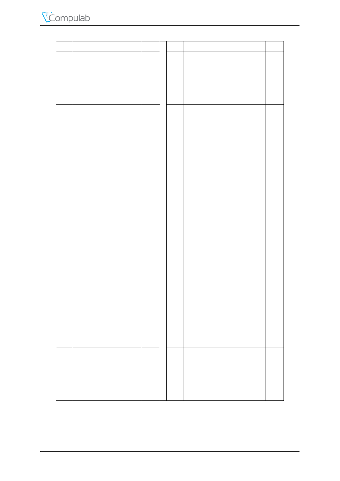
Carrier board Interface
Pin #
CL-SOM-AM57x Signal Name
Ref. Pin #
CL-SOM-AM57x Signal Name
Ref.
129
VIN1A_HSYNC0
UART6_TXD
I2C5_SCL
PR2_PRU1_GPI9
PR2_PRU1_GPO9
GPIO5_3
4.2
4.12
4.14
4.21.5
4.21.5
4.23
130
VOUT1_D11
VIN1A_D11
VIN2A_D11
VIN3A_D11
VIN4A_D11
PR2_UART0_CTS_N
PR2_PRU0_GPI8
PR2_PRU0_GPO8
GPIO8_11
4.1.1
4.2
4.2
4.2
4.2
4.21.2
4.21.5
4.21.5
4.23
131
PCIE_RXP0
04.3
132
VSYS
5.1
133
PCIE_RXN0
04.3
134
VOUT1_D12
VIN1A_D12
VIN2A_D12
VIN3A_D12
VIN4A_D12
PR2_UART0_RTS_N
PR2_PRU0_GPI9
PR2_PRU0_GPO9
GPIO8_12
4.1.1
4.2
4.2
4.2
4.2
4.21.2
4.21.5
4.21.5
4.23
135
VIN1A_VSYNC0
UART6_RXD
I2C5_SDA
PR2_PRU1_GPI8
PR2_PRU1_GPO8
GPIO5_2
4.2
4.12
4.14
4.21.5
4.21.5
4.23
136
VOUT1_D13
VIN1A_D13
VIN2A_D13
VIN3A_D13
VIN4A_D13
PR2_UART0_RXD
PR2_PRU0_GPI10
PR2_PRU0_GPO10
GPIO8_13
4.1.1
4.2
4.2
4.2
4.2
4.21.2
4.21.5
4.21.5
4.23
137
VIN1A_D7
MCASP2_ACLKX
PR2_PRU0_GPI18
PR2_PRU0_GPO18
4.2
4.10
4.21.5
4.21.5
138
VOUT1_D14
VIN1A_D14
VIN2A_D14
VIN3A_D14
VIN4A_D14
PR2_UART0_TXD
PR2_PRU0_GPI11
PR2_PRU0_GPO11
GPIO8_14
4.1.1
4.2
4.2
4.2
4.2
4.21.2
4.21.5
4.21.5
4.23
139
VIN1A_D10
VIN2A_D10
VIN4A_D10
MCASP2_AXR0
4.2
4.2
4.2
4.10
140
VOUT1_D15
VIN1A_D15
VIN2A_D15
VIN3A_D15
VIN4A_D15
PR2_ECAP0_ECAP_CAPIN_APWM_O
PR2_PRU0_GPI12
PR2_PRU0_GPO12
GPIO8_15
4.1.1
4.2
4.2
4.2
4.2
4.21.4
4.21.5
4.21.5
4.23
141
GND
5.1
142
VOUT1_D18
VIN1A_D2
VIN2A_D2
VIN3A_D2
VIN4A_D2
PR2_EDIO_DATA_IN2
PR2_EDIO_DATA_OUT2
PR2_PRU0_GPI15
PR2_PRU0_GPO15
GPIO8_18
4.1.1
4.2
4.2
4.2
4.2
4.21.3
4.21.3
4.21.5
4.21.5
4.23
143
VIN1A_D11
VIN2A_D11
VIN4A_D11
MCASP2_AXR1
4.2
4.2
4.2
4.10
144
VOUT1_D19
VIN1A_D3
VIN2A_D3
VIN3A_D3
VIN4A_D3
PR2_EDIO_DATA_IN3
PR2_EDIO_DATA_OUT3
PR2_PRU0_GPI16
PR2_PRU0_GPO16
GPIO8_19
4.1.1
4.2
4.2
4.2
4.2
4.21.3
4.21.3
4.21.5
4.21.5
4.23
Revised April 2018 CL-SOM-AM57x 71
Page 72
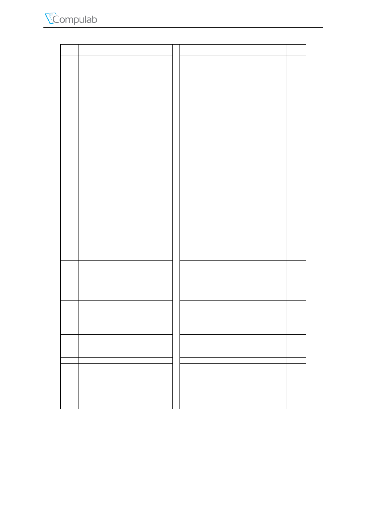
Carrier board Interface
Pin #
CL-SOM-AM57x Signal Name
Ref. Pin #
CL-SOM-AM57x Signal Name
Ref.
145
VIN1A_D6
MCASP2_FSX
PR2_PRU0_GPI19
PR2_PRU0_GPO19
4.2
4.10
4.21.5
4.21.5
146
VOUT1_D20
VIN1A_D4
VIN2A_D4
VIN3A_D4
VIN4A_D4
PR2_EDIO_DATA_IN4
PR2_EDIO_DATA_OUT4
PR2_PRU0_GPI17
PR2_PRU0_GPO17
GPIO8_20
4.1.1
4.2
4.2
4.2
4.2
4.21.3
4.21.3
4.21.5
4.21.5
4.23
147
MMC4_CMD
UART1_RTSN
UART9_TXD
GPIO7_25
4.11
4.12
4.12
4.23
148
VOUT1_D21
VIN1A_D5
VIN2A_D5
VIN3A_D5
VIN4A_D5
PR2_EDIO_DATA_IN5
PR2_EDIO_DATA_OUT5
PR2_PRU0_GPI18
PR2_PRU0_GPO18
GPIO8_21
4.1.1
4.2
4.2
4.2
4.2
4.21.3
4.21.3
4.21.5
4.21.5
4.23
149
MMC4_DAT3
UART1_RIN
UART10_TXD
UART2_RTSN
UART3_IRTX
UART3_TXD
GPIO1_17
4.11
4.12
4.12
4.12
4.12
4.12
4.23
150
VSYS
5.1
151
MMC4_DAT2
UART1_DTRN
UART10_RXD
UART2_CTSN
UART3_RXD
GPIO1_16
4.11
4.12
4.12
4.12
4.12
4.23
152
VIN1A_D0
MCASP5_AHCLKX
HDQ0
PR2_MII1_COL
PR2_PRU1_GPI5
PR2_PRU1_GPO5
TIMER13
GPIO6_17
CLKOUT2
4.2
4.10
4.17
4.21.1
4.21.5
4.21.5
4.22
4.23
5.2.2
153
MMC4_DAT1
UART1_DSRN
UART2_TXD
UART3_RTSN
UART3_SD
GPIO7_27
4.11
4.12
4.12
4.12
4.12
4.23
154
VIN1A_CLK0
MCASP2_AHCLKX
PR2_MII1_CRS
PR2_PRU1_GPI6
PR2_PRU1_GPO6
TIMER14
GPIO6_18
4.2
4.10
4.21.1
4.21.5
4.21.5
4.22
4.23
155
MMC4_DAT0
UART1_DCDN
UART2_RXD
UART3_CTSN
UART3_RCTX
GPIO7_26
4.11
4.12
4.12
4.12
4.12
4.23
156
HUB_USB_PWREN
USB2_DRVVBUS
TIMER15
GPIO6_13
4.6
4.6
4.22
4.23
157
MMC4_CLK
UART1_CTSN
UART9_RXD
GPIO7_24
4.11
4.12
4.12
4.23
158
HUBUSB3_DN
4.6
159
GND
5.1
160
HUBUSB3_DP
4.6
161
VOUT1_FLD
VIN1A_CLK0
VIN1A_CLK0
VIN2A_CLK0
VIN3A_CLK0
VIN4A_CLK0
SPI3_CS1
GPIO4_21
4.1.1
4.2
4.2
4.2
4.2
4.2
0
4.23
162
VIN4A_D2
HUB_USB_OCN
GPIO5_4
4.2
4.6
4.23
Revised April 2018 CL-SOM-AM57x 72
Page 73
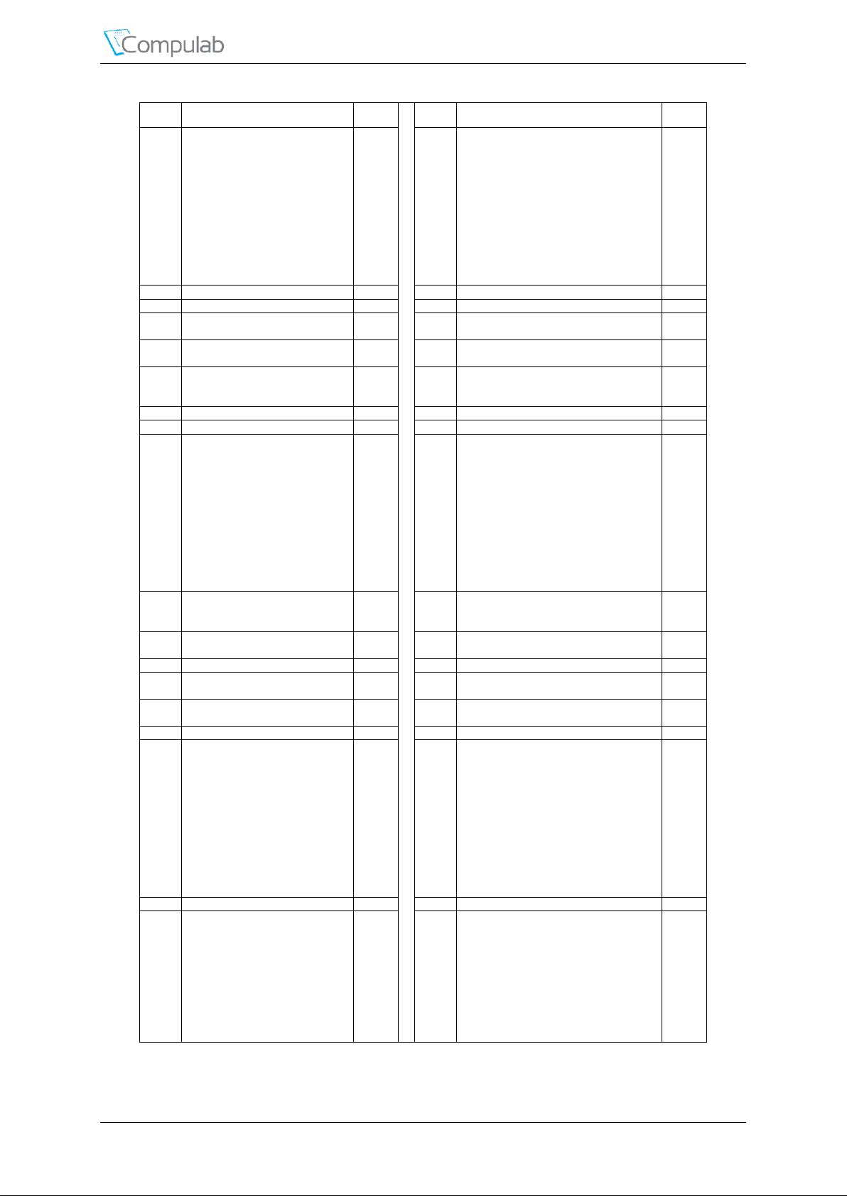
Carrier board Interface
Pin #
CL-SOM-AM57x Signal Name
Ref. Pin #
CL-SOM-AM57x Signal Name
Ref.
163
VIN1A_D0
VIN2B_D0
VIN2B_D0
VIN5A_D0
MMC3_DAT5
UART10_TXD
SPI4_D1
EHRPWM3B
PR2_MII1_RXD2
PR2_PRU0_GPI9
PR2_PRU0_GPO9
GPIO1_23
4.2
4.2
4.2
4.2
4.11
4.12
0
4.18
4.21.1
4.21.5
4.21.5
4.23
164
HUBUSB2_DN
4.6
165
PWRON
5.2.1
166
HUBUSB2_DP
4.6
167
PCIE_RXN1
04.3
168
VSYS
5.1
169
PCIE_RXP1
04.3
170
HUBUSB1_DN
USB2_DM
4.6
4.6
171
COLD_RESET_IN
5.3
172
HUBUSB1_DP
USB2_DP
4.6
4.6
173
PCIE_TXN1
04.3
174
VIN1A_D3
VIN2A_D3
VIN4A_D3
4.2
4.2
4.2
175
PCIE_TXP1
04.3
176
USB1_DP
4.5
177
GND
5.1
178
USB1_DM
4.5
179
VIN1A_VSYNC0
VIN2B_CLK1
VIN2B_CLK1
VIN5A_VSYNC0
MMC3_DAT7
UART10_RTSN
SPI4_CS0
ECAP3_IN_PWM3_OUT
PR2_MII1_RXD0
PR2_PRU0_GPI11
PR2_PRU0_GPO11
GPIO1_25
4.2
4.2
4.2
4.2
4.11
4.12
0
4.19
4.21.1
4.21.5
4.21.5
4.23
180
RESERVED
181
SATA1_LED
SPI1_CS1
GPIO7_11
4.4
0
4.23
182
PCIE_RXP1
USB_RXP0
04.3
4.5
183
VCC_RTC
5.1
184
PCIE_RXN1
USB_RXN0
4.3
4.5
185
ALT_BOOT
5.4
186
VSYS
5.1
187
RESETN
5.3
188
PCIE_TXP1
USB_TXP0
4.3
4.5
189
EEPROM_WP
5.2.3
190
PCIE_TXN1
USB_TXN0
4.3
4.5
191
MICBIAS
4.9
192
GPIO1_1
4.23
193
VIN1A_CLK0
VIN2A_CLK0
VIN4A_CLK0
MICIN
MCASP3_AHCLKX
TIMER15
GPIO6_19
4.2
4.2
4.2
4.9
4.10
4.22
4.23
194
VIN1A_HSYNC0
VIN2B_DE1
VIN2B_DE1
VIN5A_HSYNC0
MMC3_DAT6
UART10_CTSN
SPI4_D0
EHRPWM3_TRIPZONE_INPUT
PR2_MII1_RXD1
PR2_PRU0_GPI10
PR2_PRU0_GPO10
GPIO1_24
4.2
4.2
4.2
4.2
4.11
4.12
0
4.18
4.21.1
4.21.5
4.21.5
4.23
195
AUD_GND
5.1
196
RESERVED
197
VIN1A_D0
VIN1A_FLD0
VIN5A_FLD0
RLINEIN
MCASP3_AXR1
UART5_TXD
UART7_RTSN
PR2_MII1_RXLINK
PR2_PRU0_GPI15
PR2_PRU0_GPO15
4.2
4.2
4.2
4.9
4.10
4.12
4.12
4.21.1
4.21.5
4.21.5
198
ENABLE1
5.2.1
Revised April 2018 CL-SOM-AM57x 73
Page 74
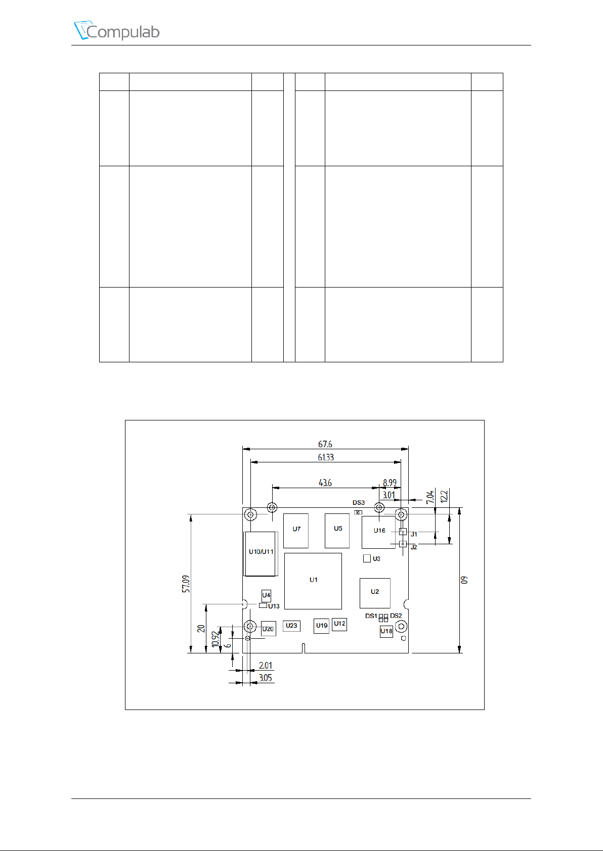
Carrier board Interface
Pin #
CL-SOM-AM57x Signal Name
Ref. Pin #
CL-SOM-AM57x Signal Name
Ref.
199
VIN1A_D3
LLINEIN
MCASP3_ACLKR
MCASP3_ACLKX
UART7_RXD
PR2_PRU0_GPI12
PR2_PRU0_GPO12
GPIO5_13
4.2
4.9
4.10
4.10
4.12
4.21.5
4.21.5
4.23
200
USB1_DRVVBUS
TIMER16
GPIO6_12
4.5
4.22
4.23
201
VIN1A_D1
RHPOUT
MCASP3_AXR0
UART5_RXD
UART7_CTSN
PR2_MII1_RXER
PR2_PRU0_GPI14
PR2_PRU0_GPO14
4.2
4.9
4.10
4.12
4.12
4.21.1
4.21.5
4.21.5
202
VIN1A_D1
VIN2B_D1
VIN2B_D1
VIN5A_D1
MMC3_DAT4
UART10_RXD
SPI4_SCLK
EHRPWM3A
PR2_MII1_RXD3
PR2_PRU0_GPI8
PR2_PRU0_GPO8
GPIO1_22
PER_PWREN
4.2
4.2
4.2
4.2
4.11
4.12
0
4.18
4.21.1
4.21.5
4.21.5
4.23
5.2.1
203
VIN1A_D2
LHPOUT
MCASP3_FSR
MCASP3_FSX
UART7_TXD
PR2_PRU0_GPI13
PR2_PRU0_GPO13
GPIO5_14
4.2
4.9
4.10
4.10
4.12
4.21.5
4.21.5
4.23
204
VSYS
5.1
6.2 Mechanical Drawings
Figure 4 CL-SOM-AM57x Top
Revised April 2018 CL-SOM-AM57x 74
Page 75
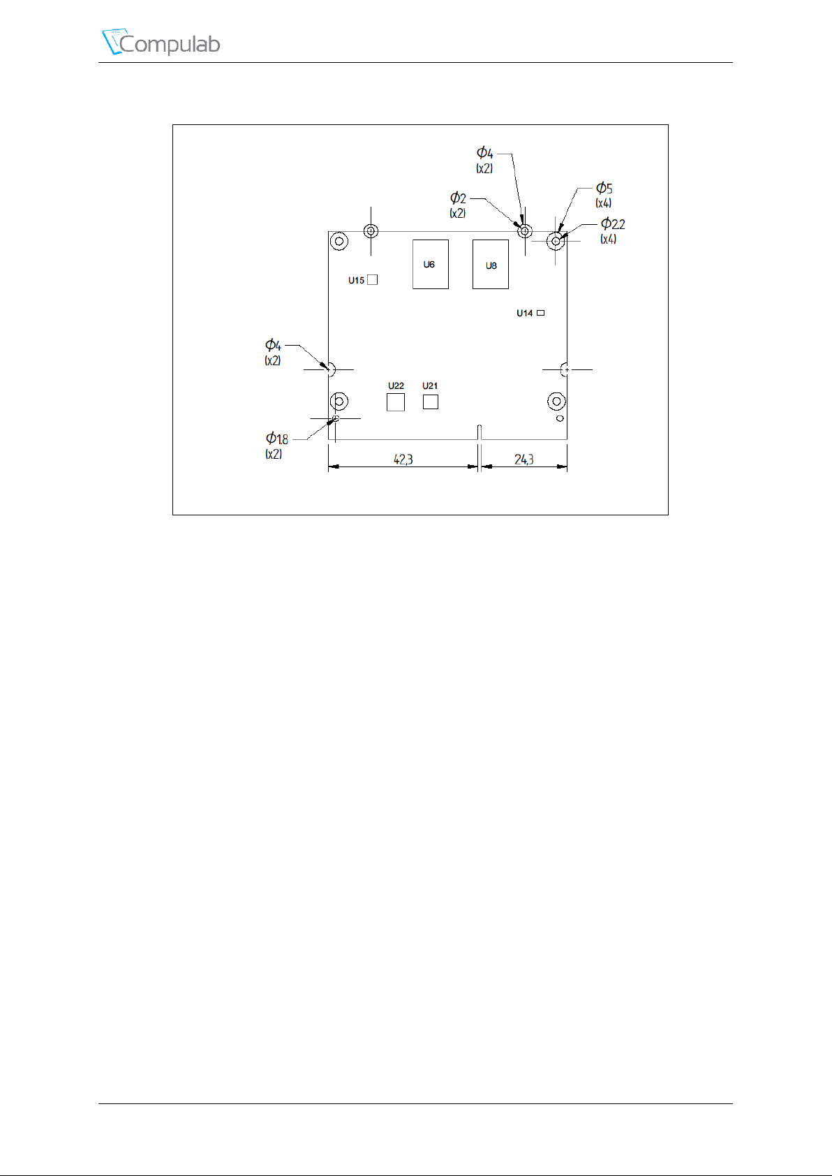
Carrier board Interface
Figure 5 CL-SOM-AM57x bottom
1. All dimensions are in millimeters.
2. Max height of components on module Bottom Side is 2.8mm.
3. Baseboard connectors provide 2.8mm board-to-board clearance.
4. Board thickness is 1.0mm.
Mechanical drawings are available in DXF format at
http://www.compulab.com/products/computer-on-modules/cl-som-am57x-ti-am5728-am5718system-on-module/#devres
6.3 Heat Spreader and Cooling Solutions
CompuLab provides CL-SOM-AM57x with a dedicated heat-spreader assembly. The CL-SOMAM57x heat-spreader has been designed to act as a thermal interface and should be used in
conjunction with a heat-sink or an external cooling solution. A cooling solution must be provided
to ensure that under worst-case conditions the temperature on any spot of the heat-spreader
surface is maintained according to the CL-SOM-AM57x temperature specifications. Various
thermal management solutions can be used with the heat-spreader, including active and passive
approaches.
Documentation and CAD drawings for the CL-SOM-AM57x heat-spreader and cooling solutions
are provided at http://www.compulab.com/products/computer-on-modules/cl-som-am57x-ti-
am5728-am5718-system-on-module/#devres.
6.4 Standoffs/Spacers
CL-SOM-AM57x has two mounting half holes to physically secure the CoM/SoM to the carrier
board. Secure CL-SOM-AM57x to the carrier board by mounting two spacers with any adequate
screws and nuts. Spacers must comply with the following specification:
M2x0.4 thread, 2.2±0.2 mm length
Revised April 2018 CL-SOM-AM57x 75
Page 76
Operational Characteristics
Parameter
Condition
Min
Max
Unit
Main power supply voltage (VSYS)
-0.3 6 V
Backup battery supply voltage (BACKUP_BAT)
-0.3 6 V
VBUS input
-2
20
V
LDOUSB_IN2 (LDOUSB regulator input voltage in
PMIC)
-0.3
20
V
Parameter
Limitations
Min
Typ
Max
Unit
Main power supply voltage (VSYS)
Normal operation
3.8 5.25 V Backup battery supply voltage (VCC_RTC)
1.4 5.5
V
VBUS input
0
5.0
5.25
V
LDOUSB_IN2 (LDOUSB regulator input
voltage in PMIC)
4.3 5.25
V
Parameter
Operating
Conditions
Min
Typ
Max
Unit
Multifunctional Digital I/O
VIH
2
V
VIL
0.8 V VOH
IOH=100µA
3.1
V
VOL
IOL=100µA
0.2
V
PARAMETER
ESD Performance
V
ESD
ESD stress voltage
±1kV Human Body Model (HBM)
±250V CDM (Charged Device Model)
7 OPERATIONAL CHARACTERISTICS
7.1 Absolute Maximum Ratings
Table 69 Absolute Maximum ratings
NOTE: Exceeding the absolute maximum ratings may damage the device.
7.2 Recommended Operating Conditions
Table 70 Recommended Operating Conditions
7.3 DC Electrical Characteristics
Table 71 DC Electrical Characteristics
7.4 ESD Performance
Table 72 ESD Performance
Revised April 2018 CL-SOM-AM57x 76
Page 77
Operational Characteristics
Range
Temp.
Description
Commercial
0o to 70o C
Sample boards from each batch are tested for the lower and upper
temperature limits. Individual boards are not tested.
Extended
-20o to 70o C
Every board undergoes a short test for the lower limit (-20o C)
qualification.
Industrial
-40o to 85o C
Every board is extensively tested for both lower and upper limits
and at several midpoints.
7.5 Operating Temperature Ranges
The CL-SOM-AM57x is available with three options of operating temperature range.
Table 73 CL-SOM-AM57x Temperature Range Options
Revised April 2018 CL-SOM-AM57x 77
Page 78
Application Notes
8 APPLICATION NOTES
8.1 Carrier Board Design Guidelines
Ensure that all VSYS and GND power pins are connected.
Major power rails - VSYS and GND must be implemented by planes, rather than traces.
Using at least two planes is essential to ensure the system signal quality, because the planes
provide a current return path for all interface signals.
It is recommended to put several 100nF and 10/100uF capacitors between VSYS and GND
near the mating connectors.
It is recommended to connect the standoff holes of the carrier board to GND, in order to
improve EMC.
Except for a power connection, no other connection is mandatory for CL-SOM-AM57x
operation. All power-up circuitry and all required pullups/pulldowns are available onboard
CL-SOM-AM57x.
If for some reason you decide to place an external pullup or pulldown resistor on a certain
signal (for example - on the GPIOs), first check the documentation of that signal provided
in this manual. Certain signals have on-board pullup/pulldown resistors required for proper
initialization. Overriding their values by external components will disable board operation.
You must be familiar with signal interconnection design rules. There are many sensitive
groups of signals. For example:
Ethernet, SATA, USB and more signals must be routed in differential pairs and by a
controlled impedance trace.
Audio input must be decoupled from possible sources of carrier board noise.
Be careful when placing components under the CL-SOM-AM57x module. The carrier
board interface connector provides 1mm mating height. Bear in mind that there are
components on the underside of the CL-SOM-AM57x.
Refer to the SB-SOM-AM57x carrier board reference design schematics.
8.2 Carrier Board Troubleshooting
Using grease solvent and a soft brush, clean the contacts of the mating connectors of both
the module and the carrier board. Remnants of soldering paste can prevent proper contact.
Take care to let the connectors and the module dry entirely before re-applying power –
otherwise corrosion may occur.
Using an oscilloscope, check the voltage levels and quality of the VSYS power supply. It
should be as specified in section 7.2. Check that there is no excessive ripple or glitches.
First perform the measurements without plugging in the module. Then plug in the module
and measure again. Measurement should be performed on the pins of the mating connector.
Using an oscilloscope, verify that the GND pins of the mating connector are indeed at zero
voltage level and that there is no ground bouncing. The module must be plugged in during
the test.
Create a "minimum system" - only power, mating connectors, the module and a serial
interface.
Check if the system starts properly. In system larger than the minimum, possible sources of
disturbance could be:
Devices improperly driving the local bus
External pullup/pulldown resistors overriding the module on-board values, or any
other component creating the same "overriding" effect
Faulty power supply
In order to avoid possible sources of disturbance, it is strongly recommended to start with a
minimal system and then to add/activate off-board devices one by one.
Revised April 2018 CL-SOM-AM57x 78
Page 79
Application Notes
Vendor
P/N
Package
UDE
RB1-125BAK1A
Integrated RJ45
UNE
U50{79}G8-09-B122-B12-BT
Integrated, Dual RJ45
YDS
45F-10202GDD2
Integrated, Dual USB + RJ45
Check for the existence of soldering shorts between pins of mating connectors. Even if the
signals are not used on the carrier board, shorting them on the connectors can disable the
module operation. An initial check can be performed using a microscope. However, if
microscope inspection finds nothing, it is advisable to check using an X-ray, because often
solder bridges are deep beneath the connector body. Note that solder shorts are the most
probable factor to prevent a module from booting.
Check possible signal short circuits due to errors in carrier board PCB design or assembly.
Improper functioning of a customer carrier board can accidentally delete boot-up code
from CL-SOM-AM57x, or even damage the module hardware permanently. Before every
new attempt of activation, check that your module is still functional with CompuLab SBSOM-AM57x carrier board.
It is recommended to assemble more than one carrier board for prototyping, in order to
ease resolution of problems related to specific board assembly.
8.3 Ethernet Magnetics Implementation
8.3.1 Magnetics Selection
Refer to the table below for compatible magnetics. The list of “Qualified Magnetics” contains
magnetics verified for proper functional operation by CompuLab. Designers should test and
qualify all magnetics before using them in an application.
Table 74 Qualified Magnetics
8.3.2 Magnetics Connection
For magnetic modules connection, please refer to the SB-SOM-AM57x reference design
schematics.
Revised April 2018 CL-SOM-AM57x 79
 Loading...