

Page 1

Technical Reference Guide
For the
Compaq iPAQ Series of
Desktop Personal Computers
Covers iPAQ 1.0, 1.2, and 2.0 Models
Page 2

This hardcopy is designed to be placed into a standard 3-ring binder. Provided below is a title block that
can be copied and cut out and placed into the slip or taped onto the edge of the binder.
iPAQ Series of Desktop Personal Computers
TRG
Page 3

Reader Feedback
Please feel free to send any quest i ons, suggestions, co rrections, o r comments regarding this
document please to the following email address:
CPCG.Training@compaq.com
When responding, please state the title of the referenced document.
Page 4

Page 5

Technical Reference Guide
NOTICE
The information in this document is subject to change without notice.
COMPAQ COMPUTER CORPORATION SHALL NOT BE LIABLE FOR TECHNICAL OR
EDITORIAL ERRORS OR OMISSIONS HEREIN; NOR FOR INCIDENTAL OR
CONSEQUENTIAL DAMAGES RESULTING FROM THE FURNISHING, PERFORMANCE,
OR USE OF THIS MATERIAL. IT IS THE RESPONSIBILITY OF MANUFACTURERS TO
ENSURE THAT DEVICES DESIGNED TO BE USED WITH COMPAQ PRODUCTS
COMPLY WITH FCC CLASS B EMISSIONS REQUIREMENTS.
This guide contains information protected by copyright. Except for use as a reference for the
described Compaq product, no part of this document may be photocopied or reproduced in any
form without prior written consent from Compaq Computer Corporation.
2000 Compaq Computer Corporation
All rights reserved.
Compaq, t he Compaq logo ar e registered in the U.S. Patent and Trademark Office.
iPAQ is a trademark of Compaq Information Technologies Group, L.P.
Microsoft, Windows, Windows NT, and other names of Microsoft products referenced herein are trademarks or registered
trademarks of Microsoft Corporation.
Alert on LAN, Wake on LAN, and Ethernet names/brands are the property of IBM Corporation.
Intel and Pentium are registered trademarks of Intel Corporation. Celeron and MMX are trademarks of Intel Corporation.
Product names mentioned in this document may be trademarks and/or registered trademarks of other companies.
For more information regarding specifications and Compaq-specific parts please contact Compaq
Computer Corporation at http://www.compaq.com .
Technical Reference Guide
For the
Compaq iPAQ Series of Desktop Personal Computers
Second Edition – February 2001
Document Number 127M-0300B-WWEN
Compaq iPAQ Series of Desktop Personal Computers
i
Second Edition - February 2001
Page 6

Technical Reference Guide
Compaq iPAQ Series of Desktop Personal Computers
ii
Second Edition –- February 2001
Page 7

Technical Reference Guide
TABLE OF CONTENTS
CHAPTER 1 INTRODUCTION...................................................................................................................
1.1 ABOUT THIS GUIDE................................................................................................................ 1-1
1.1.1 USING THIS GUIDE.......................................................................................................... 1-1
1.2 ADDITIONAL INFORMATION SOURCES............................................................................. 1-2
1.3 MODEL NUMBERING CONVENTION................................................................................... 1-2
1.4 SERIAL NUMBER..................................................................................................................... 1-2
1.5 NOTATIONAL CONVENTIONS.............................................................................................. 1-3
1.5.1 VALUES ............................................................................................................................. 1-3
1.5.2 RANGES............................................................................................................................. 1-3
1.5.3 REGISTER NOTATION AND USAGE............................................................................. 1-3
1.5.4 BIT NOTATION AND BYTE VALUES............................................................................ 1-3
1.6 COMMON ACRONYMS AND ABBREVIATIONS................................................................. 1-4
CHAPTER 2 SYSTEM OVERVIEW...........................................................................................................
2.1 INTRODUCTION....................................................................................................................... 2-1
2.2 FEATURES AND OPTIONS...................................................................................................... 2-2
2.2.1 STANDARD FEATURES...................................................................................................2-2
2.2.2 OPTIONS............................................................................................................................ 2-3
2.3 MECHANICAL DESIGN........................................................................................................... 2-4
2.3.1 CABINET LAYOUTS ........................................................................................................ 2-4
2.3.2 CHASSIS LAYOUTS......................................................................................................... 2-6
2.3.3 SYSTEM BOARD LAYOUTS........................................................................................... 2-8
2.4 SYSTEM ARCHITECTURE.................................................................................................... 2-10
2.4.1 IPAQ 1.0/1.2 ARCHITECTURE....................................................................................... 2-10
2.4.2 IPAQ 2.0 ARCHITECTURE............................................................................................. 2-12
2.4.3 PROCESSORS.................................................................................................................. 2-14
2.4.4 CHIPSET........................................................................................................................... 2-16
2.4.5 SUPPORT COMPONENTS.............................................................................................. 2-17
2.4.6 SYSTEM MEMORY......................................................................................................... 2-17
2.4.7 MASS STORAGE............................................................................................................. 2-18
2.4.8 SERIAL AND PARALLEL INTERFACES...................................................................... 2-18
2.4.9 UNIVERSAL SERIAL BUS INTERFACE ...................................................................... 2-18
2.4.10 GRAPHICS SUBSYSTEM............................................................................................... 2-18
2.4.11 AUDIO SUBSYSTEM...................................................................................................... 2-19
2.5 SPECIFICATIONS ................................................................................................................... 2-19
CHAPTER 3 PROCESSOR/MEMORY SUBSYSTEM.............................................................................
3.1 INTRODUCTION....................................................................................................................... 3-1
3.2 PROCESSOR .............................................................................................................................. 3-2
3.2.1 CELERON PROCESSOR................................................................................................... 3-2
3.2.2 PENTIUM III PROCESSOR............................................................................................... 3-3
3.2.3 PROCESSOR UPGRADING.............................................................................................. 3-4
3.3 MEMORY SUBSYSTEM........................................................................................................... 3-5
3.4 SUBSYSTEM CONFIGURATION............................................................................................ 3-8
Compaq iPAQ Series of Desktop Personal Computers
iii
Second Edition - February 2001
Page 8

Technical Reference Guide
CHAPTER 4 SYSTEM SUPPORT...............................................................................................................
4.1 INTRODUCTION....................................................................................................................... 4-1
4.2 PCI BUS OVERVIEW................................................................................................................ 4-2
4.2.1 PCI BUS TRANSACTIONS............................................................................................... 4-3
4.2.2 PCI SUB-BUSSES.............................................................................................................. 4-5
4.2.3 PCI CONFIGURATION..................................................................................................... 4-6
4.3 SYSTEM RESOURCES .............................................................................................................4-7
4.3.1 INTERRUPTS..................................................................................................................... 4-7
4.3.2 DIRECT MEMORY ACCESS.......................................................................................... 4-10
4.4 SYSTEM CLOCK DISTRIBUTION........................................................................................ 4-11
4.5 REAL-TIME CLOCK AND CONFIGURATION MEMORY ................................................. 4-11
4.5.1 CLEARING CMOS........................................................................................................... 4-12
4.5.2 CMOS ARCHIVE AND RESTORE................................................................................. 4-12
4.5.3 STANDARD CMOS LOCATIONS.................................................................................. 4-13
4.6 SYSTEM MANAGEMENT...................................................................................................... 4-22
4.6.1 SECURITY FUNCTIONS ................................................................................................ 4-22
4.6.2 POWER MANAGEMENT................................................................................................ 4-23
4.6.3 SYSTEM STATUS ........................................................................................................... 4-24
4.6.4 TEMPERATURE SENSING AND COOLING................................................................ 4-25
4.7 REGISTER MAP AND MISCELLANEOUS FUNCTIONS.................................................... 4-26
4.7.1 SYSTEM I/O MAP ........................................................................................................... 4-26
4.7.2 82801 ICH GENERAL PURPOSE FUNCTIONS............................................................ 4-27
4.7.3 I/O CONTROLLER FUNCTIONS .................................................................................. 4-28
4.7.4 820802 FWH FUNCTIONS.............................................................................................. 4-30
CHAPTER 5 INPUT/OUTPUT INTERFACES..........................................................................................
5.1 INTRODUCTION....................................................................................................................... 5-1
5.2 ENHANCED IDE INTERFACE................................................................................................. 5-1
5.2.1 IDE PROGRAMMING....................................................................................................... 5-1
5.2.2 PRIMARY IDE INTERFACE............................................................................................. 5-3
5.2.3 SECONDARY IDE INTERFACE.......................................................................................5-4
5.3 DISKETTE DRIVE INTERFACE.............................................................................................. 5-5
5.4 SERIAL INTERFACE................................................................................................................ 5-6
5.4.1 RS-232 INTERFACE.......................................................................................................... 5-6
5.4.2 SERIAL TEST INTERFACE............................................................................................. 5-7
5.4.3 SERIAL INTERFACE PROGRAMMING ......................................................................... 5-7
5.5 PARALLEL INTERFACE.......................................................................................................... 5-9
5.5.1 STANDARD PARALLEL PORT MODE........................................................................... 5-9
5.5.2 ENHANCED PARALLEL PORT MODE .......................................................................... 5-9
5.5.3 EXTENDED CAPABILITIES PORT MODE .................................................................. 5-10
5.5.4 PARALLEL INTERFACE PROGRAMMING................................................................. 5-10
5.5.5 PARALLEL INTERFACE CONNECTOR....................................................................... 5-14
5.6 KEYBOARD/POINTING DEVICE INTERFACE................................................................... 5-15
5.6.1 KEYBOARD INTERFACE OPERATION....................................................................... 5-15
5.6.2 POINTING DEVICE INTERFACE OPERATION .......................................................... 5-17
5.6.3 KEYBOARD/POINTING DEVICE INTERFACE PROGRAMMING........................... 5-17
5.6.4 KEYBOARD/POINTING DEVICE INTERFACE CONNECTOR.................................. 5-21
5.7 UNIVERSAL SERIAL BUS INTERFACE .............................................................................. 5-22
5.7.1 USB DATA FORMATS.................................................................................................... 5-23
5.7.2 USB PROGRAMMING.................................................................................................... 5-24
5.7.3 USB CONNECTOR.......................................................................................................... 5-25
5.7.4 USB CABLE DATA......................................................................................................... 5-25
Compaq iPAQ Series of Desktop Personal Computers
iv
Second Edition –- February 2001
Page 9

Technical Reference Guide
5.8 AUDIO SUBSYSTEM..............................................................................................................5-26
5.8.1 FUNCTIONAL ANALYSIS............................................................................................. 5-26
5.8.2 AC97 AUDIO CONTROLLER......................................................................................... 5-28
5.8.3 AC97 LINK BUS ..............................................................................................................5-28
5.8.4 AUDIO CODEC ................................................................................................................5-29
5.8.5 AUDIO PROGRAMMING............................................................................................... 5-30
5.8.6 AUDIO SPECIFICATIONS.............................................................................................. 5-31
5.9 NETWORK INTERFACE CONTROLLER............................................................................. 5-32
5.9.1 WAKE ON LAN............................................................................................................... 5-33
5.9.2 ALERT ON LAN...............................................................................................................5-33
5.9.3 POWER MANAGEMENT SUPPORT............................................................................. 5-34
5.9.4 NIC PROGRAMMING..................................................................................................... 5-35
CHAPTER 6 GRAPHICS SUBSYSTEM.....................................................................................................
6.1 INTRODUCTION....................................................................................................................... 6-1
6.1.1 FEATURE SUMMARY...................................................................................................... 6-1
6.2 FUNCTIONAL DESCRIPTION................................................................................................. 6-2
6.2.1 DISPLAY MODES ............................................................................................................. 6-4
6.3 PROGRAMMING....................................................................................................................... 6-5
6.4 MONITOR POWER MANAGEMENT CONTROL.................................................................. 6-5
6.5 MONITOR CONNECTOR......................................................................................................... 6-6
6.6 UPGRADING GRAPHICS......................................................................................................... 6-6
CHAPTER 7 POWER SUPPLY AND DISTRIBUTION...........................................................................
7.1 INTRODUCTION....................................................................................................................... 7-1
7.2 POWER SUPPLY ASSEMBLY/CONTROL ............................................................................. 7-1
7.2.1 POWER SUPPLY ASSEMBLY......................................................................................... 7-2
7.2.2 POWER CONTROL ........................................................................................................... 7-3
7.3 POWER DISTRIBUTION .......................................................................................................... 7-4
7.3.1 3.3/5/12 VDC DISTRIBUTION.......................................................................................... 7-4
7.3.2 LOW VOLTAGE DISTRIBUTION ................................................................................... 7-6
7.4 SIGNAL DISTRIBUTION..........................................................................................................7-7
CHAPTER 8 BIOS ROM..............................................................................................................................
8.1 INTRODUCTION....................................................................................................................... 8-1
8.2 IPAQ 2.0 FEATURES................................................................................................................. 8-2
8.3 DESKTOP MANAGEMENT SUPPORT................................................................................... 8-3
8.3.1 SYSTEM ID........................................................................................................................ 8-4
8.3.2 EDID RETRIEVE ............................................................................................................... 8-5
8.3.3 DRIVE FAULT PREDICTION........................................................................................... 8-5
8.3.4 SYSTEM MAP RETRIEVAL............................................................................................. 8-6
8.3.5 FLASH ROM FUNCTIONS............................................................................................... 8-7
8.3.6 POWER BUTTON FUNCTIONS....................................................................................... 8-7
8.3.7 ACCESSING CMOS........................................................................................................... 8-8
8.3.8 ACCESSING CMOS FEATURE BITS .............................................................................. 8-8
8.3.9 SECURITY FUNCTIONS ................................................................................................ 8-10
8.4 MEMORY DETECTION AND CONFIGURATION............................................................... 8-11
Compaq iPAQ Series of Desktop Personal Computers
v
Second Edition - February 2001
Page 10

Technical Reference Guide
8.5 PNP SUPPORT ......................................................................................................................... 8-12
8.5.1 SMBIOS............................................................................................................................ 8-13
8.6 POWER MANAGEMENT FUNCTIONS................................................................................ 8-14
8.6.1 INDEPENDENT PM SUPPORT ...................................................................................... 8-14
8.6.2 ACPI SUPPORT................................................................................................................ 8-15
8.6.3 APM 1.2 SUPPORT.......................................................................................................... 8-15
8.7 USB LEGACY SUPPORT........................................................................................................ 8-17
8.8 BIOS UPGRADING.................................................................................................................. 8-18
APPENDIX A ERROR MESSAGES AND CODES....................................................................................
A.1 INTRODUCTION.......................................................................................................................A-1
A.2 BEEP/KEYBOARD LED CODES..............................................................................................A-1
A.3 POWER-ON SELF TEST (POST ) MESSAGES ........................................................................A-2
A.4 SYSTEM ERROR MESSAGES (1
A.5. MEMORY ERROR MESSAGES (2
A.6 KE Y BOARD ERROR MESSAGES (30
A.7 PRINTER ERROR MESSAGES (4
A.8 VIDEO (GRAPHICS) ERROR MESSAGES (5
A.9 DISKET TE DRIVE ERROR MESSAGES (6
A.10 SERIAL INTERFACE ERROR MESSAGES (11
A.11 MODEM COMMUNICATIONS ERROR MESSAGES (12
A.12 SYSTEM STATUS ERROR MESSAGES (16
A.13 HARD DRIVE ERROR MESSAGES (17
A.14 HARD DRIVE ERROR MESSAGES (19
A.15 VIDEO (GRAPHICS) ERROR MESSAGES (24
A.16 AUDIO ERROR MESSAGES (3206A.17 DVD/CD-ROM ERROR MESSAGES (33
A.18 NETWORK INTERFACE ERROR MESSAGES (60
A.19 SCSI INTERFACE ERROR MESSAGES (65
A.20 POINTING DEVICE INTERFACE ERROR MESSAGES (8601-
) .................................................................................A-3
XX-XX
) ...............................................................................A-4
XX-XX
) ...........................................................................A-4
X-XX
).................................................................................A-5
XX-XX
)..............................................................A-5
XX-XX
).................................................................A-6
XX-XX
)...........................................................A-6
XX-XX
)..........................................A-7
XX-XX
) ...............................................................A-8
XX-XX
).......................................................................A-8
XX-XX
).......................................................................A-9
XX-XX
)............................................................A-9
XX-XX
).................................................................................A-10
XX
)....................................................................A-10
XX-XX
) ..................................................A-10
XX-XX
, 66XX-XX, 67XX-XX).............................A-11
XX-XX
).....................................A-11
XX
APPENDIX B ASCII CHARACTER SET...................................................................................................
B.1 INTRODUCTION.......................................................................................................................B-1
APPENDIX C KEYBOARD..........................................................................................................................
C.1 INTRODUCTION.......................................................................................................................C-1
C.2 KEYSTROKE PROCESSING....................................................................................................C-2
C.2.1 PS/2-TYPE KEYBOARD TRANSMISSIONS...................................................................C-3
C.2.2 USB-TYPE KEYBOARD TRANSMISSIONS...................................................................C-4
C.2.3 KEYBOARD LAYOUTS....................................................................................................C-5
C.2.4 KEYS...................................................................................................................................C-8
C.2.5 KEYBOARD COMMANDS.............................................................................................C-11
C.2.6 SCAN CODES...................................................................................................................C-11
C.3 CONNECTORS.........................................................................................................................C-16
Compaq iPAQ Series of Desktop Personal Computers
vi
Second Edition –- February 2001
Page 11

LIST OF FIGURES
Technical Reference Guide
F
IGURE
F
IGURE
F
IGURE
F
IGURE
F
IGURE
F
IGURE
F
IGURE
F
IGURE
F
IGURE
F
IGURE
F
IGURE
F
IGURE
F
IGURE
F
IGURE
F
IGURE
F
IGURE
F
IGURE
F
IGURE
F
IGURE
F
IGURE
F
IGURE
F
IGURE
F
IGURE
F
IGURE
F
IGURE
F
IGURE
F
IGURE
F
IGURE
F
IGURE
F
IGURE
F
IGURE
F
IGURE
F
IGURE
F
IGURE
2–1. C
2–2. C
2–3. C
2–4. C
2–5. C
2–6. C
2–7. C
2–8. C
2–9. C
OMPAQ I
OMPAQ I
OMPAQ I
OMPAQ I
OMPAQ I
OMPAQ I
OMPAQ I
OMPAQ I
OMPAQ I
2–10. P
3–1. P
3–2. C
3–3. P
3–4. S
ROCESSOR/MEMORY SUBSYSTEM ARCHITECTURE
ELERON PROCESSOR INTERNAL ARCHITECTURE
ENTIUM
YSTEM MEMORY MAP
4-1. PCI B
4-2. C
ONFIGURATION CYCLE
4-3. PCI C
4-4. M
4-5. C
5-1.
5-2.
5-3.
5-4.
5-5.
5-6.
5-7.
5-8.
5-9.
5-10.
5-11.
5-12.
5-13.
5-14.
5-15.
ASKABLE INTERRUPT PROCESSING
ONFIGURATION MEMORY MAP
40-P
68-P
SERIAL INTERFACE CONNECTOR (MALE
SERIAL INTERFACE HEADER (I
PARALLEL INTERFACE CONNECTOR (FEMALE
8042-TO-K
KEYBOARD OR POINTING DEVICE INTERFACE CONNECTOR
USB I/F, B
USB P
UNIVERSAL SERIAL BUS CONNECTOR
AUDIO SUBSYSTEM FUNCTIONAL BLOCK DIAGRAM
AC’97 L
AD1881
NETWORK INTERFACE CONTROLLER BLOCK DIAGRAM
ETHERNET
PAQ D
ESKTOP PERSONAL COMPUTERS
PAQ D
ESKTOPS
PAQ D
ESKTOPS
PAQ 1.0/1.2 D
PAQ 2.0 C
PAQ 1.0/1.2 S
PAQ 2.0 S
PAQ 1.0/1.2 A
PAQ 2.0 A
ROCESSOR ASSEMBLY AND MOUNTING
III P
ROCESSOR INTERNAL ARCHITECTURE
, F
RONT VIEWS
, R
EAR VIEWS
ESKTOP CHASSIS LAYOUT
HASSIS LAYOUT
YSTEM BOARD LAYOUTS
YSTEM BOARD LAYOUT
RCHITECTURE
RCHITECTURE
............................................................................. 2-4
............................................................................... 2-5
.................................................................................... 2-7
, B
LOCK DIAGRAM
, B
LOCK DIAGRAM
........................................................................... 2-15
........................................................................ 2-9
......................................................................................................... 3-7
US DEVICES AND FUNCTIONS
......................................................................................... 4-2
......................................................................................................... 4-4
ONFIGURATION SPACE MAPPING
................................................................................... 4-5
, B
LOCK DIAGRAM
........................................................................................... 4-11
IN PRIMARY
IN MULTIBAY CONNECTOR (ON MULTIBAY BOARD
IDE C
ONNECTOR (ON SYSTEM BOARD
DB-9
PAQ 1.2
LEGACY-FREE AND
AS VIEWED FROM REAR OF CHASSIS
DB-25
EYBOARD TRANSMISSION OF CODE EDH
LOCK DIAGRAM
ACKET FORMATS
................................................................................................... 5-22
........................................................................................................ 5-23
................................................................................. 5-25
INK BUS PROTOCOL
AD1885 A
OR
TPE C
ONNECTOR
.............................................................................................. 5-28
UDIO CODEC FUNCTIONAL BLOCK DIAGRAM
(RJ-45,
VIEWED FROM CARD EDGE
................................................................. 2-1
.............................................................. 2-6
................................................................ 2-8
................................................... 2-11
......................................................... 2-13
.............................................................. 3-1
................................................................. 3-2
............................................................. 3-3
........................................................ 4-7
). ...................................................... 5-3
)........................................................ 5-4
)............... 5-6
2.0
SYSTEM BOARDS ONLY
AS VIEWED FROM REAR OF CHASSIS
, T
IMING DIAGRAM
.............................. 5-15
)........ 5-7
)..5-14
.................................................. 5-21
........................................................... 5-27
................................. 5-29
...................................................... 5-32
)...................................... 5-36
F
F
F
F
F
F
F
F
F
6-1. G
IGURE
6-2. GMCH I
IGURE
7–1.
IGURE
IGURE
IGURE
IGURE
IGURE
IGURE
IGURE
POWER DISTRIBUTION AND CONTROL
7–2. IPAQ 1.0/1.2 P
7–3. IPAQ 2.0 P
7–4. IPAQ 1.0/1.2 S
7–5. IPAQ 2.0 S
7–6. S
B–1. ASCII C
RAPHICS SUBSYSTEM
NTEGRATED GRAPHICS SUBSYSTEM
OWER CABLE DIAGRAM
IGNAL DISTRIBUTION DIAGRAM
YSTEM BOARD HEADER PINOUTS
HARACTER SET
Compaq iPAQ Series of Desktop Personal Computers
, B
LOCK DIAGRAM
.............................................................................. 6-2
......................................................................... 6-3
, B
LOCK DIAGRAM
OWER CABLE DIAGRAM
................................................................................. 7-4
....................................................................................... 7-5
IGNAL DISTRIBUTION DIAGRAM
........................................................................... 7-8
........................................................................................ 7-9
........................................................................................................B-1
Second Edition - February 2001
....................................................... 7-1
..................................................................... 7-7
vii
Page 12

Technical Reference Guide
F
IGURE
F
IGURE
F
IGURE
F
IGURE
F
IGURE
F
IGURE
F
IGURE
F
IGURE
F
IGURE
F
IGURE
C–1. K
EYSTROKE PROCESSING ELEMENTS
C–2. PS/2 K
C–3. U.S. E
C–4. N
C–5. U.S. E
C–6. N
C–7. 7-B
C–8. 8-B
NGLISH
ATIONAL
NGLISH WINDOWS
ATIONAL WINDOWS
UTTON EASY ACCESS KEYBOARD LAYOUT
UTTON EASY ACCESS KEYBOARD LAYOUT
C–9. PS/2 K
C–10. USB K
, B
LOCK DIAGRAM
EYBOARD-TO-SYSTEM TRANSMISSION
(101-KEY) K
(102-KEY) K
EYBOARD CABLE CONNECTOR (MALE
EYBOARD CABLE CONNECTOR (MALE
EYBOARD KEY POSITIONS
EYBOARD KEY POSITIONS
(101W-KEY) K
(102W-KEY) K
EYBOARD KEY POSITIONS
EYBOARD KEY POSITIONS
......................................................C-2
, T
IMING DIAGRAM
........................................C-3
..........................................................C-5
...............................................................C-5
.....................................C-6
..........................................C-6
.....................................................................C-7
.....................................................................C-7
)....................................................................C-16
) .................................................................C-16
Compaq iPAQ Series of Desktop Personal Computers
viii
Second Edition –- February 2001
Page 13

T
1–1. A
ABLE
T
2-1. IPAQ S
ABLE
T
2-2. IPAQ 1.0/1.2 A
ABLE
T
2-3. C
ABLE
T
2-4. S
ABLE
T
2-5. E
ABLE
T
2-6. E
ABLE
T
2-7. P
ABLE
T
2-8. M
ABLE
T
2-9. M
ABLE
T
2-10. H
ABLE
T
3–1. C
ABLE
T
3–2. P
ABLE
T
3–3. SPD A
ABLE
T
3–4. H
ABLE
LIST OF TABLES
CRONYMS AND ABBREVIATIONS
TANDARD FEATURE DIFFERENCE MATRIX
RCHITECTURAL COMPARISON
HIPSET FUNCTIONS
UPPORT COMPONENT FUNCTIONS
NVIRONMENTAL SPECIFICATIONS
LECTRICAL SPECIFICATIONS
HYSICAL SPECIFICATIONS
ULTIBAY 24X
ULTIBAY 24X
ARD DRIVE SPECIFICATIONS
ELERON PROCESSOR STATISTICAL COMPARISON
ENTIUM
OST
III P
DDRESS MAP
/PCI B
RIDGE CONFIGURATION REGISTERS
.............................................................................................................. 2-16
.................................................................................................... 2-20
CD-ROM D
CD-ROM D
ROCESSOR STATISTICAL COMPARISON
(SDRAM DIMM).................................................................................... 3-6
.......................................................................................... 1-4
......................................................................... 2-10
........................................................................................ 2-17
........................................................................................ 2-19
................................................................................................ 2-19
RIVE SPECIFICATIONS
RIVE SPECIFICATIONS
............................................................................................. 2-21
Technical Reference Guide
................................................................... 2-3
............................................................... 2-20
............................................................... 2-21
.................................................................. 3-2
............................................................. 3-3
(GMCH, F
UNCTION
0) ................................. 3-8
T
4-1. PCI D
ABLE
T
4-2. LPC B
ABLE
T
4-3. M
ABLE
T
4-4. M
ABLE
T
4-5. D
ABLE
T
4-6. C
ABLE
T
4-7. C
ABLE
T
4-8. IPAQ 2.0 S
ABLE
T
4-9. S
ABLE
T
4-10. S
ABLE
T
4-11. 82801 ICH GPIO R
ABLE
T
4-12 I/O C
ABLE
T
4-13. LPC47B357 GPIO R
ABLE
T
4-14. 82802 FWH GPIO R
ABLE
T
5–1. IDE PCI C
ABLE
T
5–2.
ABLE
T
5–3. 40-P
ABLE
T
5–4. 68-P
ABLE
T
5–5.
ABLE
T
5–6. S
ABLE
T
5–7. S
ABLE
T
5–8. P
ABLE
T
5–9.
ABLE
T
5–10. DB-25 P
ABLE
T
5–11. 8042-TO-K
ABLE
T
5–12. K
ABLE
T
5–13. CPU C
ABLE
T
5–14. K
ABLE
T
5–15. USB I
ABLE
T
5–16. USB C
ABLE
T
5–17. USB C
ABLE
T
5–18. USB C
ABLE
ASKABLE INTERRUPT PRIORITIES AND ASSIGNMENTS
ASKABLE INTERRUPT CONTROL REGISTERS
EFAULT
LOCK GENERATION AND DISTRIBUTION
ONFIGURATION MEMORY
YSTEM STATUS
YSTEM
IDE B
IN PRIMARY
IN MULTIBAY CONNECTOR PINOUT
DB-9 S
ERIAL INTERFACE CONFIGURATION REGISTERS
ERIAL INTERFACE CONTROL REGISTERS
ARALLEL INTERFACE CONFIGURATION REGISTERS
PARALLEL INTERFACE CONTROL REGISTERS
EYBOARD INTERFACE CONFIGURATION REGISTERS
EYBOARD/POINTING DEVICE CONNECTOR PINOUT
EVICE CONFIGURATION ACCESS DATA
RIDGE CONFIGURATION REGISTERS
.......................................................................... 4-4
(ICH, F
UNCTION
0)................................................ 4-6
.......................................................... 4-8
......................................................................... 4-8
DMA C
HANNEL ASSIGNMENTS AND REGISTER
I/O P
................................... 4-10
ORTS
.............................................................................. 4-11
(CMOS) MAP............................................................................. 4-13
YSTEM BOOT
LED I
/ROM F
NDICATIONS
LASH STATUS
....................................................................................... 4-24
LED I
NDICATIONS
........................................ 4-24
I/O MAP................................................................................................................ 4-26
EGISTER UTILIZATI ON
ONTROLLER CONTROL REGISTERS
EGISTER UTILIZATI ON (DESKTOP AND MINITOWER ONLY
EGISTER UTILIZATI ON
ONFIGURATION REGISTERS
US MASTER CONTROL REGISTERS
IDE C
ONNECTOR PINOUT
............................................................................ 4-27
................................................................................ 4-28
) .................. 4-29
.......................................................................... 4-30
.................................................................................... 5-2
................................................................................. 5-2
............................................................................ 5-3
................................................................................. 5-4
ERIAL CONNECTOR PINOUT
......................................................................................... 5-6
.................................................................... 5-7
............................................................................... 5-8
............................................................. 5-10
......................................................................... 5-11
ARALLEL CONNECTOR PINOUT
EYBOARD COMMANDS
.............................................................................. 5-14
...................................................................................... 5-16
.......................................................... 5-17
OMMANDS TO THE
8042.......................................................................................... 5-19
.......................................................... 5-21
NTERFACE CONFIGURATION REGISTERS
ONTROL REGISTERS
ONNECTOR PINOUT
ABLE LENGTH DATA
................................................................................................. 5-24
.................................................................................................. 5-25
................................................................................................ 5-25
.................................................................... 5-24
Compaq iPAQ Series of Desktop Personal Computers
ix
Second Edition - February 2001
Page 14

Technical Reference Guide
T
5–19. AC’97 A
ABLE
T
5–20. AC’97 A
ABLE
T
5–21. A
ABLE
T
5–22. AOL E
ABLE
T
5–23. NIC C
ABLE
T
5–24. NIC C
ABLE
T
5–25. 825
ABLE
T
6-1. G
ABLE
T
6-2. G
ABLE
T
6-3. M
ABLE
T
6-4. DB-15 M
ABLE
RAPHICS DISPLAY MODES
RAPHICS CONTROLLER
ONITOR POWER MANAGEMENT CONDITIONS
UDIO CONTROLLER
UDIO CODEC CONTROL REGISTERS
UDIO SUBSYSTEM SPECIFICATIONS
VENTS
ONTROLLER
ONTROL REGISTERS
NIC O
XX
ONITOR CONNECTOR PINOUT
PCI C
ONFIGURATION REGISTERS
........................................... 5-30
....................................................................... 5-30
................................................................................... 5-31
...................................................................................................................... 5-33
PCI C
ONFIGURATION REGISTERS
.......................................................... 5-35
.................................................................................................. 5-35
PERATING SPECIFICATIONS
............................................................................ 5-36
..................................................................................................... 6-4
PCI C
ONFIGURATION REGISTERS
...................................................... 6-5
........................................................................ 6-5
................................................................................... 6-6
7-1. 90-W
ABLE
T
T
7-2. 90-W
ABLE
T
8-1. D
ABLE
T
8-2. CMOS F
ABLE
T
8-3. PNP BIOS F
ABLE
T
8-4. APM BIOS F
ABLE
T
A–1. B
ABLE
T
A–2. P
ABLE
T
A–3. S
ABLE
T
A–4. M
ABLE
T
A–5. K
ABLE
T
A–6. P
ABLE
T
A–7. V
ABLE
T
A–8. D
ABLE
T
A–9. S
ABLE
T
A–10. S
ABLE
T
A–11. S
ABLE
T
A–12. H
ABLE
T
A–13. H
ABLE
T
A–14. V
ABLE
T
A–15. A
ABLE
T
A–16. DVD/CD-ROM D
ABLE
T
A–17. N
ABLE
T
A–18. SCSI I
ABLE
T
A–19. P
ABLE
ESKTOP MANAGEMENT FUNCTIONS
EEP/KEYBOARD
OWER-ON SELF TEST
YSTEM ERROR MESSAGES
EMORY ERROR MESSAGES
EYBOARD ERROR MESSAGES
RINTER ERROR MESSAGES
IDEO (GRAPHICS
ISKETTE DRIVE ERROR MESSAGES
ERIAL INTERFACE ERROR MESSAGES
ERIAL INTERFACE ERROR MESSAGES
YSTEM STATUS ERROR MESSAGES
ARD DRIVE ERROR MESSAGES
ARD DRIVE ERROR MESSAGES
IDEO (GRAPHICS
UDIO ERROR MESSAGES
ETWORK INTERFACE ERROR MESSAGES
OINTING DEVICE INTERFACE ERROR MESSAGES
ATT POWER SUPPLY ASSEMBLY SPECIFICATIONS (I
ATT POWER SUPPLY ASSEMBLY SPECIFICATIONS (I
(INT15)........................................................................ 8-3
EATURE BITS
UNCTIONS
UNCTIONS
............................................................................................................. 8-9
.......................................................................................................... 8-12
(INT15) .......................................................................................... 8-17
LED C
...............................................................................................A-1
ODES
(POST) M
ESSAGES
............................................................................A-2
....................................................................................................A-3
..................................................................................................A-4
..............................................................................................A-4
...................................................................................................A-5
) E
RROR MESSAGES
..................................................................................A-5
......................................................................................A-6
...................................................................................A-6
.................................................................................A-7
.....................................................................................A-8
..........................................................................................A-8
..........................................................................................A-9
) E
RROR MESSAGES
................................................................................A-9
..................................................................................................A-10
RIVE ERROR MESSAGES
........................................................................A-10
..........................................................................A-10
NTERFACE ERROR MESSAGES
..................................................................................A-11
..............................................................A-11
PAQ 1.X)......................................... 7-2
PAQ 2.0)......................................... 7-2
T
C–1. K
ABLE
T
C–2. K
ABLE
Compaq iPAQ Series of Desktop Personal Computers
x
EYBOARD-TO-SYSTEM COMMANDS
EYBOARD SCAN CODES
...................................................................................C-11
.....................................................................................................C-12
Second Edition –- February 2001
Page 15

Chapter 1
INTRODUCTION
Technical Reference Guide
1.
Chapter 1 INTRODUCTION
1.1 ABOUT THIS GUIDE
This guide provides technical information about Compaq iPAQ Desktop Personal Computers. This
document describes in detail the system’s design and operation for programmers, engineers,
technicians, and system administrators, as well as end-users wanting detailed information.
1.1.1 USING THIS GUIDE
The chapters of this guide primarily describe the hardware and firmware elements and primarily
deal with the system board and the power supply assembly. The appendices contain general data
such as error codes and information about standard peripheral devices such as keyboards, graphics
cards, and communications adapters.
This guide can be used either as an online document or in hardcopy form.
1.1.1.1 Online Viewing
Online viewing allows for quick navigating and convenient searching through the do cument. A
color monitor will also allow the user to view the color shading used to highlight differential data.
A softcopy of the latest edition of this guide is available for downloading in .pdf file format at the
URL listed below:
http://www.compaq.com/support/techpubs/technical_reference_guides/index.html
Viewing the file requires a copy of Adobe Acrobat Reader available at no charge from Adobe
Systems, Inc. at the following URL:
http://www.adobe.com
When viewing with Adobe Acrobat Reader, click on the ( ) icon in the tool bar to display
the navigation pane for quick access to any section in the guide.
1.1.1.2 Hardcopy
A hardcopy of this guide may be obtained by printing from the .pdf file. The document is designed
for printing in an 8 ½ x 11-inch format. Note that printing in black and white will lose color
shading properties.
Compaq iPAQ Series of Desktop Personal Computers
1-1
Second Edition – February 2001
Page 16

Chapter 1 Introduction
1.2 ADDITIONAL INFORMATION SOURCES
For more information on components mentioned in this guide refer to the indicated manufacturers’
documentation, which may be available at the following online sources:
♦ Compaq Computer Corpo ration: http://www.compaq.com
♦ Intel Corporation: http://www.intel.com
♦ Standard Microsystems Corporation: http://www.smsc.com
♦ Texas Instruments Inc.: http://www.ti.com
♦ USB user group: http://www.usb.org
1.3 MODEL NUMBERING CONVENTION
The model numbering convention for Compaq iPAQ units is as follows:
iPaqX/XNNN/NNX/N/NNNx
1.4 SERIAL NUMBER
The unit’s serial number is located on a sticker placed on the exterior cabinet. The serial number
may also be read with the Compaq Diagnostics or Compaq Insight Manager utilities.
Removable storage: b = CD/CDRW, c = CD, d = DVD, r = CDRW, z = ZIP
Memory (in MB)
OS type: 2 = Windows 2000; 6 = Dual i nstall. Windows NT 4. 0 or 2000)
Chipset type (b = 810E, e = 815E)
Hard drive size (in GB)
Processor speed (in MHz)
Processor type: C = Celeron; P = Pentium
Configuration: L = legacy, F or none = legacy-free
Compaq iPAQ Series of Desktop Personal Computers
1-2
Second Edition – February 2001
Page 17

1.5 NOTATIONAL CONVENTIONS
The notational guidelines used in this guide are described in the following subsections.
1.5.1 VALUES
Hexadecimal values are indicated by a numerical or alpha-numerical value followed by the letter
“h.” Binary values are indicated by a value of ones and zeros followed by the letter “b.”
Numerical values that have no succeeding letter can be assumed to be decimal unless otherwise
stated.
1.5.2 RANGES
Ranges or limits for a parameter are shown using the following methods:
Example A: Bits <7..4> = bits 7, 6, 5, and 4.
Example B: IRQ3-7, 9 = IRQ signals 3 thro ugh 7, and IRQ signal 9
Technical Reference Guide
1.5.3 REGISTER NOTATION AND USAGE
This guide uses sta ndard Intel naming co nventions in discussing the microprocessor ’s (CPU)
internal registers. Registers that are accessed through programmable I/O using an indexing scheme
are indicated using the following format:
03C5.17h
Index port
Data port
In the example above, register 03C5.17h is accessed by writing the index port value 17h to the
index address (03C4h), followed by a write to or a read from port 03C5h.
1.5.4 BIT NOTATION AND BYTE VALUE S
Bit designations are labeled between brackets (i.e., “bit <0 >”). Binary values are shown with the
most significant bit (MSb) on the far left, least significant bit (LSb) at the far right. Byte values in
hexadecimal are also shown with the MSB on the left, LSB on the right.
Compaq iPAQ Series of Desktop Personal Computers
1-3
Second Edition – February 2001
Page 18

Chapter 1 Introduction
1.6 COMMON ACRONYMS AND ABBREV IATIONS
Table 1-1 lists the acronyms and abbreviations used in this guide.
Table 1–1. Acronyms and Abbreviations
Table 1-1.
Acronyms and Abbreviations
Acronym/Abbreviation Description
A ampere
AC alternating current
ACPI Advanced Configuration and Power Interfac e
A/D analog-to-digital
AGP Accelerated graphics port
API applicat i on programming interface
APIC Advanced Programmable I n t errupt Controller
APM advanced power management
AOL Alert-On-LAN™
ASIC application-specific integrated circuit
AT 1) attention (modem commands) 2) 286-based PC arc hi tecture
ATA AT attachment (IDE protocol)
ATAPI AT attachment w/packet interface extensions
AVI audio-video int erl eaved
AVGA Advanced VGA
AWG American Wire Gauge (specifi cation)
BAT Basic assurance test
BCD binary-coded decimal
BIOS basic input/output system
bis second/new revision
BNC Bayonet Neill-Concelman (connector t ype)
bps or b/s bits per second
BSP Bootstrap processor
BTO Built to order
CAS column address strobe
CD compact disk
CD-ROM compact disk read-onl y memory
CDS compact disk system
CGA color graphics adapter
Ch Channel, chapter
cm centimeter
CMC cache/memory controller
CMOS complimentary metal-oxide semiconduct o r (configuration memory)
Cntlr controller
Cntrl control
codec compressor/decompressor
CPQ Compaq
CPU central processing unit
CRIMM Continuity (blank) RIMM
CRT cathode ray tube
CSM Compaq system management / Compaq server management
Continued
Compaq iPAQ Series of Desktop Personal Computers
1-4
Second Edition – February 2001
Page 19

Table 1-1. Acronyms and Abbreviations Continued
Acronym/Abbreviation Description
DAC digital-to-analog converter
DC direct current
DCH DOS compatibility hole
DDC Display Data Channel
DIMM dual inline memory module
DIN Deutche IndustriNorm (connector type)
DIP dual inline package
DMA direct memory access
DMI Desktop management i nterface
dpi dots per i nch
DRAM dynami c random access memory
DRQ data request
EDID extended display identification data
EDO extended data out (RAM type)
EEPROM elect ri cally eraseable PROM
EGA enhanced graphics adapter
EIA Elec tronic Industry Ass ociation
EISA extended ISA
EPP enhanced parallel port
EIDE enhanced IDE
ESCD Extended System Configuration Data (format)
EV Environmental Variable (data)
ExCA Exchangeable Card Architecture
FIFO first in / first out
FL flag (register)
FM frequency modulation
FPM fast page mode (RAM type)
FPU Floating point unit (numeric or math coprocessor)
FPS Frames per second
ft Foot/feet
GB gigabyte
GMCH Graphics/memory controller hub
GND ground
GPIO general purpose I/ O
GPOC general purpose open-coll ector
GART Graphics address re-mapping t abl e
GUI graphics user interface
h hexadecimal
HW hardware
hex hexadecimal
Hz Hertz (cycles-per-second)
ICH I/O controller hub
IDE integrated drive element
IEEE Inst i t ute of Electrical and El ectronic Engineers
IF interrupt flag
I/F interface
Technical Reference Guide
Continued
Compaq iPAQ Series of Desktop Personal Computers
1-5
Second Edition – February 2001
Page 20

Chapter 1 Introduction
Table 1-1. Acronyms and Abbreviations Continued
Acronym/Abbreviation Description
in inch
INT interrupt
I/O input/output
IPL initial program loader
IrDA InfraRed Data Assoc i ation
IRQ interrupt request
ISA indust ry standard architecture
Kb / KB kilobits / kilobytes (x 1024 bits / x 1024 bytes)
Kb/s kilobits per second
kg kilogram
KHz kilohertz
kV kilovolt
lb pound
LAN local area net work
LCD liquid crystal displ a y
LED light-emitting diode
LPC Low pin count
LSI large scale integration
LSb / LSB least significant bi t / least signific ant byte
LUN logical unit (SCSI)
m Meter
MCH Memory controller hub
MMX multimedia extensions
MPEG Motion Pic ture Experts Group
ms millisecond
MSb / MSB most significant bit / most significant byte
mux multiplex
MVA mot i on vi deo acceleration
MVW motion video window
n
NIC network interface card/controller
NiMH nickel-metal hydride
NMI non-maskable interrupt
NRZI Non-return-to-zero inverted
ns nanosecond
NT nested task flag
NTSC National Televi sion Standards Commi t tee
NVRAM non-volatile random access memory
OS operating system
PAL 1.) programmable array logic 2.) phase altering line
PC Personal computer
PCA Printed circuit assembl y
PCI peripheral component interconnect
PCM pulse code modulation
PCMCIA Personal Computer Memory Card I nternational Associati on
variable parameter/value
Continued
Compaq iPAQ Series of Desktop Personal Computers
1-6
Second Edition – February 2001
Page 21

Technical Reference Guide
Table 1-1. Acronyms and Abbreviations Continued
Acronym/Abbreviation Description
PFC Power factor correction
PIN personal identification number
PIO Programmed I/O
POST power-on self tes t
PROM programmable read-only memory
PTR pointer
RAM random access memory
RAS row address st robe
rcvr receiver
RDRAM (Direct) Rambus DRAM
RGB red/green/blue (monitor input)
RH Relative humidity
RMS root mean square
ROM read-only memory
RPM revolutions per minute
RTC real time clock
R/W Read/Write
SCSI small comput er system interface
SDRAM Synchronous Dynamic RA M
SEC Single E dge-Connector
SECAM sequential colour avec memoire (sequential color with memory)
SF sign flag
SGRAM Synchronous Graphics RAM
SIMD Single instruction multipl e data
SIMM single i n-l i ne memory module
SMART Self Monitor Analysis Report Technology
SMI system management interrupt
SMM system management mode
SMRAM system management RAM
SPD serial presence detect
SPDIF Sony/Philips Digit al I nt erface (IEC-958 specification)
SPN Spare part number
SPP standard parallel port
SRAM static RAM
SSE Streaming SIMD extensions
STN super twist pneumatic
SVGA super VGA
SW software
Continued
Compaq iPAQ Series of Desktop Personal Computers
1-7
Second Edition – February 2001
Page 22

Chapter 1 Introduction
Table 1-1. Acronyms and Abbreviations Continued
Acronym/Abbreviation Description
TAD telephone answering device
TAFI Temperature-s ensing And Fan control Integrated ci rc ui t
TCP tape carrier package
TF trap flag
TFT thin-film transistor
TIA Telecommunications Inform at i on Administration
TPE twisted pair ethernet
TPI track per inch
TTL transist or-t ransistor logic
TV television
TX transmit
UART universal asynchronous receiver/transmitter
UDMA Ultra DMA
URL Uniform resource loc ator
us / µs
USB Universal Serial Bus
UTP unshielded twisted pair
Vvolt
VESA Video Electronic Standards Association
VGA video graphics adapter
VLSI very large scale integration
VRAM Video RAM
Wwatt
WOL Wake-On-LAN
WRAM Windows RAM
ZF zero flag
ZIF zero insertion force (socket )
microsecond
Compaq iPAQ Series of Desktop Personal Computers
1-8
Second Edition – February 2001
Page 23

Chapter 2
SYSTEM OVERVIEW
2. Chapter 2 SYSTEM OVERVIEW
2.1 INTRODUCTION
The Compaq iPAQ Series of Desktop Personal Computers provides affordable business solutions
with the focus on internet access and mainstream performance. Based on an Intel Celeron and
Pentium III processors, these systems are designed to maximize the effectiveness of internet and
intranet usage while simplifying system management.
Technical Reference Guide
iPAQ 1.0/1.2 Desktop with
Monitor and Keyboard
iPAQ 2.0 Desktop
Figure 2–1. Compaq iPAQ Desktop Personal Computers
This chapter includes the following topics:
♦ Features and options (2.2) page 2-2
♦ Mechanical design (2.3) page 2-4
♦ System architecture (2.4) page 2-10
♦ Specifications (2.5) page 2-20
Compaq iPAQ Series of Desktop Personal Computers
2-1
Second Edition - February 2001
Page 24

Chapter 2 System Overview
2.2 FEATURES AND OPTIONS
This section describes the standard features and available options.
2.2.1 STANDARD FEATURES
The following standard features are available on all models:
♦ Celeron or Pentium III processor
♦ Two DIMM sockets for system memory
♦ AC’97 audio subsystem with front panel microphone and headphone jacks
♦ MultiBay w/hot-swap support
♦ Hard drive fault prediction
♦ Two USB ports on front panel
♦ Network interface controller
♦ VGA analog output (1600 x 1200 max resolution)
♦ APM 1.2 power management support
♦ Plug ’n Play compatible (with ESCD support)
♦ Intelligent Manageability support
♦ Energy Star compliant
♦ Security features including:
• Setup and power-on passwords
• DriveLock for MultiBay hard drive
• I/O interface disabling
• Administrator password
• Network service boot
• Asset tracking tag
• UUID
• Cable lock provision
♦ Compaq Easy-Access keyboard w/Windows support
♦ Mouse
♦ 90-watt power supply
Table 2-1 shows the differences in features between the iPAQ 1.0, 1.2, and 2.0 models:
2-2
Compaq iPAQ Series of Desktop Personal Computers
Second Edition – February 2001
Page 25

Technical Reference Guide
Table 2-1. iPAQ Standard Feature Difference Matrix
Table 2-1.
iPAQ Standard Feature Difference Matrix
iPAQ 1.0 iPAQ 1.2 iPAQ 2.0
Processor Celeron Pentium Pentium Celeron Pentium
Processor Speed (MHz) 500 500 733 700 866
Chipset 810E 810E 810E 815E 815E
System Memory:
DIMM type
DIMM technology (Max)
Max amount supported
4-MB Display cache No Yes Yes Optional Yes
Hard Drive Interface UATA/66 UATA/66 UA T A/66 UATA/100 UATA/100
Multibay eject button At rear At rear At rear At front At front
Rear panel USB ports 3 [1] 3 [1] 3 [ 1] 4 4
Serial port 1 [2] 1 [2] 1 [2] 1 [2] 1 [2]
Parallel port 1 [2] 1 [2] 1 [2] 1 [2] 1 [2]
NOTES:
Legacy models ship with PS /2 keyboard and mouse. Legacy-free models ship with
USB keyboard and mouse.
[1] Legacy-free models onl y.
[2] Legacy models only
PC100
128Mb
256 MB
PC100
128Mb
256 MB
PC100
128 Mb
256 MB
PC133
256 Mb
512 MB
PC133
256 Mb
512 MB
2.2.2 OPTIONS
The following items are available as options for all models and may be included in the standard
configuration of some models:
♦ Memory: 32-MB DIMM (non-ECC)
♦ Hard drives/accessories: 4.3 or 8.4 GB UATA/66 hard drive
♦ I/O Expansion: Legacy Module (iPAQ 2.0 only)
♦ Communications: USB 56K V.92 Modem
♦ Security: Security bar (iPAQ 2.0 only)
♦ MultiBay drives: 24x CD-ROM drive
64-MB DIMM (non-ECC)
128-MB DIMM (non-ECC)
256-MB DIMM (non-ECC) (iPAQ 2.0 only)
4-MB Display Cache module (iPAQ 2.0 only)
10 GB UATA/100 hard drive (iPAQ 2.0 only)
Multibay hard drive adapter
Multibay 250 Zip drive
USB 802.11b Adapter
8x DVD-ROM drive
4/4/20x CD-RW drive
Super Disk LS-120 Power Drive
Compaq iPAQ Series of Desktop Personal Computers
2-3
Second Edition - February 2001
Page 26

Chapter 2 System Overview
2.3 MECHANICAL DESIGN
The Compaq iPAQ Internet Device uses a minitower form factor featuring a smaller footprint and
reduced height than previous minitowers, allowing easy floor or desktop positioning. Commonly
used audio and USB connections are accessible from the front panel.
NOTE: The following information is primarily for identification purposes only. For
detailed information on servicing these systems refer to the applicab le service guides.
Most components of iPAQ 1.0/1.2 and 2.0 systems are not inter-changeable.
2.3.1 CABINET LAYOUTS
2.3.1.1 Front Views
1
2
4
7
3
5
6
8
iPAQ 1.0/1.2
Item Description
1 Power Button
2 Power LED
3 Hard drive activity LED
4 MultiBay device bay (accepts 5.25”/12. 7 mm storage device)
5 Microphone In Jack
6 Headphone Out Jack
7 USB port (through-Hub)
8 USB port (through-Hub)
9 Multibay device eject button
1
2
4
9
5
7
3
6
8
iPAQ 2.0
Figure 2–2. Compaq iPAQ Desktops, Front Views
2-4
Compaq iPAQ Series of Desktop Personal Computers
Second Edition – February 2001
Page 27

2.3.1.2 Rear Views
Technical Reference Guide
11
13
1
3
5
7
IPAQ 1.0/1.2 Legacy
11
12
8
10
12
14
2
4
6
8
1
3
5
9b
9a
13
2
4
6
9b
10
14
IPAQ 1.0/1.2 Legacy-Free
16
9a
9b
[1]
3
5
6
9a
9b
4
1
2
7
Legacy Module for
iPAQ 2.0
15
13
14
iPAQ 2.0
Item Description Item Description
1 A udi o l i ne output 2 Audio line input
3 Net work ac tivity LED indicator 4 Network I/F jack
5 Net work speed LED indicator 6 VGA monitor connector
7 P aral l el I/F connector 8 Serial I/F c onnector
9 US B port: a) direct, b) through-hub 10 MultiBay device eject butt on
11 PS/2 mouse connec t or 12 PS/2 keyboard connector
13 AC line in connector 14 Line voltage select switch
15 Legacy module connector 16 Carrying depressi on
NOTE: [1] Dedicated-direct USB port.
Figure 2–3. Compaq iPAQ Desktops, Rear Views
Compaq iPAQ Series of Desktop Personal Computers
Second Edition - February 2001
2-5
Page 28

Chapter 2 System Overview
2.3.2 CHASSIS LAYOUTS
2.3.2.1 iPAQ 1.0/1.2 CHASSIS LAYOUT
The internal assemblies of iPAQ 1.0/1.2 models are accessible from the right side of the system
unit. The right side (carbon-colored) cover features tool-less removal allowing quick access to the
DIMM sockets through an access opening and to the hard drive. Access to the system board and
processor requires removing the right chassis access panel. The multibay device is located on the
left side of the chassis and can be removed (using the eject button) without removing the left side
cover. Servicing the multibay board will, however, require remo val of the left side cover.
1
2
Left Side Cover Removed
3 5
4
Right Side Cover Removed
10
6
7
89
Right Side Cover and
Chassis Access Panel Removed
Figure 2–4. Compaq iPAQ 1.0/1.2 Desktop Chassis Layout
2-6
Compaq iPAQ Series of Desktop Personal Computers
Item Description
1 Multibay device board
2 Multibay storage device
3 Access opening to DIMM sockets
4 Hard drive in 3.5” 1/3 height bay
5 Power button/LED board (PCA# 010647)
6 System board (PCA# 161014 or 161015)
7 Power supply assembly
8 Processor
9 Speaker
10 Audio and USB I/O board (PCA# 010650)
Second Edition – February 2001
Page 29

2.3.2.2 iPAQ 2.0 CHASSIS LAYOUT
The internal assemblies of the iPAQ 2.0 model are accessible from both sides of the system unit.
Both side covers (carbon-colored) feature tool-less removal allowing quick access to serviceable
components such as DIMMs and hard drives.
1
Technical Reference Guide
Left Side Cover Removed
2
3
4
5
6
7
8
9
10
Right Side Cover Removed
Item Description
1 Multibay storage device
2 Access hole to CMOS cl ear button
3 Access opening to DI MM soc kets
4 Multibay device board (PCA #011059)
5 Hard drive in 3.5” 1/3 height bay
6 System board (PCA# 011010)
7 4-MB display cache module (PCA# 011044) (if installed)
8 Processor/heat sink assembly
9 Speaker
10 Power supply assembly
Right Side Cover and
Access Panel Removed
Figure 2–5. Compaq iPAQ 2.0 Chassis Layout
Compaq iPAQ Series of Desktop Personal Computers
2-7
Second Edition - February 2001
Page 30

Chapter 2 System Overview
2.3.3 SYSTEM BOARD LAYOUTS
Compaq iPAQ 1.0 and 1.2 systems use a FlexATX-type (9.0 x 7.5 inch) system board in one of
two variations; a legacy board or a legacy-free board (Figure 2-6).
1 2 4
22
21
20
19
18
17 1516
Legacy PCA# 161014
Item Description Item
1 USB ports 3 and 4 (front panel) header 12 USB ports 0, 1, 2 connectors
2 Battery 13 Dual PS/2 conn.: (mouse, keyboard)
3 BIOS ROM configuration jum per 14 Serial I/F header
4 Speaker connector 15 PGA370 processor socket
5 Audio microphone/headphone header 16 DIMM sockets
6 Audio line out jack 17 Processor (boxed) fan header
7 Audio line in jack 18 IDE (pri.) 40-pin connector
8 Network connector 19 IDE (sec.) 50-pin (multibay) connect or
9 VGA monitor connector 20 Power button/LED indicator c onnector
10 Parallel I/F connector 21 CD audio header
11 Serial I/F connector 22 Power supply connector
NOTE:
Refer to Chapter 7 “Power and Signal Distribution” for header pinouts.
3
5
22
6
21
7
20
8
9
19
10
11
13
1 2 4
18
17
3
1516
14
Legacy-Free PCA# 161015
5
6
7
8
9
12
Figure 2–6. Compaq iPAQ 1.0/1.2 System Board Layouts
2-8
Compaq iPAQ Series of Desktop Personal Computers
Second Edition – February 2001
Page 31

Technical Reference Guide
All iPAQ 2.0 systems use a Compaq-proprietary system board (Figure 2-7).
19
21
18
17
16
20
15
Item Description
1 Power button
2Battery
3 CMOS clear switch
4 Displ ay cache module connector
5 Pas sword enable jumper
6 Video graphi cs monitor connector
7 USB connector pairs: a) J111; b) J112
8 Network connector
9 Audio l ine i n j ack
10 Audio line out jack
11 Legacy module connector
12 PGA370 processor socket
13 DIMM sockets
14 Power supply connector
15 USB triple connector (center port not used)
16 Microphone in, Headphone out jacks
17 Speaker connector
18 Hard drive activity LED
19 Power LED
20 Hard drive connector (IDE primary)
21 Multibay board connector (IDE secondary)
1 2 4
14 13
PCA# 011010, Component SidePCA# 011010, Solder Side
12
53
6
7a
7b
8
9
10
11
Figure 2–7. Compaq iPAQ 2.0 System Board Layout
Compaq iPAQ Series of Desktop Personal Computers
2-9
Second Edition - February 2001
Page 32

Chapter 2 System Overview
2.4 SYSTEM ARCHITECTURE
The Compaq iPAQ Series of Desktop Personal Computers features Intel Celeron or Pentium III
processors. The iPAQ 1.0/1.2 models employ an architecture based on the Intel 810e chipset
while iPAQ 2.0 models are based on the Intel 815e chipset.
2.4.1 IPAQ 1.0/1.2 ARCHITECTURE
The architecture of iPAQ 1.0/1.2 models is based on the Intel 810e chipset with a Celeron or
Pentium III processor installed as standard. iPAQ 1.0 systems feature 500-MHz processors while
iPAQ 1.2 systems feature 733-MHz Pentium III processors. As indicated in the following table and
shown in Figure 2-8, two basic configurations are available:
♦ Legacy-free with Celeron or Pentium III processor
♦ Legacy with Celeron or Pentium III processor
Legacy-free systems provide five Universal Serial Bus (USB) ports for connecting peripherals
(including the supplied USB mouse and USB keyboard). Legacy light systems provide two USB
ports along with PS/2 ports for the supplied mouse and keyboard as well as parallel and serial
ports.
NOTE: A legacy-free iPAQ 1.0/1.2 system is upgradeable to become a legacy system
only by changing the system board.
All iPAQ 1.x systems use the 810E chipset. The 810E chipset includes the 82810E-DC100 GMCH
designed to support 100-MHz SDRAM and also integrates a 2D/3D Direct AGP graphics
controller. Pentium III-based systems come with an additional 4-MB display cache (soldered
down) to compliment the graphics controller.
The 810E chipset also includes an 82801 I/O Controller Hub (ICH) that provides two IDE
interfaces, two USB interfaces, and a PCI bus controller. The 82802 Firmware Hub (FWH)
component is loaded with Compaq BIOS. The iPAQ 1.0/1.2 features an AC’97 audio subsystem
with 5-watt amplifier and internal speaker. All iPAQ 1.0/1.2 systems feature a 90-watt power
supply. Table 2-2 lists differences between system architectures:
Table 2-2. iPAQ 1.0/1.2 Architectural Comp arison
Table 2-2.
IPAQ 1.0/1.2 Architectural Comparison
IPAQ 1.0 IPAQ 1.2
Legacy-Free Legacy Legacy-Free Legacy
Processor Type Celeron Pentium Celeron Pentium Pentium Pentium
Processor Speed (MHz) 500 500 500 500 733 733
FSB Speed (MHz) 66 100 66 100 133 133
4-MB Display Cache? No Yes No Yes Yes Yes
Mouse/Keyboard Type USB USB PS/2 PS/2 USB PS/2
Serial port? No No Yes Yes No Yes
Parallel port? No No Yes Yes No Yes
# of USB ports 5 5 2 2 5 2
2-10
Compaq iPAQ Series of Desktop Personal Computers
Second Edition – February 2001
Page 33

Celeron or
Pentium III
Processor
66-/100-/133- MHz FSB
Technical Reference Guide
Monitor
4-MB
Display Cache
UATA/66
Hard Drive
MultiBay
Device
Audio
Subsystem
RGB
Graphics
IDE I/F
IDE I/F
Beep
Audio
AC’97
Link Bus
810E Chipset
82810E-DC100
Cntlr.
Pri.
Sec.
Controller
GMCH
82801
ICH
82559
Ethernet
SDRAM
Cntlr.
Hub Link
Bus
USB
I/F
82802
FWH
33-MHz
32-Bit PCI Bus
PC100
Memory
Bus
LPC
Bus
Power
Supply
SDRAM
System
Memory
USB
Port 0
USB
Port 1
Keyboard/
Mouse I/F
LPC47B277 I/O Controller
Serial
I/F
USB
Port 2
Parallel
USB Hub
I/F
USB
Port 3
USB
Port 4
LEGEND:
Legacy systems onl y.
Legacy-free systems only.
Pentium III-based systems only.
Figure 2–8. Compaq iPAQ 1.0/1.2 Architecture, Block diagram
Compaq iPAQ Series of Desktop Personal Computers
2-11
Second Edition - February 2001
Page 34

Chapter 2 System Overview
2.4.2 IPAQ 2.0 ARCHITECTURE
The iPAQ 2.0 models feature an architecture based on the Intel 815E chipset with a 700-MHz
Celeron or 866-MHz Pentium III processor installed (Figure 2-9).
The 815E chipset includes the 82815 GMCH designed to control up to 512 megabytes of 133MHz (PC133) SDRAM and also integrates a 2D/3D Direct AGP graphics controller. Pentium IIIbased systems come with a 4-MB display cache module installed to compliment the graphics
controller. Celeron-based systems may be upgraded by adding the 4-MB display cache module.
The 815E chipset also includes an 82801BA I/O Controller Hub (ICH2) that provides two IDE
controllers providing UATA/100 support, two USB controllers, a network interface controller, and
a PCI bus controller.
All iPAQ 2.0 systems provide six USB ports. Two USB ports are configured as direct ports, with
one direct port dedi cated to a USB controlle r for maximum throughput operation. Four ports are
configured a s “through-hub” po rts.
An LPC47B357 I/O controller is embedded on the system board of all iPAQ 2.0 systems.
Functions supported by the I/O controller (serial, parallel, mouse and keyboard I/Fs) are available
when the legacy module is attached to the system, making it a legacy system. A legacy-free iPAQ
2.0 system may easily be converted to a legacy system by installing the legacy module, which
snaps into place at the rear of the unit.
NOTE: Legacy-free models ship with USB keyboards and USB mouse devices. Legacy
models (shipped with the legacy mo dule installed) include PS/2 keyboards and mouse
devices.
The Firmware Hub (FWH) component (82802 or equivalent) is loaded with Compaq BIOS.
The iPAQ 2.0 features an AC’97 audio subsystem with 8-watt amplifier and internal speaker. The
audio system includes microphone and line inputs and headphone and line outputs.
All iPAQ 2.0 systems feature a 110-watt power supply.
2-12
Compaq iPAQ Series of Desktop Personal Computers
Second Edition – February 2001
Page 35

Celeron or
Pentium III
Processor
66-/100-/133- MHz FSB
Technical Reference Guide
Monitor
4-MB
Display Cache
Module
UATA/100
Hard Drive
MultiBay
Device
Subsystem
Audio
RGB
Graphics
IDE I/F
IDE I/F
Beep
Audio
AC’97
Link Bus
Power
Supply
Cntlr.
Pri.
Sec.
815E Chipset
82815
GMCH
Hub Link
Bus
82801BA
ICH2
NIC
NIC
I/F
SDRAM
Cntlr.
USB
I/F
USB
I/F
82802
FWH
LPC
Bus
LPC47B357
I/O Controller
Keyboard/
Mouse I/F
Serial
I/F
Parallel
I/F
PC133
Memory
Bus
SDRAM
System
Memory
USB
Hub
Legacy
Module
PS/2
Ports
COM
Port
LPT
Port
Front Panel
USB Ports (2)
Rear
Panel
USB Ports (4)
or
or
LEGEND:
Standard on Pentium II I systems.
Standard on legacy systems.
Figure 2–9. Compaq iPAQ 2.0 Architecture, Block diagram
Compaq iPAQ Series of Desktop Personal Computers
2-13
Second Edition - February 2001
Page 36

Chapter 2 System Overview
2.4.3 PROCESSORS
The Compaq iPAQ desktop series includes models based on Celeron and Pentium III processors.
These processors are backward-compatible with software written for the Pentium II, Pentium
MMX, Pentium Pro, Pentium, and x86 microprocessors. Both processor architectures include a
floating-point unit and first and secondary caches providing enhanced performance for multimedia
applications.
2.4.3.1 Celeron Processor
Select Compaq iPAQ systems use the Intel Celeron processor. The Celeron processor provides
economical performance and is compatible with software written for previous generation
processors such as Pentium II, Pentium MMX, Pentium, and x86 processors. Featuring a Pentiumtype core architecture, the Celeron processor integrates a dual-ALU CPU with a floating-point
unit, 32-KB first-level cache, and 128-KB second level cache, all of which operate at full
processing (CPU) speed. Celeron pr ocessors shipped with these systems provide the same level of
MMX/SSE support as Pentium III-based systems.
The Celeron processor uses a Flip-Chip (FC) PGA370 package with a heat sink.
2.4.3.2 Pentium III Processor
The Intel Pentium III processor provides maximum performance for Comp aq iPAQs. The Pentium
III processor is compatible with software written for Celeron, Pentium II, Pentium MMX, Pentium,
and x86 processors.
The Pentium III processor core integrates a dual-ALU CPU with a floating-point unit and 32-KB
first-level cache operating at processing (CPU) speed. Featuring .18-micron technology, the
Pentium III processor features 256 kilobytes of secondary cache included on the CPU die and
operating at full processor speed.
The Pentium III processor includes MMX technology for enhanced multimedia performance. Also
included are 70 additional streaming SIMD extensions (SSE) for enhancing 3D graphics and
speech processing performance and a serial number function useful for asset tracking.
The Pentium III processor employed in these systems uses a Flip-Chip (FC) PGA370 package and
heat sink (Figure 2-10).
2-14
Compaq iPAQ Series of Desktop Personal Computers
Second Edition – February 2001
Page 37

2.4.3.3 Processor Upgrading
All models of the Compaq iPAQ use the PGA370 zero-insertion force (ZIF) socket for processor
mounting as shown in Figure 2-10. The processor assembly includes a heat sink attached by a
retaining clip or bar. Replacing the processor requires removal of the heat sink followed by
removal of the processor. On iPAQ 2.0 systems, the heat sink is held in place by a retaining bar
with it’s own locking handle.
CAUTION: Refer to section 3.2.2 (Chapter 3) for a description of the removal and
!
replacement of the processor assembly.
Factory configurations use processors fitted with passive heat sinks.
Technical Reference Guide
Heat Sink
Retaining Clip
Heat Sink
(iPAQ 1.x)
Processor
Lock/Unlock
Handle
Figure 2–10. Processor Assembly and Mounting
Heat Sink
Retaining Bar
(iPAQ 2.0)
Heat Sink
(iPAQ 2.0)
Processor in
Flip-Chip Package
PPGA370
Socket
WARNING: The iPAQ 1.0/1.2 system board is designed handle a maximum processor
!
current load of 18 amps. Installing a replacement processor that draws more than 18 amps
of current may damage the processor and/or the system board.
Compaq iPAQ Series of Desktop Personal Computers
2-15
Second Edition - February 2001
Page 38

Chapter 2 System Overview
2.4.4 CHIPSET
The chipset is designed to compliment the processor and provide the central point for the system’s
data transactions. The Compaq iPAQ 1.0/1.2 system employs the Intel 810E while the iPAQ 2.0
system uses the Intel 815E chipset.
The chipset is composed of a graphics memory controller hub (GMCH), an I/O controller hub
(ICH), and a firmware hub (FWH). Table 2-3 shows a listing of the functions provided by the two
types of chipsets.
Table 2-3. Chipset Functions
Chipset Component Function
810E 82810E-DC100 Graphics/Mem ory
815E 82815 Graphics/Memory
NOTE:
[1] Some units may use a non-Intel equivalent c omponent.
Table 2-3.
Chipset Functions
Controller Hub (GMCH)
82801AA I/O Controller Hub (ICH) LPC bus I/F
82802 Firmware Controller Hub (FWH) Loaded with Compaq BIOS
Controller Hub (GMCH)
82801BA I/O Controller Hub (ICH2) LPC bus I/F
82802 Firmware Controller Hub (FWH) [1] Loaded with Compaq BIOS
2D/3D graphics controller
SDRAM controller supporting 2
PC100 DIMMs
66-/100-/133-MHz FSB
PCI bus I/F
SMBus I/F
IDE I/F with UATA/66 support
AC ’97 audio controller
RTC/CMOS
IRQ controller
Power management logic
USB controller (1)
Random number generator
2D/3D graphics controller
SDRAM controller supporting 2
PC100 or PC133 DIMMs
66-/100-/133-MHz FSB
PCI bus I/F
SMBus I/F
IDE I/F with UATA/100 support
AC ’97 audio controller
RTC/CMOS
IRQ controller
Power management logic
USB controller (2)
Network interface controller
Random number generator
2-16
Compaq iPAQ Series of Desktop Personal Computers
Second Edition – February 2001
Page 39

2.4.5 SUPPORT COMPONENTS
Input/output functions not provided by the chipset are handled by other support components. Some
of these components also provide “housekeeping” and various other functions as well. Table 2-4
shows the functions provided by the support components.
Table 2-4. Support Component Functions
Support Component Functions
Component Name Function Notes
LPC47B277 or LPC47B357
I/O Controller
AD1881 or AD1885 Audio Codec Audio mixer
82559 Ethernet Controller [3] Network interface controller
TUSB2046B USB Hub 4-port USB 1.1-compli ant hub
NOTE:
[1] Legacy models only.
[2] Not available for actual use but may be enabled to satisfy OS requirements.
[3] iPAQ 1.0/1.2 systems only.
Table 2-4.
Keyboard and pointing device I/F
Diskette I/F
Serial I/F
Parallel I/F
AGP, PCI reset generati on
ISA serial IRQ converter
Power button logic
Slow speed detection
S3 regulator controller
GPIO ports
Digital-to-analog converter
Analog-to-digital converter
Analog I/O:
Mic input
Line input
CD input
Line output
PHY interface
Technical Reference Guide
[1]
[2]
[1]
[1]
2.4.6 SYSTEM MEMORY
These systems utilize non-ECC Synchronous DRAM (SDRAM) . Two 168-pin DIMM sockets are
provided and accessible once the right side cover has been removed. IPAQ 1.2 systems use
PC100-type DIMMs and iPAQ 2.0 systems use PC133 DIMMs. Up to 512 megabytes (with
current DIMM technology) maybe installed in each system.
Compaq iPAQ Series of Desktop Personal Computers
2-17
Second Edition - February 2001
Page 40

Chapter 2 System Overview
2.4.7 MASS STORAGE
In a standard configuration the Compaq iPAQ supports two mass storage devices; one internal IDE
hard drive and a removeable-media IDE device (CD-ROM, DVD, or LS-120 Power Drive, etc.)
mounted in the MultiBay. This system uses SMART drives for the internal IDE device. An adap ter
is available that allows a secondary IDE hard drive to be installed in the MultiBay. The MultiBay
supports hot-swapping of mass storage devices except for hard drives. The Compaq iPAQ
supports the DriveLock feature for MultiBay hard drives, providing enhanced security for
removeable hard drives.
2.4.8 SERIAL AND PARALLEL INTERFACES
The legacy models include a serial port and a parallel port accessible at the rear of the chassis. The
serial port is RS-232-C/16550-compatible and supports standard baud rates up to 115,200 as well
as two high-speed baud rates of 230K and 460K , and utilize a DB-9 connector. The parallel
interface is Enhanced Parallel Port (EPP1.9) and Enhanced Capability Port (ECP) compatible, and
supports bi-directional data transfers through a DB-25 connector. These interfaces may be disabled
through Setup for enhanced securi t y. The iPAQ 2.0 system uses a snap-on legacy module for
implementing serial and parallel interfaces.
2.4.9 UNIVERSAL SERIAL BUS INTERFACE
All models feature two front panel-accessible Universal Serial Bus (USB) ports that provide a
12Mb/s hot pluggable (Plug ’n Play) interface for pe r i pherals. Legacy-free iPAQ 1.2 models
include three additional USB ports on the rear panel while all iPAQ 2.0 models provide four USB
ports on the rear panel. taccommodate the USB keyboard and mouse supplied with those models.
Units shipped as “legacy-free” include USB keyboards and mice.
2.4.10 GRAPHICS SUBSYSTEM
All models use the graphics controller integrated into the 82810E/DC-100 and 82815 GMCH
component of the chipset. This graphics controller is the equivalent of the Intel i740 controller and
provides up to 1600 x 1200 2D resolution. Pentium III-based systems also include 4 megabytes of
local display cache for increased 3D performance. Celeron-based iPAQ 2.0 systems may be
upgraded with the addition of a 4-MB display cache module.
2-18
Compaq iPAQ Series of Desktop Personal Computers
Second Edition – February 2001
Page 41

2.4.11 AUDIO SUBSYSTEM
The audio subsystem features an AC’97 specification-based design and uses the integrated AC97
audio controller of the chipset and an AC’97-compliant audio codec. Microphone and headphone
jacks are accessible on the front panel and line input and output jacks are provided on the rear
panel. A low-distortion 5-watt amplifier drives a long-excursion speaker for optimum sound.
2.5 SPECIFICATIONS
This section includes the environmental, electrical, and physical specifications for the Compaq
iPAQ Series Internet Devices. Where provided, metric statistics are given in parenthesis. All
specifications subject to change without notice.
Table 2-5. Environmental Specifications
Parameter Operating Nonoperating
Air Temperature 50
Shock 30.0 g for 2 ms half-s i ne pul se 60.0 g f or 2 ms half-sine pulse
Vibration 0.000215g^ 2/Hz, 10-300 Hz [1] 0.0005g^ 2/Hz, 10-500 Hz [1]
Humidity 90% Rh @ 28
Maximum Altitude 10,000 ft (3048 m) 30,000 ft (9,144 m)
NOTE:
[1] 0.25 grms nom i nal
[2] Maximum wet bulb, non-condensing
Technical Reference Guide
Table 2-5.
Environmental Specifications
o
to 95o F (10o to 35o C) -24o to 140o F (-30o to 60o C)
o
C max wet bulb [2] 95% Rh @ 38.7o C [2]
Table 2-6. Electrical Specifications
Table 2-6.
Electrical Specifications
Parameter U.S. International
Input Line Voltage:
Nominal:
Maximum:
Input Line Frequency Range:
Nominal:
Maximum:
Power Supply:
Maximum Continuous Power
Maximum Line Current Draw
110 - 120 VAC
90 - 132 VAC
50 - 60 Hz
47 - 63 Hz
90 watts
2.5 amps
200 - 240 VAC
180 - 264 VAC
50 - 60 Hz
47 - 63 Hz
90 watts
1.25 amps
Compaq iPAQ Series of Desktop Personal Computers
2-19
Second Edition - February 2001
Page 42

Chapter 2 System Overview
Table 2-7. Physical Specifications
Standard Metric Standard Metric
Height 11.80 in 29.97 cm 13.75 in 34. 90 cm
Width 5.66 in 14.38 cm 5.4 in 13.80 cm
Depth 9.44 in 23.98 cm 10.4 in 26.40 cm
Weight 10.7 lb [1] 4.8 kg 10.3 lb [1] 4.68 kg
Table 2-8. MultiBay 24x CD-ROM Drive Specifications
MultiBay 24x CD-ROM Drive Specifications
Parameter Measurement
Interface Type / Protocol IDE / ATAPI
Transfer Rate:
Max. Sustained
Burst
Media Type Mode 1,2, Mixed Mode, CD-DA,
Capacity:
Mode 1, 12 cm
Mode 2, 12 cm
8 cm
Center Hole Diameter 15 mm
Disc Diameter 8/12 cm
Disc Thickness 1.2 mm
Track Pitch 1.6 um
Laser
Beam Divergence
Output Power
Type
Wave Length
Average Access Time:
Random
Full Stroke
Audio Output Level 0.7 Vrms
Cache Buffer 128 KB
Table 2-7.
Physical Specifications
IPAQ 1.0/1.2 IPAQ 2.0
Table 2-8.
(SP# 161685-B21)
3.6 MB/s
16.6 MB/s
Photo CD, Cdi, CD-XA
550 MB
640 MB
180 MB
53.5 +/- 1.5 °
53.6 0.14 mW
GaAs
790 +/- 25 nm
140 ms
300 ms
2-20
Compaq iPAQ Series of Desktop Personal Computers
Second Edition – February 2001
Page 43

Table 2-9. MultiBay 24x CD-ROM Drive Specifications
Table 2-9.
MultiBay 4x DVD-ROM Drive Specifications
(SP# 161685-B21)
Parameter Measurement
Interface Type / Protocol IDE / ATAPI
Transfer Rate:
Max. Sustained (off disk)
Data Bus Burst
Media Types DVD (single/double layer),
CD-ROM Modes 1 or 2, CD-DA,
Capacity:
Mode 1, 12 cm
Mode 2, 12 cm
8 cm
Center Hole Diameter 15 mm
Disc Diameter 8 or 12 cm
Disc Thickness 1.2 mm
Track Pitch 1.6 um
Average Access Time:
DVD:
Random
Full Stroke
CD:
Random
Full stroke
Audio Output Level 0.7 Vrms
Cache Buffer 512 KB
5.41 MB/s
16.6 MB/s
DVD-5, DVD-9, DVD-10,
Photo CD, Cdi, CD-XA
550 MB
640 MB
180 MB
<170 ms
<280 ms
<130 ms
<225 ms
Technical Reference Guide
Table 2-10. Hard Drive Specifications
Table 2-10.
Hard Drive Specifications
Parameter 4.3 GB 6.0 GB [1] 8. 4 GB 10 GB
P/N 158738 161684 158739 N/A
Interface / Protocol IDE / UATA-4 IDE / UATA-4 IDE / UATA-4 IDE / UATA-5
Drive Type 65 65 65 65
Drive Size 3.5/5.25 in 2.5/5.25 in 5.25 in 5.25 in
Interface Transfer Rate (max.) 66.6 MB/s 66.6 MB/s 66.6 MB/s 100 MB/s
Max. Seek Time (w/settling)
Single Track
Average
Full Stroke (max)
Disk Format (logic al ):
# of Cylinders
# of Data Heads
# of Sectors per Track
Rotation Speed 5400 RPM 4200 RPM 5400 RPM 5400
Drive Fault Prediction SMART II SMART II SMART III SMART III
NOTE:
[1] For use in MultiBay.
N/A = Not available at press time.
2.0 ms
9.5 ms
19.0 ms
8419
15
63
4.0 ms
12.0 ms
23.0 ms
13424
15
63
4.75 ms
14.9 ms
27 ms
16383
16
63
N/A
N/A
N/A
N/A
N/A
N/A
Compaq iPAQ Series of Desktop Personal Computers
2-21
Second Edition - February 2001
Page 44

Chapter 2 System Overview
This page is intentionally blank.
2-22
Compaq iPAQ Series of Desktop Personal Computers
Second Edition – February 2001
Page 45

Chapter 3
PROCESSOR/
MEMORY SUBSYSTEM
3. Chapter 3 PROCESSOR/MEMORY SUBSYSTEM
3.1 INTRODUCTION
This chapter describes the processor/cache memory subsystem of the Compaq iPAQ Desktop
Personal Computer featuring a Celeron or Pentium III processor and the 810E or 815E chipset
(Figure 3-1). The chipset’s GMCH supports up to two SDRAM DIMMs and integrates a 2D/3D
graphics controller (covered in Chapter 6).
System Memory
J1
Processor
Technical Reference Guide
J2
64-Bit FSB
FSB I/F
2D/3D
Graphics
Cntlr.
May be populated with optional DIMM
Covered in Chapter 6
Covered in Chapter 4
GMCH
Hub I/F
Cntl
SDRAM
Cntlr.
100-MHz
Memory Bu s
Figure 3–1. Processor/Memory Subsystem Architecture
This chapter includes the following topics:
♦ Processor [3.2] page 3-2
♦ Memory sub system [3.3] page 3 -5
♦ Subsystem configuration {3.4] page 3-8
DIMM
In
Socket
Socket
Compaq iPAQ Series of Desktop Personal Computers
3-1
Second Edition - February 2001
Page 46

Chapter 3 Processor/Memory Subsystem
3.2 PROCESSOR
The Compaq iPAQ is configured as either a Celeron-based or Pentium III-based system.
3.2.1 CELERON PROCESSOR
The Celeron processor (Figure 3-2) uses a dual-ALU CPU with branch prediction and MMX
support, floating point unit (FPU) for math coprocessing, a 32-KB primary (L1) cache, and a 128KB secondary (L2) cache. All internal functions, except for the front side bus interface (FSB I/F),
operate at processor speed.
Celeron Processor
CPU
FPU
FSB
I/F
Core processing speed Host bus speed
32-KB
L1
Cache
128-KB
L2
Cache
Figure 3–2. Celeron Processor Internal Architecture
The Celeron processor is software-compatible with earlier generation Pentium II, Pentium MMX,
Pentium, and x86 processors. The MMX support provided by the Celeron consists of 57 special
instructions for accelerating multimedia communications applications. Such applications often
involve computing-intensive loops that can take up as much as 90 percent of the CPU’s execution
time. Using a parallel-processing technique called single-instruction multiple-data (SIMD), MMX
logic processes data 64 bits at a time. Specific applications that can benefit from MMX technology
include 2D/3D graphics, audio, speech recognition, video codecs, and data compression.
The 82810-DC100 GMCH supports the processors listed in the following table:
Table 3–1. Celeron Processor Statistical Comparison
Table 3-1.
Celeron Processor Statistical Comparison
Processor
Celeron 500 500 MHz 66 MHz 2.00 V [1]
Celeron 533 533 MHz 66 MHz 2.00 V
Celeron 700 700 MHz 66 MHz 1.65 V [2]
NOTES:
[1] Standard processor f or i P AQ 1.0 systems.
[2] Standard processor f or i P AQ 2.0 systems
Core/L1/L2
Freq.
FSB
Freq.
Core
Voltage Notes
Compaq iPAQ Series of Desktop Personal Computers
3-2
Second Edition - February 2001
Page 47

3.2.2 PENTIUM III PROCESSOR
The Pentium III processor’s architecture (Figure 3-3) includes the same core functionality as
described previously for the Celeron processor but includes a larger L2 cache and higher
processing speeds.
Technical Reference Guide
Pentium III Processor
Full processing speed
CPU
FPU
FSB
I/F
Host bus speed
32-KB
L1
Cache
256-KB
L2
Cache
or
Figure 3–3. Pentium III Processor Internal Architecture
These systems support the processor types listed in the following table.
Table 3–2. Pentium III Processor Statistical Comparison
Table 3-2.
Pentium III Processor Statistical Comparison
Processor
Pentium III 500E 500 MHz 256 KB @ 500 MHz 100 MHz [1]
Pentium III 533EB 533 MHz 256 KB @ 533 MHz 133 MHz
Pentium III 550E 550 MHz 256 KB @ 550 MHz 100 MHz
Pentium III 600E 600 MHz 256 KB @ 600 MHz 100 MHz
Pentium III 600EB 600 MHz 256 KB @ 600 MHz 133 MHz
Pentium III 667 667 MHz 256 KB @ 667 MHz 133 MHz
Pentium III 700 700 MHz 256 KB @ 700 MHz 100 MHz
Pentium III 733 733 MHz 256 KB @ 733 MHz 133 MHz [2]
Pentium III 866 866 MHz 256 KB @ 866 MHz 133 MHz [3]
NOTES:
[1] Standard processor on iP AQ 1.0 systems.
[2] Standard processor on iP AQ 1.2 systems.
[3] Standard processor on iP AQ 2.0 systems.
CPU/L1
Speed
L2
Size / Speed
FSB
Speed Notes
The Pentium III processor is software-compatible with Celeron, Pentium II, Pentium MMX,
Pentium, and x86 processors and also features 70 FPU-based streaming SIMD extensions (SSE)
that, when implemented by appropriate software, can enhance 3D transforming and speech
processing operations. Operating system requirements for SSE support are as follows:
Operating SystemLevel of SSE Support
Windows 95 No SSE support
Windows 98, OSR0 SSE support though ISV and OpenGL 6.1 applications only
Windows 98, OSR1 SSE support though ISV, OpenGL, and DirectX applicat ions
Windows 2000 SSE support with ISV, OpenGL, and DirectX applications
Windows NT 4.0 SSE support requires driver and Service Pack 4 (SP5 recommended)
Compaq iPAQ Series of Desktop Personal Computers
3-3
Second Edition - February 2001
Page 48

Chapter 3 Processor/Memory Subsystem
3.2.3 PROCESSOR UPGRADING
All units use the PGA370 ZIF mounting socket and ship with either a Celeron or Pentium III
processor installed. To replace the processor, use the following procedure:
1. Power down the system and disconnect the power cord.
2. Remove the right outer (carbon) panel.
3. On iPAQ 1.x systems, disconnect and remove the hard drive.
4. Remove the right chassis access panel.
5. After insuring that you have b een properly grounded, re move the heatsink reta i ning clip (on
the iPAQ 1.x by prying) or retaining bar (on the iPAQ 2.0 by lifting up the lock handle and
then pressing the two ends together).
6. Remove the heatsink by twisting slightly before lifting off.
7. Lift the release arm of the PGA370 socket to the upright position.
8. Lift the processor package from the socket.
Replacement of the new processor is a reversal of steps 1-8.
CAUTION: These systems are designed for using processors with passive heat sinks.
!
Installing a processor with an integrated fan on an iPAQ 1.x system is possible but not
recommended (see Warning below). Do not install a processor with an integrated fan
in an iPAQ 2.0 unit.
When replacing the processor it is recommended that the replacement processor be of the same
family as the existing processor (i.e., Celeron for Celeron, or Pentium for Pentium).
WARNING: Upgrading iPAQ 1.0/1.2 models to a faster processor is possible provided
!
that the new processor does not draw more than 18 amps of current. Using a processor
that draws in excess of 18 amps may create a thermal condition and damage the system
board. IPAQ 2.0 models may be upgraded to processors of up to but not exceeding 1
GHz. Installing a processor faster than 1 GHz in an iPAQ 2.0 unit may cause damage to
the processor and/or the system board.
The processor core voltage and operating frequency are automatically set early in the power cycle
process. No DIP switch settings are involved in replacing the processor.
Compaq iPAQ Series of Desktop Personal Computers
3-4
Second Edition - February 2001
Page 49

3.3 MEMORY SUBSYSTEM
The iPAQ 1.0/1.2 system supports PC100 SDRAM for system memo ry. The iPAQ 2.0 system
supports PC133 SDRAM DIMMs. These systems provide two 168-pin SDRAM DIMM sockets
that accommodate single- or double-sided DIMMs. DIMMs should always be installed starting
with the socket closest to the GMCH and/or processor These systems are designed for using
non-ECC DIMMs only.
If using memory modules from third party suppliers the following DIMM type is recommended:
For iPAQ 1.0/1.2 models: 100-MHz (PC100) unbuffered non-ECC RAM supporting CAS
latency (CL) 2 or 3 with a data access time (clock-to-data out) of 9.0 ns or less @ CL=2 or
CL=3.
The 82810E GMCH supports 16-, 64-, and 128-Mb technology DIMMs for a maximum of 256
megabytes of memory space (with two 128-MB DIMMs).
NOTE: The 82810e GMCH performs memory accesses at 100 MHz regardless of
the FSB frequency.
Technical Reference Guide
For iPAQ 2.0 models: 133-MHz (PC133) unbuffered non-ECC RAM supporting CAS latency
(CL) 2 or 3 with a data access time (clock-to-data out) of 9.0 ns or less @ CL=2 or CL=3.
PC100 DIMMs may be used with a slight reduction in performance.
The 82815 GMCH supports 16-, 64-, 128-, and 256-Mb technology DIMMs for a maximum of
512 megabytes of memory space (with two 256-MB DIMMs).
The RAM type and operating parameters are detected during POST by the system BIOS using the
serial presence detect (SPD) method. This method employs an I
2
C bus to communicate with an
EEPROM on each installed DIMM. The EEPROM holds the type and operating parameter data.
The supported format complies with the JEDEC specification for 128-byte EEPROMs. This
system also provides support for 256-byte EEPROMs to include additional Compaq-added
features such as part number and serial number. The SPD format as supported in this system is
shown in Table 3-3.
The key SPD bytes that BIOS checks for compatibility are 2, 9, 10, 18, 23, and 24. If BIOS
detects EDO DIMMs a “memory incompatible” message will be displayed and the system
will halt. Once BIOS determines the DIMM type the DRAM speed and CAS latency is checked
based on the following criteria:
Access
from
Bus Speed Cycle Time
Clock
100/133 MHz 10 ns 6 ns @ 50 pf loading
Only CAS latencies of 2 or 3 are supported. If DIMMs with unequal CAS latencies are installed
then operation will occur based on the DIMM with the greatest latency.
On iPAQ 2.0 systems, if the BIOS detects an incompatible DIMM the NUM LOCK will blink for
a short period of time during POST and an error message may or may not be displayed before the
system hangs.
Compaq iPAQ Series of Desktop Personal Computers
3-5
Second Edition - February 2001
Page 50

Chapter 3 Processor/Memory Subsystem
The SPD address map is shown below.
Table 3–3. SPD Address Map (SDRAM DIMM)
SPD Address Map (SDRAM DIMM)
Byte Description Notes Byte Description Notes
0 No. of Bytes Written Into EEPROM [1] 27 Min. Row Prechge. Time [7]
1 Total Bytes (#) In EEPROM [2] 28 Min. Row Active to
2 Memory Type 29 Min. RA S to CAS Delay [7]
3 No. of Row Addresses On DIMM [ 3] 30, 31 Reserved
4 No. of Column Addres ses On DIMM 32..61 Superset Data [7]
5 No. of Module Banks On DIMM 62 SPD Revision [7]
6, 7 Data Width of Module 63 Checksum Bytes 0-62
8 Voltage Interfac e S tandard of DIMM 64-71 JEP-106E ID Code [8]
9 Cycletime @ Max CAS Latenc y (CL) [4] 72 DIMM OEM Location [8]
10 Access From Cloc k [4] 73-90 OEM’s Part Number [8]
11 Config. Type (Parity, Nonparity, etc.) 91, 92 OEM’s Rev. Code [8]
12 Refresh Rate/Type [4] [5] 93, 94 Manufact ure Dat e [8]
13 Width, Primary DRAM 95-98 OEM’s Assembly S/N [8]
14 Error Checking Data W i dt h 99-125 OEM Specific Data [8]
15 Min. Clock Delay [6] 126, 127 Reserved
16 Burst Lengths Supported 128-131 Compaq header “CPQ1” [9]
17 No. of Banks For Each Mem. Device [4] 132 Header checksum [9]
18 CAS Latencies Supported [4] 133-145 Unit serial number [9] [10]
19 CS# Latency [4] 146 DI MM ID [9] [11]
20 Write Latency [4] 147 Checksum [9]
21 DIMM Attributes 148-255 Reserved [9]
22 Memory Device Attributes
23 Min. CLK Cycle Time at CL X-1 [7]
24 Max. Acc. Time From CLK @ CL X-1 [7]
25 Min. CLK Cycle Time at CL X-2 [7]
26 Max. Acc. Time From CLK @ CL X-2 [7]
NOTES:
[1] Programmed as 128 byt e s by the DIMM OEM
[2] Must be programmed t o 256 bytes.
[3] High order bit defines redundant addressing: if set (1), highest order RAS# address mus t be
re-sent as highest order CAS# address.
[4] Refer to mem ory manufacturer’s datas heet
[5] MSb is Self Refres h f l ag. If set (1), assembly supports self refresh.
[6] Back-to-back random column addresses .
[7] Field format proposed to JEDEC but not defined as s tandard at publication tim e.
[8] Field specified as optional by JEDEC but required by this system.
[9] Compaq usage. This system requires that t he DIMM EEPROM have this
space available for reads/writes .
[10] Serial # in ASCII format (MSB is 133). Int ended as backup identifier in c ase vender data is
invalid. Can also be used to indic a t e s/n mismatch and flag system administrator of possibl e
system tamperi ng.
[11] Contains the socket # of the module (firs t module is “1”). Intended as backup identifier (refer to
note [10]).
Table 3-3.
[7]
Delay
Compaq iPAQ Series of Desktop Personal Computers
3-6
Second Edition - February 2001
Page 51

Figure 3-4 shows the system memory map.
Technical Reference Guide
Host,
PCI, AGP Area
Host, PCI,
ISA Area
DOS Compatibility
Area
FFFF FFFFh
FFE0 0000h
FFDF FFFFh
FEC1 0000h
FEC0 FFFFh
FEC0 0000h
FEBF FFFFh
4000 0000h
3FFF FFFFh
0100 0000h
00FF FFFFh
0010 0000h
000F FFFFh
000F 0000h
000E FFFFh
000E 0000h
000D FFFFh
000C 0000h
000B FFFFh
000A 0000h
0009 FFFFh
0008 0000h
0007 FFFFh
High BIOS Area
(2 MB)
PCI Memory
(18 MB)
APIC Config. Space
(64 KB)
PCI Memory
Expansion
(2548 MB)
Host/PCI Memory
Expansion
(1008 MB)
Extended Memory
(15 MB)
System BIOS Area
(64 KB)
Extended BIOS
Area
Option ROM
(128 KB)
Graphics/SMRAM
RAM (128 KB)
Fixed Mem. Area
(128 KB)
4 GB
1 GB
16 MB
1 MB
640 KB
512 KB
NOTE: All locations in memory are cacheable. Base memory is always m apped to DRAM. The next 128 KB
fixed memory area can, through the north bridge, be mapped to DRAM or to PCI space. Graphics RAM area is
mapped to PCI or AGP loc ations.
Figure 3–4. System Memo ry Map
Compaq iPAQ Series of Desktop Personal Computers
Base Memory
(512 KB)
0000 0000h
3-7
Second Edition - February 2001
Page 52

Chapter 3 Processor/Memory Subsystem
3.4 SUBSYSTEM CONFIGURATION
The GMCH component provides the configuration function for the processor/memory subsystem.
Table 3-4 lists the configuration registers used for setting and checking such parameters as
memory control and PCI bus operation. These registers reside in the PCI Configuration Space and
accessed using the methods described in Chapter 4, section 4.2.
Table 3–4. Host/PCI Bridge Configuration Registers (GMCH, Funct i on 0)
Host/PCI Bridge Configuration Registers (GMCH, Function 0)
PCI Conf.
Addr. Register
00, 01h Vender ID 8086h 6A, 6Bh DRAM Control Reg. 00h
02, 03h Device ID [1] 6C..6Fh Memory Buffer Strength 55h
04, 05h Command 0006h 70h Multi-Transaction Tim er 00h
06, 07h Status 0210h 71h CPU Latency Timer 10h
08h Revision ID -- 72h SMRAM Control 02h
09..0Bh Clas s Code -- 90h Error Command 00h
0Dh Latenc y Ti mer 00h 91h Error Status Regi ster 0 00h
0Eh Header Type 00h 92h Error S tatus Register 1 00h
10..13h Aperture Base Confi g. 8 93h Reset Control 00h
50, 51h PAC Config. Reg. 00h A0..A3h AGP Capability Identifier N/A
53h Data Buffer Control 83h A4..A7h AGP Status N/A
55..56h DRAM Row Type 00h A8..ABh AGP Command 00h
57h DRAM Control 01h B0. . B3h AGP Control 00h
58h DRAM Timing 00h B4h Aperture Size 0000h
59..5Fh PAM 0..6 Registers 00h B8..BBh Aperture Translation Table 0000h
60..67h DRAM Row Boundary 01h BCh Aperture I/F Tim er 00h
68h Fixed DRAM Hole 00h BDh Low Priority Timer 00h
Reset
Value
Table 3-4.
PCI Conf.
Addr. Register
Reset
Value
NOTES:
Compaq iPAQ Series of Desktop Personal Computers
3-8
Refer to Intel Inc. documentation for detailed description of registers.
Assume unmark ed l o cations/gaps as reserved.
[1] 2500 = iPAQ 1.x, 1130 = iPAQ 2.0
Second Edition - February 2001
Page 53

Chapter 4
SYSTEM SUPPORT
4. Chapter 4 SYSTEM SUPPORT
4.1 INTRODUCTION
This chapter covers subjects dealing with basic system architecture and covers the following
topics:
♦ PCI bus overview (4.2) page 4-2
♦ System resources (4.3) page 4-7
♦ System clock distribution (4.4) page 4-11
♦ Real-time clock and configuration memo ry (4.5) page 4-11
♦ System management (4.6) page 4-22
♦ Register map and miscellaneous functions (4.7) page 4-26
This chapter covers functio ns provided by off-the-shelf chipsets and therefore d escribes only basi c
aspects of these functions as well as information unique to the sytems covered in this guide. For
detailed information on specific components, refer to the applicable manufacturer’s
documentation.
Technical Reference Guide
Compaq iPAQ Series of Desktop Personal Computers
4-1
Second Edition - February 2001
Page 54

Chapter 4 System Support
4.2 PCI BUS OVERVIEW
NOTE: This section describes the PCI bus in general and highlights bus implementation
in this particular system. For detailed information regarding PCI bus operation, refer to
the PCI Local Bus Specification Revision 2.2.
These systems implement a 32-bit Peripheral Component Interconnect (PCI) bus (spec. 2.2)
operating at 33 MHz. The PCI bus handles a ddress/data transfers through the i dentification of
devices and functions on the bus. A device is typically defined as a component or slot that resides
on the PCI bus (although some compo nents suc h as the GMCH and ICH are organized as multiple
devices). A function is defined as the end source or target of the bus transaction. A device may
contain one o r more functions.
In the standard configuration these systems use a hierarchy of three PCI buses (Figure 4-1). The
PCI bus #0 is internal to the GMCH/ICH chipset components and is not physically accessible. The
AGP bus that services the AGP slot is designated as PCI bus #1. As this system is designed for
simplicity of system management, the PCI buses are not available for expansion purposes.
82810E or 82815 GMCH Component
Mem. Cnt lr.
Function
Hub Link I/F
PCI
Bus #0
Direct AGP
Graphics
Controller
Hub Link Bus
Hub Link I/F
PCI Bridge
Function
PCI
Bus #2
82559
Network
I/F Cntlr.
iPAQ 2.0 (ICH2) only.
iPAQ 1.0/1.2 (ICH) only.
NIC
I/F
Function
82801 ICH or ICH2 Component
PCI Bus #0
EIDE
Controller
Function
Figure 4-1. PCI Bus Devices a nd Functions
USB
I/F
Function
SMBus
Controller
Function
LPC
Bridge
Function
AC97
Audio
Function
Compaq iPAQ Series of Desktop Personal Computers
4-2
Second Edition – February 2001
Page 55

4.2.1 PCI BUS TRANSACTIONS
The PCI bus consists of a 32-bit path (AD31-00 lines) that uses a multiplexed scheme for handling
both address and data transfers. A bus transaction consists of an address cycle and one or more
data cycles, with each cycle requiring a clock (PCICLK) cycle. High performance is realized
during burst modes in which a transaction with contiguous memory locations requires that only one
address cycle be conducted and subsequent data cycles are completed using auto-incremented
addressing. Four types of address cycles can take place on the PCI bus; I/O, memory,
configuration, and special. Address decoding is distributed (left up to each device on the PCI bus).
4.2.1.1 I/O and Memory Cycles
For I/O and memory cycles, a standard 32-bit address decode (AD31..0) for byte-level addressing
is handled by the appropriate PCI device. For memory addressing, PCI devices decode the
AD31..2 lines for dword-level addressing and check the AD1,0 lines for burst (linearincrementing) mode. In burst mode, subsequent data phases are conducted a dword at a time with
addressing assumed to increment accordingly (four bytes at a time).
Technical Reference Guide
4.2.1.2 Configuration Cycles
Devices on the PCI bus must comply with PCI protocol that allows configuration of that device by
software. In this system, configuration mechanism #1 (as described in the PCI Local Bus
specification Rev. 2.1) is employed. This method uses two 32-bit registers for initiating a
configuration cycle for accessing the configuration space of a PCI device. The configuration
address register (CONFIG_ADDRESS) at 0CF8h holds a value that specifies the PCI bus, PCI
device, and specific register to be accessed. The configuration data register (CONFIG_DATA) at
0CFCh contains the c onfiguration da t a.
PCI Configuration Address Register
I/O Port 0CF8h, R/W, (32-bi t access only)
Bit Function Bit Function
31 Configuration Enable
0 = Disabled
1 = Enable
30..24 Reserved - read/write 0s
23..16 Bus Number. Selects PCI bus
15..11 PCI Device Number. Selects PCI
device for access
10..8 Function Number. Selects function of
selected PCI device.
7..2 Register Index. Specifies config. reg.
1,0 Configuration Cycle Type ID.
00 = Type 0
01 = Type 1
PCI Configuration Data Register
I/O Port 0CFCh, R/W, (8-, 16-, 32-bit access)
31..0 Configuration Data.
Compaq iPAQ Series of Desktop Personal Computers
4-3
Second Edition - February 2001
Page 56

Chapter 4 System Support
Two types of configuration cycles are used. A Type 0 (zero) cycle is targeted to a device on the
PCI bus on which the cycle is running. A Type 1 cycle is targeted to a device on a downstream PCI
bus as identified by bus number bits <23..16>. A PCI bridge may convert a Type 1 to a Type 0 if
it’s destined for a device being serviced by that bridge or it may forward the Type 1 cycle
unmodified if it is destined for a device being serviced by a downstream bridge. Figure 4-2 shows
the configuration cycle format and how the loading of 0CF8h results in a Type 0 configuration
cycle on the PCI bus. The Device Number (bits <15..11> determines which one of the AD31..11
lines is to be asserted high for the IDSEL signal, which acts as a “chip select” function for the PCI
device to be configured. The function number (CF8h, bits <10..8>) is used to select a particular
function within a PCI component.
Register 0CF8h
Results in:
AD31..0
(w/Type 0
Config. Cycle)
31 24 23 16 15 11 10 8
Reserved
IDSEL (only one signal line asserted)
Bus
Number
Device
Number
Function
Number
Function
Number
7 2 1 0 [1]
Register
Index
Register
Index
NOTES:
[1] Bits <1,0> : 00 = Type 0 Cycl e, 01 = Type 1 cycle
Type 1 cycle only. Reserved on Type 0 cycle.
Figure 4-2. Configuration Cycle
Table 4-1 shows the standard configuration access data for components and slots residing on a PCI
bus.
Table 4-1. PCI Device Configuration Access Data
Table 4-1.
PCI Component Configuration Access Data (iPAQ 1.x / iPAQ 2.0 [1])
PCI Component Device ID
82810E / 82815 GMCH:
Memory Controller
PCI/PCI (AGP) Bridge
Graphics Controller
82801AA ICH / 82801BA ICH2:
PCI/PCI Bridge
LPC Bridge
EIDE Controller
USB I/F #1
SMBus Controller
Reserved / USB I/F #2
AC97 Audio Controller
AC97 Modem Controller
Na / NIC Function
82559 Network I/F Controller [2] 1229h 2 31 (1Fh) 0 AD22
NOTES:
Vender ID = 8086 for all components.
82810e and 82801AA used in iPAQ 1.0 and 1.2 systems.
82815 and 82801BA used fin iPAQ 2.0 systems
na = Not applicable or implemented on these system s .
[1] Entries and values appl y t o both system types unless divided by forward slash.
[2] iPAQ 1.0 and 1.2 sys tems only.
2500h / 1130h
2501h / 1131h
2502h / 1132h
2418h / 244Eh
2410h / 2440h
2411h / 244Bh
2412h / 2442h
2413h / 2443h
na / 2444h
2415h / 2445h
na
na / 2449h
PCI
Bus # Device # Function #
0
0
0
0
0
0
0
0
na / 0
0
na
na / 2
0 (00h)
1 (01h)
2 (02h)
30 (1Eh)
31 (1Fh)
31 (1Fh)
31 (1Fh)
31 (1Fh)
na / 31 (1Fh)
31 (1Fh)
na
na / 8 (08h)
0
0
0
0
0
1
2
3
na / 4
5
na
na / 0
IDSEL
Wired to:
--
--
Compaq iPAQ Series of Desktop Personal Computers
4-4
Second Edition – February 2001
Page 57

Configuration
d
Space
Header
Technical Reference Guide
The register index (CF8h, bits <7..2>) identifies the 32-bit location within the configuration space
of the PCI device to be accessed. All PCI devices can contain up to 256 bytes of configuration data
(Figure 4-3), of which the first 64 bytes comprise the configuration space header.
Register
31 24 23 16 15 8 7 0
Device-Specific A rea
Int. LineInt. PinMin. GNTMin. Lat.
Reserved
Reserved
Expansion ROM Base Address
Subsystem Vendor IDSubsystem ID
Card Bus CIS Pointer
Base Address Registers
BIST Hdr. Type
Status
Device ID
Line SizeLat. Timer
Command
Vendor ID
Index
FCh
40h
3Ch
38h
34h
30h
2Ch
28h
10h
0Ch
08h
04h
00h
31 24 23 16 15 8 7 0
Device-Specific A rea
Bridge Control
Expansion ROM Base Address
Reserved
I/O Base Upper 16 BitsI/O Limit Upper 16 Bits
Prefetchable Limit Upper 32 Bits
Prefetchable Base Upper 32 Bits
Prefetch. Mem. Limit P refetch. Mem. Base
Memory BaseMemory Limit
n
Base Address Registers
BIST Hdr. Type
Status
Device ID
Int. LineInt. Pin
I/O BaseI/O LimitSecondary Status
Pri. Bus #Sec. Bus #Sub. Bus #2
Line SizeLat. Timer
Command
Vendor ID
Register
Index
FCh
40h
3Ch
38h
34h
30h
2Ch
28h
24h
20h
1Ch
18h
10h
0Ch
08h
04h
00h
PCI Configuration Space Type 0
Data required by PCI protocol
Not required
Figure 4-3. PCI Configuration Space Mapping
Each PCI device is identified with a vendor ID (assigned to the vendor by the PCI Special Interest
Group) and a device ID (assigned by the vendor). The device and vendor IDs for the devices on
the system board are listed (previously) in Table 4-1.
4.2.2 PCI SUB-BUSSES
The chipset implements two data busses that are supplementary in operation to the PCI bus:
The chipset implements a Hub Link bus between the GMCH and the ICH. This bus is transparent
to software and not accessible for expansion purposes.
The 82801 ICH implements a Low Pin Count (LPC) bus for handling transactions to and from the
47B357 Super I/O Controller as well as the 82802 FWH. The LPC bus transfers data a nibble (4
bits) at a time at a 33-MHz rate. Generally transparent in operation, the LPC bus becomes a factor
primarily during the configuration of DMA channel modes (see section 4.4.3 “DMA”).
PCI Configuration Space Type 1
Compaq iPAQ Series of Desktop Personal Computers
4-5
Second Edition - February 2001
Page 58

Chapter 4 System Support
4.2.3 PCI CONFIGURATION
PCI bus operations require the configuration of certain parameters such as PCI IRQ routing, DMA
channel configura tion, RTC cont rol, port decode ranges, and power management options. The s e
parameters are handled by the LPC I/F bridge function (PCI function #0, device 31) of t he ICH
component and configured through the PCI configuration space registers listed in Table 4-2.
Configuration is provided by BIOS at power-up but re-configurable by software.
Table 4-2. LPC Bridge Configuration Registers (ICH, Function 0)
PCI
Config.
Addr. Register
00, 01h Vendor ID 8086h 8Ah Device 31 Error Status 00h
02, 03h Device ID [2] 90, 91h PCI DMA Configuration 0000h
04, 05h Command 000Fh A0-CFh Power Management
06, 07h Status 0280h D0-D3h General Control 0’s
08h Revision ID 00h D4-D7h General Status F00h
0A-0Bh Class Code 0106h D8h RTC Configuration 00h
0Eh Header Type 80h E0h LPC COM Port Dec. Range 00h
40-43h ACPI Base Address 1 E1h LPC FDD & LPT Dec. Rge 00h
44h ACPI Control 00h E2h LPC Audio Dec. Range 80h
4E, 4Fh BIOS Control 0000h E3h FW H Dec ode Enable FFh
54h TCO Control 00h E4, E5h LPC I/F Decode Range 1 0000h
58-5Bh GPIO Base Address 1 E6, E7h LPC I/F Enables 0000h
5Ch GPIO Control 00h E8h FWH Select 00
60-63h INTA-D Routing Cntrl. 80h [1] EC, EDh LPC I/F Decode Range 2 0000h
64h Serial IRQ Control 10h EE , EFh Reserved -65-87h Reserved -- F0h Reserved -88h Dev. 31 Error Config. 00h F2h Functi on Disable Register 00h
Table 4-2.
LPC Bridge Configuration Registers
(ICH/ICH2, Function 0, Device 31)
PCI
Reset
Value
Config.
Addr. Register
Reset
Value
NOTE:
Compaq iPAQ Series of Desktop Personal Computers
4-6
[1] Value for each byte.
[2] ICH = 2410h, ICH2 = 2440h
Assume unmark ed l o cations/gaps as reserved.
Second Edition – February 2001
Page 59

4.3 SYSTEM RESOURCES
This section describes the availability and basic control of major subsystems, otherwise known as
resource allocation or simply “system resources.” System resources are provided on a priority
basis through hardware interrupts and DMA requests and grants.
4.3.1 INTERRUPTS
The microprocessor uses two types of hardware interrupts; maskable and nonmaskable. A
maskable interrupt can be enabled or disabled within the microprocessor by the use of the STI and
CLI instructions. A nonmaskable interrupt cannot be masked off within the microprocessor,
although it may be inhibited by hardware or software means external to t he microprocessor.
4.3.1.1 Maskable Interrupts
The maskable interrupt is a hardware-generated signal used by peripheral functions within the
system to get the attention of the microprocessor. Peripheral functions produce a unique INTA-H
(PCI) or IRQ0-15 (ISA) signal that is routed to interrupt processing logic that asserts the interrupt
(INTR-) input to the microprocessor. The microprocessor halts execution to determine the source
of the interrupt and then services the peripheral as appropriate. Figure 4-4 shows the routing of
PCI and ISA interrupts. Most I R Qs are routed t hrough the I/O cont roller, which contains a
serializing function. A serialized interrupt stream is applied to the 82801 ICH.
Technical Reference Guide
I/O Controller
Interrupt
Serializer
Serial IRQ
82801
ICH
Interrupt
Processing
INTR-
APIC Bus
Microprocessor
SM Functions
I/O &
IDE
Hard Drives
PCI Peripherals
IRQ3..7,
9..12,
14,15
IRQ14,15
INTA-..H-
Figure 4-4. Maskable Interrupt Processing, Block Diagram
The 82801 ICH2 component can be configured (through the Setup utility) to handle interrupts in
one of two modes of operation:
♦ 8259 mode
♦ APIC mode
Compaq iPAQ Series of Desktop Personal Computers
4-7
Second Edition - February 2001
Page 60

Chapter 4 System Support
8259 Mode
In 8259-Mode, interrupts IRQ0-IRQ15 are handled in the conventional (AT-system) method using
logic that is the equivalent of two 8259 interrupt controllers. Table 4-3 lists the standard source
configuration for maskable interrupts and their priorities in 8259 mode. If more than one interrupt
is pending, the highest priority (lowest numbe r) is processed first.
Table 4-3. Maskable Interrupt Priorities and Assignments
Priority Signal Label Source (Typical)
1 I RQ0 I nterval timer 1, counter 0
2 I RQ1 K eyboard
3 IRQ8- Real-time clock
4 I RQ9 Unus ed
5 IRQ10 Unused
6 IRQ11 Unused
7 IRQ12 Mouse
8 IRQ13 Coprocessor (math)
9 IRQ14 IDE primary I/F
10 IRQ15 IDE secondary I/ F
11 IRQ3 Serial port (COM2)
12 IRQ4 Serial port (COM1)
13 IRQ5 Unused
14 IRQ6 Diskette drive controller
15 IRQ7 Parallel port (LP T 1)
-- IRQ2 NOT AVAI LABLE (Cascade from interrupt controller 2)
Table 4-3.
Maskable Interrupt Priorities and Assignments
APIC Mode
The Advanced Programmable Interrupt Controller (APIC) mode enhances interrupt-processing
performance with the following advantages:
♦ Eliminating the processor’s interrupt acknowledge cycle by using a separate APIC bus.
♦ Programmable interrupt priority.
♦ Additional interrupts (total of 24).
NOTE: The APIC mode is supported by Windows NT/2000 operating systems. Systems
using the Windows 95 or 98 operating system will need to run in 8259 mode. The mode is
selectable through the Setup utility (access with F10 key during boot sequence).
Maskable Interrupt proc essing is controlled and monitored through standar d AT-type I/O-mapped
registers. These registers are listed in Table 4-4.
Table 4-4. Maskable Interrupt Control Registers
Table 4-4.
Maskable Interrupt Control Registers
I/O Port Register
020h Base Address, Int. Cntlr. 1
021h Initialization Com mand Word 2-4, Int . Cntlr. 1
0A0h Base Addres s, Int. Cntlr. 2
0A1h Initial i zat i on Command Word 2-4, Int. Cntlr. 2
Compaq iPAQ Series of Desktop Personal Computers
4-8
Second Edition – February 2001
Page 61
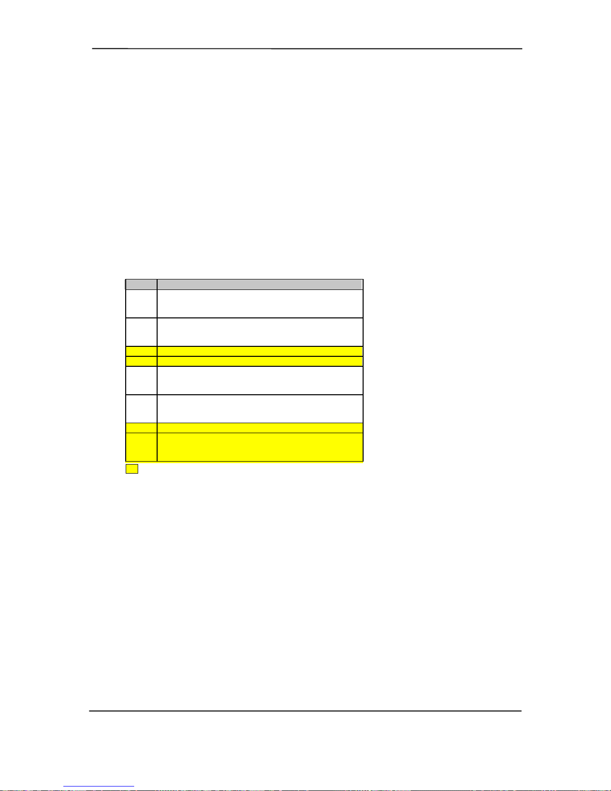
4.3.1.2 Non-Maskable Interrupts
Non-maskable interrupts cannot be masked (inhibited) within the microprocessor itself but may be
maskable by software using logic external to the microprocessor. There are two non-maskable
interrupt signals: the NMI- and the SMI-. These signals have service priority over all maskable
interrupts, with the SMI- having top priority over all interrupts including the NMI-.
NMI- Generation
The Non-Maskable Interrupt (NMI-) signal can be generated by either a parity error detected on a
PCI bus (activating SERR- or PERR-) or by an internal processor error (activating IERRA or
IERRB).
The SERR- and P ERR- signals are rout ed through the ICH c omponent, which in turn activa tes the
NMI to the microprocessor. The NMI Status Register at I/O port 061h contains NMI source and
status data as follows:
NMI Status Register 61h
Bit Function
7 NMI Status:
0 = No NMI from system board pari ty error.
1 = NMI requested, read only
6IOCHK- NMI:
0 = No NMI from IOCHK-
1 = IOCHK- is active (low), NMI requested, read only
5 Interval Timer 1, Counter 2 (Speaker) St atus
4 Refresh Indicator (toggles with every refresh)
3 IOCHK- NMI Enable/Disable:
0 = NMI from IOCHK- enabled
1 = NMI from IOCHK- disabled and c l eared (R/W)
2 System Board Parity Error (P ERR/SERR) NMI Enable:
0 = Parity error NMI enabled
1 = Parity error NMI disabled and cleared (R/W)
1 Speaker Data (R/W)
0 Inteval Timer 1, Counter 2 Gate Signal (R/ W)
0 = Counter 2 disabled
1 = Counter 2 enabled
Functions not related to NMI activity.
Technical Reference Guide
After the active NMI has been processed, status bits <7> or <6> are cleared by pulsing bits <2> or
<3> respectively. The NMI Enable Register (070h, <7>) is used to enable/disable the NMI signal.
Writing 80h to this register masks generation of the NMI-. Note that the lower six bits of register at
I/O port 70h affect RTC operation and should be considered when changing NMI- generation
status.
SMI- Generation
The SMI- (System Management Interrupt) is typically used for power management functions.
When power management is enabled, inactivity timers are monitored. When a timer times out,
SMI- is asserted and invokes the microprocessor’s SMI handler. The SMI- handler works with the
APM BIOS to service the SMI- according to the cause of the timeout. Although the SMI- is
primarily used for power managment the interrupt is also employed for the QuickLock/QuickBlank
functions as well.
Compaq iPAQ Series of Desktop Personal Computers
Second Edition - February 2001
4-9
Page 62

Chapter 4 System Support
4.3.2 DIRECT MEMORY ACCESS
Direct Memory Access (DMA) is a method by which a device accesses system memory without
involving the microprocesso r. Although the DMA method has been traditionally used to transfer
blocks of data to or from an ISA I/O device, PCI devices may also use DMA operation as well.
The DMA method reduces the amount of CPU interactions with memory, freeing the CPU for
other proce ssing tasks.
NOTE: This section describes DMA in general. For detailed information regarding
DMA operation, refer to the data manual fo r the Intel 82801 I/O Controller Hub.
The 82801 component includes the equivalent of two 8237 DMA controllers cascaded together to
provide eight DMA channels, each (excepting channel 4) configurable to a specific device. Table
4-5 lists the default configuration of the DMA channels.
Table 4-5. Default DMA Channel Assignments And Register I/O Port s
DMA Channel Assignments And Register Ports
DMA Channel Function I/O Port
Controller 1 (byte transfers)
0
1
2
3
Controller 2 (word transfers)
4
5
6
7
Refresh 08Fh [see note]
NOTE:
The DMA memory page register for the refresh channel must be
programmed with 00h for proper operation.
Unused
Audio subsystem
Diskette drive
Parallel port (ECP or EPP mode)
Cascade for controller 1
Unused
Unused
Unused
Table 4-5
Control registers 000h-00Eh
Page register 087h
Page register 083h
Page register 081h
Page register 082h
Control registers 0C0h-0DEh
n/a
Page register 08Bh
Page register 089h
Page register 08Ah
All channels in DMA controller 1 operate at a higher priority than those in controller 2. Note that
channel 4 is not available for use other than its cascading function for controller 1. The DMA
controller 2 can transfer words only on an even address boundary. The DMA controller and page
register define a 24-bit address that allows data transfers within the address space of the CPU.
In addition to device configuratio n, each channel can be configured (through PCI Configuration
Registers) for one of two modes of operation:
♦ LPC DMA Mode - Uses the LPC bus to communicate DMA channel control and is
implemented for d evices using DMA through the I/O controller such as the d iskette drive
controller.
♦ PC/PCI DMA Mode - Uses the REQ#/GNT# signals to communicate DMA channel control
and is used by PCI expansion devices.
Compaq iPAQ Series of Desktop Personal Computers
4-10
Second Edition – February 2001
Page 63

4.4 SYSTEM CLOCK DISTRIBUTION
CMOS
These systems use an Intel CK-type clock generator and crystal for generating the clock signals
required by the system board components. Table 4-6 lists the system board clock signals and how
they are distributed.
Table 4-6. Clock Generatio n and Distribution
Table 4-6
Clock Generation and Distribution
Frequncy Source Destination
100 or 133 MHz CK Proc essor, GMCH, DIMM sockets
66 MHz CK GMCH, ICH2, AGP slot
48 MHz CK GMCH, ICH/ICH2, I/O Cntlr.
33 MHz CK Processor, ICH/ICH2, PCI Slots
14.31818 MHz Crystal CK
14.31818 MHz CK ICH/ICH2, I/O Cntlr., and (on iPAQ 2.0) audio codec
Certain clock outputs are turned off during reduced power modes to conserve energy. Clock output
control is handled through the SMBus interface by BIOS.
Technical Reference Guide
4.5 REAL-TIME CLOCK AND CONFIGURATION MEMORY
The Real-time clock (RTC) and configuration memory (also referred to as “CMOS”) functions are
provided by the ICH component and is MC146818-compatible. As shown in the following figure,
the ICH component provides 256 bytes of battery-backed RAM divided into two 128-byte
configuration memory areas. The RTC uses the first 14 bytes (00-0Dh) of the standard memory
area. All locations of the standard memory area (00-7Fh) can be directly accessed using
conventional OUT and IN asse mbl y language instructions thr ough I/O ports 70h/71h, alt hough the
suggested method is to use the INT15 AX=E823h BIOS call.
0Dh
0Ch
0Bh
0Ah
09h
08h
07h
06h
05h
04h
03h
02h
01h
00h
Register D
Register C
Register B
Register A
Date of Month
Day of Week
Hours (Alarm)
Hours (Timer)
Minutes (Alarm)
Minutes (Timer)
Seconds (Alarm)
Seconds (Timer)
Year
Month
82801
Extended Config.
Memory Area
(128 bytes)
Standard Config.
Memory Area
(114 bytes)
RTC Area
(14 bytes)
FFh
80h
7Fh
0Eh
0Dh
00h
Figure 4-5. Configuration Memory Map
A lithium 3-VDC battery is used for maintaining the RTC and configuration memory while the
system is powered down. The battery is located in a battery holder on the system board is replaced
with a Renata CR2032 or equivalent 3-VDC lithium battery.
Compaq iPAQ Series of Desktop Personal Computers
4-11
Second Edition - February 2001
Page 64

Chapter 4 System Support
4.5.1 CLEARING CMOS
NOTE: There is no provision for clearing the contents of CMOS in iPAQ 1.0/1.2
systems. Recovery from a suspected corrupted CMOS is by using the Power Button
Override function as described in section 4.5.2.
The contents of configuration memory (including the Power-On Password) can be cleared on
iPAQ 2.0 systems using the fol l owing procedure:
1. Turn off the unit.
2. Disconnect the AC power cord from the outlet and/or system unit.
3. Remove the chassis hood (cover).
4. Insert a non-metallic object (such as a pencil eraser) through the CMOS clear butto n access
hole and press and release the CMOS clear button.
5. Replace the chassis hood (cover).
6. Reconnect the AC power cord to the outlet and/or system unit.
7. Turn the unit on.
To clear only the Power-On Password refer to section 4.6.1.1.
4.5.2 CMOS ARCHIVE AND RESTORE
On iPAQ 1.0/1.2 systems, the BIOS saves a copy of NVRAM (CMOS contents, password(s) and
other system variables) in a portion of the flash ROM during the boot sequence. Should the system
become un-usable, the last good copy of NVRAM data can be restored with the Power Button
Override function. This func tion is invoked with the following proc edure:
1. With the unit powered down, press and release the power button.
2. Immediately after releasing the power button in step 1, press and hold the power button until
the unit powers down. This action will be recorded as a Power Button Override event.
With the next startup sequence the BIOS will detect the occurrence of the Power Button Override
event and will load the backup copy of NVRAM from the ROM to the CMOS.
NOTE: The Power Button Override feature does not allow quick cycling of the system
(turning on then off). If the power cord is disconnected during the POST routine, the
splash screen image may become corrupted, requiring a re-flashing of the ROM (refer to
chapter 8, BIOS ROM).
Compaq iPAQ Series of Desktop Personal Computers
4-12
Second Edition – February 2001
Page 65

4.5.3 STANDARD CMOS LOCATIONS
Table 4-7 and the following paragraphs describe standard configuration memory locations 0Ah3Fh. These locations are accessible using OUT/IN assembly language instructions using port
70/71h or BIOS function INT15, AX=E823h.
Table 4-7. Configuration Memory (CMOS) Map
Configuration Memory (CMOS) Map
Location Function Location Function
00-0Dh Real -t i me clock 24h System board ID
0Eh Diagnostic status 25h System architecture data
0Fh System reset code 26h Auxiliary peripheral configuration
10h Diskette dri ve t ype 27h Speed control external drive
11h Reserved 28h Expanded/base mem. size, IRQ12
12h Hard drive type 29h Miscellaneous configuration
13h Security func tions 2Ah Hard drive timeout
14h Equipment i nstalled 2Bh Syst em inactivity timeout
15h Base memory size, low byte/KB 2Ch Monitor timeout, Num Lock Cntrl
16h Base memory size, high byte/KB 2Dh Additional flags
17h Extended memory, l ow byte/KB 2Eh-2Fh Checksum of locations 10h-2Dh
18h Extended memory, hi gh byte/KB 30h-31h Total extended memory tested
19h Hard drive 1, primary c ontroller 32h Century
1Ah Hard drive 2, primary c ontroller 33h Miscellaneous flags set by BI OS
1Bh Hard drive 1, secondary c ont rol l e r 34h Internat ional language
1Ch Hard drive 2, secondary controller 35h APM status flags
1Dh Enhanced hard drive support 36h ECC POST test single bit
1Eh Reserved 37h-3Fh Power-on password
1Fh Power management functions 40-FFh Feature Control/Stat us
NOTES:
Assume unmark ed gaps are reserved.
Technical Reference Guide
Table 4-7.
Compaq iPAQ Series of Desktop Personal Computers
4-13
Second Edition - February 2001
Page 66

Chapter 4 System Support
RTC Control Register A, Byte 0Ah
Bit Function
7 Update in Progress. Read only.
0 = Time update will not occur before 2444 us
1 = Time update will occur within 2444 us
6..4 Divider Chain Control. R/W.
00x = Oscillator disabled.
010 = Normal operation (time base frequency = 32.768 KHz).
11x = Divider chain reset.
3..0 Periodic Interrupt Control. R/ W. Specif i es the periodic interrupt interval .
0000 = none 1000 = 3.90625 ms
0001 = 3.90625 ms 1001 = 7.8125 ms
0010 = 7.8125 ms 1010 = 15. 625 ms
0011 = 122.070 us 1011 = 31.25 ms
0100 = 244.141 us 1100 = 62.50 ms
0101 = 488.281 us 1101 = 125 ms
0110 = 976.562 us 1110 = 250 ms
0111 = 1.953125 ms 1111 = 500 ms
RTC Control Register B, Byte 0Bh
Bit Function
7 Time Update Enable/disable
0 = Normal operation, 1 = Disable t i me updating for time set
6 Periodic Interrupt Enable/Disabl e.
0 = Disable, 1 = Enable interval specified by Register A
5 Alarm Interrupt Enable/dis abl e
0 = Disabled, 1 = Enabled
4 End-of-Update Interrupt Enable/Disabl e
0 = Disabled, 1 = Enabled
3 Reserved (read 0)
2 Time/Date Format Select
0 = BCD format, 1 = Binary f ormat
1 Time Mode
0 = 12-hour mode, 1 = 24-hour mode
0 Automatic Daylight Savings Time Enable/Disable
0 = Disable
1 = Enable (Advance 1 hour on 1
October).
st
Sunday in April, retreat 1 hour on las t Sunday in
RTC Status Register C, Byte 0Ch
Bit Function
7 If set, interrupt output signal active (read only)
6 If set, indicates periodi c interrupt flag
5 If set, indicates alarm interrupt
4 If set, indicates end-of-update interrupt
3..0 Reserved
RTC Status Register D, Byte 0Dh
Bit Function
7 RTC Power Status
0 = RTC has lost power
1 = RTC has not lost power
6..0 Reserved
Configuration Byte 0Eh, Diag nostic Status
Default Value = 00h
This byte contai ns diagnostic status d ata.
Compaq iPAQ Series of Desktop Personal Computers
4-14
Second Edition – February 2001
Page 67

Configuration Byte 0Fh, System Reset Code
Default Value = 00h
This byte contains the system reset code.
Configuration Byte 10 h, Diskette Driv e Type
Bit Function
7..4 Primary (Drive A) Disket te Drive Type
3..0 Secondary (Drive B) Diskette Dri ve Type
Valid values for bits <7..4> and bits <3..0>:
0000 = Not installed
0001 = 360-KB drive
0010 = 1.2-MB drive
0011 = 720-KB drive
0100 = 1.44-MB/1.25-MB drive
0110 = 2.88-MB drive
(all other values reserved)
Technical Reference Guide
Configuration Byte 12h, Hard Drive Type
Bit Function
7..4 Primary Controller 1, Hard Drive 1 Type:
0000 = none 1000 = Type 8
0001 = Type 1 1001 = Type 9
0010 = Type 2 1010 = Type 10
0011 = Type 3 1011 = Type 11
0100 = Type 4 1100 = Type 12
0101 = Type 5 1101 = Type 13
0110 = Type 6 1110 = Type 14
0111 = Type 7 1111 = other (use bytes 19h)
3..0 Primary Controller 1, Hard Drive 2 Type:
0000 = none 1000 = Type 8
0001 = Type 1 1001 = Type 9
0010 = Type 2 1010 = Type 10
0011 = Type 3 1011 = Type 11
0100 = Type 4 1100 = Type 12
0101 = Type 5 1101 = Type 13
0110 = Type 6 1110 = Type 14
0111 = Type 7 1111 = other (use bytes 1Ah)
Compaq iPAQ Series of Desktop Personal Computers
4-15
Second Edition - February 2001
Page 68

Chapter 4 System Support
Configuration Byte 13h, Security Functions
Default Value = 00h
Bit Function
7 Reserved
6 QuickBlank Enable After S tandby:
0 = Disable
1 = Enable
5 Administrator Password:
0 = Not present
1 = Present
4 Reserved
3 Diskette Boot Enable:
0 = Enable
1 = Disable
2 QuickLock Enable:
0 = Disable
1 = Enable
1 Network Server Mode/Security Lock Override:
0 = Disable
1 = Enable
0 Password State (Set by BIOS at P ower-up)
0 = Not set
1 = Set
Configuration Byte 1 4h, Equipment Installed
Default Value (standard confi guration) = 03h
Bit Function
7,6 No. of Diskette Drives Installed:
00 = 1 drive 10 = 3 drives
01 = 2 drives 11 = 4 drives
5..2 Reserved
1 Coprocessor Present
0 = Coprocessor not installed
1 = Coprocessor installed
0 Diskette Drives Present
0 = No diskette drives inst al l ed
1 = Diskette drive(s) inst al l ed
Configuration Bytes 15h and 16h, Base Memory Size
Default Value = 280h
Bytes 15h and 16h hold a 16-bit value that specifies the base memory size in 1-KB (1024)
increments. Valid base memory sizes are 512 and 640 kilobytes .
Configuration Bytes 17h and 18h, Extended Memory Size
Bytes 17h and 18h hold a 16-bit value that specifies the extended memory size in 1-KB
increments.
Compaq iPAQ Series of Desktop Personal Computers
4-16
Second Edition – February 2001
Page 69
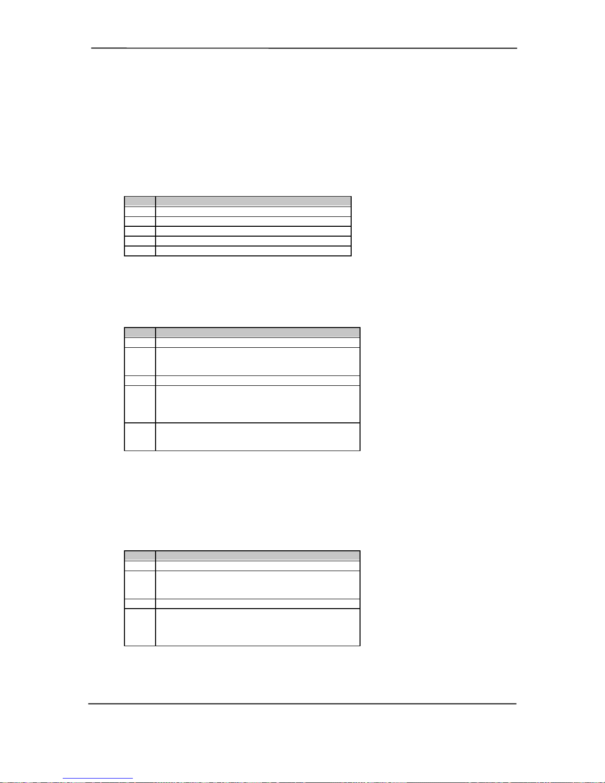
Technical Reference Guide
Configuration Bytes 19 h- 1Ch, Hard Drive Types
Byte 19h contains the hard drive type for drive 1 of the primary controller if byte 12h bits <7..4>
hold 1111b. Byte 1Ah contains the hard drive type for drive 2 of the primary controller if byte 12h
bits <3..0> hold 1111b. Bytes1Bh and 1Ch contain the hard drive types for hard drives 1 and 2 of
the secondary controller.
Configuration Byte 1Dh, Enhanced IDE Hard Drive Support
Default Value = F0h
Bit Function
7 EIDE - Drive C (83h)
6 EIDE - Drive D (82h)
5 EIDE - Drive E (81h)
4 EIDE - Drive F (80h)
3..0 Reserved
Values for bits <7..4> :
0 = Disable
1 = Enable for auto-configure
Configuration Byte 1Fh, Power Management Functions
Default Value = 00h
Bit Function
7..4 Reserved
3 Slow Processor Clock for Low Power Mode
0 = Processor runs at full speed
1 = Processor runs at slow speed
2 Reserved
1 Monitor Off Mode
0 = Turn monitor power off after 45 mi nutes in
standby
1 = Leave monitor power on
0 Energy Saver Mode Indicator (Blinking LED)
0 = Disable
1 = Enable
Configuration Byte 24 h, Sy stem Board Identification
Default Value = 7Eh
Configuration memory location 24h holds the system board ID.
Configuration Byte 25h, System Architecture Data
Default Value = 0Bh
Bit Function
7..4 Reserved
3 Unmapping of ROM:
0 = Allowed
1 = Not allowed
2 Reserved
1,0 Diagnostic Status Byte Address
00 = Memory locations 80C00000h-80C00004h
01 = I/O ports 878h-87Ch
11 = neither place
Compaq iPAQ Series of Desktop Personal Computers
Second Edition - February 2001
4-17
Page 70

Chapter 4 System Support
Configuration Byte 26h, Auxiliary Peripheral Config uration
Default Value = 00h
Bit Function
7,6 I/O Delay Select
00 = 420 ns (default)
01 = 300 ns
10 = 2600 ns
11 = 540 ns
5 Alternative A20 Switching
0 = Disable port 92 mode
1 = Enable port 92 mode
4 Bi-directional Print Port Mode
0 = Disabled
1 = Enabled
3 Graphics Type
0 = Color
1 = Monochrome
2 Hard Drive Primary/Secondary Address Select:
0 = Primary
1 = Secondary
1 Diskette I/O Port
0 = Primary
1 = Secondary
0 Diskette I/O Port Enable
0 = Primary
1 = Secondary
Configuration Byte 27h, Speed Control/External Drive
Default Value = 00h
Bit Function
7 Boot Speed
0 = Max MHz
1 = Fast speed
6..0 Reserved
Configuration Byte 28 h, Expanded and Base Memory, IRQ12 Select
Default Value = 00h
Bit Function
7 IRQ12 Select
0 = Mouse
1 = Expansion bus
6,5 Base Memory Size:
00 = 640 KB
01 = 512 KB
10 = 256 KB
11 = Invalid
4..0 Internal Compaq Memory:
00000 = None
00001 = 512 KB
00010 = 1 MB
00011 = 1.5 MB
.
.
11111 = 15.5 MB
Compaq iPAQ Series of Desktop Personal Computers
4-18
Second Edition – February 2001
Page 71

Configuration Byte 29 h, Miscellaneous Configuration Dat a
Default Value = 00h
Bit Function
7..5 Reserved
4 Primary Hard Drive Enable (Non-PCI IDE Control l ers)
0 = Disable
1 = Enable
3..0 Reserved
Configuration Byte 2Ah, Hard Drive Timeout
Default Value = 02h
Bit Function
7..5 Reserved
4..0 Hard Drive Timeout (index to SIT timeout record)
Configuration Byte 2Bh, System Inactivity Timeout
Default Value = 23h
Bit Function
7 Reserved
6,5 Power Conservation Boot
00 = Reserved
01 = PC on
10 = PC off
11 = Reserved
4..0 System Inactive Timeout. (Index to SIT system timeout
record)
00000 = Disabled
Technical Reference Guide
Configuration Byte 2Ch, ScreenSave and NUMLOCK Control
Default Value = 00h
Bit Function
7 Reserved
6 Numlock Control
0 = Numlock off at power on
1 = Numlock on at power on
5 Screen Blank Control:
0 = No screen blank
1 = Screen blank w/QuickLock
4..0 ScreenSave Timeout. (Index to SIT monitor timeout record)
000000 = Disabled
Compaq iPAQ Series of Desktop Personal Computers
4-19
Second Edition - February 2001
Page 72

Chapter 4 System Support
Configuration Byte 2Dh, Additional Flags
Default Value = 00h
Bit Function
7..5 Reserved
4 Memory Test
0 = Test memory on power up only
1 = Test memory on warm boot
3 POST Error Handling (BIOS Defined)
0 = Display “Press F1 to Continue” on error
1 = Skip F1 message
2..0 Reserved
Configuration Byte 2Eh, 2Fh, Checksum
These bytes hold the checksum of bytes 10h to 2Dh.
Configuration Byte 30h, 31h, Total Extended Memory Tested
This location holds the amount of system memory that checked good during the POST.
Configuration Byte 32h, Cent ury
This location holds the Century value in a binary coded decimal (BCD) format.
Configuration Byte 33h, Miscellaneous Flags
Default Value = 80h
Bit Function
7 Memory Above 640 KB
0 = No, 1 = Yes
6 Reserved
5 Weitek Numeric Coprocessor Present:
0 = Not installed, 1 = Inst all ed
4 Standard Numeric Coprocessor Present:
0 = Not installed, 1 = Inst all ed
3..0 Reserved
Configuration Byte 34h, International Language Support
Default Value = 00h
Compaq iPAQ Series of Desktop Personal Computers
4-20
Second Edition – February 2001
Page 73

Configuration Byte 35h, AP M Status Flags
Default Value = 11h
Bit Function
7..6 Power Conservation State:
00 = Ready
01 = Standby
10 = Suspend
11 = Off
5,4 Reserved
3 32-bit Connection:
0 = Disconnected, 1 = Connected
2 16-bit Connection
0 = Disconnected, 1 = Connected
1 Real Mode Connection
0 = Disconnected, 1 = Connected
0 Power Management Enable:
0 = Disabled
1 = Enabled
Configuration Byte 36h, ECC P OST Test Single Bit Errors
Default Value = 01h
Bit Function
7 Row 7 Error Detect
6 Row 6 Error Detect
5 Row 5 Error Detect
4 Row 4 Error Detect
3 Row 3 Error Detect
2 Row 2 Error Detect
1 Row 1 Error Detect
0 Row 0 Error Detect
0 = No single bit error detected.
1 = Single bit error detected.
Technical Reference Guide
Configuration Byte 37h-3Fh, Power-On Password
These eight locations hold the power-on password.
Compaq iPAQ Series of Desktop Personal Computers
Second Edition - February 2001
4-21
Page 74

Chapter 4 System Support
4.6 SYSTEM MANAGEMENT
This section describes functi ons having to do with secur ity, power management, temperature, and
overall status. These functions are handled by hardware and firmware (BIOS) and generally
configured through the Setup utility.
4.6.1 SECURITY FUNCTIONS
These systems include various features that provide different levels of security. Note that this
subsection describes only the hardware functionality (including that supported by Setup) and
does not describe security features that may be provided by the operating system and application
software.
4.6.1.1 Passwords
CAUTION: Both iPAQ 1.x and 2.0 systems support the use of Setup and Power-On
!
passwords and implement them in the same way. An iPAQ 2.0 system with enabled but
forgotten passwords may be restarted after clearing CMOS with the CMOS clear button
(section 4.5.1). However, the iPAQ 1.0/1.2 does not include a CMOS clear button and
enabling and then forgetting both the Setup and Power-On passwords on an iPAQ 1.0/1.2
system will require invoking a special utility with a service password based on the unit
serial number and date. The utility can be invoked only as a network application
through Compaq Customer Support.
Setup Password
The Setup utility may be configured to be always changeable or changeable only by entering a
password. The password is held on CMOS and if enabled and forgotten, will inhibit any changes
offered by the Setup utility. Refer to the previous Caution for dealing with forgotten passwords.
Power-On Password
These systems support the use of a power-on password, which may be enabled or disabled through
the Setup utility. The password is stored in configuration memory (CMOS). If enabled and then
forgotten on iPAQ 1.0/1.2 systems refer to the previous Caution statement. Forgotten Power-On
passwords for iPAQ 2.0 systems can be cleared using the procedure described below or the entire
CMOS be cleared (refer to section 4.5.1).
To clear only the Power-On password, use the following procedure:
1. Turn off the system and disconnect the AC power cord from the outlet and/or system unit.
2. Remove the cover (hood). Insure that all system board LEDs are off (not illuminated).
3. Locate the password header/jumper (labeled E49 on these systems) and remove the jumper
from pins 1 and 2 and place on (just) pin 2 (for safekeeping).
4. Replace the cover.
5. Re-connect the AC power cord to the AC outlet and/or system unit.
6. Turn on the system. The POST routine will clear and disable the password.
7. To re-enable the password feature, repeat steps 1-6, replacing the jumper on pins 1 and 2 of
header E49.
Compaq iPAQ Series of Desktop Personal Computers
4-22
Second Edition – February 2001
Page 75

DriveLock Password
These systems support the DriveLock security feature for a compatible hard drive installed in the
Multibay. When enabled, DriveLock prevents unauthorized access to hard drive data by requiring
either a master DriveLock or a user DriveLock password to be entered. Although this function is
controlled through the Setup utility, the password information is stored in a reserved area on the
hard drive so that the password(s) will stay or move with the drive.
CAUTION: The DriveLo ck feature is desi gned primarily for business environments
!
where removable hard drives may be moved from system to system. Since forgetting both
DriveLock passwords for a particular drive will result in the data on that drive being no
longer accessible, it is strongly advised that this feature b e invoked and manage d by a
system administrator. For detailed user information consult the appropriate user reference
guide for this system.
4.6.1.2 Cable Lock Provision
These systems include a chassis cutout (on the rear panel) for the attachment of a cable lock
mechanism.
Technical Reference Guide
4.6.1.3 I/O Interface Security
Serial, parallel, and (on iPAQ legacy systems) the USB interfaces may be disabled individually
through the Setup utility (F10) to guard against unauthor ized access to a system. On iPAQ 2.0
systems the NIC interface may also be disabled through Setup.
4.6.2 POWER MANAGEMENT
The iPAQ 2.0 systems provide baseline hardware support of ACPI- and APM-compliant firmware
and software. Key power-consuming components (processor, chipset, I/O controller, and fan) can
be placed into a reduced power mode either automatically or by user control. The system can then
be brought back up (“wake-up”) by events defined by the ACPI specifi cation. The ACPI wake-up
events supported by this system are listed as follows:
ACPI Wake-Up Event System Wakes From
Power Button Suspend or soft-off
RTC Alarm Suspend or soft-off
Wake On LAN (w/NIC) Suspend or soft-off
PME Suspend or soft-off
Serial Port Ring Suspend or soft-of f
USB Suspend only
Keyboard Suspend only
Mouse Suspend only
Compaq iPAQ Series of Desktop Personal Computers
4-23
Second Edition - February 2001
Page 76

Chapter 4 System Support
4.6.3 SYSTEM STATUS
The iPAQ 2.0 systems provide a visual indication of system boot and ROM flash status through the
keyboard LEDs as listed in table 4-8.
NOTE: The LED indications listed in Table 4-8 are valid only for PS/2-type
keyboards. A USB keyboard will not provide LED status for the listed events, although
audible (beep) indications will occur.
Table 4-8. iPAQ 2.0 System Boot/ROM Flash Status LED Indications
IPAQ 2.0 System Boot/ROM Flash Status LED Indications
Event
System memory failure [1] Blinking Off Off
Graphics controller failure [2] Off Blinking Off
System failure prior t o graphi cs cntlr. initiali zat i on [ 3] Off Off Bl i nking
ROMPAQ diskette not present , faulty, or drive prob. On Off Off
Password prompt Off On Off
Invalid ROM detected - flash fai l e d Blinking [4] Blinking [4] Blinking [4]
Keyboard locked in network mode B l i nking [5] Blinking [5] Blinking [5]
Successful boot bl ock ROM flash On [6] On [6] On [6]
NOTES:
[1] Accompanied by 1 short, 2 long audio beeps
[2] Accompanied by 1 l ong, 2 short audio beeps
[3] Accompanied by 2 l ong, 1 short audio beeps
[4] All LEDs will blink in sync twice, accompanied by 1 long and three short audio beeps
[5] LEDs will blink in sequence (NUM Lock, then CA P s Lock, then Scroll Lock)
[6] Accompanied by ri sing audio tone.
Table 4-8.
NUM Lock
LED
CAPs Lock
LED
Scroll Lock
LED
Table 4-9 lists the operation status codes provided by the iPAQ 2.0 power LED on the front of the
chassis.
Table 4-9. System Status LED Indications
Table 4-9.
IPAQ 2.0 System Status LED Indications
System Status Power LED
S0: System on (normal operation) Steady green
S1: Suspend Blinks green @ 1 Hz
S3: Suspend to RAM Blinks green @ 0.5 Hz
S4: Suspend to disk Blinks green @ 0.25 Hz
S5: Soft off Off - clear
Processor not seated Steady red
CPU thermal shutdown Blinks red @ 4 Hz
ROM error Blinks red @ 1 Hz
Power supply crowbar activated B l i nks red @ .5 Hz
System off Off
Compaq iPAQ Series of Desktop Personal Computers
4-24
Second Edition – February 2001
Page 77

4.6.4 TEMPERATURE SENSING AND COOLING
These systems feature a variable-speed fan integrated into the power supply assembly. Fan speed is
determined by the power supply’s internal sensor.
All systems are designed to use a processor with a passive heat sink. The iPAQ 1.0/1.2 system
includes a system board connector for a processor fan, which, if present, operates in tandem with
the power supply fan. The iPAQ 2.0 system does not provide a connector for a heat sink fan and
therefore should not be upgrad ed with a processor using a heat sink-mounted fan (refer to
processor upgrading section 3.2.3.).
NOTE: These systems are designed to provide optimum cooling with the cover in place.
Operating a system with the cover removed may result in a thermal condition of system
board components, including the processor.
Technical Reference Guide
Compaq iPAQ Series of Desktop Personal Computers
4-25
Second Edition - February 2001
Page 78

Chapter 4 System Support
4.7 REGISTER MAP AND MISCELLANEOUS FUNCTIONS
This section contains the system I/O map and information on general-purpose functions of the ICH
and I/O controller.
4.7.1 SYSTEM I/O MAP
Table 4-10 lists the fixed addresses of the input/output (I/O) ports.
Table 4-10. System I/O Map
Table 4-10.
System I/O Map
I/O Port Function
0000..001Fh DMA Controller 1
0020..002Dh Interrupt Control ler 1
002E, 002Fh Index, Data Ports to LPC47B357 I/O Controller (primary)
0030..003Dh Interrupt Control ler
0040..0042h Timer 1
004E, 004Fh Index, Data Ports to LPC47B357 I/O Controller (secondary)
0050..0052h Timer / Counter
0060..0067h Microcont rol l e r, NMI Cont rol l er (alternating addresses)
0070..0077h RTC Controller
0080..0091h DMA Controller
0092h Port A, Fast A20/Reset Generator
0093..009Fh DMA Controller
00A0..00B1h Interrupt Controller 2
00B2h, 00B3h APM Control/Status Ports
00B4..00BDh Interrupt Controller
00C0..00DFh DMA Controller 2
00F0h Coprocessor error register
0170..0177h IDE Cont rol l er 2 (active only if standard I/O s pace is enabled for primary drive)
01F0..01F7h IDE Controller 1 (active only if standard I/O spac e i s enabled for secondary drive)
0278..027Fh Parallel Port (LPT2)
02E8..02EFh Serial Port (COM4)
02F8..02FFh Serial Port (COM2)
0370..0377h Disk ette Drive Controller Secondary Address
0376h IDE Controller 2 (ac tive only if standard I/O space is enabled for primary drive)
0378..037Fh Parallel Port (LPT1)
03B0..03DFh Graphics Controller
03BC..03BEh Parallel Port (LPT3)
03E8..03EFh Serial Port (COM3)
03F0..03F5h Diskette Drive Controller Primary Addresses
03F6h I DE Controller 1 (active only if standard I/O space is enabled for sec . drive)
03F8..03FFh Serial Port (COM1)
04D0, 04D1h Interrupt Controller
0678..067Fh Parallel Port (LPT2)
0778..077Fh Parallel Port (LPT1)
07BC..07BEh Parallel Port (LPT3)
0CF8h PCI Configuration Address (dword access onl y )
0CF9h Reset Control Register
0CFCh PCI Configuration Data (byt e, word, or dword access)
NOTE:
Assume unmark ed gaps are unused, reserved, or used by functions that employ variable I /O
address mapping. Some ranges may include reserved addres ses.
Compaq iPAQ Series of Desktop Personal Computers
4-26
Second Edition – February 2001
Page 79

4.7.2 82801 ICH GENERAL PURPOSE FUNCTIONS
The 82801 ICH2 component includes a number of single and multi-purpose pins available as
general-purpose input/output (GPIO) ports. The GPIO ports are configured (enabled/disabled)
during POST by BIOS through the PCI configuratio n registers of the ICH ’s LPC I/F Bridge
(82801, function 0). The GPIO ports are controlled through 64 bytes of I/O space that is mapped
during POST.
Table 4-11 lists the utilization of the ICH’s GPIO ports.
Table 4-11. 82801 ICH GPIO Register Utilization
Table 4-11.
82801 ICH2 GPIO Register Utilization
GPIO Port # Function Direction
0 PS LED detect I
1NIC REQ5 I
2IRQE- I
3IRQF- I
4 IRQG- I
5 IRQH- I
6 HD LED detect I
7-- NC
8-- NC
11 Multibay device detect I
12 -- NC
13 SMI from I/O I
18 -- NC
19 -- NC
20 -- NC
21 -- NC
22 -- NC
23 -- NC
24 -- NC
25 -- NC
26 -- NC
27 -- NC
28 Password (1 = Enabled, 0 = Disabled) I
NOTE:
NC = not connected (not used).
Technical Reference Guide
Compaq iPAQ Series of Desktop Personal Computers
4-27
Second Edition - February 2001
Page 80

Chapter 4 System Support
4.7.3 I/O CONTROLLER FUNCTIONS
The I/O controller contains various functions such as the keyboard/mouse interfaces, diskette
interface, serial interfaces, and parallel interface. While the control of these interfaces uses
standard AT-type I/O addressing (as described in chapter 5) the configuration of these functions
occurs through indexed ports using PnP protocol. In these systems, hard ware st rapping selects I/O
addresses 02Eh/02Fh at reset as the Index/Data ports for accessing the logical devices within the
I/O contoller. Table 4-12 lists the PnP control registers for the LPC47Bxx7.
Table 4-12 I/O Controller Control Registers
Table 4-12.
I/O Controller Control Registers
Index Function Reset Value
02h Configuration Control 00h
03h Reserved
07h Logical Device (Interf ace) Select:
00h = Diskette Drive I/F
01h = Rsvd
02h = Rsvd
03h = Parallel I/F
04h = Serial I/F (UART 1)
05h = Serial I/F (UART 2)
06h = Rsvd
07h = Keyboard I/F
08h = Rsvd
09h = Rsvd
0Ah = Runtime Reg. (GPIO Confi g.)
0Bh = Rsvd
20h Super I/O ID Register (SI D) 56H
21h Revision -22h Logical Device Power Control 00h
23h Logical Device Power Management 00h
24h PLL / Oscillator Control 04h
25-2Fh Device specific [2] --
NOTES:
Refer to LPC47Bxx7 data sheet for detailed register information.
00h
The configuration registers are accessed through I/O registers 2Eh (index) and 2Fh (data) after the
configuration phase has been activated by writing 55h once to I/O port 2Eh. The BIOS then
initiates each logical device and then deactivates the configuration phase by writing AAh to 2Eh.
Compaq iPAQ Series of Desktop Personal Computers
4-28
Second Edition – February 2001
Page 81

4.7.3.1 LPC47B357 GPIO Utilization
The LPC47B357 I/O Controller (used in iPAQ 2.0 systems) provides 62 general-purpose pins that
can be individually configured for specific purposes. These pins are configured thr ough the
Runtime registers (logical device 0Ah) during the system’s configuration phase of the boot
sequence by the BIOS.
Table 4-13 lists the GPIO registers for the LPC47B357. Note that not all ports are listed as this
table defines only the custom implementation of GPIO ports. Refer to SMC documentation for
standard usage of unlisted GPIO ports.
Table 4-13. LPC47B357 GPIO Register Utilization (Desktop and Minitower only)
LPC47B357 GPIO Port Utilization (iPAQ 2.0 Only)
GPIO Function Direction GPIO Function Direction
10 Board rev 1 I 42 PME- to ICH2 O
11 Board rev 0 I 43 -- NC
12 Multibay power I 44 Hood Lock NC
13 PME- I 45 Hood Unlock NC
14 WOL NC 46 SMI- to ICH2 O
15 System ID 4 [1] I 60 PCI Slot Reset NC
16 Processor Fan sense NC 61 AGP Slot Reset NC
17 LED test O 62 PW R B utton In I
20 Pri. IDE 80-pin Cable Detect I 63 SLP S3 I
21 Sec. IDE 80-pin Cable Detect I 64 SLP S5 I
22 Multibay reset O 65 CPU Changed/Removed [2] O
23 System ID 2 [1] I 66 PWR Button Out O
24 BIOS fail for AOL O 67 PS On (1 = on, 0 = off) O
25 System ID 3 [1] I 70 A20 Gate control O
26 Processor Present I 71 System ID 0 [1] NC
27 -- NC 72 System ID 1 [ 1] NC
30 PS LED Color Grn O 73 -- NC
31 PS LED Blink O 74 -- NC
32 Thermal Trip I 75 PWR GD (to clock chip) NC
33 2 MB Media ID NC 76 FAN OFF- O
34 FWH Wri te Protect O 85 Kybd/Mouse PWR O
35 FWH Reset O 86 S3 3. 3 VDC On O
36 Diskette Motor B NC -- -- -37 Diskette Select B NC -- -- --
NOTE:
NC = Not connected (not used).
[1] System ID (I D4..0) value for these systems = 00111.
[2] If set, will force “Safe B oot” mode.
Technical Reference Guide
Table 4-13.
Compaq iPAQ Series of Desktop Personal Computers
4-29
Second Edition - February 2001
Page 82

Chapter 4 System Support
4.7.3.2 LPC47B357 I/O Controller Miscellaneous Functions
The iPAQ 2.0 systems utilize the following specialized functions built into the LPC 47B357 I/O
Controller:
♦ Power/Hard drive LED control – The I/O controller provides color and blink control for the
front panel LEDs used for indicating system events as listed below:
System Status Power LED HD LED
S0: System on (normal operation) Steady green Green w/HD activity
S1: Suspend Blinks green @ 1 Hz Off
S3: Suspend to RAM Blink s green @ .5 Hz Off
S4: Suspend to disk Blinks green @ 0.25 Hz Off
S5: Soft off Off - clear Off
Processor not seated Steady red Off
CPU thermal shutdown Blinks red @ 4 Hz Off
ROM error Blinks red @ 1 Hz Of f
Power supply crowbar activated Blinks red @ 0.5 Hz Off
System off Off Off
♦ I/O security – The parallel, serial, and diskette interfaces may be disabled individually by
software and the LPC47B357’s disabling register locked. If the disabling register is locked, a
system reset through a cold boot is required to gain access to the disabling (Device Disable)
register.
♦ Processor present/speed detection – One of the battery-back general-purpose inputs (GPI26)
of the LPC47B357 detects if the processor has been remo ved. T he occurrence of this event is
passed to the ICH that will, during the next boot sequence, initiate the speed selection routine
for the processor. The speed selection function replaces the manual DIP switch configuration
procedure required on previous systems.
♦ Legacy/ACPI power button mode control – The LPC47B357 receives the pulse signal from
the system’s power button and produces the PS On signal according to the mode (legacy or
ACPI) selected. Refer to chapter 7 for more information regarding power management.
4.7.4 820802 FWH FUNCTIONS
The 82802 Firmware Hub (FWH) is loaded with Compaq BIOS, which is discussed in Chapter 7.
The FWH component also includes general purpose ports that are utilized on the iPAQ 2.0 as
indicated in the following table:
Table 4-14. 82802 FWH GPIO Register Utilization
82802 FWH GPIO Register Utilization (iPAQ 2.0 Only)
GPIO Port # Function Direction
0 Legacy module detect (0 = ins talled, 1 = not installed) I
1, 3, 4 Not used NC
2 Display cache module det ect I
NOTE:
NC = not connected (not used).
Table 4-14.
Compaq iPAQ Series of Desktop Personal Computers
4-30
Second Edition – February 2001
Page 83

Chapter 5
INPUT/OUTPUT INTERFACES
5. Chapter 5 INPUT/OUTPUT INTERFACES
5.1 INTRODUCTION
This chapter describes the standard (i.e., system board) interfaces that provide input and output
(I/O) porting of data and specifically discusses interfaces that are controlled through I/O-mapped
registers. The following I/O interfaces are covered in this chapter:
♦ Enhanced IDE interface (5.2) page 5-1
♦ Diskette drive interface (5.3) page 5-5
♦ Serial interfaces (5.4) page 5-6
♦ Parallel interface (5.5) page 5-9
♦ Keyboard/pointing device interface (5.6) page 5-15
♦ Universal serial bus interface (5.7) page 5-22
♦ Audio subsystem (5.8) page 5-26
♦ Network support (5.9) page 5-32
Technical Reference Guide
5.2 ENHANCED IDE INTERFACE
The enhanced IDE (EIDE) interface consists of primary and secondary controllers integrated into
the 82801 component of the chipset. The primary IDE controller supports the hard drive while the
secondary controller supports a device installed in the Multibay. Each controller can be configured
independently for the following modes of operation:
♦ Programmed I/O ( PIO) mode – CPU controls drive transactions through standard I/O mapped
registers of the IDE drive.
♦ 8237 DMA mode – CPU offloads drive transactions using DMA protocol with transfer rates
up to 16 MB/s.
♦ Ultra ATA/66 and UATA/100 modes – Preferred bus mastering source-synchronous protocol
providing peak transfer rates of 66 MB/s (iPAQ 1.x) and 100 MB/s (iPAQ 2.0).
5.2.1 IDE PROGRAMMING
The IDE interface is configured as a PCI device during POST and controlled through I/O-mapped
registers at runtime. Hard drives types not found in the ROM’s parameter table are automatically
configured as to (soft)type by DOS as follows:
Primary controller: drive 0, type 65; drive 1, type 66
Secondary controller: drive 0, type 68; drive 1, type 15
Non-DOS (non-Windows) operating systems may require using Setup (F10) for drive
configuration.
Compaq iPAQ Series of Desktop Personal Computers
5-1
Second Edition - February 2001
Page 84

Chapter 5 Input/Output Interfaces
5.2.1.1 IDE Configuration Registers
The IDE controller is configured as a PCI device with bus mastering capability. The PCI
configuration registers for the IDE controller function (PCI device #31, function #1) are listed in
Table 5-1.
Table 5–1. IDE PCI Configur ation Registers
EIDE PCI Configuration Registers (82801, Device 31/Function 1)
PCI Conf.
Addr. Register
00-01h Vender ID 8086h 24-2Bh Reserved 0’s
02-03h Device ID [1] 2C, 2Dh S ubsystem Vender ID 8086h
04-05h PCI Command 0000h 2E, 2Fh Subsystem ID 2411h
06-07h PCI Stat us 0280h 30-3Fh Reserved 0’s
08h Revision ID 00h 40-43h Primary IDE Timing 0000h
09h Programming 80h 44h Secondary IDE Timing 00h
0Ah Sub-Class 01h 48h Sync. DMA Control 00h
0Bh Base Class Code 01h 4A-4Bh Sync. DMA Timing 0000h
0Dh Master Lat ency Timer 0000h 54h EIDE I/O Config.Register 00h
0Eh Header Type 80h F8-FBh Manufacturer’s ID
0F-1Fh Reserved 00h FC-FFh Reserved
20-23h BMIDE Base A ddress 1h -- -- --
NOTE:
Assume unmark ed gaps are reserved and/or not used.
[1] 82801AA ICH = 2411h, 82801BA ICH2 = 244B h
Table 5-1.
Reset
Value
PCI Conf.
Addr. Register
Reset
Value
5.2.1.2 IDE Bus Master Control Registers
The IDE interface can perform PCI bus master operations using the registers listed in Table 5-2.
These registers occupy 16 bytes of variable I/O space set by software and indicated by PCI
configuration register 20h in the previous table.
Table 5–2. IDE Bus Master Control Registers
Table 5-2.
IDE Bus Master Control Registers
I/O Addr.
Offset
00h 1 Bus Master IDE Command (Primary) 00h
02h 1 Bus Master IDE Status (P ri mary) 00h
04h 4 Bus Master IDE Descriptor Poi n t er (Pri.) 0000 0000h
08h 1 Bus Master IDE Command (Secondary) 00h
0Ah 2 Bus Master IDE Status (Secondary) 00h
0Ch 4 Bus Master IDE Descriptor P oi nter (Sec.) 0000 0000h
NOTE:
Size
(Bytes) Register
Unspecified gaps are reserved, will return indeterminat e data, and should not be written to.
Default
Value
5-2 Compaq iPAQ Series of Desktop Personal Computers
Second Edition – February 2001
Page 85

5.2.2 PRIMARY IDE INTERFACE
These systems use a standard 40-pin connector for the primary IDE device that connects (via a
cable) to the hard drive installed in the drive bay. Note that some signals are re-defined for
UATA/33, /66, and /100 modes, which require a special 80-conductor cable (supplied) designed to
reduce cro ss-talk. Device power is supplied thr ough a separate connector.
Figure 5-1. 40-Pin Primary IDE Connector (on system board).
Table 5–3. 40-Pin Primar y IDE Connector Pinout
40-Pin Primary IDE Connector Pinout
Pin Signal Description Pin Signal Description
1 RE S ET- Reset 21 DRQ DMA Request
2 GND Ground 22 GND Ground
3 DD7 Data Bit <7> 23 IOW- I/O Write [1]
4 DD8 Data Bit <8> 24 GND Ground
5 DD6 Data Bit <6> 25 IOR- I/O Read [2]
6 DD9 Data Bit <9> 26 GND Ground
7 DD5 Data Bit <5> 27 IORDY I/O Channel Ready [3]
8 DD10 Data Bit <10> 28 CSEL Cable Select
9 DD4 Data Bit <4> 29 DAK - DMA Acknowledge
10 DD11 Data Bit <11> 30 GND Ground
11 DD3 Data Bit <3> 31 IRQn Interrupt Request [4]
12 DD12 Data Bit <12> 32 IO16- 16-bit I/O
13 DD2 Data Bit <2> 33 DA1 Addres s 1
14 DD13 Data Bit <13> 34 DSKPDIAG Pas s Diagnostics
15 DD1 Data Bit <1> 35 DA0 Addres s 0
16 DD14 Data Bit <14> 36 DA2 Address 2
17 DD0 Data Bit <0> 37 CS0- Chip Select
18 DD15 Data Bit <15> 38 CS1- Chip Select
19 GND Ground 39 HDACTIVE- Drive Active (front panel LED) [5]
20 -- Key 40 GND Ground
NOTES:
[1] On UATA/33, /66, and /100 modes, re-defined as STOP.
[2] On UATA/33, /66 and /100 mode reads, re-defined as DMARDY-.
On UATA/33, /66 and /100 mode writes , re-defined as STROBE.
[3] On UATA/33, /66 and /100 mode reads, re-defined as STROBE-.
On UATA/33, /66 and /100 mode writes , re-defined as DMARDY-.
[4] Primary connector wired to IRQ14, secondary connector wired to I RQ15.
[5] Pin 39 is used for s pi ndl e sync and drive activity (becom es SPSYNC/DACT-)
when synchronous drives are connected.
Technical Reference Guide
Table 5-3.
Compaq iPAQ Series of Desktop Personal Computers
5-3
Second Edition - February 2001
Page 86

Chapter 5 Input/Output Interfaces
5.2.3 SECONDARY IDE INTERFACE
The secondary IDE interface supports the Multibay device, which may be an optical storage device
(CD-ROM, DVD, LS-120) or a second hard drive mounted in a Multibay adapter that in turn is
installed in the Multibay. Both iPAQ 1.x and 2.0 systems provide a 68-pin female connector
(mounted on a Multibay board) that mates with the corresponding male connector of the Multibay
device or adapter.
1
Figure 5-2. 68-Pin Multibay Connector (on Multibay board).
Table 5–4. 68-Pin Multibay Connector Pinout
68-Pin Multibay Connector Pinout
Pin Signal Description Pin Signal Description
1 RST- Reset 2 GND Ground
3 DD7 Drive Data Bit <7> 4 DD8 Drive Data Bit <8>
5 DD6 Drive Data Bit <6> 6 DD9 Drive Data Bit <9>
7 DD5 Drive Data Bit <5> 8 DD10 Drive Data Bit <10>
9 DD4 Drive Data Bit <4> 10 DD11 Drive Data Bit <11>
11 DD3 Drive Data Bit <3> 12 DD12 Drive Data Bit <12>
13 DD2 Drive Data Bit <2> 14 DD13 Drive Data Bit <13>
15 DD1 Drive Data Bit <1> 16 DD14 Drive Data Bit <14>
17 DD0 Drive Data Bit <0> 18 DD15 Drive Data Bit <15>
19 GND Ground 20 (key) No connection
21 DREQ DMA request 22 GND Ground
23 IOW Drive I/O Write 24 GND Ground
25 IOR Drive I/O Read 26 GND Ground
27 IORDY I/O Channel Ready 28 CSEL Cable select
29 DACK DMA Acknowledge 30 GND Ground
31 IRQ Interrupt request 32 GND Ground
33 DA1 Drive address bit <1> 34 PDIAG Passed diagnostics
35 DA0 Drive address bit <0> 36 DA2 Drive address bit <2>
37 CS1 Chip select 1 38 CS3 Chip select 3
39 DASP- Drive activity/drive 1 prsnt. 40 GND Ground
41 Vcc + 5 V DC l ogi c power 42 MTR PWR +5 VDC m otor power
43 GND Ground 44 AUD L Left audio
45 GND Left audio ground 46 GND Right audio ground
47 AUD R Right audio 48 INDEX- Index
49 Vcc +5 VDC 50 DRVSEL Drive select
51 DSKCHG Disk change 52 GND Ground
53 DEN ID Media identif i cation 54 MTR O N - Motor On
55 LOWDEN- Density select 56 DIR- Direction in
57 STEP- Step 58 DEV PRST System device present
59 WDATA- Write dat a 60 GND Ground
61 WGATE- Write gate 62 TRK0- Track 00
63 GND Ground 64 WPROT- Write protect
65 GND Ground 66 RDATA- Read data
67 GND Ground 68 HDSEL- Head (side one) select
Diskette drive interface not connected.
Table 5-4.
5-4 Compaq iPAQ Series of Desktop Personal Computers
Second Edition – February 2001
Page 87

5.3 DISKETTE DRIVE INTERFACE
NOTE: The Compaq iPAQ does not support a diskette drive. However, the I/O
controller component contains a diskette drive controller that may need to be enabled
(though Setup) to satisfy the requirements of some o perating systems. This may result in
device manager applications indicating the presence of a diskette drive that in fact is not
available.
Technical Reference Guide
Compaq iPAQ Series of Desktop Personal Computers
5-5
Second Edition - February 2001
Page 88

Chapter 5 Input/Output Interfaces
5.4 SERIAL INTERFACE
The legacy models include a serial interface to transmit and receive asynchronous serial data with
external devices. The serial interface function is provided by the I/O controller component that
includes a NS16C550-compatible UART.
NOTE: Legacy-free models do not have an externally accessible serial port, but do have
serial interface logic to satisfy the serial port requirements of some operating systems.
The iPAQ2.0 and legacy-free iPAQ 1.x systems also includes a serial test header on the
system board.
The UART supports the standard baud rates up through 115200, and also special high speed rates
of 239400 and 460800 baud. The baud rate of the UART is typically set to match the capability of
the connected device. While most baud rates may be set at runtime, baud rates 230400 and
460800 must be set during the configuration phase.
5.4.1 RS-232 INTERFACE
On the legacy system, the UART is associated with a DB-9 connector that complies with EIA
standard RS-232-C. The DB-9 connector is shown in the following figure and the pinout of the
connector is listed in Table 5-5.
Figure 5-3. Serial Interface Connector (Male DB-9 as viewed from rear of chassis)
Table 5–5. DB-9 Serial Connector Pinout
Table 5-5.
DB-9 Serial Connector Pinout
Pin Signal Description Pin Signal Description
1 CD Carrier Detect 6 DSR Data S et Ready
2 RX Data Recei ve Dat a 7 RTS Request To Send
3 TX Data Transmit Data 8 CTS Clear To Send
4 DTR Data Terminal Ready 9 RI Ring Indicator
5 GND Ground -- -- --
The standard RS-232-C limitation of 50 feet (or less) of cable between the DTE (computer) and
DCE (modem) should be followed to minimize transmission errors. Higher baud rates may require
shorter cables.
5-6 Compaq iPAQ Series of Desktop Personal Computers
Second Edition – February 2001
Page 89

5.4.2 SERIAL TEST INTERFACE
iPAQ 1.x legacy-free and iPAQ 2.0 systems include a serial header connector on the system board
to satisfy the requirements of some operating systems. The test header and pinout is shown in the
following figure:
Technical Reference Guide
CD 1
RX Data 3
TX Data 5
DTR 7
Gnd 9
Figure 5-4. Serial Interface Header (iPAQ 1.2 legacy-free and 2.0 system boards only)
5.4.3 SERIAL INTERFACE PROGRAMMING
Programming the serial interfaces consists of configuration, which occurs during POST, and
control, which o ccurs during runtime.
5.4.3.1 Serial Interface Configuration
The serial interface must be configured for a specific address range (COM1, COM2, etc.) and also
must be activated before it can be used. Address selection and activation of the serial interface are
affected through the PnP co nfi guration registe rs of the LPC47 B277 I/O controller.
The serial interface configuration registers are listed in the following table:
2 DSR
4 RTS
6 CTS
8 RI
Table 5–6. Serial Interface Configuration Registers
Table 5-6.
Serial Interface Configuration Registers
Index
Address Function R/W
30h Activate R/W
60h Base Address MSB R/W
61h Base Address LSB R/W
70h Interrupt Select R/W
F0h Mode Register R/W
NOTE:
Refer to LPC47B277 data sheet for detailed register informat i on.
5.4.3.2 Serial Interface Control
The BIOS function INT 14 provides basic control of the serial interface. The serial interface can
be directl y controlled by software through the I/O-mapp ed registers list ed in Table 5-7.
Compaq iPAQ Series of Desktop Personal Computers
Second Edition - February 2001
5-7
Page 90

Chapter 5 Input/Output Interfaces
Table 5–7. Serial Interface Control Registers
COM1
Addr.
3F8h 2F8h Receive Data Buffer
3F9h 2F9h Baud Rate Divisor Register 1 (when bit 7 of Line Control Reg. Is set)
3FAh 2FAh Interrupt ID Regis ter:
3FBh 2FBh Line Control Regist er:
3FCh 2FCh Modem Control Register:
3FDh 2FDh Line S tatus Register:
3FEh 2FEh Modem Status :
COM2
Addr. Register R/W
Transmit Data Buffer
Baud Rate Divisor Register 0 (when bit 7 of Li ne Control Reg. Is set)
Interrupt Enable Register:
<7..4> Reserved (always 0’s)
<3> Modem status interrupt enabl e (active high) (CTS, DSR, RI, CD)
<2> Rx line status interrupt enable (active high) (Overrun, parity, framing error)
<1> Tx holding register empty interrupt enable (active high)
<0> Baud rate divisor interrupt enable (ac t i ve hi gh)
<7,6> FIFO Enable/Disable: 0 = dis abl e, 1 = enabl e
<5,4> Reserved
<3..1> Interrupt Source:
000 = Modem status 100,101 = Reserved
001 = TX holding reg. Empty 110 = Character time-out
010 = RX data available 111 = Reserved
011 = RX line status
<0> Interrupt pending (if cleared)
FIFO Control Register:
<7,6> RX Trigger Level: 00 = 1 byte, 01 = 4 bytes, 10 = 8 bytes, 11 = 14 bytes
<5..3> Rerserved
<2> TX FIFO reset (active high)
<1> RX FIFO reset (active high)
<0> FIFO Enable/Disable: 0 = Disable TX/RX FIFO’s, 1 = Enable TX/RX FIFO’s
<7> Register acces control :
0 = RX buffer, TX holding, divisor rate registers are accessable.
1 = Divisor rate register is accessable
<6> Break control (forces S OUT singla low if set)
<5> Stick parity (if set, even parity bit is 0, odd pari ty bit is 1)
<4> Parity type: 0 = odd, 1 = even
<3> Parity enable: 0 = disabled, 1 = enabled
<2> Stop bit: 0 = 1 stop bit, 1 = 2 stop bits
<1,0> Word size: 00 = 5 bi t s, 01 = 6 bits, 10 = 7 bits, 11 = 8 bi ts
<7..5> Reserved
<4> Internal loopback enabled (if s et )
<3> Serial I/F interrupts enabl ed (i f set)
<2> Reserved
<1> RTS signal active (if set)
<0> DTR signal active (if set )
<7> Parity error, framing error, or B reak condition (if set)
<6> TX holding and TX shift registers are empty (if set)
<5> TX holding register is empty (if set)
<4> Break interrupt has occurred (if set)
<3> Framing error has occurred (if s et)
<2> Parity error has occurred (if set)
<1> Overrun error has occurred (if set)
<0> Data register ready to be read (if set )
<7..4> DCD-, RI-, DSR, CTS (respectively) active (if set)
<3..0> DCD-, RI-, DSR, CTS (respectively) changed state s i nce last read (if set)
Table 5-7.
Serial Interface Control Registers
R
W
W
W
R/W
R
W
R/W
R/W
R
R
5-8 Compaq iPAQ Series of Desktop Personal Computers
Second Edition – February 2001
Page 91

5.5 PARALLEL INTERFACE
The legacy models include a parallel interface for connection to a peripheral device that has a
compatible interface, the most common being a printer. The parallel interface function is integrated
into the I/O controller component and provides bi-directional 8-bit parallel data transfers with a
peripheral device. The parallel interface supports three main modes of operation:
♦ Standard Parallel Port (SPP) mode
♦ Enhanced Parallel Port (EPP) mode
♦ Extended Capabilities Port (ECP) mode
These three modes (and their submodes) provide complete support as specified for an IEEE 1284
parallel port.
5.5.1 STANDARD PARALLEL PORT MODE
The Standard Parallel Port (SPP) mode uses software-based protocol and includes two sub-modes
of operation, compatible and extended, both of which can provide data transfers up to 150 KB/s. In
the compatible mode, CPU write data is simply presented on the eight data lines. A CPU read of
the parallel port yields the last data byte that was written. The following steps define the standard
procedure for communicating with a printing device:
Technical Reference Guide
1. The system checks the Printer Status register. If the Busy, Paper Out, or Printer Fault signals
are indicated as being active, the system either waits for a status change or generates an error
message.
2. The system sends a byte of data to the Printer Data register, then pulses the printer STROBE
signal (through the Printer Contr ol register) for at least 500 ns.
3. The system then monitors the Printer Status register for acknowledgment of the data byte
before send ing the next byte.
In extended mode, a direction control bit (CTR 37Ah, bit <5>) controls the latching of output data
while allowing a CPU read to fetch data present on the data lines, thereby providing bi-directional
parallel transfers to occur. The SPP mode uses three registers for operation: the Data register
(DTR), the Status register (STR) and the Control register (CTR). Address decoding in SPP mode
includes address lines A0 and A1.
5.5.2 ENHANCED PARALLEL PORT MODE
In Enhanced Parallel Port (EPP) mode, increased data transfers are possible (up to 2 MB/s) due to
a hardware protocol that provides automatic address and strobe generation. EPP revisions 1.7 and
1.9 are both supported. For the parallel interface to be initialized for EPP mode, a negotiation
phase is entered to detect whether or not the connected peripheral is compatible with EPP mode. If
compatible, then EPP mode can be used. In EPP mode, system timing is closely coupled to EPP
timing. A watchdog timer is used to prevent system lockup. Five additional registers are available
in EPP mode to handle 16- and 32-bit CPU accesses with the parallel interface. Address decoding
includes address lines A0, A1, and A2.
Compaq iPAQ Series of Desktop Personal Computers
5-9
Second Edition - February 2001
Page 92

Chapter 5 Input/Output Interfaces
5.5.3 EXTENDED CAPABILITIES PORT MODE
The Extended Capabilities Port (ECP) mode, like EPP, also uses a hardware protocol-based design
that supports transfers up to 2 MB/s. Automatic generation of addresses and strobes as well as Run
Length Encoding (RLE) decompression is supported by ECP mode. The ECP mode includes a bidirectional FIFO buffer that can be accessed by the CPU using DMA or programmed I/O. For the
parallel interface to be initialized for ECP mode, a negotiation phase is entered to detect whether
or not the connected peripheral is compatible with ECP mode. If compatible, then ECP mode can
be used.
Ten control registers are available in ECP mode to handle transfer operations. In accessing the
control registers, the base address is determined by address lines A2-A9, with lines A0, A1, and
A10 defining the offset address of the control register. Registers used for FIFO operations are
accessed at their base address + 400h (i.e., if configured for LPT1, then 378h + 400h = 778h).
The ECP mode includes several sub-modes as determined by the Extended Control register. Two
submodes of ECP allow the parallel port to be controlled by software. In these modes, the FIFO is
cleared and not used, and DMA and RLE are inhibited.
5.5.4 PARALLEL INTERFACE PROGRAMMING
Programming the parallel interface consists of configuration, which typically occurs during POST,
and contro l , which occurs during runtime.
5.5.4.1 Parallel Interface Configuration
The parallel interface must be configured for a specific address range (LPT1, LPT2, etc.) and also
must be enabled before it can be used. When configured for EPP or ECP mode, additional
considerations must be taken into account. Address selection, enabling, and EPP/ECP mode
parameters of the parallel interface are affected through the PnP configuratio n registers of the
LPC47B347 I/O controller. Address selection and enabling are automatically done by the BIOS
during POST but can also be accomplished with the Setup utility and other software.
The parallel interface configuration registers are listed in the following table:
Table 5–8. Parallel Interface Configuration Registers
Table 5-8.
Parallel Interface Configuration Registers
Index
Address Function R/W
30h Activate R/W 00h
60h Base Address MSB R/W 00h
61h Base Address LSB R/W 00h
70h Interrupt Select R/W 00h
74h DMA Channel Select R/W 04h
F0h Mode Register R/W 00h
F1h Mode Register 2 R/W 00h
Reset
Value
5-10 Compaq iPAQ Series of Desktop Personal Computers
Second Edition – February 2001
Page 93

5.5.4.2 Parallel Interface Control
The BIOS function INT 17 provides simplified control of the parallel interface. Basic functions
such as initialization, character printing, and printer status are provide by subfunctions of INT 17.
The parallel interface is controllable by software through a set of I/O mapped re gisters. The
number and type of registers available depends on the mode used (SPP, EPP, or ECP). Table 5-9
lists the parallel registers and associated functions based on mode.
Table 5–9. Parallel Interface Control Registers
Parallel Interface Control Registers
I/O
Address Register
Base Data LPT1,2,3 LPT1,2 LPT1,2,3
Base + 1h Printer Status LPT1,2,3 LP T1,2 LPT1,2,3
Base + 2h Control LPT1,2,3 LPT1,2 LPT1, 2,3
Base + 3h Address -- LPT1,2 -Base + 4h Data Port 0 -- LPT1,2 -Base + 5h Data Port 1 -- LPT1,2 -Base + 6h Data Port 2 -- LPT1,2 -Base + 7h Data Port 3 -- LPT1,2 -Base + 400h Parallel Data FIFO -- -- LP T1, 2,3
Base + 400h ECP Data FIFO -- -- LPT1,2,3
Base + 400h Test FIFO -- -- LPT1,2,3
Base + 400h Configuration Register A -- -- LPT1,2,3
Base + 401h Configuration Register B -- -- LPT1,2,3
Base + 402h Extended Control Regist er -- -- LPT1,2,3
Table 5-9.
Technical Reference Guide
SPP
Mode
Ports
EPP
Mode
Ports
ECP
Mode
Ports
Base Address:
LPT1 = 378h
LPT2 = 278h
LPT3 = 3BCh
The following paragraphs describe the individual registers. Note that only the LPT1-based
addresses are given in these descriptions.
Data Register, I/O Port 378h
Data written to this register is presented to the data lines D0-D7. A read of this register when in
SPP-compatible mode yields the last byte written. A read while in SPP-extended or ECP mode
yields the status of data lines D0-D7 (i.e., receive data).
In ECP mode in the forward (output) direction, a write to this location places a tagged command
byte into the FIFO and reads have no effect.
Compaq iPAQ Series of Desktop Personal Computers
5-11
Second Edition - February 2001
Page 94

Chapter 5 Input/Output Interfaces
Status Register, I/O Port 379h, Read Only
This register contains the current printer status. Reading this register clears the interrupt condition
of the parallel port.
Bit Function
7 Printer Busy (if 0)
6 Printer Acknowledgment Of Data Byt e (i f 0)
5 Printer Out Of Paper (if 1)
4 Printer Selected/Online (if 1)
3 Printer Error (if 0)
2 Reserved
1 EPP Interrupt Occurred (if set while in EPP mode)
0 EPP Timeout Occurred (if set while in EPP mode)
Control Register, I/O Port 37Ah
This register provides the printer control functions.
Bit Function
7,6 Reserved
5 Direction Control for PS/2 and ECP Modes:
0 = Forward. Drivers enabled. Port writes to peripheral (defaul t)
1 = Backward. Tristates drivers and dat a i s read from peripheral
4 Acknowledge Interrupt Enable
0 = Disable ACK interrupt
1 = Enable interrupt on rising edge of ACK
3 Printer Select (if 0)
2 Printer Initialize (if 1)
1 Printer Auto Line Feed (if 0)
0 Printer Strobe (if 0)
Address Register, I/O Port 37Bh (EPP Mode Only)
This register is used for selecting the EPP register to be accessed.
Data Port Registers 0-3, I/O Ports 37C-Fh (EPP Mode Only)
These registers are used for reading/writing data. Port 0 is used for all transfers. Ports 1-3 are used
for transferring the ad ditional bytes of 16- or 32-bit transfers through por t 0.
FIFO Register, I/O Port 7F8h (ECP Mode Only)
While in ECP/forward mode, this location is used for filling the 16-byte FIFO with data bytes.
Reads have no effect (except when used in Test mode). While in ECP/backward mode, reads
yield data bytes from the FIFO.
5-12 Compaq iPAQ Series of Desktop Personal Computers
Second Edition – February 2001
Page 95

Technical Reference Guide
Configuration Register A, I/O Port 7F8h (ECP Mode Only)
A read of this location yields 10h, while writes have no effect.
Configuration Register B, I/O Port 7F9h (ECP Mode, Read Only)
A read of this location yields the status defined as follows:
Bit Function
7 Reserved (always 0)
6
Status of Select ed I RQn.
5,4 Selected IRQ Indicator:
00 = IRQ7
11 = IRQ5
All other values invalid.
3 Reserved (always 1)
2..0 Reserved (always 000)
Extended Control Register B, I/O Port 7FAh (ECP ModeOnly)
This register defines the ECP mode functions.
Bit Function
7..5 ECP Submode Select:
000 = Standard forward mode (37Ah <5> forced to 0). Writes are
controlled by software and FIFO is reset .
001 = PS/2 mode. Reads and writes are software controlled and
FIFO is reset.
010 = Parallel Port FIFO forward mode (37Ah <5> forc ed to 0). Writes
are
hardware controlled.
011 = ECP FIFO mode. Directi on determined by 37Ah, <5>. Reads and
writes are hardware controlled.
4 ECP Interrupt Mask:
0 = Interrupt is generated on ERR- ass ertion.
1 = Interrupt is inhibited.
3 ECP DMA Enable/Disable.
0 = Disabled
1 = Enabled
2 ECP Interrupt Generation with DMA
0 = Enabled
1 = Disabled
1 FIFO Full Status (Read Only)
0 = Not full (at least 1 empty byte)
1 = Full
0 FIFO Empty Status (Read Onl y)
0 = Not empty (contains at least 1 byte)
1 = Empty
Compaq iPAQ Series of Desktop Personal Computers
5-13
Second Edition - February 2001
Page 96

Chapter 5 Input/Output Interfaces
5.5.5 PARALLEL INTERFACE CONNECTOR
Figure 5-5 and Table 5-10 show the connector and pinout of the parallel interface connector. Note
that some signals are redefined depending on the port’s operational mode.
13 12 11 10 9 8 7 6 5
25 24 23 22 21 20 19 18 17 16 15 14
4
3 2 1
Figure 5-5. Parallel Interface Connector (Female DB-25 as viewed from rear of chassis)
Table 5–10. DB-25 Parallel Connector Pinout
Table 5-10.
DB-25 Parallel Connector Pinout
Pin Signal Function Pin Signal Function
1 STB - Strobe / Write [ 1] 14 LF- Line Feed [2]
2 D0 Data 0 15 ERR- Error [3]
3 D1 Data 1 16 INIT- Initial ize P aper [4]
4 D2 Data 2 17 SLCTIN- Select In / Address. Strobe [1]
5 D3 Data 3 18 GND Ground
6 D4 Data 4 19 GND Ground
7 D5 Data 5 20 GND Ground
8 D6 Data 6 21 GND Ground
9 D7 Data 7 22 GND Ground
10 ACK- Acknowledge / Interrupt [1] 23 GND Ground
11 BSY Busy / Wai t [1] 24 GND Ground
12 PE Paper End / User defined [1] 25 GND Ground
13 SLCT Select / User defined [1] -- -- --
NOTES:
[1] Standard and ECP mode f unction / EPP mode function
[2] EPP mode function: Data Strobe
ECP modes: Auto Feed or Hos t Acknowledge
[3] EPP mode: user defined
ECP modes:Fault or P e ri pheral Req.
[4] EPP mode: Reset
ECP modes: Init i a l i ze or Revers e Req.
5-14 Compaq iPAQ Series of Desktop Personal Computers
Second Edition – February 2001
Page 97

5.6 KEYBOARD/POINTING DEVICE INTERFACE
The legacy models include PS/2-type keyboard/pointing device interfaces for the connection of a
standard enhanced keyboard and a mouse. (Legacy-free models use USB ports for keyboard/mouse
connections.) The keyboard/pointing device interface function is provided by the I/O controller
component, which integrates 8042-compatible keyboard controller logic (hereafter referred to as
simply the “8042”) to communicate with the keyboard and pointing device using bi-directional
serial data transfers. The 8042 handles scan code translation and password lock protection for the
keyboard as well as communications with the pointing device. This section describes the interface
itself. The keyboard is discussed in the Appendix C.
5.6.1 KEYBOARD INTERFACE OPERATION
The data/clock link between the 8042 and the keyboard is uni-directional for Keyboard Mode 1
and bi-directional for Keyboard Modes 2 and 3. (These modes are discussed in detail in Appendix
C). This section describes Mode 2 (the default) mode of operation.
Communication between the keyboard and the 8042 consists of commands (originated by either
the keyboard or the 8042) and scan codes from the keyboard. A command can request an action or
indicate status. The keyboard interface uses IRQ1 to get the attention of the CPU.
Technical Reference Guide
The 8042 can send a command to the keyboard at any time. When the 8042 wants to send a
command, the 8042 clamps the clock signal from the keyboard for a minimum of 60 us. If the
keyboard is transmitting data at that time, the transmission is allowed to finish. When the 8042 is
ready to transmit to the keyboard, the 8042 pulls the data line low, causing the keyboard to
respond by pulling the clock line low as well, allowing the start bit to be clocked out of the 8042.
The data is then transferred serially, LSb first, to the keyboard (Figure 5-6). An odd parity bit is
sent following the eighth data bit. After the parity bit is received, the keyboard pulls the data line
low and clocks this condition to the 8042. When the keyboard receives the stop bit, the clock line
is pulled low to inhibit the keyboard and allow it to process the data.
Data
Clock
Start
BitD0(LSb)
01011011110
Th
D1 D2 D3 D4 D5 D6
Tcl TchTcy Tss Tsh
Parameter Minimum
Tcy (Cycle Time) 0 us 80 us
Tcl (Clock Low) 25 us 35 us
Tch (Clock High) 25 us 45 us
Th (Data Hold) 0 us 25 us
Tss (Stop Bit Setup) 8 us 20 us
Tsh (Stop Bit Hold) 15 us 25 us
Maximum
D7
(MSb)
Parity
Stop
Bit
Figure 5-6. 8042-To-Keyboard Transmission of Code EDh, Timing Diagram
Compaq iPAQ Series of Desktop Personal Computers
5-15
Second Edition - February 2001
Page 98

Chapter 5 Input/Output Interfaces
Control of the data and clock signals is shared by the 8042and the keyboard depending on the
originator of the transferred data. Note that the clock signal is always generated by the keyboard.
After the keyboard receives a command from the 8042, the keyboard returns an ACK code. If a
parity error or timeout occurs, a Resend command is sent to the 8042. Table 5-11 lists and
describes commands that can be issued by the 8042 to the keyboard.
Table 5–11. 8042-To-Keyboard Commands
Command Value Description
Set/Reset Status Indicators EDh Enables LED indicators. Value EDh is followed by an
Echo EEh Keyboard returns EEh when previously enabled.
Invalid Command E Fh/F1hThese commands are not acknowledged.
Table 5-11.
8042-To-Keyboard Commands
option byte that specif i es the indicator as follows:
Bits <7..3> not used
Bit <2>, Caps Lock (0 = off, 1 = on)
Bit <1>, NUM Lock (0 = off, 1 = on)
Bit <0>, Scroll Lock (0 = off, 1 = on)
Select Alternate Scan Codes F0h I nstructs the keyboard to s el ect another set of scan c odes
Read ID F2h Ins tructs the keyboard to stop scanning and return two
Set Typematic Rate/ Di splay F3h Instructs the keyboard t o change typematic rate and delay
Enable F4h Instructs keyboard to clear output buffer and las t
Default Disable F5h Resets keyboard to power-on default s tate and halts
Set Default F6h Resets keyboard t o power-on default state and enable
Set Keys - Typematic F7h Clears keyboard buffer and sets default scan code set. [1]
Set Keys - Make/Brake F8h Clears keyboard buffer and sets defaul t scan code set. [1]
Set Keys - Make F9h Clears keyboard buff er and sets default scan c ode set. [1]
Set Keys - Typematic/Make/Brake FAh Clears k eyboard buffer and sets default s can code set. [1]
Set Type Key - Typematic FBh Clears keyboard buffer and prepares to receive key ID. [1]
Set Type Key - Make/Brake FCh Clears keyboard buffer and prepares t o receive key ID. [1]
Set Type Key - Make FDh Clears keyboard buffer and prepares to receive key ID. [1]
Resend FEh 8042 detected error in keyboard transmission.
Reset FFh Resets program, runs keyboard BAT, defaults to Mode 2.
Note:
[1] Used in Mode 3 only.
and sends an option byte after ACK i s received:
01h = Mode 1
02h = Mode 2
03h = Mode 3
keyboard ID bytes.
to specified values:
Bit <7>, Reserved - 0
Bits <6,5>, Delay Time
00 = 250 ms
01 = 500 ms
10 = 750 ms
11 = 1000 ms
Bits <4..0>, Transmission Rate:
00000 = 30.0 ms
00001 = 26.6 ms
00010 = 24.0 ms
00011 = 21.8 ms
:
11111 = 2.0 ms
typematic key and begin k e y scanning.
scanning pending next 8042 command.
scanning.
5-16 Compaq iPAQ Series of Desktop Personal Computers
Second Edition – February 2001
Page 99

Technical Reference Guide
5.6.2 POINTING DEVICE INTERFACE OPERATION
The pointing device (typically a mouse) connects to a 6-pin DIN-type connector that is identical to
the keyboard connector both physically and electrically. The operation of the interface (clock and
data signal control) is the same as for the keyboard. The pointing device interface uses the IRQ12
interrupt.
5.6.3 KEYBOARD/POINTING DEVICE INTERFACE PROGRAMMING
Programming the keyboard interface consists of configuration, which occurs during POST, and
control, which o ccurs during runtime.
5.6.3.1 8042 Configuration
The keyboard/pointing device interface must be enabled and configured for a particular speed
before it can be used. Enabling and speed parameters of the 8042 logic are affected through the
PnP configuration registers of the LPC47B347 I/O controller. Enabling and speed control are
automatically set by the BIOS during POST but can also be accomplished with the Setup utility
and other software.
The keyboard interface configuration registers are listed in the following table:
Table 5–12. Keyboard Interface Configuration Registers
Table 5-12.
Keyboard Interface Configuration Registers
Index
Address Function R/W
30h Activate R/W
70h Primary Interrupt S el ect R/W
72h Secondary Interrupt Selec t R/W
F0h Reset and A 20 S el ect R/W
Compaq iPAQ Series of Desktop Personal Computers
5-17
Second Edition - February 2001
Page 100

Chapter 5 Input/Output Interfaces
5.6.3.2 8042 Control
The BIOS function INT 16 is typically used for controlling interaction with the keyboard. Subfunctions of INT 16 conduct the basic routi nes of handling keyboard data (i. e., translating the
keyboard’s scan codes into ASCII codes). The keyboard/pointing device interface is accessed by
the CPU through I/O mapped ports 60h and 64h, which provide the following functions:
♦ Output buffer reads
♦ Input buffer writes
♦ Status reads
♦ Command writes
Ports 60h and 64h can be accessed using the IN instruction for a read and the OUT instruction for
a write. Prior to reading data from port 60h, the “Output Buffer Full” status bit (64h, bit <0>)
should be checked to ensure data is available. Likewise, before writing a command or data, the
“Input Buffer Empty” status bit (64h, bit <1>) should also be checked to ensure space is available.
I/O Port 60h
I/O port 60h is used for accessing the input and output buffers. This register is used to send and
receive data from the keyboard and the pointing device. This register is also used to send the
second byte of multi-byte commands to the 8042 and to receive responses from the 8042 for
commands that require a response.
A read of 60h by the CPU yields the byte held in the output buffer. The output buffer holds data
that has been received from the keyboard and is to be transferred to the system.
A CPU write to 60h places a data byte in the input byte buffer and sets the CMD/ DATA bit of the
Status register to DATA. The input buffer is used for transferring data from the system to the
keyboard. All data written to this port by the CPU will be transferred to the keyboard except bytes
that follow a multibyte command that was written to 64h
I/O Port 64h
I/O port 64h is used for reading the status register and for writing commands. A read of 64h by the
CPU will yield the status byte defined as follows:
Bit Function
7..4 General Purpose Flags.
3 CMD/DATA Flag (reflects the stat e of A2 during a CPU
write).
0 = Data
1 = Command
2 General Purpose Flag.
1 Input Buffer Full. Set (to 1) upon a CP U write. Cleared by
IN A, DBB instruction.
0 Output Buffer Full (if set). Cleared by a CPU read of the
buffer.
A CPU write to I/O port 64h places a command value into the input buffer and sets the
CMD/DATA bit of the status register (bit <3>) to CMD.
5-18 Compaq iPAQ Series of Desktop Personal Computers
Second Edition – February 2001
 Loading...