

Page 1

HF SSB Transceiver
9323, 9360, 9390 and 9780
Technical Service Manual
No part of this handbook may be reproduced, transcribed, translated into any
language or transmitted in any form whatsoever without the prior written consent
of Codan Pty Ltd
1994 Codan Pty Ltd.
Codan part number 15-02051 Issue 4, August 1997
Page 2

Head Office
Codan Pty Ltd
ACN 007 590 605
81 Graves Street
Newton
South Australia 5074
Telephone +61 8 8305 0311
Facsimile +61 8 8305 0411
Email
Worldwide Web
http://www.codan.com.au
Marketing Offices
Codan Pty Ltd
Suite 11A
2 Hardy Street
South Perth
Western Aus tralia 6151
Telephone +61 8 9368 5282
Facsimile +61 9 8368 5283
Codan (UK) Ltd
Gostrey House
Union Road
Farnham, Surrey GU9 7PT
United Kingdom
Telephone +44 1252 717 272
Facsimile +44 1252 717 337
Telex 858355
Page 3

Table of contents
Index
1 About this manual
Standards and icons.............................................................................................. 1-2
Definitions............................................................................................................1-3
Acronyms and abbreviations.......................................................................1-3
Glossary......................................................................................................1-6
Circuit reference designations.....................................................................1-6
Units............................................................................................................ 1-7
Unit multipliers........................................................................................... 1-8
About this issue....................................................................................................1-9
Associated documents.................................................................................1-9
Other documents.........................................................................................1-9
2 General information
Overview..............................................................................................................2-1
Front and rear panel diagrams.............................................................................. 2-2
Specifications....................................................................................................... 2-5
General specifications.................................................................................2-5
Receiver specifications ...............................................................................2-7
Transmitter specifications...........................................................................2-8
Connectors.......................................................................................................... 2-10
Microphone............................................................................................... 2-10
Remote control.......................................................................................... 2-10
Antenna control.........................................................................................2-11
External alarm...........................................................................................2-12
RS232 ....................................................................................................... 2-12
Loudspeaker..............................................................................................2-12
Option GP, general purpose......................................................................2-13
Option M, morse....................................................................................... 2-13
HF SSB Transceiver 9323/9360/9390/9780 Technical Service Manual i
Page 4

Table of contents
Programming cable....................................................................................2-13
Cloning cable.............................................................................................2-14
Options................................................................................................................2-15
3 Brief description
General..................................................................................................................3-2
Control and switching...........................................................................................3-3
Synthesiser............................................................................................................3-4
Receive path..........................................................................................................3-5
Transmit path........................................................................................................3-6
4 Technical description
Control and supply voltages .................................................................................4-1
Power on......................................................................................................4-1
Power off.....................................................................................................4-2
Supply voltages...........................................................................................4-2
Receive/Transmit switching........................................................................4-4
Receiver................................................................................................................4-5
Input low-pass filters...................................................................................4-5
High-pass filters ..........................................................................................4-5
RF amplifier ................................................................................................4-5
LPF and first mixer .....................................................................................4-6
45 MHz band-pass filter..............................................................................4-6
Second mixer...............................................................................................4-6
Noise limiter................................................................................................4-6
455 kHz filter and IF amplifier....................................................................4-7
Demodulator................................................................................................4-7
Automatic gain control................................................................................4-7
Voice mute ..................................................................................................4-9
Volume control and audio output amplifier..............................................4-10
Low voltage Tx inhibit..............................................................................4-10
Transmitter exciter..............................................................................................4-11
Microphone amplifier/compressor............................................................4-11
ii HF SSB Transceiver 9323/9360/9390/9780 Technical Service Manual
Page 5

Table of contents
Modulator..................................................................................................4-12
455 kHz filter and first mixer ................................................................... 4-12
45 MHz band-pass filter ........................................................................... 4-13
Second mixer and exciter output filter...................................................... 4-13
Tune.......................................................................................................... 4-13
Local oscillators .................................................................................................4-15
General......................................................................................................4-15
VCO1 and phase lock loop (04–02972) ................................................... 4-15
VCO1 and phase lock loop (04-03135).................................................... 4-16
VCO2 and phase lock loop (04-02972).................................................... 4-17
VCO2 and phase lock loop (04-03135).................................................... 4-18
455 kHz local oscillator for USB/LSB (04-02972).................................. 4-18
455 kHz local oscillator for USB/LSB (04-03135).................................. 4-19
Clarifier..................................................................................................... 4-20
Microprocessor and peripherals—transceiver....................................................4-21
Microprocessor .........................................................................................4-21
I2C buses................................................................................................... 4-22
Synthesiser bus..........................................................................................4-23
PA serial bus.............................................................................................4-23
RS232 bus................................................................................................. 4-23
Tone generation ........................................................................................4-23
A/D inputs................................................................................................. 4-24
Antenna control.........................................................................................4-24
E2PROM write protect.............................................................................. 4-25
Microprocessor and peripherals—control panel ................................................ 4-26
Microprocessor .........................................................................................4-26
I2C buses................................................................................................... 4-26
Keypad......................................................................................................4-26
Select control ............................................................................................4-27
Volume control......................................................................................... 4-27
Display...................................................................................................... 4-27
Microphone keypad ..................................................................................4-28
Data input/output ......................................................................................4-28
"S"+ RF indicator...................................................................................... 4-29
Mute indicators......................................................................................... 4-29
HF SSB Transceiver 9323/9360/9390/9780 Technical Service Manual iii
Page 6

Table of contents
Front panel back light................................................................................4-29
PA and filters......................................................................................................4-30
PTT and PA filter control..........................................................................4-30
Gain control stage......................................................................................4-30
Pre-driver stages........................................................................................4-30
Driver stage...............................................................................................4-31
Output stage and bias regulator.................................................................4-31
Output filters .............................................................................................4-31
ALC control...............................................................................................4-32
Selective calling..................................................................................................4-34
Calibration.................................................................................................4-34
Selective calling ........................................................................................4-35
Emergency call (RFDS) and two-tone calling...........................................4-36
Emergency alarm (marine)........................................................................4-37
PA Exciter Interface............................................................................................4-38
Filter and PTT control...............................................................................4-38
Power On/Off............................................................................................4-38
Transmit Amplifier....................................................................................4-39
Receiver Path.............................................................................................4-39
Antenna Control........................................................................................4-39
PA assembly 4404.....................................................................................4-40
Options................................................................................................................4-41
Option AM ................................................................................................4-41
Option CW ................................................................................................4-41
Option F.....................................................................................................4-41
Option GP..................................................................................................4-42
Option M...................................................................................................4-42
Option PH..................................................................................................4-42
Option STE (9390 only)............................................................................4-43
Accessories.........................................................................................................4-44
RS232/I2C Interface ..................................................................................4-44
iv HF SSB Transceiver 9323/9360/9390/9780 Technical Service Manual
Page 7

5 Maintenance
General.................................................................................................................5-1
CMOS devices............................................................................................5-1
Circuit boards.............................................................................................. 5-2
Transmitter precautions ..............................................................................5-3
Probe precautions........................................................................................ 5-4
Surface mounted components..................................................................... 5-4
Dismantling and assembling ................................................................................5-5
Top and bottom covers ............................................................................... 5-5
Rx/Exciter PCB .......................................................................................... 5-6
Microprocessor and Audio PCB.................................................................5-6
PA and Filter assembly............................................................................... 5-6
Front panel..................................................................................................5-8
Table of contents
Control head................................................................................................ 5-9
Fault diagnosis....................................................................................................5-10
General......................................................................................................5-10
Voltage measurements.............................................................................. 5-11
No reception.............................................................................................. 5-12
No transmit ............................................................................................... 5-13
Unlocked synthesiser................................................................................5-13
PA failure.................................................................................................. 5-14
Replacement of PA transistors.................................................................. 5-15
Control keypad.......................................................................................... 5-16
Displayed error messages..........................................................................5-16
6 Channel additions
Programming transmit frequencies TxD/TxE......................................................6-2
Tx/Rx programming procedure............................................................................ 6-3
Deleting a channel................................................................................................ 6-7
7 Adjustments
Introduction..........................................................................................................7-1
Test equipment required.......................................................................................7-2
HF SSB Transceiver 9323/9360/9390/9780 Technical Service Manual v
Page 8

Table of contents
Voltage regulators.................................................................................................7-3
Crystal oven..........................................................................................................7-4
Test mode..............................................................................................................7-5
Accessing Test mode...................................................................................7-6
Test channels for 2.0 to 26.5 MHz PA assembly........................................7-7
Test channels for 2.25 to 30 MHz PA assembly (1.6 to 30 MHz
with Option LF fitted).................................................................................7-8
VCO checks and adjustments.............................................................................7-10
VCO1 check..............................................................................................7-10
VCO2 check..............................................................................................7-10
VCO2 adjust..............................................................................................7-11
HPF/LPF filter alignment...................................................................................7-12
HPF filter...................................................................................................7-12
LPF filter...................................................................................................7-13
45 MHz filter alignment (08-04962) ..................................................................7-14
Alignment—method 1...............................................................................7-14
Alignment—method 2...............................................................................7-15
45 MHz filter alignment (08-05322) ..................................................................7-17
Alignment—method 1...............................................................................7-17
Alignment—method 2...............................................................................7-18
455 kHz IF and noise limiter alignment.............................................................7-19
Exciter output transformer balance.....................................................................7-20
Frequency adjustment.........................................................................................7-21
Frequency adjust USB...............................................................................7-21
Frequency adjust LSB ...............................................................................7-21
Mute adjustment .................................................................................................7-22
PA adjustments...................................................................................................7-23
Driver bias.................................................................................................7-23
PA bias ......................................................................................................7-23
Output power.............................................................................................7-24
Output power 27 MHz band (9323 only)..................................................7-25
Intermodulation.........................................................................................7-26
Receiver performance checks.............................................................................7-28
vi HF SSB Transceiver 9323/9360/9390/9780 Technical Service Manual
Page 9

Transmitter performance checks........................................................................ 7-31
8 Parts list
Table of contents
Sensitivity and (S+N)/N ratio................................................................... 7-28
AGC check................................................................................................ 7-28
Audio output............................................................................................. 7-29
Selectivity (USB operation)......................................................................7-29
Clarifier operation.....................................................................................7-29
Noise limiter operation .............................................................................7-30
Frequency check .......................................................................................7-31
ALC .......................................................................................................... 7-31
Power output and intermodulation............................................................ 7-31
Emergency call (9323 only)...................................................................... 7-32
General information .............................................................................................8-1
Ordering information.................................................................................. 8-2
Component substitution..............................................................................8-2
Parts list ...................................................................................................... 8-2
9 Drawings
List of figures
Figure 2-1: Front panel of HF SSB Transceiver 9323...........................................................2-2
Figure 2-2: Extended control head (9330) of HF SSB Transceiver 9323..............................2-2
Figure 2-3: Front panel of HF SSB Transceiver 9360...........................................................2-2
Figure 2-4: Extended control head (9366) of HF SSB Transceiver 9360..............................2-3
Figure 2-5: Front panel and extended control head (9391) of HF SSB Transceiver 9390 .... 2-3
Figure 2-6: Front panel of HF SSB Transceiver 9780...........................................................2-3
Figure 2-7: Extended control head (9782) of HF SSB Transceiver 9780..............................2-4
Figure 2-8: Rear panel of HF SSB Transceivers 9323, 9360, 9390 and 9780......................2-4
Figure 3-1: 9323, 9360, 9390 and 9780 PCB block diagram ................................................ 3-2
Figure 6-1: Microprocessor and Audio PCB extract ............................................................. 6-2
Figure 7-1: Link 1 position.................................................................................................... 7-6
HF SSB Transceiver 9323/9360/9390/9780 Technical Service Manual vii
Page 10

Table of contents
Figure 7-2: Ripple response..................................................................................................7-15
Figure 7-3: Circuit for test jig...............................................................................................7-17
Figure 7-4: Test setup...........................................................................................................7-26
viii HF SSB Transceiver 9323/9360/9390/9780 Technical Service Manual
Page 11

Table of contents
List of tables
Table 2-1: Microphone connector (J3) pin function ............................................................2-10
Table 2-2: Remote Control connector (P204) pin function ................................................. 2-10
Table 2-3: Antenna Control connector (J202) pin function.................................................2-11
Table 2-4: External Alarm connector (J305) pin function................................................... 2-12
Table 2-5: RS232 connector (J101) pin function................................................................. 2-12
Table 2-6: External loudspeaker connector (J206) pin function..........................................2-12
Table 2-7: Option GP connector (J304) pin function...........................................................2-13
Table 2-8: Morse connector (J204) pin function.................................................................. 2-13
Table 2-9: Programming cable connector pin function........................................................ 2-13
Table 2-10: Cloning cable connector pin function............................................................... 2-14
Table 4-11: Display Panel PCB supply voltages....................................................................4-2
Table 4-12: Microprocessor and Audio PCB supply voltages...............................................4-3
Table 4-13: Rx/Exciter PCB supply voltages ........................................................................4-3
Table 4-14: PA and Filter PCB supply voltages ....................................................................4-3
Table 4-15: Frequency band and number............................................................................. 4-25
Table 4-16: Connector J303 functions................................................................................. 4-42
Table 4-17: Baud rate (GPS)................................................................................................4-44
Table 4-18: Baud rate (Computer)....................................................................................... 4-44
Table 4-19: Enabling ports...................................................................................................4-45
Table 4-20: RS232/I2C Interface addresses..........................................................................4-45
Table 5-1: Display Panel PCB supply voltages....................................................................5-11
Table 5-2: Microprocessor and Audio PCB supply voltages...............................................5-11
Table 5-3: Rx/Exciter PCB supply voltages ........................................................................5-11
Table 5-4: PA & Filter PCB supply voltages....................................................................... 5-12
Table 5-5: Peak to peak voltages..........................................................................................5-14
Table 5-6: Keypad connections............................................................................................ 5-16
HF SSB Transceiver 9323/9360/9390/9780 Technical Service Manual ix
Page 12

Table of contents
Table 7-1: Microprocessor and Audio PCB voltages.............................................................7-3
Table 7-2: Rx/Exciter PCB voltages ......................................................................................7-3
Table 7-3: PA PCB voltages...................................................................................................7-3
Table 7-4: Test facilities.........................................................................................................7-5
Table 7-5: Test channels for 2.0 to 26.5 MHz PA assembly..................................................7-7
Table 7-6: Test channels for 2.25 to 30 MHz PA assembly...................................................7-8
Table 7-7: Power output PEP vs measuring instrument.......................................................7-25
Table 7-8: Power output PEP vs measuring instrument.......................................................7-32
Table 8-1: Resistor and capacitor abbreviations.....................................................................8-1
Table 8-2: Parts list index.......................................................................................................8-2
Table 9-1: List of drawings.....................................................................................................9-1
x HF SSB Transceiver 9323/9360/9390/9780 Technical Service Manual
Page 13

Index
A
A/D input, 4-24, 4-34
accessories
RS232/I2C interface, 4-44
adjustments, 7-1, 7-10
driver bias, 7-23
frequency, 7-21, 7-31
frequency LSB, 7-21
frequency USB, 7-21
intermodulation, 7-26
mute, 7-22
output power, 7-24, 7-25
PA, 7-23
PA bias, 7-23
VCO1, 7-5, 7-10
VCO2, 5-14, 7-5, 7-10, 7-11
AGC, 2-8, 3-5, 4-4, 4-8, 4-24, 4-29, 5-12,
7-28
AGC decay constant, 4-7
ageing, 2-5
alarm
emergency (marine), 4-37
ALC, 2-9, 4-30, 4-32, 4-33, 7-31
threshold, 4-33, 7-31
ALC control, 4-31, 4-32, 4-33
alignment
exciter output transformer, 7-20
filter, 7-5, 7-12, 7-14, 7-18
noise limiter, 7-19
amplifier
audio, 4-10, 4-27, 4-35
buffer, 4-10, 4-18, 4-32
combining, 4-11, 4-35, 4-36
control, 5-13
differential, 4-15, 4-16
gain, 3-5
high gain, 4-6
IF, 3-5, 4-7, 4-8, 5-12
inverting, 4-8
loudspeaker, 4-10, 4-27, 4-35, 4-36
microphone, 4-12
power, 4-24, 4-31
RF, 3-5, 4-6, 7-7, 7-9
scan, 4-25
squaring, 4-9
transmit, 4-39
type 4404, 4-38, 4-39, 4-40
assembly, 5-5
attenuator
resistor, 4-10
step, 3-3, 4-10
B
back light, 4-29
baud rate
GPS, 4-44
buffer
inverter, 4-4
bus
external I2C, 4-2, 4-10, 4-13, 4-20, 4-22,
4-26
I2C, 4-45, 5-17
local I2C, 4-2, 4-9, 4-10, 4-13, 4-19, 4-22,
4-23, 4-26, 4-30, 4-38
PA serial, 4-23
RS232, 4-23
synthesiser, 4-23
synthesiser I2C, 4-22
C
calibration, 4-34, 4-35
call
emergency, 4-36, 4-37, 7-9, 7-32
selcall, 2-15, 4-22, 4-34, 7-9
selective, 4-34, 4-35, 4-43
two-tone, 4-36, 4-37
channel
additions, 6-1
comment, 6-3
deleting, 6-7
frequency, 2-1, 2-5, 3-3, 6-2, 7-26
protected, 6-1, 6-2
protection, 6-3
simplex, 2-1, 2-5
test, 7-5, 7-6, 7-7, 7-8, 7-20, 7-21, 7-24,
7-25, 7-26, 7-27, 7-28, 7-32
HF SSB Transceiver 9323/9360/9390/9780 Technical Service Manual Index-1
Page 14

Index
text, 2-1
circuit
mute, 4-9
circuit boards, 5-2, 5-6
clarifier, 2-1, 4-20, 4-27, 7-29
cloning, 2-10
CMOS devices, 5-1
comparator
phase, 4-15, 4-17
window, 4-9
component
replacement, 5-2, 5-3
substitution, 5-2
surface mounted, 5-4
connector, 2-10
antenna control, 2-11, 4-24
cloning cable, 2-14
external alarm, 4-36
loudspeaker, 2-12, 4-10, 4-42
microphone, 2-10, 7-20
option GP, 2-13
option M, 2-13
programming cable, 2-13
rear, 2-6
remote control, 2-10, 5-13
RS232, 2-12, 2-13, 4-42
connectors, 5-5, 5-6, 5-8
control
Filter and PTT, 4-38
PTT and PA Filter, 4-30
Select, 4-27
Volume, 3-3, 4-9, 4-10, 4-27, 7-12, 7-28,
7-29
control head, 2-1, 2-6, 4-1, 4-5, 4-9, 4-11,
4-20, 4-22, 4-28, 4-29, 4-36, 4-37, 4-44,
5-4, 5-9, 5-16, 7-21
covers, 5-5
current
collector, 4-7, 4-8
supply, 2-6, 2-8
D
data input, 4-28
data output, 4-28
demodulator, 3-4
diode
signal clamping, 4-5
zener, 4-2, 4-16, 4-28, 4-31, 5-12
dismantling, 5-5
display
LCD, 3-2, 4-24, 4-25, 4-26, 4-27, 4-29
distortion
inband, 2-8
dummy load, 7-2, 7-20, 7-24, 7-26, 7-32
E
earth loop, 5-4
EEPROM, 3-3, 5-17
emission
harmonic, 2-9
spurious, 2-9
EPROM, 3-3, 4-21, 4-26, 6-2
error messages, 5-16
F
fault finding, 5-1, 5-10
control keypad, 5-16
no reception, 5-12
no transmission, 5-13
PA failure, 5-14
unlocked synthesiser, 5-13
filter
alignment, 7-5, 7-12
band-pass, 3-2, 3-5, 3-6, 4-13, 7-1, 7-15,
7-16
ceramic, 4-7, 4-12
harmonic, 4-18, 4-19
high-pass, 4-5, 4-6, 7-5, 7-7, 7-8, 7-12
loop, 4-16, 4-17
low-pass, 4-5, 4-6, 7-5, 7-7, 7-8, 7-12, 7-13
output, 4-31
RF, 4-5, 4-11, 4-22, 4-29
sideband, 3-2, 3-5, 3-6, 4-7, 4-14, 7-19
frequency
generation, 2-1
IF, 2-7
oscillator, 3-4, 4-19
range, 2-15, 4-16, 4-18, 4-31
receive, 6-3
reference, 4-16, 4-17, 4-18, 4-19, 4-20,
7-21
resonant, 4-17, 4-18
transmit, 6-1, 6-2, 6-3
G
gate
FET, 4-7, 4-12, 4-14
mute, 4-9, 5-12, 7-22
NAND, 4-4, 4-14
Index-2 HF SSB Transceiver 9323/9360/9390/9780 Technical Service Manual
Page 15

Index
noise, 3-5, 4-7, 4-12, 7-14, 7-15, 7-19
NOR, 4-14, 4-19
OR, 4-19, 4-29
pulse, 4-7
generator
signal, 5-12, 7-1, 7-2, 7-5, 7-12, 7-14, 7-19,
7-24, 7-27, 7-28, 7-29, 7-30
tone, 4-10, 4-11, 4-21, 4-23, 4-34, 4-35,
4-36
tracking, 7-14, 7-15, 7-16
GPS, 2-15, 4-44, 4-45
grounding, 5-1
H
handling, 5-1
heatsink, 2-9, 4-31, 4-32, 4-33, 4-41, 5-3, 5-6,
5-7, 5-15
I
impedance, 2-6
indicators
LED, 4-27, 4-29, 7-14
mute, 4-29
integrated circuit
replacing, 5-3
interface
PA/Exciter, 4-38
RS232, 2-1, 2-13, 4-42
RS232/I2C, 4-44
intermodulation, 2-8, 2-9, 4-31, 4-32, 7-1,
7-26, 7-27, 7-31
K
keypad, 4-26
L
leakage
collector/emitter, 5-13
balanced, 3-5
double balanced, 4-7
mode
Clarifier, 7-29
LSB, 4-19, 7-21
Program, 4-27, 4-28, 6-2
Receive, 4-4, 4-6, 4-35, 4-37, 4-42
Selcall, 4-36
Test, 4-24, 7-1, 7-5, 7-6, 7-10, 7-11, 7-12,
7-14, 7-15, 7-19
Transmit, 3-2, 4-4, 5-12, 5-13, 7-20, 7-23,
7-27, 7-31
Transmit Program, 6-2
Tune, 4-24, 4-25, 4-33
USB, 4-18, 4-19, 7-21
Voice Mute, 4-9
modulator, 3-4, 4-12
O
options, 2-1, 2-5, 2-15, 4-41, 6-1
AM, 4-41
F, 2-6, 2-8, 4-41
GP, 2-13, 4-42
M, 2-13, 4-42
PH, 4-42
STE, 4-43
TxD, 4-28, 6-1, 6-2
TxE, 6-1, 6-2
orientation, 5-2, 5-6, 5-15
oscillator
Colpitts, 4-18
crystal, 4-19, 7-21
local, 3-2, 3-5, 3-6, 4-7, 4-12, 4-13, 4-15,
4-18, 4-19, 7-21
reference, 3-4, 4-15, 4-16, 4-17
voltage controlled, 4-6, 4-34, 4-35
output
audio, 7-29
power, 4-31, 4-32, 5-14, 7-25
oven, 2-5, 4-3, 4-15, 5-11, 7-4
M
microphone, 2-1, 2-9, 3-6, 4-11, 4-28, 4-35,
4-37, 4-41, 5-8, 5-13, 6-1, 7-2, 7-27
amplifier/compressor, 4-11
compression, 7-24
keypad, 4-28
socket, 2-1, 2-5, 6-1, 7-24
mixer
amplifier/balanced, 4-6
HF SSB Transceiver 9323/9360/9390/9780 Technical Service Manual Index-3
P
PA transistors
replacing, 5-6, 5-15
packaging, 5-1
panel
front, 2-1, 2-2, 2-5, 4-1, 4-5, 4-11, 4-20,
4-27, 4-29, 4-35, 4-36, 4-42, 5-5, 5-8
rear, 2-2, 4-1, 5-7
PCB
Page 16

Index
Display Panel, 4-2, 4-10, 4-26, 5-8, 5-9,
5-11
Microprocessor and Audio, 3-6, 4-1, 4-2,
4-3, 4-9, 4-10, 4-11, 4-13, 4-18, 4-21,
4-22, 4-26, 4-29, 4-30, 4-34, 4-35, 4-39,
5-6, 5-7, 5-11, 5-13, 6-2, 7-3, 7-6, 7-22
PA and Filter, 3-2, 3-5, 3-6, 4-1, 4-2, 4-3,
4-4, 4-5, 4-13, 4-23, 4-24, 4-30, 4-31,
4-32, 4-38, 4-39, 5-3, 5-4, 5-5, 5-6, 5-7,
5-12, 5-15, 7-3, 7-7, 7-8, 7-12, 7-23,
7-24, 7-25, 7-26, 7-31
PA/Exciter Interface, 4-38, 4-39
Rx/Exciter, 3-2, 3-5, 3-6, 4-3, 4-4, 4-5, 4-9,
4-13, 4-22, 4-23, 4-24, 4-35, 4-39, 5-6,
5-11, 5-12, 7-3, 7-4, 7-10, 7-12, 7-13,
7-14, 7-19, 7-20, 7-21, 7-30, 8-2
phase lock loop, 4-15, 4-16, 4-17, 4-18, 4-34
power
AF, 2-8
battery supply, 4-2, 4-3
charge pump supply, 4-2, 4-3, 5-11, 7-3
forward, 4-24, 4-29, 4-32
off, 4-2, 4-38
on, 4-1, 4-27, 4-38
reflected, 2-9, 4-24, 4-32, 4-33
regulated supply, 4-2, 4-3, 4-39, 5-11, 5-12
talk, 7-7, 7-9
precautions
probe, 5-4
transmitter, 5-3
programming, 1-1, 1-9, 2-1, 2-5, 2-10, 4-25,
4-28, 6-2, 6-3
protection, 2-6, 4-33, 5-1
input, 4-39
thermal, 2-9
pulse
gate, 4-7
R
range
dynamic, 4-7, 4-8
ratio
division, 4-15, 4-18
mark space, 4-16, 4-32, 4-34
sensitivity and (S+N)/N, 7-28, 7-29
talk power, 4-12
receive path, 3-1, 3-5
receiver path, 4-39
receiver performance, 7-28
rectifier
peak, 4-8
regulator
bias, 4-31
voltage, 4-31, 5-8, 7-3
relay
latching, 4-1, 4-2, 4-39
power, 4-2, 4-38
power on, 4-30
receive, 3-5, 3-6, 4-4, 4-5, 4-31
transmit, 3-5, 3-6, 4-4, 4-5, 4-31
remote control, 4-44, 4-45
resistor
feedback, 4-5, 4-11
load, 4-9, 4-29
shunt, 4-10
variable, 4-8
response
AF, 2-8, 2-9
RF suppression, 4-1, 4-11
RFDS, 4-36, 4-37, 7-32
S
selcall group, 6-3
selectivity, 2-7, 7-29
sensitivity, 4-9, 7-1, 7-7, 7-9, 7-15, 7-22,
7-24, 7-27, 7-28, 7-29
sideband, 6-3
double, 3-6
lower, 2-5, 3-4, 4-7, 4-12, 4-18, 4-19, 5-12,
5-16, 7-1, 7-9, 7-19, 7-28, 7-29, 7-30
unwanted, 4-7, 4-12
upper, 2-5, 2-7, 3-4, 4-7, 4-12, 4-18, 4-19,
5-16, 7-1, 7-9, 7-21, 7-29
signal
IF, 3-5, 3-6, 4-7, 4-13
input, 2-8, 4-5
software
XP, 1-9, 2-1, 2-5, 4-28, 6-1
specifications, 2-5
general, 2-5
receiver, 2-7
transmitter, 2-6, 2-8
spectrum analyser, 7-2, 7-14, 7-15, 7-16,
7-20, 7-26, 7-27, 7-31
stage
driver, 4-31
gain control, 4-30
output, 4-31
switching, 2-6, 4-4, 4-5, 4-7, 4-13
synthesiser
Index-4 HF SSB Transceiver 9323/9360/9390/9780 Technical Service Manual
Page 17

Index
VCO1, 3-2, 3-4, 3-5, 3-6, 4-7, 4-13, 4-15,
4-16, 4-17, 4-18, 4-23, 5-13, 7-1, 7-5,
7-10, 7-14, 7-16
VCO2, 3-2, 3-4, 3-5, 3-6, 4-7, 4-13, 4-15,
4-17, 4-18, 4-20, 4-23, 5-13, 5-14, 7-1,
7-5, 7-10, 7-11, 7-16
T
test facilities, 7-5
timer
watchdog, 4-21
tone call group, 6-3
tone generation, 4-23, 4-37
track repair, 5-3
transistor
Darlington, 5-10
PA, 5-2, 5-7
transmit path, 3-1, 3-6
transmitter exciter, 4-11
transmitter performance, 7-31
U
unsoldering, 5-2
V
voltage
control, 3-2, 4-16, 4-17, 4-18, 4-32
output, 4-31, 4-32, 7-3
peak to peak, 2-10, 2-11, 2-12, 2-13, 4-39,
5-14, 7-25, 7-29, 7-30
root mean square, 2-7
supply, 2-6, 4-1, 4-2, 4-3, 4-10, 4-24, 4-30,
4-31, 4-33, 4-35, 5-3, 5-11, 5-12, 5-13,
5-14
VSWR, 3-6, 4-24, 4-33
W
weight, 2-6
HF SSB Transceiver 9323/9360/9390/9780 Technical Service Manual Index-5
Page 18

Index
Index-6 HF SSB Transceiver 9323/9360/9390/9780 Technical Service Manual
Page 19

1 About this manual
This manual provides a technical description, details and drawings of the 9323,
9360, 9390 or 9780 transceiver. It should be used as a guide to the function,
technical operation, fault diagnosis, dismantling, assembly, set up and adjustment
of this series of transceivers.
This manual assumes that you have a technical background in electronics.
The manual contains nine chapters:
Chapter 2 provides an overview of the features of the 9323, 9360, 9390 or 9780
transceiver, including specifications.
Chapter 3 provides a brief description of the 9323, 9360, 9390 or 9780 transceiver
including a general description of the major circuit functions for the control,
reception and transmission of signals.
Chapter 4 provides a more detailed technical description of the operation and
circuit function of the 9323, 9360, 9390 or 9780 transceiver. Read this with the
associated technical drawings found in Chapter 9.
Chapter 5 provides details of maintenance, fault diagnosis procedures and general
cautions and warnings associated with the 9323, 9360, 9390 or 9780 transceiver.
Chapter 6 provides programming procedures for channel additions.
Chapter 7 provides adjustments, checks and alignments to the 9323, 9360, 9390 or
9780 transceiver. A list of required test equipment is included.
Chapter 8 contains the parts lists for the 9323/9360/9390/9780.
Chapter 9 contains the circuit and layout drawings for the 9323/9360/9390/9780
transceiver.
HF SSB Transceiver 9323/9360/9390/9780 Technical Service Manual 1-1
Page 20

About this manual
Standards and icons
This typeface Means
Bold
Italic a cross-reference or text requiring emphasis
This icon Means
q
I
©
1 04-02976
Sheet 1
the name of a button or knob that appears on the front control
panel or extended control head of the transceiver and a
segment of text from the display
A step within a task
Warning: It is possible that you will seriously damage
yourself or the equipment
Caution: proceed with care as your actions may lead to loss
of data, privacy or signal quality
Note: The text provided next to this icon may be of interest to
you
indicates that you should use Sheet 1 of drawing number
04-02976
1-2 HF SSB Transceiver 9323/9360/9390/9780 Technical Service Manual
Page 21

Definitions
Acronyms and abbreviations
Abbreviation Meaning
A/D analog to digital
A/F audio frequency
AC alternating current
ADC analog to digital conversion
AGC automatic gain control
ALC automatic level control
ALE address latch enable
AM amplitude modulation
About this manual
automatic link establishment
AND logical AND function
ARQ automatic repeat request
BCD binary-coded decimal
BPF band-pass filter
B-E base—emitter
CB citizen band
CMOS complementary metal oxide semiconductor
CPU central processing unit
CRO cathode-ray oscilloscope
CW continuous wave, carrier wave
DC direct current
DSB double sideband
e.g. exempli gratia, for example
EEPROM electrically erasable programmable read-only memory
EMF electromotive force
Emgcy emergency
EPROM erasable programmable read only memory
ES emergency selcall
etc et cetera, and so forth
EXT external
FET field-effect transistor
FSK frequency shift keying
HF SSB Transceiver 9323/9360/9390/9780 Technical Service Manual 1-3
Page 22

About this manual
Abbreviation Meaning
FWD-PWR forward power
GP general purpose
GPS global positioning system
HF high frequency
HPF high-pass filter
i.e. id est, that is
I/O input/output
I/P input
I2C inter integrated circuit
IF intermediate frequency
IMD intermodulation distortion
imp impedance
ITU International Telecommunication Union
LCD liquid crystal display
LED light emitting diode
LPF low-pass filter
LSB lower sideband
Mmorse
MIC microphone
NAND inverted AND logic
NL noise limiter
NOR inverted OR logic
NPN NPN transistor type
NTC negative temperature coefficient
O/P output
OC open circuit
OR logical OR function
P peak
P-P peak to peak
PA power amplifier
PA/OP power amplifier/output
PC personal computer
PCB printed circuit board
PD potential difference
PEP peak envelope power
1-4 HF SSB Transceiver 9323/9360/9390/9780 Technical Service Manual
Page 23

Abbreviation Meaning
PLL phase locked loop
PNP PNP transistor type
ppm parts per million
PSEN program select enable
PTC positive temperature coefficient
PTFE polytetra fluoro ethylene
PTT press-to-talk
PWM pulse width modulation
PWR power
Q quality factor
RAM random access memory
REF-PWR reference-power
About this manual
RF radio frequency
RFDS royal flying doctor service
RMS root mean square
ROM read only memory
Rx receive; receiver
SCF suppressed carrier frequency
SCL synchronous clock
SDA synchronous data
SINAD signal + noise + distortion-to-noise + distortion ratio
SOT select on test
SSB single sideband
TCVR transceiver
TCW tinned copper wire
THD total harmonic distortion
TPE to program enable
Tx transmit; transmitter
USB upper sideband
VCO voltage controlled oscillator
VDR voltage dependant resistor
VSWR voltage standing wave ratio
HF SSB Transceiver 9323/9360/9390/9780 Technical Service Manual 1-5
Page 24

About this manual
Glossary
Term Meaning
band-pass filter A circuit that allows a range of frequencies to pass and
attenuates all others.
comparator Commonly, a two input operational amplifier that gives an
output when one input exceeds the reference voltage of the
other input.
phase/frequency
detector
Any circuit or IC that gives a proportional output when a
phase or frequency shift is detected with respect to a reference
frequency.
Circuit reference designations
Abbreviation Designation
A Assembly
B Transducer—microphone, loudspeaker etc
C Capacitor
D Diode—small signal and power
E Heating device
F Protection device—fuse etc
G Generator—battery etc
H Signalling/indicating device—lamp, LED, buzzer etc
IC Integrated Circuit, thick film hybrid etc
J Jack socket
K Relay, key switch
L Inductor
M Indicating device—meter etc
PPlug
R R esistor
S Switch
T Transformer, common mode choke
TP Test Point
U Modem, Modulator
V Semiconductor (not including small signal and power diodes)
X Terminals
Z Quartz Crystal, Crystal Filter, Frequency Network
1-6 HF SSB Transceiver 9323/9360/9390/9780 Technical Service Manual
Page 25

Units
About this manual
Abbreviation Unit
AAmpere
°C degrees Celsius
C Coulomb
dB decibels
F Farad
ggram
h hour
HHenry
Hz Hertz
J Joule
K Kelvin
l litre
mmetre
min minute
NNewton
Pa Pascal
S Siemens
s second
TTesla
V Volt
WWatt
Wb Weber
Ω
Ohm
HF SSB Transceiver 9323/9360/9390/9780 Technical Service Manual 1-7
Page 26

About this manual
Unit multipliers
Abbreviation Prefix Numeric Meaning
TTera10
GGiga10
MMega10
k kilo 10
h hecto 10
da deca 10 ten
d deci 10
c centi 10
m milli 10
µ micro 10
nnano10
ppico10
12
9
6
3
2
-1
-2
-3
-6
-9
-12
one million million
one thousand million
one million
one thousand
one hundred
one tenth
one hundredth
one thousandth
one millionth
one thousand millionth
one million millionth
1-8 HF SSB Transceiver 9323/9360/9390/9780 Technical Service Manual
Page 27

About this issue
This is the fourth issue of the HF SSB Transceiver 9323/9360/9390/9780
Technical Service Manual.
This manual differs from the previous issue in three significant ways:
• the RF mixer and dual synthesiser circuits have been replaced and are shown
on 104-03135 and 04-03096 (PA)
• Option CW has been added, details of which are shown on 1 04-03104,
08-05259, 04-03105 and 08-05260
• the HF SSB Transceiver 9780 has been added to the product range
Associated documents
This service manual is one of a series of publications related to the HF SSB
Transceiver 9323/9360/9390/9780. Other associated documents are:
About this manual
• HF SSB Transceiver User Guide (Codan part number 15-04073)
• HF SSB Transceiver Reference Manual (Codan part number 15-04076)
• HF SSB Marine Transceiver 9390 User guide (Codan part number 15-04068)
• HF SSB Marine Transceiver 9390 Reference manual (Codan part number
15-04069)
• HF SSB Transceiver 9780 User Guide (Codan part number 15-04082)
• HF SSB Transceiver 9780 Reference Manual (Codan part number 15-04083)
Other documents
If you a need to program the 9323, 9360, 9390 or 9780, refer to the XP
programming guide (Codan part number 15-04035).
If you need to service the PA and Exciter Interface associated with the Codan
Power Amplifier type 4404, refer to the HF 4000 series Technical Service Manual
(Codan part number 15-02037).
HF SSB Transceiver 9323/9360/9390/9780 Technical Service Manual 1-9
Page 28

About this manual
1-10 HF SSB Transceiver 9323/9360/9390/9780 Technical Service Manual
Page 29

2 General information
Overview
The 9323, 9360, 9390 and 9780 transceivers feature synthesised frequency
generation. The transceiver can be controlled via the control panels or the
microphone buttons. All transceiver functions are controlled by a central
microprocessor, enabling facilities such as clarifier, emergency call etc, to be
included as standard fit.
The transceiver can be operated from a front control panel or via a cable
connected to a control head. If only a control head is required, the front control
panel is replaced with a blank panel.
Transceiver type Control head
9323 9330
9360 9366
9390 9391
9780 9782
For the 9323 or 9360, channel capacity up to 400 single or two-frequency simplex
channels with limited user input channel text. For the 9390, channel capacity is up
to 650 single or two-frequency simplex channels with limited user input channel
text (consisting of 400 user programmable channels and 250 fixed ITU channels.
For the 9780, channel capacity is up to 15 channels).
Frequencies and options are programmed via the microphone socket or 3-wire
RS232 interface using XP programming software and an IBM compatible PC.
Channels may be entered from the front panel by qualified personnel or, where
authorised, by the operator. Channel frequencies and options can be copied from
one transceiver to another via the microphone socket. Receive frequencies may be
entered by the operator.
The display is a graphic super twist LCD and is back lit by LEDs. All transceiver
frequencies and operating modes are shown on the display.
HF SSB Transceiver 9323/9360/9390/9780 Technical Service Manual 2-1
Page 30
General information
Front and rear panel diagrams
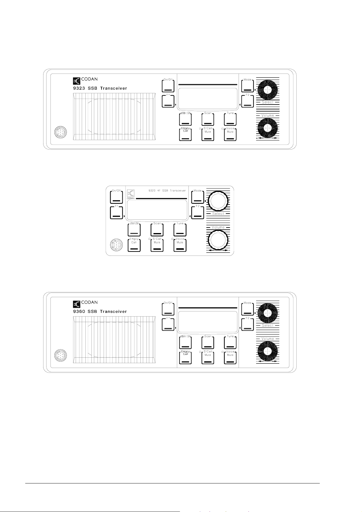
Figure 2 -1: Front panel of HF SSB Transceiver 9323
Figure 2 -2: Extended control head (9330) of HF SSB Transceiver 9323
Figure 2 -3: Front panel of HF SSB Transceiver 9360
2-2 HF SSB Transceiver 9323/9360/9390/9780 Technical Service Manual
Page 31
General information
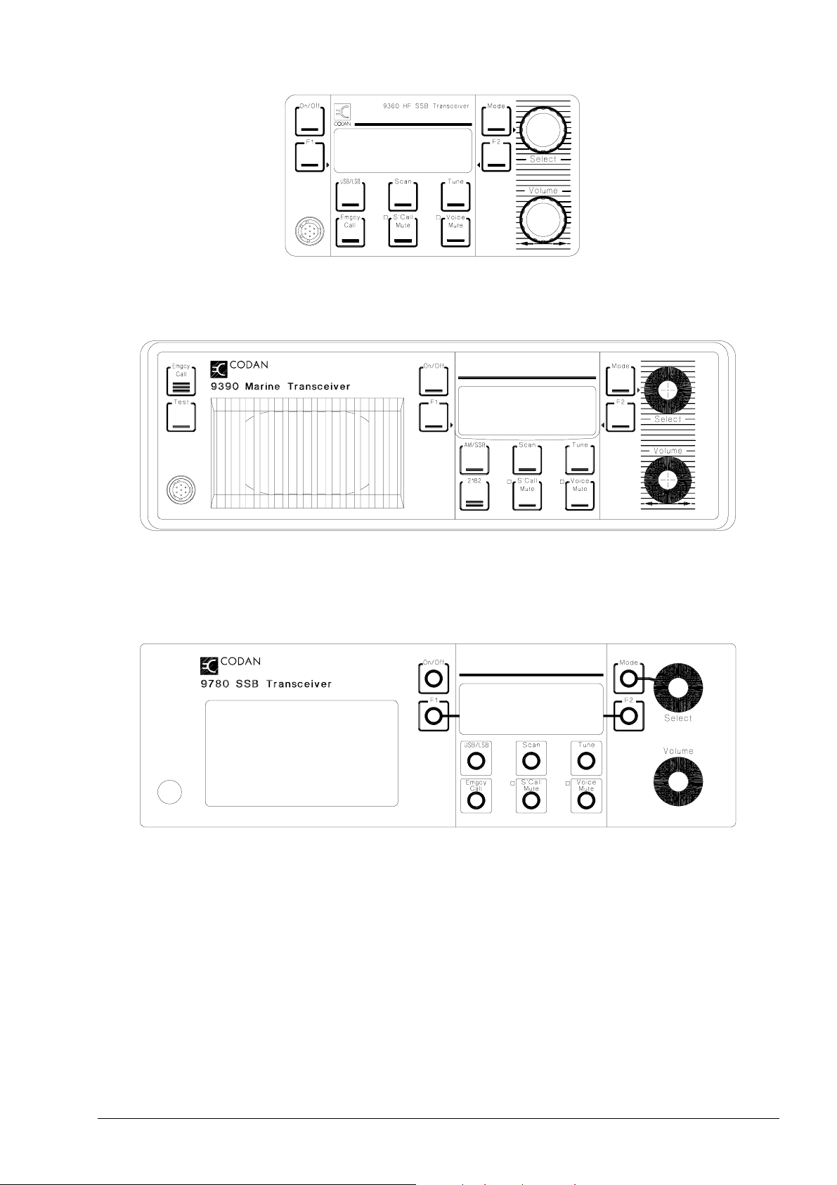
Figure 2 -4: Extended control head (9366) of HF SSB Transceiver 9360
Figure 2 -5: Front panel and extended control head (9391) of HF SSB Transceiver
9390
Figure 2 -6: Front panel of HF SSB Transceiver 9780
HF SSB Transceiver 9323/9360/9390/9780 Technical Service Manual 2-3
Page 32
General information
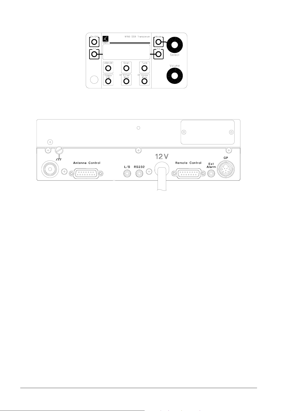
Figure 2 -7: Extended control head (9782) of HF SSB Transceiver 9780
Figure 2 -8: Rear panel of HF SSB Transceivers 9323, 9360, 9390 and 9780
For an explanation of the function of knobs, buttons and connectors on these
panels, see the relevant User Guide or Reference Manual. The User Guide for
each transceiver type details the elements of the Liquid Crystal Display (LCD).
2-4 HF SSB Transceiver 9323/9360/9390/9780 Technical Service Manual
Page 33

Specifications
Specification figures listed will normally be exceeded by production equipment.
Where relevant, acceptance limits are given in brackets. All measurements are
made at 13.6 V DC, with 50 Ω source and load resistances at 25°C ambient
temperature (unless otherwise specified).
General specifications
General information
Frequency range
Channel capacity
Frequency
generation
Operating modes
Frequency stability
9323 or 9390
Transmit: 2 to 26.5 MHz, (27 MHz CB band in Australia
only)
9360 or 9780
Transmit: 2.25 to 30 MHz, (optional 1.6 to 30 MHz)
Receive: 0.25 to 30 MHz
9323 or 9360
Up to 400 single or two-frequency simplex channels
9390
Up to 650 single or two-frequency simplex channels
9780
Up to 15 single or two-frequency simplex channels
All frequencies generated by synthesiser with 10 Hz resolution
Single sideband (J3E) USB or LSB or switched USB/LSB,
(AM: H3E optional)
USB: ±2 (3) ppm -30°C to +60°C
LSB: ±2 (3) ppm ±10 Hz
With high stability oven
USB: ±0.5 (1) ppm
LSB: ±0.5 (1) ppm ±10 Hz
Long term ageing
Oven warm up time
Programming
Cloning
Controls
HF SSB Transceiver 9323/9360/9390/9780 Technical Service Manual 2-5
1 ppm per year
1 minute
Frequencies and options are programmed via the microphone
socket or 3-wire RS232 interface using XP programming
software and an IBM compatible PC
Channels may be entered from the front panel by qualified
personnel or (where authorised) by the operator
Channel frequencies and options can be copied from one
transceiver to another via the microphone socket
Sealed membrane switches on the control panel and
microphone keypad
Rotary controls for volume and select functions
Page 34

General information
Indicators
Transmit/Receive
switching
RF input/output
impedance
Supply voltage
Overvoltage
protection
Supply current
Environment
Refer to illustrations for details
Using Option GP, 20 ms simplex operation, or 50 ms with up
to 1 MHz of separation between Tx/Rx frequency
50 Ω nominal
13.6 V DC nominal, negative earth
Normal operating range 10.5 to 15 V
Maximum operating range 9 to 16 V
Shut down at 16 V DC nominal for duration of overvoltage
Receive: no signal 750 mA
Transmit: see Transmit Specifications
Ambient Temperature Relative Humidity
-10°C to +30°C Head 95%
-30°C to +30°C TCVR From 95% at +30°C
+30°C to +60°C to 30% at +60°C
Note: -30°C Head to order
Cooling
Size and weight
Finish
Derate upper ambient temperature by 1°C per 330 m above
sea level
Convection or fan (Option F)
Transceiver only
250 mm W x 78 mm H x 350 mm D; 3.3 kg
With mounting cradle
270 mm W x 90 mm H x 350 mm D
Control head (9330/9366/9782)
130 mm W x 70 mm H x 40 mm D; 300 g
With mounting cradle
150 mm W x 80 mm H x 40 mm D
Control head (9391)
250 mm W x 78 mm H x 70 mm D; 750 g
With mounting cradle
250 mm W x 90 mm H x 70 mm D
Depth measurements include rear connectors/cables
Case: Silver-grey
Panel surround and heat sink: Matt black
Panel overlay: Lexan—Matt black (extended TCVR only)
Painted surfaces are scratch-resistant textured polyester
powdercoat
2-6 HF SSB Transceiver 9323/9360/9390/9780 Technical Service Manual
Page 35

Receiver specifications
General information
Type
Dual conversion,
superheterodyne
IF frequencies
45 MHz and 455 kHz
Sensitivity Frequency RF Amp OFF
0.25 to 2 MHz
2 to 26.25 MHz
Typical: 3 µV PD
0.35 (0.45) µV PD
-116 (-114) dBm
26.5 to 30 MHz
Typical: 0.5 µV PD
-113 dBm
Frequency RF Amp ON
2 to 26.25 MHz
0.12 (0.15) µV PD
-125 (-123) dBm
26.5 to 30 MHz
Typical: 0.18 µV PD
-122 dBm
For 10 dB SINAD with greater than 50 mW audio output
Input Protection
Selectivity
Will withstand 50 V RMS RF from a 50 Ω source
Greater than 70 (65) dB at -1 kHz and +4 kHz reference SCF
USB
Desensitisation
Blocking
Image rejection
Spurious responses
Cross modulation
Pass Band -6 (-8) dB
300 to 2600 Hz
Ripple 2 (4) dB PP
500 to 2500 Hz
10 dB SINAD reduced to 7 dB SINAD
-1 and +4 kHz (ref SCF) 65 (60) dB
±10 kHz 80 (75) dB
±50 kHz 95 (90) dB
As for Desensitisation
Better than 120 (110) dB
Better than 90 (70) dB
Self generated signals > 0.35 µV PD:
7303, 9125, 10950, 12775, 14607, 18250, 20075, 21900,
23725 kHz
A signal 90 (85) dB above a signal producing 10 dB SINAD,
modulated 30% and removed at least 20 kHz from the wanted
signal, will produce an increase in receiver noise of less than
3 dB
HF SSB Transceiver 9323/9360/9390/9780 Technical Service Manual 2-7
Page 36

General information
Intermodulation
AGC
AF response
AF power and
distortion
Clarifier
To produce a third order intermodulation product equivalent
to a wanted signal producing 10 dB SINAD, two unwanted
signals greater than 30 kHz removed from the wanted signal
must have a level greater than 82 (80) dB above the wanted
signal
Third order intercept (unaffected by AGC):
+8 (+5) dBm with RF amp off
-2 (-5) dBm with RF amp on
Less than 2 dB variation in output for input variation between
1.5 (2.5) µV and 100 mV PD
Fast attack, slow release
Typical: −1 dB 300 Hz to 1 kHz
Typical: −6 dB 1 kHz to 2.6 kHz
2.5 W into 8 Ω, 5% THD
4 W into 4 Ω, 5% THD
7 W into 2 Ω, 5% THD
Nominal: ±0.001%
Clarifier is automatically reset to mid-frequency with channel
change
Inband IMD
Signal to noise vs
input signal
Transmitter specifications
Power output 9323
Power output 9360
and 9780
Power output 9390
Duty cycle
Better than 25 dB IMD with two 100 mV PD RF inputs
An increase of input level of 40 dB above the sensitivity level,
increases the signal to noise at least 35 dB
100 W PEP at 2 MHz reducing with frequency to 85 W PEP at
26.5 MHz ±0.5 dB
27 MHz CB 10 W PEP
125 W PEP at 2.25 MHz reducing with frequency to 80 W PEP
at 30 MHz ±1 dB
CW or single tone: approximately 60% of PEP with average
PEP control
125 W PEP at 2 MHz reducing with frequency to 85 W PEP at
26.5 MHz ±1 dB
100% normal speech over full temperature range
100% ARQ up to 30°C
25% of 16 tone continuous data mode (5 minutes on
maximum) at ambient temperature up to 30°C
100% all modes up to maximum ambient of 45°C with
Option F
Supply current
Output power: 100/125 W
Two-tone or CW: 9 to 12 A
Average speech: 6 A for battery life calculations
2-8 HF SSB Transceiver 9323/9360/9390/9780 Technical Service Manual
Page 37

General information
Protection
AF response
Spurious and
harmonic emissions
Carrier suppression
Unwanted sideband
Intermodulation
(Two-tone test)
ALC
Safe under all load conditions by limiting reflected power to
10 W PEP and limiting PA transistor collector voltage swing
Thermal protection against excessive heatsink temperature
Overall response of microphone and transmitter rises
approximately 6 dB/octave 300 to 2700 Hz
Electrical input -6 (-8) dB, 300 to 2600 Hz
Ripple 2 (4) dB PP, 500 to 2500 Hz
Better than 55 (45) dB below PEP
60 (50) dB below PEP
70 (55) dB below PEP (400 Hz)
70 (65) dB below PEP (1 kHz)
100 W: 30 (26) dB below each tone, 36 (32) dB below PEP
125 W: 27 (26) dB below each tone, 33 (32) dB below PEP
A 10 dB increase in signal input above compression threshold
produces less than 0.5 dB increase in power output
Maximum ALC range greater than 30 dB
ALC attack time approximately 1 ms
Microphone
Dynamic type
HF SSB Transceiver 9323/9360/9390/9780 Technical Service Manual 2-9
Page 38

General information
Connectors
The following tables detail the pin connections and functions of the front and rear
connectors. Details are also provided for the cables used for channel and cloning
programming.
Microphone
Table 2 -1: Microphone connector (J3) pin function
Pin No. Function Signal Levels
1 Speaker Audio Output 12 V PP (max)
2 Microphone Input 50 mV PP
4 Ω (min)
12 kΩ I/P impedance
3 PTT Ground 0 V
4 Data In 0–5 V logic
5 PTT Active & Data Out Active low, 0–12 V logic
6 "A" Rail 13.6 V nominal
7 To Front Panel Speaker
Remote control
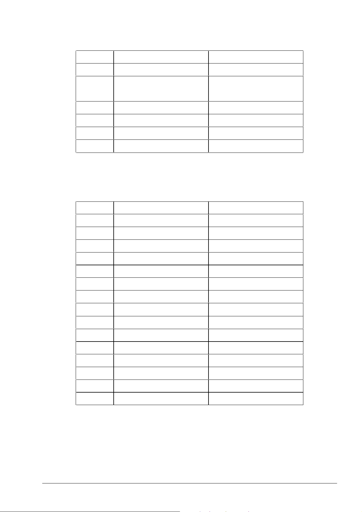
Table 2 -2: Remote Control connector (P204) pin function
Pin No. Function Signal Levels
1 Speaker 12 V PP
2 Remote PTT 5 V logic, Active low
3 EXT A/F I/P Future use
4 Power On
4 Ω min impedance
Momentary 0 V = PWR On
5 Data I2C5 V logic
6 No Connection
7Clock I
8 "S" & RF 4.5 to 0.25 V Rx
9 0 V Ground
2-10 HF SSB Transceiver 9323/9360/9390/9780 Technical Service Manual
2
C5 V logic
0 to 4.25 V Tx
Page 39
General information
Table 2-2 cont.
Pin No. Function Signal Levels
10 0 V Ground
11 Tx A/F 250 mV threshold
10 kΩ I/P impedance
12 Rx DEMOD O/P 1.5 V PP
13 Rx A/F O/P Post Mute 1.5 V PP switched
14 INT I2C5 V logic
15 "A" Rail
Antenna control
Table 2 -3: Antenna Control connector (J202) pin function
Pin No. Function Signal Levels
1 Channel Number bit 4 Active low (Open Collector)
2 Channel Number bit 8 Active low (Open Collector)
3EXT
4 Tune In/Out 5 V logic, Active low
5 Scan Antenna Active low (Open Collector)
6 No Connection
7 No Connection
8
+13.6 V nominal
PTT Out +10 V 1 kΩ source, Active high
9 Channel Number bit 1 Active low (Open Collector)
10 Channel Number bit 2 Active low (Open Collector)
11 Tuned In 5 V logic, Active low
12 "A" Rail +13.6 V nominal
13 "A" Rail +13.6 V nominal
14 Ground 0 V
15 Ground 0 V
HF SSB Transceiver 9323/9360/9390/9780 Technical Service Manual 2-11
Page 40
General information
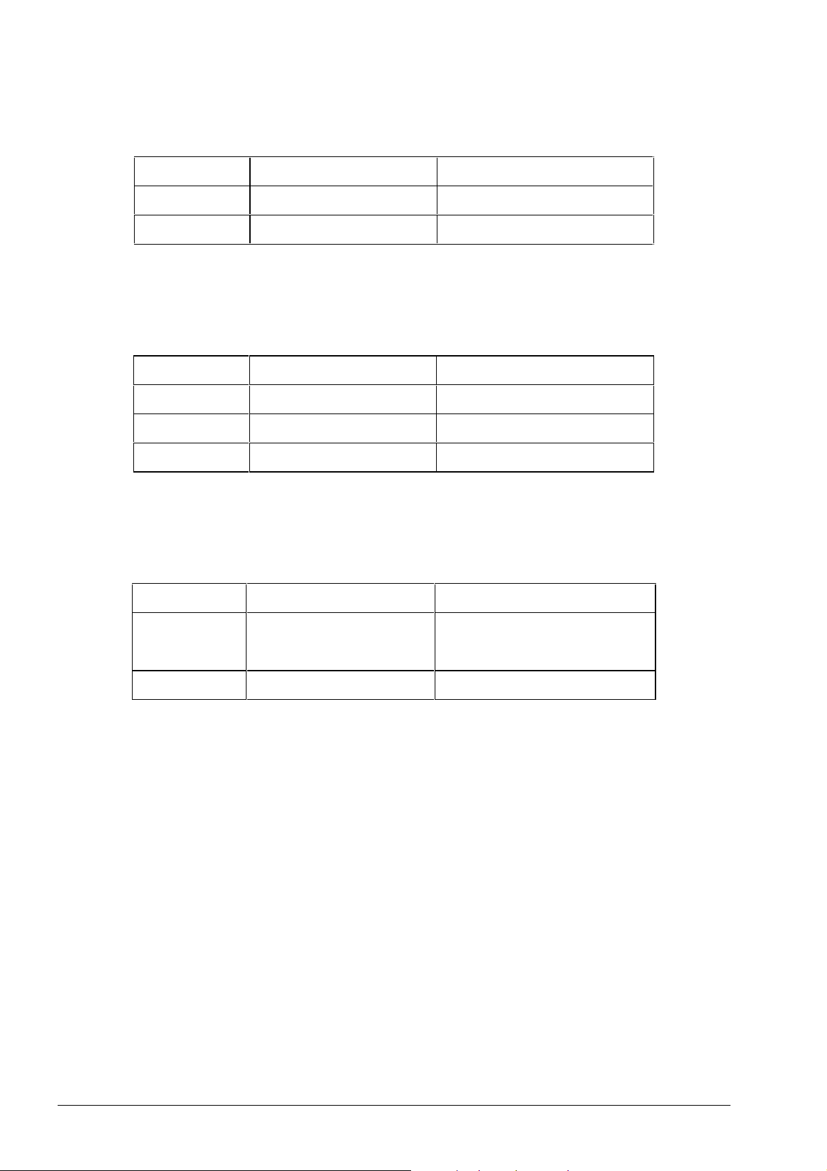
External alarm
Table 2 -4: External Alarm connector (J305) pin function
Connections Function Signal Levels
Tip External Alarm Contacts rated 50 V, 1 A
Sleeve Ground Closed to ground for alarm
RS232
Table 2 -5: RS232 connector (J101) pin function
Connections Function Signal Levels
Tip Data I/P RS232 I/P
Ring Data O/P 0–12 V O/P
Sleeve Ground Ground
Loudspeaker
Connections Function Signal Levels
Tip Speaker Audio Output 12 V PP max
Sleeve Ground 0 V
Table 2 -6: External loudspeaker connector (J206) pin function
4 Ω min impedance
2-12 HF SSB Transceiver 9323/9360/9390/9780 Technical Service Manual
Page 41
Option GP, general purpose
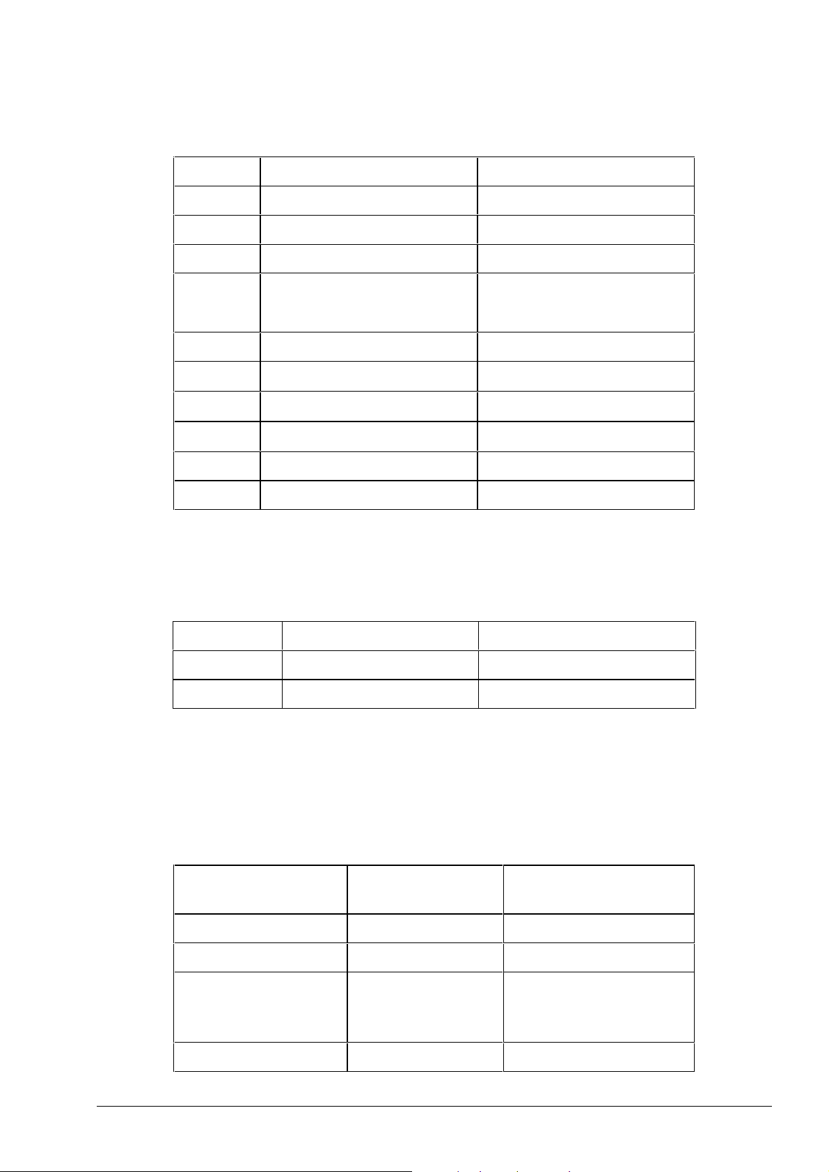
Table 2 -7: Option GP connector (J304) pin function
Pin No. Function Signal Levels
1 0 V Ground
2 Rx O/P 1.5 V PP
3 Tx I/P 170 mV PP Threshold
General information
4 Q Line
5 Alarm I/P 5 V logic I/P
6PTT
7SCAN
8"A" Rail
9 RS232 Rx RS232 I/P
10 RS232 Tx 0–12 V logic O/P
Option M, morse
Table 2 -8: Morse connector (J204) pin function
Connections Function Signal Levels
Tip Morse Input 5 V logic (Active low)
+10 V I/P = On
O/C = Off
Input 0 V = PTT
+10 V Output = Scan
+13.6 V nominal
Sleeve Ground 0 V
Programming cable
Codan part number 08-05137-001
Table 2 -9: Programming cable connector pin function
9-Way Computer
Serial Port Socket
2 5 Data from transceiver
3 4 Data to transceiver
5 series Thermistor
(Thermistor = 50 Ω
80°C)
7-Way transceiver
Microphone Socket
3 Ground
1/7 link Speaker Link
Pin Function
HF SSB Transceiver 9323/9360/9390/9780 Technical Service Manual 2-13
Page 42
General information
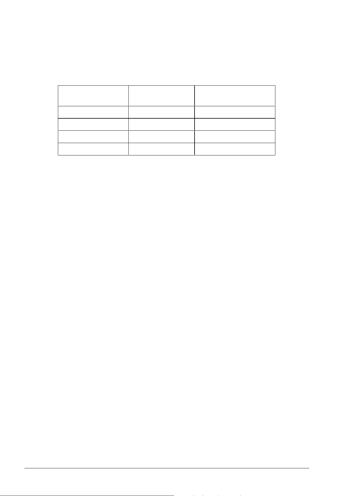
Cloning cable
Codan part number 08-05138-001
Table 2 -10: Cloning cable connector pin function
7-Way Transceiver
Microphone Socket
7-Way Transceiver
Microphone Socket
Pin Function
45Data I/O
54Data I/O
3 3 Ground
1/7 link 1/7 link Speaker Link
2-14 HF SSB Transceiver 9323/9360/9390/9780 Technical Service Manual
Page 43

Options
The following options are available for 9323, 9360 and 9390:
Code Options
ALE Automatic Link Establishment
AM Enable AM capability
1
ES*
Emergency Selcall
F Fit for continuous data transmission
GP General Purpose interface
GPS Global Positioning System capability
LF Fit for 1.6 to 2.25 MHz transmit frequency range
MMorse
PH Headphone output
2
S*
SL*
1
Selcall
Selcall Lockout
General information
*1 Included as standard in the 9360
*2 Included as standard in the 9323 or 9360, optional in 9390 only
The following options are available for 9780:
Code Options
AM Enable AM capability
LF Fit for 1.6 to 2.25 MHz transmit frequency range
MMorse
PH Headphone output
S Selcall with Selcall Lockout
ST Selcall and Telcall capability with Selcall Lockout
D Remote Diagnostics capability
TxD Programming of transmit frequencies from the front panel is
disabled
HF SSB Transceiver 9323/9360/9390/9780 Technical Service Manual 2-15
Page 44

Page 45

3 Brief description
This section of the manual provides a brief description of the major components
and circuit functions of the 9323, 9360, 9390 or 9780 transceiver as follows:
• control and switching functions
• synthesiser operation
• receive path
• transmit path
For an in-depth review of these functions see chapter 4 , Technical description.
HF SSB Transceiver 9323/9360/9390/9780 Technical Service Manual 3-1
Page 46
Brief description
PA and Filters
General
Read this description of the 9323, 9360, 9390 or 9780 transceiver in conjunction
with the Block Diagram 03-00902.
The 9323, 9360, 9390 or 9780 transceiver uses the same double conversion in
Receive and Transmit modes. Only the 45 MHz band-pass filter, the 455 kHz
sideband filter and the local oscillators VCO1 and VCO2 are common to both
modes of operation. The signal routing is determined by switching and control
voltages according to the mode selected.
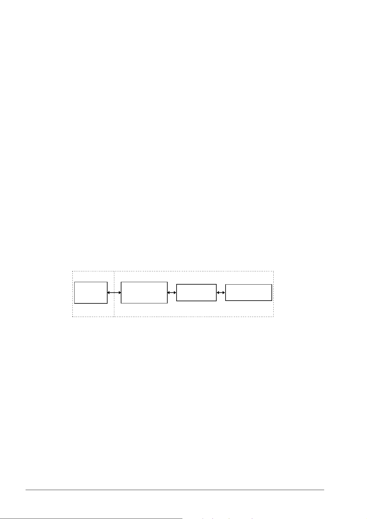
The circuits and functions of the 9323, 9360, 9390 or 9780 are located on four
major PCBs as shown in Figure 3-1:
• Display panel PCB
• Microprocessor and audio PCB
Micro and I/O
Transmit audio
Receive audio and Selective call
• Rx/Exciter PCB
RF Mixer and synthesiser
455 kHz IF modulator and demodulator
• PA and Filter PCB
Display
Panel
Microprocessor
and Audio
Rx/Exciter
Figure 3 -1: 9323, 9360, 9390 and 9780 PCB block diagram
3-2 HF SSB Transceiver 9323/9360/9390/9780 Technical Service Manual
Page 47

Control and switching
Most of the transceiver functions are microprocessor controlled. The channel
frequencies are programmed via the microprocessor to the Electrically Erasable
Programmable Read Only Memory (EEPROM). The remaining facilities are preprogrammed in the Erasable Programmable Read Only Memory (EPROM).
The power On function is controlled by hardware and the power Off function is
controlled by software. The rotary volume control is a digital contacting encoder.
It controls a 16-step attenuator in the audio signal path between the preamplifier
(after the demodulator) and the amplifier. This drives the loudspeaker.
Brief description
HF SSB Transceiver 9323/9360/9390/9780 Technical Service Manual 3-3
Page 48

Brief description
Synthesiser
The 9323, 9360, 9390 or 9780 transceivers use single loop synthesisers. The main
synthesiser (VCO1) generates an oscillator frequency in 2 kHz steps. In receive,
the oscillator frequency ranges from 45.250 MHz to 75 MHz. In transmit the
oscillator frequency will depend on the transceiver type and the options fitted. It
will be within the range of 46.6 MHz to 75 MHz.
The vernier synthesiser (VCO2) generates oscillator frequencies of 44.5435 MHz
to 44.5455 MHz in 10 Hz steps.
The synthesisers are controlled by the same process that controls the remainder of
the transceiver. Serial data representing the various pre-programmed channel
frequencies is loaded into both synthesisers.
When upper sideband is selected, the 9323, 9360, 9390 or 9780 uses a single
crystal reference oscillator of 7304 kHz. The reference oscillator is also used to
provide the 456.5 kHz (7304 kHz divided by 16) signal for the audio
modulator/demodulator.
For lower sideband operation a separate crystal oscillator is selected, operating at
1814 kHz to provide 453.5 kHz (1814 kHz divided by 4) to the audio
modulator/demodulator.
3-4 HF SSB Transceiver 9323/9360/9390/9780 Technical Service Manual
Page 49

Receive path
PA and Filter PCB
The received signal from the antenna passes through a PA low-pass filter, onto the
transmit/receive relay. It is then sent to the receiver input on the Rx/Exciter PCB.
Rx/Exciter PCB
From the receive input, the signal passes through a selected high-pass filter and is
fed either directly to a 30 MHz low-pass filter or via an RF amplifier. The output
of the low-pass filter is fed to the input of the first balanced mixer. Here it mixes
with the local oscillator VCO1 to produce an IF signal centred on 45 MHz.
The 45 MHz signal is filtered using a 15 kHz wide band-pass filter before being
applied to the second balanced mixer. The signal mixes with a second local
oscillator VCO2 producing an IF signal centred on 455 kHz.
The output of the second mixer divides into two paths:
Brief description
• the main path passes the signal through a noise gate to a 2.5 kHz sideband filter
where only the wanted sideband passes to the high gain AGC controlled IF
amplifier
• the second path passes the signal through an amplifier that detects noise and
controls the noise gate to remove impulse noise, such as car ignition, from the
455 kHz signal
The amplified 455 kHz signal is demodulated to produce an audio signal. It is then
amplified. The amplified audio signal operates an AGC circuit. This controls the
IF amplifier gain to prevent overloading when receiving strong signals. It is also
used to maintain a constant audio output with changing input signals.
The amplified audio signal is fed via a mute gate to the volume control. The mute,
when enabled, removes the receiver noise from the speaker. When speech is
detected, the gate in the audio line closes to allow the signal to be heard.
The signal from the volume control is applied to a power amplifier IC to drive the
transceiver’s loudspeaker.
HF SSB Transceiver 9323/9360/9390/9780 Technical Service Manual 3-5
Page 50

Brief description
Transmit path
Microprocessor and Audio PCB
The microphone audio is amplified and levelled in the microphone
amplifier/compressor, then fed to a balanced modulator.
Rx/Exciter PCB
When mixed with the local oscillator, the double sideband output of the modulator
is applied to a 2.5 kHz sideband filter centred on 455 kHz, passing only the
wanted sideband to the first mixer. Here it mixes with the local oscillator VCO2 to
produce an IF signal centred on 45 MHz.
The transmit signal is filtered by the 15 kHz wide band-pass filter before being fed
to the input of the second mixer.
At the second mixer, the signal mixes with the output of oscillator VCO1 to
produce the required channel frequency. It passes through a 30 MHz low-pass
filter to the PA and Filter PCB.
PA and Filter PCB
On the PA assembly, the signal is amplified, then it is passed through the
transmit/receive relay to the selected band filter. The output from the filter is fed
via the VSWR detector to the antenna output connector. From here it is connected
by coaxial cable to the antenna.
The VSWR detector monitors the forward and reflected power and controls the
power output of the transmitter. If a high VSWR is detected, the power output is
reduced to protect the PA.
3-6 HF SSB Transceiver 9323/9360/9390/9780 Technical Service Manual
Page 51

4 Technical description
This section of the manual contains a technical description of the 9323, 9360,
9390 or 9780 transceiver and 9330, 9366, 9391 or 9782 control head. It should be
read together with the drawings in chapter 9, Drawings.
Control and supply voltages
All switching, except power On, is controlled either directly or indirectly by the
microprocessor IC101 (located on the Microprocessor and Audio PCB) in
conjunction with the microprocessor IC2 in the control head.
Power on
1 04-02974
When the On/Off button on the control panel is pressed, the PWR ON line (P4
pin 3) is pulled low via the series circuit consisting of diode D1 on the On/Off
button and D3.
The cathode of D3 is at 0 V prior to switch on, permitting the PWR ON line to
momentarily be held low by discharged capacitors on the 5 V rail.
1 04-02976 Sheet 2
The PWR ON line on the front panel is connected via a short cable to P201 pin 3
located on the Microprocessor and Audio PCB. From there it is fed via R222 to
the base of transistor V203.
1 04-02976 Sheet 2
The PWR ON line from the extended control head is connected by a control cable
to the transceiver rear panel connector P204 pin 4, then via a ribbon cable to the
Microprocessor and Audio PCB (P203 pin 7). From there it is fed through an RF
suppression network (L205 and C236) then connected in parallel to the front
PWR ON line, then via R222 to the base of V203.
With the PWR ON line low, V203 conducts and energises the ON coil of latching
relay K201 resulting in contacts K201 closing and applying a ground to the TCVR
ON line.
The TCVR ON line is connected from the Microprocessor and Audio PCB via
P101 pin 3 (see Sheet 1) to P1 pin 3 on the PA assembly [1 04-02973 and
04-03096] and finally to the negative side of relay K8.
If the polarity of the DC supply is correct and below 16 V, V4 will conduct and
relay K8 will energise, closing contacts K8-1 and connecting the DC supply to the
transceiver. The PWR ON line is disabled on start up when D3 on the control head
is reverse biased by the 5 V supply.
HF SSB Transceiver 9323/9360/9390/9780 Technical Service Manual 4-1
Page 52

Technical description
Power off
If the DC supply voltage exceeds 16 V, zener diode V2 conducts causing V3 to
also conduct and switch off V4, thus preventing K8 from energising.
Diode D7 prevents relay K8 from operating if the DC supply is reverse polarised.
The power input circuit is protected from high voltage transients by Voltage
Dependent Resistor (VDR) R8.
If the On/Off button on the control panel is pressed [1 04-02974] when the
transceiver is operational, a scanning active low pulse from the microprocessor
IC2 pin 11 is applied to the input port of IC1. The interrupt line (pin 13)
momentarily goes low, indicating to the microprocessor IC2 to read the input ports
of IC1 and to switch off the transceiver.
The switch off command is sent from IC2 (pins 22 and 23) via the external I2C
bus to microprocessor IC101 on the Microprocessor and Audio PCB [1
04-02976 Sheet 1] pins 22 and 23.
Microprocessor IC101 outputs data on the local I2C bus to IC109 pins 23 and 24,
latching pin 5 on the PWR OFF line low. The OFF coil of latching relay K201
(see Sheet 2) energises, opening K201 contacts and releasing the power relay K8
on the PA assembly, thus switching off the transceiver.
Supply voltages
The supply voltages on the Display Panel PCB [1 04-02974] are shown in
Table 4-11.
Table 4 -11: Display Panel PCB supply voltages
Supply Description Regulator
"A" rail unregulated battery supply
"B" rail 10 V regulated supply IC9
+5 V 5 V regulated supply IC11
-7 V -7 V from charge pump supply IC7
4-2 HF SSB Transceiver 9323/9360/9390/9780 Technical Service Manual
Page 53
Technical description
The supply voltages on the Microprocessor and Audio PCB [1 04-02976] are
shown in Table 4-12.
Table 4 -12: Microprocessor and Audio PCB supply voltages
Supply Description Regulator
"A" rail unregulated battery supply
"B" rail 10 V regulated supply IC201
+5 VA 5 V regulated supply IC202
+5 VB 5 V regulated supply IC203
The supply voltages used on the Rx/Exciter PCB [1 04-02972] are shown in
Table 4-13.
Table 4 -13: Rx/Exciter PCB supply voltages
Supply Description Regulator
"A" rail unregulated battery supply (supplies
the crystal oven only)
"B" rail +10 V regulated supply IC201
+5 VB 5 V regulated supply IC203
+18/26 V 18 & 26 V from the charge pump
*
*
IC11
supply
*
Regulator is located on the Microprocessor and Audio PCB [1 04-02976]
The supply voltages on the PA and Filter PCB [1 04-02973 and 04-03096] are
shown in Table 4-14.
Table 4 -14: PA and Filter PCB supply voltages
Supply Description Regulator
"A" rail unregulated battery supply
+5 V 5 V regulated supply selected in
IC2
transmit only
+5 V 5 V supply (supplies IC1 only) V1
HF SSB Transceiver 9323/9360/9390/9780 Technical Service Manual 4-3
Page 54

Technical description
Receive/Transmit switching
The main transmit/receive DC switching circuit originates from the latched output
of IC209 pin 6 located on the Rx/Exciter PCB [1 04-02972 and 04-03135
Sheet 2]. IC209 pin 6 is connected to two transistors V209 and V212. V209
governs the AGC function. V212 forms part of the circuit controlling the transmit
and receive mixer circuits.
When the Receive mode is selected, the output of IC209 pin 6 is latched to 0 V,
switching V209 off and allowing the AGC to function normally. V212 is also
switched off, allowing the first NAND gate of IC6/D to be pulled high by resistor
R42. This sets the output of IC6/D pin 11 low, switching on V2 and V6, thus
enabling the receive mixers IC4 and IC7. The output of the second NAND gate
IC6/C will go high, switching V3 and V7 off and inhibiting the transmit mixers
IC5 and IC8.
When the PTT inputs are detected by the microprocessor IC101 [1 04-02976
Sheet 1] it sends a command via the local I2C bus to IC209 [1 04-02972 and
04-03135 Sheet 2] to latch the output pin 6 high (+5 V). This causes V209 in the
AGC circuit to conduct, setting the AGC to 0 V and disabling the 455 kHz IF
amplifier. Resistor R255 provides a small DC offset to IC205/A to ensure the
AGC always switches to 0 V.
With IC209 pin 6 latched high, V212 conducts, setting the input of IC6/D pin 13
low. This in turn sets the output of IC6/D pin 11 high, thus switching off V2 and
V6, disabling the receive mixers IC4 and IC7 and providing the DC voltage to
enable the transmit mixers IC5 and IC8.
The noise limiter in Transmit mode is disabled by V7 conducting, thus applying a
DC level via D201 and R203 (see Sheet 2) to the AGC input pin of noise
amplifier IC201 pin 5.
DC from V7 has two other functions. It provides bias via R238 to IC202 pin 5 to
enable the modulator. It also biases V5 (see Sheet 1) on, clamping the base of V4
to 0 V, thus preventing D19 from conducting and attenuating the transmit signal.
Serial data from the microprocessor IC101 [1 04-02976 Sheet 1] is also applied
to IC1 on the PA assembly. When transmit is selected, a ground on pin 12
energises the transmit/receive relay K7. The path is now completed from the PA
output to the antenna.
In Transmit mode, the microprocessor IC101 outputs a low from pin 28. This is
applied to the input of inverter buffer IC207 pin 12 (see Sheet 2). The high at the
output pin 14 is connected to:
• the antenna control connector P202 pin 15
• the optional PCB output P204 pin 12
• the mute squaring amplifier IC307/B via R365 and D307 (see Sheet 3)
The DC applied to IC307/B applies a small offset to disable the squaring amplifier
during transmission.
4-4 HF SSB Transceiver 9323/9360/9390/9780 Technical Service Manual
Page 55

Receiver
Input low-pass filter s
1 04-02973 and 04-03096
The receiver input signal is fed through one of six relay-selected, PA Low-Pass
Filters (LPF) K1–K6. The signal is then fed via the transmit/receive relay K7 and
signal clamping diodes D3–D6 to connector J3.
High-pass filters
1 04-02972 and 04-03135 Sheet 1
From J3 on the PA assembly, the High-Pass Filter (HPF) is connected by a coaxial
cable to J2 located on the Rx/Exciter PCB. Six HPFs are used to complete the
band-pass filter (BPF) characteristics. These are diode switched according to the
frequency band in use, by grounding the appropriate select line from IC1. For
broadcast channels below 2 MHz, a 14 dB resistive attenuator is selected instead
of a filter.
Technical description
RF amplifier
This is an example of how the HPF works. If the HPF 2-3.1 is selected, IC1 pin 10
switches from 10 V to 0 V. This completes the input DC switching current path
from the "B" rail via R2, L1, D11, L18 and R14 to 0 V. Diode D11 is forward
biased and passes the receive signal to the input of the selected HPF.
The output DC switching current path from the "B" rail consists of R3, L2, D12,
L20 and R15 to 0 V. With D12 forward biased, the receive signal at the output of
the 2-3.1 HPF can either be fed directly via D15 and C57 to the following 29 MHz
low-pass filter (LPF) or via D16 to the input of the RF amplifier.
1 04-02972 and 04-03135 Sheet 1
The RF amplifier (consisting of V1 and its associated components) has a nominal
gain of 12 dB. It can be selected from the front panel on the control head. When
the RF amplifier is selected, IC2 pin 12 goes high, switching the output of IC3/A
and B (in parallel) from 0 V to approximately 10 V. This action applies DC volts
via RF filter inductor L27 to the primary of T2, then to the series inductors of the
LPF L26-L24 to the collector of V1. The DC volts also forward biases V1 via
feedback resistor R24.
With the RF amplifier selected, the voltage on the base of V1 is positive with
respect to the output of the HPF network, thus forward biasing D16. This allows
the signal to pass to the input of the RF amplifier. At the same time, D15 is
switched off, as the cathode is held approximately 2 V positive with respect to the
anode.
HF SSB Transceiver 9323/9360/9390/9780 Technical Service Manual 4-5
Page 56

Technical description
LPF and first mixer
1 04-02972 and 04-03135 Sheet 1
The output from the HPF is fed direct, or via the RF amplifier, to a 29 MHz LPF
(C59, L24, C60/61, L25, C62, & L26) and then via transformer T2 to the balanced
input of the first mixer IC4 pins 12 and 13.
Mixer IC4 is a combined amplifier/balanced mixer with a gain of approximately
20 dB. The received signal is mixed with the output of the Voltage Controlled
Oscillator (VCO1), then applied to pin 5. This operates between 45.250 MHz and
75 MHz to produce a balanced IF output (pins 3 and 14) centred at 45 MHz.
DC is applied to the mixer IC4 pins 3 and 14 via the filtered "B" rail and the
centre tap of the mixer output transformer T3. In Receive mode, V2 is conducting
and supplies the filtered "B" rail to IC4 pin 4 and 11, via R34 and R36
respectively.
45 MHz band-pass filter
Second mixer
Noise limiter
1 04-02972 and 04-03135 Sheet 1
The 45 MHz IF signal is filtered through a 15 kHz BPF (centred on 45 MHz)
consisting of T3, Z1, L30, Z2 and T4. This removes unwanted signals produced by
the first mixer. The filtered output is applied via coupling capacitors C84 and C85
to the balanced input of the second mixer IC7 pins 12 and 13.
1 04-02972 and 04-03135 Sheet 1
Mixer IC7 is a combined amplifier/balanced mixer and identical to mixer IC4.
The 45 MHz signal is mixed with the output of the second Voltage Controlled
Oscillator (VCO2), then applied to pin 5. This operates between 44.5435 MHz
and 44.5455 MHz to produce a second IF centred at 455 kHz.
DC to the mixer output is provided by the filtered "B" rail, which is connected to
the centre tap of the 455 kHz output transformer T201 (Sheet 2). It is then fed to
the mixer output transformer T3. In Receive mode when V6 is conducting, the "B"
rail provides DC via R45 to IC7 pin 4 and bias via R47 to pin 11.
1 04-02972 and 04-03135
The 455 kHz output of IC7 pins 3 and 14 is applied via C201, R201, C202 and
R202 to the balanced input of a high gain amplifier IC201 pins 4 and 6.
The balanced outputs at pins 1 and 8 are connected to a tuned auto transformer
T202 (455 kHz). The output of T202 is applied to the base of V201, which is an
active rectifier. Noise bursts produce positive going pulses at the collector of
V201 and trigger, via V202, the monostable flip-flop IC6A/B. The pulse width is
determined by C208 and R210 (nominally 250 µs).
4-6 HF SSB Transceiver 9323/9360/9390/9780 Technical Service Manual
Page 57

The outputs of the flip-flop pins 3 and 4 produce complimentary pulses that are
connected to the FET gates of V204 and V205. These gate out the noise bursts
from the 455 kHz signal. With V204 on and V205 off, the IF signal is passed to
the sideband filter Z202. When a noise burst is present, V204 is switched off and
V205 is switched on, blocking the IF signal for the period of the gate pulse.
The average DC component of V201’s collector current is used as an automatic
gain control to IC201. It is applied via R206 to pin 5. This ensures that only the
noise burst signal triggers the monostable. The AGC decay constant is set by the
components C204 and R205.
In transmit, IC201 is disabled (see page 4-4, Receive/Transmit switching).
455 kHz filter and IF amplifier
1 04-02972 and 04-03135 Sheet 2
The IF signal from the noise blanker gate V204 is applied to a 2.5 kHz ceramic
filter Z202. The filter removes the unwanted sideband, adjacent channels and
other unwanted products generated by the second mixer. The wanted sideband,
centred at 455 kHz, is passed by the filter to a two-stage gain controlled amplifier,
consisting of V207, V208, and its associated components.
Technical description
The IF amplifier is broadly tuned to 455 kHz by the tuned circuits L202/C219 and
L203/C223.
Demodulator
1 04-02972 and 04-03135 Sheet 2
The output of the 455 kHz IF amplifier is passed via coupling capacitor C224 to
the input of a double balanced mixer IC203 pin 1. The IF signal is mixed with the
local oscillator that is applied to pins 8 and 10 to produce an audio output at IC203
pin 6. The local oscillator operates at 456.5 kHz for USB conversion and
453.5 kHz for LSB. For details of operation of the local oscillator see page 4-18,
455 kHz local oscillator for USB/LSB.
©
Local oscillators VCO1 and VCO2 shift by a total of 3 kHz when switching from
USB to LSB. This enables filter Z202 to be used for either sideband.
Automatic gain control
1 04-02972 Sheets 1 and 2
An Automatic Gain Control (AGC) is applied to a number of stages in the
receiver. This is used to increase the dynamic range of the receiver and to maintain
an almost constant audio output level for a large variation of input signals.
When the receiver is at maximum gain, the AGC at the output of IC205/A pin 1
(TP205) (see Sheet 2) is nominally 5.5 V. This is set by the resistor divider R257
and R258 in conjunction with the gain setting resistors R254 and R259.
HF SSB Transceiver 9323/9360/9390/9780 Technical Service Manual 4-7
Page 58

Technical description
The demodulated audio output from IC203 is first amplified by IC204/A then
passed via a resistive attenuator (R263 and R264) to a full wave active peak
rectifier circuit V210 and V211.
Under no signal conditions, IC204/A output, V210 and V211 bases and emitters
are all at the same potential of 5 V. When the audio swing at the output of IC204
exceeds approximately ±0.75 V (from 5 V), it causes V210 to conduct during the
positive peaks and V211 during the negative peaks. The common collector output
charges capacitor C237 during the transistor’s conducting period. The resulting
DC is applied to inverting amplifier IC205/A causing the AGC output to drop to a
level determined by the strength of the received signal. This lowers the voltage
applied to gate 2 of both FETs V207 and V208, reducing the overall gain of the
455 kHz IF amplifier.
AGC is applied to a second inverting amplifier IC204/B to extend the dynamic
range of the receiver. Its output produces an inverted AGC, nominally 0 V under a
no signal condition, but starts to rise once the input to IC204/B falls below 3.2 V
(set by R249 and R250).
The inverted AGC from IC204/B is divided into two paths:
• one path is connected via R223 to gate 1 of V207, improving the gain control
of the 455 kHz IF amplifier
• the second path is via a delay and damping network (R221/V206, R220, C215,
D203, and R41) to the base of V4 (see Sheet 1)
The pin diodes D19 across the first mixer output act as variable resistors. The
resistance falls as V4 collector current increases with a rise in AGC, thus reducing
the mixer output gain at high signal levels.
Another AGC circuit is incorporated at the output of the second mixer. It is used
for signals that are out of the 2.5 kHz sideband frequency, but within the 15 kHz
BPF bandwidth (see Sheet 1). V15 is connected between one side of the balanced
output and the "B" rail. When the output swing from the mixer IC7 exceeds 0.7 V
between the base and the rail, V15 conducts and reduces the gain of the first mixer
by increasing the current through the pin diodes D19.
The AGC fast attack time is set by R262, R263 and R264 in the emitter circuit of
the peak rectifiers V210 and V211 (see Sheet 2). Capacitor C237 charges and the
resultant slow decay time of C237 is through the resistor network R260 and R259.
The attack and decay time will vary at different signal strengths, but nominally are
about 2 ms and 0.5 s respectively. Resistor/diode networks R276/D207 and
R277/D208 are connected to outputs on IC209 (pins 4 and 5) and can be
grounded, under software control. This reduces the AGC decay time constant
when required for special applications.
4-8 HF SSB Transceiver 9323/9360/9390/9780 Technical Service Manual
Page 59

Voice mute
Technical description
1 04-02976 Sheets 1, 2 and 3
The audio at the output of IC204/A on the Rx/Exciter PCB [1 04-02972
Sheet 2] is connected via P201 pin 9 (Rx Audio) to the Microprocessor and Audio
PCB pin 9 (see Sheet 2). It is then coupled via C206 to the input of IC307A (see
Sheet 3), which operates as a squaring amplifier. At the open collector output, the
squared signal across load resistor R352 charges C343 via D308 during the
negative excursions. The charge is transferred to C344 by V303 during the
positive excursions. The resultant DC voltage on C344 is proportional to the
frequency of the audio (i.e. voltage rises as frequency increases). The squaring
amplifier is disabled in transmit by applying a DC offset from IC207 pin 14
(Sheet 2) via D307 and R365 to IC307/B pin 5.
IC304/B and its associated components function as an LPF with a cut-off
frequency of approximately 10 Hz. The output from IC304/B is a DC voltage
varying at the syllabic rate of the received speech.
IC307/C and IC307/D form a window comparator. The window width is adjusted
by the mute sensitivity preset R357. The divider network R359 and R360 together
with C348 averages the output of IC304/B to provide the reference voltage for the
window comparator. If the output from IC304/B rises or falls below this reference
by the amount set by R357, then the open collector outputs of IC307/C and
IC307/D will discharge C349, applying a low to the input of comparator IC307/B
pin 6.
The second input of comparator IC307/B pin 7 is set to 4 V by resistor divider
R363 and R364. When input pin 6 falls below 4 V, the comparator output at pin 1
goes high (MUTE DET line). This indicates to the microprocessor IC101, via
IC111 pin 5 (see Sheet 1), that speech has been detected.
Mute detection timing is controlled by discharging C349 through R361 for a fast
attack and charging C349 via R362 for a slow release (about 3 seconds).
When Voice Mute mode is selected by the Voice Mute button on the control
panel [1 04-02974], the microprocessor IC2 on the control head sends a signal
via the external I2C bus to the microprocessor IC101 on the Microprocessor and
Audio PCB [1 04-02976 Sheet 1]. The microprocessor IC101/A sends a
command via the local I2C bus to IC114 to latch the mute switch pin 19 low. This
applies a low to IC206/D pin 12 (see Sheet 3), which opens the mute gate and only
allows a very low level of audio to pass via R330 (when fitted) to the volume
control circuit.
When voice is detected by the mute circuit, a high is applied to IC111 pin 5
(MUTE DET line). The interrupt pin (pin 13) momentarily goes low, informing
the microprocessor to read the input ports of IC111. This will indicate to the
microprocessor that the mute detect line is high. The microprocessor then sets the
mute switch IC114 pin 19 high and closes the mute gate IC206/D (see Sheet 3).
The audio is then passed to the volume control circuit.
HF SSB Transceiver 9323/9360/9390/9780 Technical Service Manual 4-9
Page 60

Technical description
Volume control and audio output amplifier
1 04-02974, 04-02976 Sheets 1 and 3
The volume control circuit is a 16-step attenuator and consists of R334–R340.
Each step has ≈4 dB of attenuation, giving a total of 64 dB.
The rotary volume control is a digital contacting encoder. When this control is
rotated in either direction, the microprocessor IC2 on the Display Panel PCB [1
04-02974] reads each position change. It sends commands via the external I2C bus
to the microprocessor IC101 on the Microprocessor and Audio PCB (see Sheet 1)
to select the appropriate audio attenuators. The microprocessor IC101 then sends
data via the local I2C bus to change the output ports of IC114 pins 3–6. This action
controls the analogue switches that switch the step attenuator in and out.
The audio is passed from the buffer amplifier IC304/A, through a resistor
attenuator R342 and R343, to the input of the loudspeaker amplifier IC306.
The maximum output of the audio amplifier is either:
• 2.5 W into an 8 Ω speaker
• 8 W into a 2 Ω speaker
Warning beeps are heard if the maximum or minimum limits of the volume
control are reached. The warning beeps are generated from the tone generator
IC106 pin 10 [1 04-02976 Sheet 1]. The tone is fed via a resistor attenuator
network to the input of the loudspeaker amplifier IC306 (BEEPS I/P line). The
beep audio level is varied by the volume control. The level is controlled by the
microprocessor, which selects the appropriate attenuator shunt resistors (R138,
R140 and R142) to ground (IC109 pins 8, 9 and 10).
Low voltage Tx inhi bit
1 04-02972 and 04-03135 Sheet 2
The comparator IC211A on the Rx/Exciter PCB monitors the "A" rail. When the
supply voltage drops to 9 V, the output of IC211A is pulled low thus disabling the
PTT line connected from IC209 pin 6 via R275 to transistor switch V212. This
function prevents the transceiver latching in Tune mode when the supply voltage
drops below 9 V.
4-10 HF SSB Transceiver 9323/9360/9390/9780 Technical Service Manual
Page 61

Transmitter exciter
Microphone amplifie r /compressor
1 04-02974 and 04-02976
The microphone insert is a moving coil device and is active when the PTT button
is pressed. This removes the short circuit across the microphone, and at the same
time, applying a ground to the PTT line on J1 pin 5.
The microphone is connected to the control panel via J3 pins 2 and 3 [1
04-02974] and to the PCB via P3 pins 1 (ground) and 5. From there, the
microphone audio is passed through an RF filter network R24 and C21 to the
input of the preamplifier IC10/B.
When the microphone is not in use, the input switch (consisting of transistor V10
and associated components) disables the audio by applying a short across the
input.
Technical description
The audio output of amplifier IC10/B is fed through an RF decoupling network
(R40, C41 and R44) to connector P4 pin 2. In the front panel control version, the
audio is connected to P201 pin 2 on the Microprocessor and Audio PCB [1
04-02976 Sheet 2). From there it is fed via capacitor C219 and analogue switch
IC206/A to the combining amplifier IC204/A.
For the control head version, the Tx audio at connector P4 pin 2 is fed via a
control cable to P204 pin 11 on the transceiver. From there the output is connected
via a ribbon cable to P203 pin 6 on the Microprocessor and Audio PCB [1
04-02976 Sheet 2]. The audio path continues from pin 6 via a second RF
suppression network (R229/B and C242), through C218 and analogue switch
IC206/C to the combining amplifier IC204/A.
Additional audio inputs are applied to the combining amplifier IC204/A from:
• the tone generator IC106 via R213
• the optional PCB (P204 pin 3) via R214
• the option PS input (P303 pin 5) via C217, analogue switch IC206/B and R216
The microphone audio at the output of IC204/A is applied to the input of a
microphone compressor amplifier consisting of IC204/B, IC205/A and B, V202
and associated components. This provides a constant output for a large variation
in speech levels applied to the input (≈30 dB range).
When there is no speech present, the amplifier IC204/B is set to the maximum
gain. This is determined by the feedback resistor R208 and the shunt FET V202,
which functions as a variable resistor (minimum resistance is ≈150 Ω for
maximum gain).
The output of amplifier IC204/B is connected to the inputs of IC205/A and
IC205/B forming a window comparator. The window is set by the divider chain
R204–R207 to be centred at 5 ±0.25 V.
HF SSB Transceiver 9323/9360/9390/9780 Technical Service Manual 4-11
Page 62

Technical description
When the level of the speech input applied to the microphone amplifier is greater
than ≈3.5 mV P (compression threshold), the output swing will exceed the
comparator window (±0.25 V). This produces negative going output pulses from
the comparator IC205/A and B pins 1 and 7. These pulses lower the DC charge on
capacitor C212. The effect is that the voltage will be reduced on the FET gate of
V202. This increases the resistance of the FET and lowers the gain of the
microphone. This puts the microphone amplifier into compression. The output
level remains constant for a further 30 dB increase in input level before
overloading occurs.
Under normal speech conditions, the time constant (consisting of C212 and
R211), sets the talk power ratio and produces a high average transmission power
level. When data transmission is required, the time constant is extended by
switching in capacitor C213 in parallel to C212 (TALK PWR OFF line). This is
achieved by a command from the microprocessor IC101 [1 04-02976 Sheet 1] to
set the output port of IC114 pin 10 low, thus grounding the negative side of C213.
When lower power is required for CB channels, the drive level to the PA is
reduced by the microprocessor IC101 setting IC114 pin 9 low. This causes FET
V201 (see Sheet 2) to switch on and apply R203 in parallel to resistors R205 and
R206. This action reduces the comparator window to ±0.125 V, resulting in a
reduction of 6 dB in the audio output from the microphone compressor amplifier
IC204/B.
Modulator
1 04-02972 and 04-03135 Sheet 2
The transmitter audio output of IC204/B is passed via P102 pin 4 to the
RF/Exciter PCB P201 pin 4. The output is then fed to the input of the balanced
modulator IC202 pin 1. The modulator is enabled when DC is applied via the
transistor switch V7 and R238 (Sheet 1) to the bias input pin 5.
The audio is mixed with the local oscillator of 456.5 kHz (453.5 kHz for LSB)
and is applied to pin 8 and 10 (see page 4-18, 455 kHz local oscillator for
USB/LSB). This produces a DSB output at pin 6. From there it is passed via D204
to the 455 kHz sideband ceramic filter Z202 pin 1.
455 kHz filter and first mixer
Filter Z202, with a bandwidth of 2.5 kHz, filters out the unwanted sideband
leaving only the wanted sideband at pin 3. From there it is fed via the noise limiter
gate V204 (disabled in transmit) to a tuned auto transformer T201. It is fed from
T201 via a resistor matching attenuator network R48 and R49 [1 04-02972 and
04-03135 Sheet 1] to the input of the first balanced amplifier/mixer IC8 pins 12
and 13.
The first mixer IC8 (see Sheet 1) is enabled by operating transistor switch V7,
applying DC via R46 to pin 4 and bias current via R50 to pin 11. The filtered "B"
rail is applied to the mixer output pins 3 and 14 via the centre tap of output
transformer T4.
4-12 HF SSB Transceiver 9323/9360/9390/9780 Technical Service Manual
Page 63

In the first mixer IC8, the 455 kHz transmit signal is mixed with the output of the
local oscillator VCO2. This is applied to pin 5 to produce a second IF output
signal centred on 45 MHz (pins 3 and 14). The gain of the mixer/amplifier is
approximately 20 dB.
45 MHz band-pass filter
The 45 MHz IF signal is filtered through a 15 kHz BPF consisting of T4, Z2, L30,
Z1 and T3. This removes unwanted signals produced by the first mixer. The
filtered output is applied to the balanced input of the second mixer IC5 pins 12
and 13.
Second mixer and exciter output filter
The second mixer IC5 is enabled by operating the transistor switch V3. This
applies DC through R35 to pin 4 and bias current via R38 to pin 11. The filtered
"B" rail is applied via preset resistor R22 and transformer T1 to the mixer output
pin 3 and 14.
Technical description
Tune
The 45 MHz transmit signal is mixed with the output of local oscillator VCO1
then applied to IC5 pin 5 to produce the selected channel frequency at the mixer
output (pins 3 and 14). The gain of the mixer/amplifier is approximately 20 dB.
The balanced network, consisting of components R22, C55 and C56, is adjusted to
remove unwanted spurious signals.
The mixer output is fed via a 29 MHz low-pass filter (consisting of L23, C53,
C51/52, L21 and C50) to the transmit exciter output connector J1. From there it is
coupled via a coaxial cable to the PA assembly.
When the Tune button is pressed [1 04-02974], a low is applied to the input
port of IC1. The interrupt pin (pin 13) momentarily goes low indicating that the
microprocessor IC2 has to read the input port of IC1. It also detects that the Tune
button has been pressed. The tune command will be sent via the external I2C bus
to the microprocessor IC101 on the Microprocessor and Audio PCB [1
04-02976 Sheet 1].
The microprocessor IC101 outputs data on the local I2C bus to IC209 on the
Rx/Exciter PCB [1 04-02972 and 04-03135 Sheet 2] to latch output at pin 6
high and pin 10 low.
The high on IC209 pin 6 enables the transmit mixers and disables all of the
receive functions (see page 4-4, Receive/Transmit switching).
HF SSB Transceiver 9323/9360/9390/9780 Technical Service Manual 4-13
Page 64

Technical description
The output pin of IC209 pin 10 is connected to a NOR gate IC206/A pin 2. When
pin 2 is low, the 456.5 kHz carrier (453.5 kHz for LSB), which is always present
at IC206/A pin 3, then appears at the output (pin 1). This applies the carrier signal
via the driver transistor V203 to the input transformer T201 of the first transmitter
mixer IC8.
The output pin of IC209 pin 10 (see Sheet 2) is also connected to the input of the
NOR gate IC206/D pin 11. When pin 11 is low, the output (pin 13) is set high,
biasing V202 into saturation. The output of the second cascade NAND gate IC6/B
pin 4 goes low, opening the FET gate V204. This stops the re-inserted carrier from
being loaded by the sideband filter Z202.
The carrier appearing at the output of the second mixer IC5 will be at the
frequency of the selected channel (SCF) and is used for tuning automatic and
manual antennas.
4-14 HF SSB Transceiver 9323/9360/9390/9780 Technical Service Manual
Page 65

Local oscillators
General
1 04-02972 and 04-03135 Sheet 1
Two digitally controlled synthesised local oscillators are used to drive both the
transmit and receive functions of the first and second mixers. VCO1 operates
between 45.25 MHz and 75 MHz, moving in 2 kHz steps. VCO2 operates in the
range of 44.5435 MHz to 44.5455 MHz, moving in 10 Hz steps.
The synthesisers IC10 and IC13 are programmed in serial data format from the
microprocessor IC101 [104-02976 Sheet 1], which accesses the channel data
stored in the E2PROM memory.
Each synthesiser is locked to the reference oscillator. This consists of a
7.304 MHz crystal (Z3) held at a constant temperature by an oven, which is one of
the following:
Technical description
• a PTC thermistor (E1) at 60°C
• a high stability oven [1 04-03095] where the R3 NTC resistor measures the
temperature of the crystal and causes the op-amp comparator IC1 to vary the
current in the heating element V2 to maintain the temperature of 65°C to within
±1°C
The temperature of the high stability oven is set by R4. V1, R12 and R13 limit the
maximum current through V2 to approximately 400 mA.
VCO1 and phase lock loop (04–02972)
1 04-02972 Sheet 1
The oscillator VCO1 is designed around a differential amplifier consisting of
FETs V8 and V9. The frequency of oscillation is determined by the tuned circuit
L33, C94 and the capacitance of the varicaps D20 to D23. The oscillator output
power is set by source resistors R55 and R58. The resistor R54 assists in
maintaining a constant output level over the operating frequency range.
The oscillator output at the tap of the tuned inductor L33 is coupled via C101 to
an emitter follower V10. The output drives the two mixers IC4 and IC5 and the
prescaler IC9 (all pin 5).
The high frequency output from VCO1 is divided by a 64/65 prescaler IC9, down
to a frequency range of 706 kHz to 1.17 MHz (pins 2 and 3). A high or low on
pin 1 sets the division ratio.
IC10 is a complex chip that contains two programmable dividers and a phase
comparator. The phase comparator compares two input signals of the same
frequency and outputs a voltage that is dependent on their relative phase.
HF SSB Transceiver 9323/9360/9390/9780 Technical Service Manual 4-15
Page 66

Technical description
The input to comparator pin 4 is from the prescaler IC9. This is divided down to
2 kHz by one of the programmable dividers. The quartz crystal (Z3) connected
between pins 7 and 8 forms the reference oscillator. It is set to a frequency of
7304 kHz. The second divider is programmed to always divide the reference
frequency down to 2 kHz.
The two divided signals are applied to the phase comparator internal to IC10.
When the two signals are "locked" in phase, the comparator output (pin 1) is at
mid-rail (2.5 V). These two frequencies are locked together by the action of the
loop, e.g. changing the first programmable divider will change the VCO
frequency.
Two separate outputs are available from the phase comparator. The output of IC10
pin 2 (PDB line) is a course control that outputs a mark:space ratio proportional to
the frequency difference between the divided signals. The output of IC10 pin 1
(PDA line) is the fine control. It gives an analogue output that takes over from the
PDB output when the two signals are close to phase lock.
The transistors V11, V12, V13 and associated components form the loop filter.
The input at the base of V13 is biased to 2.5 V by H1 (functioning as a zener
diode). The output DC, which can swing between ground and the positive rail
(26 V), is applied via L32 to the varicaps D20 to D23.
The components L32 and C95 provide an LPF to the control DC while presenting
a high impedance to the oscillator circuit. The control DC level changes the
capacity of the varicaps to set the VCO to the required frequency. As the control
voltage rises so does the frequency of the VCO.
When a new channel is selected, the microprocessor changes the value of the
programmable divider IC10, which is fed by the prescaler IC9. As the two signals
driving the phase comparator are now no longer at the same frequency, the phase
comparator outputs pulses to the loop filter. The output of the loop filter ramps in
the direction necessary to re-establish lock.
VCO1 and phase lock loop (04-03135)
1 04-03135 Sheet 1
The oscillator VCO1 is designed around a differential amplifier consisting of
FETs V8 and V9. The frequency of oscillation is determined by the tuned circuit
L33, C94 and the capacitance of the varicaps D20 to D23. The oscillator output
power is set by source resistors, R55 and R58. The resistor R54 assists in
maintaining a constant output level over the operating frequency range.
The oscillator output at the tap of the tuned inductor L33 is coupled via C101 to
an emitter follower V10. The output of V10 drives two mixers IC4 and IC5 via
C76 and C78 and a second emitter follower V11. The output of V11 is applied via
C104 and R66 to the input of synthesiser IC9 pin 4.
Synthesiser IC9 generates a DC control voltage via the phase/frequency detector
and control amplifier. This is applied to the varicaps to lock VCO1 to the
nominated frequency.
4-16 HF SSB Transceiver 9323/9360/9390/9780 Technical Service Manual
Page 67

The 7304 kHz oscillator (part of IC9) is divided down to a 2 kHz reference
frequency. The VCO signal applied to IC9 pin 4 is also divided to produce 2 kHz
when at the nominated frequency. Both of these signals are applied to the
phase/frequency detector in IC9.
The phase/frequency detector provides two outputs. Pin 15 provides a "go down"
pulse. Pin 14 provides a "go up" pulse. When locked, these outputs are high
(+5 V) except for a very narrow low pulse that occurs simultaneously on both
outputs.
V13 and V16 provide a 3 mA discharging current pulse whilst IC9 pin 15 is low.
V12, V18, and V17 provide a 3 mA charging current pulse whilst pin 14 is low.
These current pulses accumulate in the loop filter (C106, C107, C151 and R70).
The resulting voltage is applied to the varicaps (D20 - D23) via a filter (R51 and
C96). This filter removes any reference signals from the control voltage.
VCO2 and phase lock loop (04-02972)
Technical description
1 04-02972 Sheet 1
The tuned circuit L40, C130/131, C132 and C133 sets the appropriate frequency
of operation. The network (consisting of C128, Z4, D31 and L39) is equivalent to
a voltage controlled, very high Q series tuned circuit. This network effectively
grounds the gate of V14 at the series resonant frequency. This determines the final
frequency of oscillation.
The oscillator drive output from capacitor divider C132 and C133 is applied to
mixers IC7 and IC8 and the prescaler IC12 (all pin 5).
The phase locked loop (PLL) incorporates VCO2. It works in a similar manner to
the phase locked loop that incorporates VCO1. The only exceptions are that the
phase detector output (IC13 pin 17) is required to drive the loop amplifier IC14/A
and that the phase comparator varies from 1.1 kHz to 2 kHz. This allows the phase
comparator frequency to vary, enabling the loop to move in 10 Hz steps while still
having a relatively high phase comparator frequency.
The 7304 kHz reference oscillator output from IC10 pin 8 is applied to the PLL
IC13 pin 2.
The DC output of the loop filter IC14/A pin 1 is applied via L36 to the varicap
D31. It controls the frequency of the VCO. Components L36, R80 and C127, form
an LPF to control the DC, while presenting a high impedance to the oscillator
circuit. Component IC14 is powered from the 18 V output of the charge pump
power supply IC11 and associated components.
HF SSB Transceiver 9323/9360/9390/9780 Technical Service Manual 4-17
Page 68

Technical description
VCO2 and phase lock loop (04-03135)
1 04-03135 Sheet 1
VCO2 is a crystal controlled Colpitts oscillator. The tuned circuit L40, C130/131,
C132 and C133 sets the appropriate frequency of operation. The network
(consisting of C128, Z4, D31 and L39) is equivalent to a voltage controlled, very
high Q series tuned circuit. This network effectively grounds the gate of V14 at
the series resonant frequency. This determines the final frequency of oscillation.
The oscillator drive output, from capacitor divider C132 and C133 is applied to
mixers IC7 and IC8. It is also applied via emitter follower V19 to the input of
synthesiser IC10 pin 4.
Synthesiser IC10 is almost identical to VCO1 synthesiser IC9 except for the
following:
• The programmed division ratio of both the VCO and the reference frequencies
vary between 1.1 kHz to 2 kHz. A look up table contained on the
Microprocessor and Audio PCB allows for 10 Hz steps over the frequency
range.
• Different filter components are used (C142, R110 and C141) because of the
narrower operating frequency range.
• The control voltage at the output of V23 and V24 are connected via source
follower V25 to varicap D31 of VCO2.
• The reference frequency is obtained from IC9 pin 2 via a buffer amplifier V26
to IC10 pin 1.
455 kHz local oscillator for USB/LSB (04-02972)
In USB mode, the 7304 kHz reference oscillator is taken from the second PLL
IC13 pin 3 [1 04-02972 Sheet 1]. It is then applied via a harmonic filter network
(R268, C244, L205 and C245) [1 04-02972 Sheet 2] to the input of a "divide by
two" divider IC208/A pin 3. The output (pin 6) is applied to a second "divide by
two" divider IC208/B pin 11.
The enable line of dividers IC208/A and IC208/B pins 4 and 10 and the gate input
of IC206/C pin 8 are all connected to the output port of IC209 pin 9. In USB
mode, the microprocessor IC101 [1 04-02976] latches the output of IC209 pin 9
high, via the local I2C bus to IC209. This enables the dividers and disables the
1814 kHz oscillator NOR gate IC206/C.
The 1826 kHz reference signal (7304 kHz divided by 4) of IC208/B pin 8 is fed
via NOR gate IC206/B to two more cascade "divide by two” dividers IC207/A and
B. This produces a balanced output signal of 456.5 kHz signal at pin 8.
From here it is applied via the attenuator network (R269, R270, R271 and R272)
to the balanced local oscillator inputs of modulator IC202 and demodulator IC203
pins 8 and 10.
4-18 HF SSB Transceiver 9323/9360/9390/9780 Technical Service Manual
Page 69

In LSB mode, the microprocessor IC101 latches the output of IC209 pin 9 low.
This disables the dividers IC208/A and B and enables the 1814 kHz crystal
oscillator IC206/C . The signal is then fed via the NOR gate IC206/B and the
dividers IC207/A and B (used for USB) to the modulator and demodulator. This
produces the required local oscillator frequency of 453.5 kHz.
455 kHz local oscillator for USB/LSB (04-03135)
In USB mode, the 7304 kHz reference oscillator is taken from the second
synthesiser IC10 pin 3 [1 04-03135 Sheet 1]. It is then applied via a harmonic
filter network (R268, C244, L205 and C245 [1 04-03135 Sheet 2]) to the input
of the first "divide by two" divider IC208/A pin 3. The output (pin 6) is applied to
the second "divide by two" divider IC208/B pin 11.
The enable line of dividers IC208/A and IC208/B pins 4 and 10 and the gate input
of IC206/C pin 8 are all connected to the output port of IC209 pin 9. In USB
mode, the microprocessor IC101 [1 04-02976] latches the output of IC209 pin 9
high, via the local I2C bus. This enables the dividers and disables the 1814 kHz
oscillator NOR gate IC206/C.
Technical description
The 1826 kHz reference signal (7304 kHz divided by 4) of IC208/B pin 8 is fed
via NOR gate IC206/B to two more cascade "divide by two" dividers IC207/A and
B. This produces a balanced output signal of 456.5 kHz at pin 8.
From here it is applied via the attenuator network (R269, R270, R271 and R272)
to the balanced local oscillator inputs of modulator IC202 and demodulator IC203
pins 8 and 10.
In LSB mode, the microprocessor IC101 latches the output of IC209 pin 9 low.
This disables the dividers IC208/A and B and enables the 1814 kHz crystal
oscillator IC206/C. The signal is then fed via the NOR gate IC206/B and the
dividers IC207/A and B (used for USB) to the modulator and demodulator to
produce the required local oscillator frequency of 453.5 kHz.
HF SSB Transceiver 9323/9360/9390/9780 Technical Service Manual 4-19
Page 70

Technical description
Clarifier
The operation of the clarifier control, when selected on the front panel of the
control head, is read by microprocessor IC2 via IC1 [1 04-02974]. The
information is then sent via the external I2C bus [1 04-02976 Sheets 1 and 2].
For each clarifier step detected, the microprocessor IC101 [1 04-02976]
reprograms synthesiser IC13 [1 04-02972 Sheet 1] or IC10 [1 04-03135
Sheet 1], shifting VCO2 in 10 Hz steps from the nominal frequency. The clarifier
has a range of ±50 Hz for channels 2 MHz to 5 MHz and then increases with
frequency at a rate of ±10 ppm above 5 MHz.
The operation of the clarifier is achieved by varying both VCO2 and the reference
frequency dividers according to the "look-up" table in the transceiver’s operating
system. Thus the phase comparison frequency is not constant, but varies from 1.1
to 2.0 kHz.
An audible indication is given when the clarifier reaches its upper or lower limit.
The clarifier automatically resets to the mid frequency when another channel is
selected or the transceiver power is interrupted.
4-20 HF SSB Transceiver 9323/9360/9390/9780 Technical Service Manual
Page 71

Microprocessor and peripherals—transceiver
Microprocessor
1 04-02976 Sheets 1 and 2
The microprocessor IC101 on the Microprocessor and Audio PCB is an 80C552, a
member of the Intel 80C51 8–bit microprocessor family. The microprocessor has:
• 256 bytes of RAM
• no internal program memory
• two counter/timers
• eight 8–bit ADC inputs
• a watchdog timer
• I2C Bus
• an internal clock oscillator
The microprocessor operates in a conventional 8–bit data, 16–bit address
configuration. To minimise the pin count, the low-order address bits are
multiplexed with the data on pins 50 to 57 to produce a common 8–bit bus. The
chip IC102 is used to latch the low order address bits to facilitate access to the
external non-multiplexed devices.
Technical description
The Address Latch Enable (ALE) signal IC101 pin 48 indicates to the latch when
the address is present on the bus. The high order address bits are provided directly
from IC101 pins 39 to 46.
The external devices that are connected to the bus are:
• IC103—an EPROM containing control software and the 9390 Radphone
channels; selected via the Program Store Enable (
• IC104—a RAM device supplementing the microprocessor's internal RAM;
selected via the Read (
• IC105—E2PROM containing the programmed channels
• IC106—a triple-tone generator used to generate control tones (see page 4-23,
Tone generation)
The microprocessor is reset if the supply voltage ("A" rail) falls below 9 V. The
reset circuit consists of a voltage detector and power up reset circuit IC107B and
associated components.
) or Write (
) signals from IC101 pins 30 and 31
) signal pin 47
HF SSB Transceiver 9323/9360/9390/9780 Technical Service Manual 4-21
Page 72

Technical description
I2C buses
There are three I2C bus lines:
• EXT I2C bus—This provides two-way serial data communication between the
microprocessor IC2 pins 22 and 23 in the control head [1 04-02974] and the
microprocessor IC101 pins 22 and 23 on the Microprocessor and Audio PCB
[1 04-02976 Sheet 1]. The data line, SDL, conveys information and the
transfer is synchronised by transitions on the clock line, SCL.
• Local I2C bus—(shared with the PA Serial Bus) allows the microprocessor
IC101 pins 7 and 8 to communicate to:
IC108 E2PROM—16 kbit memory device used to contain general function
commands such as Selcall Ident, tone frequencies, etc.
IC109 and IC114—two 16–bit output ports that have different addresses set by
pin 1. Serial data is read by both ICs but only the one that matches the address
portion of the data stream will latch the selected IC's 16–bit parallel output. The
two ICs provide a total of 32 open drain outputs to various control circuits
throughout the transceiver.
IC209 and IC111—two 8–bit In/Out integrated circuits. IC111 [1 04-02976
Sheet 1] and IC209 [1 04-02972 and 04-03135 Sheet 2] convert their eight
ports to serial data for application to the bus. They convert serial data from the
bus to parallel at their ports. They have different addresses and are set by the
address pins 1, 2 and 3.
When a data transfer is required, the microprocessor IC101 outputs the address
of the required IC on the data line, followed by a Read/Write command. Data is
read from, or written to, the selected IC. When a change at the input ports
occur, the IC with the change sends an interrupt to the microprocessor IC101
pin 27. The microprocessor interrogates each IC in turn until the changed data
is read. The selected IC removes the interrupt and the microprocessor is then
able to continue with other operations.
IC2—8–bit output port located on the Rx/Exciter PCB[1 04-02972 Sheet 1].
This IC selects the appropriate HPF, and when required, the RF filter.
IC110—The real time clock.
• Synthesiser I2C bus—(shared with the synthesiser bus)
IC112—[1 04-02976] battery backup RAM stores the latest operator
commands such as current selected channel, volume level, mute on/off, selcall
information etc. It retains this information when the transceiver is switched off.
When powered up again, the microprocessor reads the information stored in
IC112 and resets the transceiver to the last settings before it was switched off.
IC210—E2PROM is a 2 kbit memory device located on the Rx/Exciter PCB
[1 04-02972 and 04-03135 Sheet 2] and is not used at present. It will be
available for future applications.
4-22 HF SSB Transceiver 9323/9360/9390/9780 Technical Service Manual
Page 73

Synthesiser bus
(Shared with synthesiser I2C bus.)
The synthesiser bus allows the microprocessor IC101 pins 10 and 11, to
communicate to two synthesisers IC10 and IC13, located on the Rx/Exciter PCB
[1 04-02972 Sheet 1 or IC9 and IC10 1 04-03135 Sheet 1]. These set the
frequencies of VCO1 and VCO2.
PA serial bus
(Shared with the local I2C bus.)
The 8–bit output port IC1, which is located on the PA and Filter PCB
[1 04-02973 and 04-03096], reads the serial data and only latches its 8–bit
parallel outputs when a strobe signal is received on pin 7 from the microprocessor
IC101 pin 9. The open collector output controls:
Technical description
• PA LPFs
• PTT line (within the PA)
• high/low power select
RS232 bus
The RS232 provides serial data communication between the microprocessor
IC101 pins 24 and 25 and external equipment using the RS232 format. The DATA
OUT line is buffered by V103 and associated components. The DATA IN line is
buffered by IC113/F.
Tone generation
The tone generator IC106 has three audio outputs at pins 10, 13 and 17 [1 04-
02976 Sheet 1]. The various tones are generated within the IC by dividing the
common clock input to pins 9, 15 and 18 by factors programmed into the data
input (pins 19 and 20). The tone generator is enabled by a low from the
microprocessor pin 29 applied to IC106 pin 21.
The three audio outputs pins 10, 13 and 17, are filtered by a resistor/capacitor
network and provides the audible signals required for emergency call, selcall and
warning beeps etc.
HF SSB Transceiver 9323/9360/9390/9780 Technical Service Manual 4-23
Page 74

Technical description
A/D inputs
The microprocessor IC101 [1 04-02976 Sheet 1] monitors the supply voltage
and VSWR signals applied to the A/D input:
• The supply voltage ("A" rail) is applied via resistor divider R107 and R111 to
IC101 pin 1. The microprocessor provides a low alarm tone when the supply
drops below 10 V.
• The transmit forward power detector output from D1 (FWD–PWR line) on the
PA assembly [1 04-02973 and 04-03096] is applied via a coupling cable to
resistor divider R108 and R112. It is then applied to IC101 pin 68.
The transmit reflected power detector output from D2 (REFL–PWR line) on
the PA assembly is applied via a coupling cable to resistor divider R109 and
R113. It is then applied to IC101 pin 67.
The microprocessor IC101 compares the forward and reflected power when in
the Tune mode. It also provides a visual indication on the LCD of the measured
VSWR when the special Test mode is enabled.
Applications that will be available in the future are:
• AGC voltage derived from the Rx/Exciter PCB will be connected via a
• temperature measuring circuit R72, R73 and R74, shown on the Rx/Exciter
Antenna control
The connector J202 [1 04-02976 Sheet 2] provides an interface to automatic
antenna tuning systems, antenna selectors or band select for external power
amplifiers.
The antenna control has a 4–bit binary output (pins 1, 2, 9 and 10). Three of these
bits (pins 1, 9 and 10) can be programmed to provide information on the selected
channels or bands. Pin 2 is used for special functions, e.g. detection of an external
LPF.
The channel number is obtained by decoding the binary code. When the binary
code is decoded, binary one is channel 1 then it follows the channel numbers up to
channel 8. It then starts a zero for channel 9, a one for channel 10 and so on.
coupling cable to a resistor divider R110 and R114, then to IC101 pin 66
circuit [1 04-02972 Sheet 1], is to be fitted on the PCB
4-24 HF SSB Transceiver 9323/9360/9390/9780 Technical Service Manual
Page 75

Technical description
In band selection, the binary numbers are decoded as follows:
Table 4 -15: Frequency band and number
Band Number Frequency Band
1 Less than 2.0 MHz
2 2.0 MHz to 2.99 MHz
3 3.0 MHz to 4.99 MHz
4 5.0 MHz to 7.99 MHz
5 8.0 MHz to 12.99 MHz
6 13.0 MHz to 19.99 MHz
7 20 MHz and above
The TUNE IN/TUNE OUT line (pin 4) and TUNED IN line (pin 11) are two
control lines required by some automatic antenna systems. The TUNE IN/TUNE
OUT line, once activated, is held low by the automatic antenna control network. It
maintains the Tune mode while the automatic antenna completes the tune process.
The microprocessor IC101 checks the TUNED IN line for a high or low on
completion of the tuning sequence. A high indicates to the microprocessor that the
tune has been successful. A low indicates that the tune has failed. This
information is displayed on the LCD. Audio beeps are also provided to the
speaker.
The SCAN line (pin 5) goes low when in Scan mode and selects the scan
amplifier in the automatic antenna.
When the PTT is initiated, pin 8 provides an active high and can be used by some
tuners in their logic circuits.
To enable the tuners to be powered from the transceiver, a fused switched supply
from the transceiver’s battery power is provided by pins 12 and 13 (positive) and
pins 14 and 15 (ground).
E2PROM write protect
Output of the microprocessor IC101 pin 21 [1 04-02976 Sheet 1] is connected
via inverter IC113/E and R156 to the base of switching transistor V106. Except
during programming, IC101 pin 21 is high resulting in V106 conducting, which in
turn sets IC105 pin 27 high (write protect).
HF SSB Transceiver 9323/9360/9390/9780 Technical Service Manual 4-25
Page 76

Technical description
Microprocessor and peripherals—control panel
Microprocessor
The microprocessor IC2 contained on the Display Panel PCB [1 04-02974] is
identical to the microprocessor IC101 on the Microprocessor and Audio PCB. For
details of operation see page 4-21, Microprocessor. To facilitate access to the
external non-multiplexed devices, IC3 is used by latching the lower order address
bits.
The following devices are connected to the bus:
• IC5—an EPROM containing an LCD display and control information. The
microprocessor selects the EPROM via the Program Store Enable signal IC2
pin 47.
• IC6—a RAM device supplementing the microprocessor's internal RAM. It is
selected via the Read or Write signals IC2 pins 30 and 31.
I2C buses
Keypad
A voltage detector and reset circuit (IC10/A and associated components) resets the
microprocessor if the supply voltage ("A" rail) falls below 9 V.
There are two I2C bus lines:
• EXT I2C bus—this bus is used to communicate between the Display Panel
PCB IC2 pins 22 and 23 and the transceiver's microprocessor IC101 [1
04-02976] (see page 4-22, I2C buses).
• Local I2C bus—allows the microprocessor IC2 pins 20 and 21 to communicate
to an 8–bit In/Out port IC1 and E2PROM IC4. The In/Out port IC1 allows
communications from the keypad. IC4 contains the contrast and back light
settings for the control panel.
The keypad consists of switches on a panel overlay (substrate) forming a 3 × 4
matrix. The rows and columns are connected to the Display Panel PCB [1
04-02974] via P1.
The columns are held low. One line is driven direct from IC2 pin 11. The
remaining three lines are buffered by open collector transistors V1, V2 and V3,
which are driven from pins 14, 13 and 12 respectively.
4-26 HF SSB Transceiver 9323/9360/9390/9780 Technical Service Manual
Page 77

Select control
Technical description
When a button is pressed, it applies a low to one of six input ports of IC1. This
causes the interrupt line to go low, forcing the microprocessor to read the ports.
The microprocessor identifies the row that is low and then polls each column in
turn to identify the actual button that has been pressed. When the microprocessor
has identified which button has been pressed, it performs the function for that
button.
An additional diode D1, is connected to the cathode of D2 and forms part of the
Power On circuit (see page 4-1, Power on).
The Select knob is a 360°, 16 position, binary encoder. It is continuously
rotatable in either direction. It can be selected to carry out many functions such as
changing the channel, clarifying the received signal, free tuning the transceiver
etc. The microprocessor IC2 detects each step of the control, then increments
either forward or back, in its selected function.
Volume control
The Volume knob is a rotary, digital encoder and its main purpose is to control
the level of audio to the speaker amplifier (see page 4-10, Volume control and
audio output amplifier). It also has other functions in the Setup and Program
modes such as adjusting the LCD back lighting, moving the cursor etc.
Display
The Liquid Crystal Display (LCD) H1 consists of a 122 × 32 character dot matrix
with LED back lighting. It has its own decoder and drive network. The data from
the microprocessor IC2 is sent via the 8–bit data lines to the display.
The back lighting to the LCD is achieved by a bank of LEDs mounted at the back
of the display. The normal intensity of the back lighting is set by the parallel
resistors R16, R17 and R20 with transistors V6 and V13 switched on in series
with the LEDs connected between the "B" rail and ground. When the back lighting
is reduced by the Volume knob on the front panel, the microprocessor IC2
switches off transistors V6 and V13 in sequence to give a total of four levels of
intensity.
The LCD viewing angle is adjustable by the Select knob on the front panel. The
Select knob is controlled by the Pulse Width Modulation Output from the
microprocessor IC2 pin 4 and via a DC filter R13/C13 to IC8/A pin 3. The DC
average of the Pulse Width Modulation appearing across C13 determines the DC
output of IC8/A pin 1. This sets the VEE level to the LCD for the required
viewing angle. It has a control range between –3 and −4 V.
HF SSB Transceiver 9323/9360/9390/9780 Technical Service Manual 4-27
Page 78

Technical description
The temperature compensating components IC8/A, D8 and D9 ensure that the set
viewing angle remains constant over the operating temperature range. To enable
the output of IC8 to be negative with respect to reference ground, it is connected
to the +5 V and the −7 V supplies.
A second temperature sensor R53 monitors the temperature and reduces the back
light by switching off V13 at 60°C followed by V6 at 65°C. The back light returns
to its normal setting for a period of two minutes when any control function is
initiated.
Microphone keypad
The microphone assembly incorporates a microphone, a PTT button, a keypad and
an encoder.
The keypad can be used to control most of the transceiver’s functions. It consists
of a panel overlay forming a 3 × 4 matrix. The three columns and four rows are
connected to encoder IC1 [104-02975]. When each button is pressed, it outputs
serial data from IC1 pin 1. This is fed to the control head via J1 pin 4. From here,
it is passed via a buffer/inverter IC7/A to the RXD input of the microprocessor
IC2 pin 24. The microprocessor reads the data and performs the appropriate
function for the particular button that was pressed.
The encoder IC1 receives its 5 V supply from the "A" rail via shunt zener diode
V1 through series resistor R1.
The back lighting to the buttons is provided by four LEDs, which are connected
via two 470 Ω current limiting resistors to the "A" rail.
Data input/output
The connector J3 on the front of the control panel provides input from the
microphone assembly (see page 4-28, Microphone keypad). It also has a secondary
function when connected to a computer with XP software. It provides an
input/output data facility for channel programming and set up.
When set up in Program mode, data from the computer is applied to J3 pin 4. This
is the same data input path used by the microphone and follows the same path to
the RXD input of the microprocessor IC2 pin 4. The data from the microprocessor
IC2 pin 25 (TxD line) is passed to the buffer/inverter V7. From here the data goes
via P3 pin 3 to J3 pin 5 and then to the computer input.
4-28 HF SSB Transceiver 9323/9360/9390/9780 Technical Service Manual
Page 79

"S"+ RF indicator
An approximate indication of the receive signal strength and transmit output
power is displayed in the form of a bar graph on the LCD. These two signals are
derived from the AGC in receive and the forward power detector in transmit.
The AGC voltage from the RX/Exciter PCB enters the Microprocessor and Audio
PCB at P102 pin 5 [1 04-02976 Sheet 1]. This is connected via D101 and R101
to the load resistor R104.
The forward power detector is derived from the PA assembly and enters the
Microprocessor and Audio PCB at P101 pin 10. It is then connected via R102,
D102 and R103 to the load resistor R104.
The receive signal strength and the transmit output power signals do not appear at
the same time. Therefore they can share the same path and are OR gated across
R104 ("S" + RF). The signals are available from P201 pin 4 [104-02976] via a
coupling cable to the front panel P4 pin 4 [104-02974] and to the Remote
Control connector P204 pin 8 [104-02976] for the control head. The signals are
then passed through an RF filter (R43 and C37) to microprocessor IC2 pin 1.
Technical description
The microprocessor IC2 measures the analogue level of the AGC in receive and
the forward power detector in transmit [104-02974]. The resulting digital
information is passed to the LCD display H1. The microprocessor in the LCD
assembly translates the information to produce the appropriate signal levels on the
bar graph.
In receive, the analogue level of the AGC is measured by IC2. The minimum
signal commences at 4.5 V and falls to 0.25 V for maximum signal strength. In
transmit the measurement is reversed—it begins at 0 V for a zero output and rises
to 4.25 V for maximum output power.
Mute indicators
The S’Call Mute and Voice Mute buttons incorporate LED indicators and are lit
when one of the mute functions is selected. These are controlled by the
microprocessor IC2 setting the appropriate output port of IC1 pin 11 or 12 high,
via the I2C bus. This causes either V4 or V5 to conduct and to light the respective
LED.
Front panel back light
The front panel back lights help locate the buttons and control knobs for nighttime operation. The panel consists of 16 LEDs divided into four groups. They are
connected between the "A" rail and transistor switch V11 to ground. Each group
of four LEDs has its own 390 Ω current limiting resistor. When the back lighting
to the LCD is set to minimum, transistor V11 is switched off reducing the
intensity of the front panel back light.
HF SSB Transceiver 9323/9360/9390/9780 Technical Service Manual 4-29
Page 80

Technical description
PA and filters
PTT and PA filter control
1 04-02973 and 04-03096
The drivers, output stages and part of the output bias circuit are permanently
connected to the supply voltage when the Power On relay K8 is energised. They
draw no current until transmit is selected. When the PTT is enabled, power is
supplied via V5 to the remaining circuits of the PA.
The PA LPFs are controlled by the microprocessor IC101 on the Microprocessor
and Audio PCB [1 04-02976 Sheet 1]. Serial data on the local I2C bus from the
microprocessor IC101 is applied to IC1 pin 3 (serial data input 8–bit output driver)
on the PA and Filter PCB.
Depending on the channel frequency, the microprocessor IC101 will select one of
the six filters by grounding one of IC1’s outputs (pins 13–18).
When the PTT is selected, the microprocessor IC101 sends serial data to IC1 (on
the PA and Filter PCB), which latches pin 12 to ground. This energises K7
(transmit/receive change over relay) and also forward-biases V5. As a result DC is
provided to the input, pre-driver stages and the 5 V regulator IC2.
The 5 V regulator supplies bias for the ALC and input amplifier. It also enables
the output transistor's bias circuit.
Gain control stage
The RF input from the exciter is terminated by R20 and drives the common base,
long-tail pair V13 and V14. This is achieved through R41 and R44 being
connected in parallel for signal currents. The resistor R43 sets the DC condition of
the long-tail pair and is RF bypassed by C90.
The gain of the input amplifier is controlled by the difference of emitter DC
currents in V13 and V14. The RF input is split between the emitters of V13 and
V14 in inverse proportion to their input impedance. The gain of V14 is reduced
when the ALC increases the current in V13. The collector load of V14 consists of
components L19 and R45. These components are frequency compensating
components and reduce the low frequency gain.
Pre-driver stages
The collector output of V14 is coupled via C94 to the emitter follower V15. The
output of V15 drives the pre driver stage V16. The components R51, L20 and C97
(in the emitter circuit) provide high frequency peaking. The output of V16 is
coupled to the driver stage via transformer T2.
4-30 HF SSB Transceiver 9323/9360/9390/9780 Technical Service Manual
Page 81

Driver stage
The push–pull, class B, driver stage V21 and V22 is voltage driven from the
secondary of T2. The transformer T3 provides the current drive to the output
stage.
The bias for the driver stage is applied to the centre tap of T2. This is provided by
the total current of the emitter follower and pre-driver stages (V15 and V16) via
transistor V17, which is connected as a diode. The bias is set by the SOT resistor
R54 and changes the voltage drop across the collector-emitter of V17.
Output stage and bias regulator
The push–pull, class B, output stage V23 and V24 is driven from the centre tapped
secondary winding of transformer T3. The centre tap provides the bias feed from
the bias regulator.
The bias regulator V19 and V20 provides a constant voltage to the bases of V23
and V24. The transistors V19 and V20 form a feedback voltage regulator. The
output voltage is the base-emitter voltage of V19 and is adjustable by the preset
potentiometer R59. The transistor V19 is mounted on the PA heatsink and
provides temperature compensation to the bias network.
Technical description
Output filters
When low power is selected, the microprocessor (via the serial bus) latches IC1
pin 11 low. This energises the transistor V25 and changes the current through
V19. The result is an increase in standing current to the output transistors V23 and
V24. This increase in bias improves the intermodulation distortion at low power.
The zener diode V18 and resistor R61 increase the bias for a low DC supply
voltage (< 11 V). This, in conjunction with the power output reduction circuit in
the ALC (see page 4-32, ALC control), reduces the intermodulation distortion
when operating from a low DC supply.
The balanced/unbalanced impedance matching output transformer T4 couples the
power amplifier output to the band filters via the transmit/receive relay K7.
The transmit frequency range is dependent on the PA assembly fitted and uses six
LPFs, which are selected by relays K1 to K6. These are operated from IC1 and are
selected to remove the harmonics generated by the PA.
The output of the filter circuit passes through the ALC RF bridge to the antenna
output J1.
PA assembly 2.25 to 30 MHz has an optional external filter to increase the lower
range to 1.6 MHz. The filter is attached to the rear of the heatsink and is relay
selected by a low on IC114 pin 18 [104-02976] via the antenna control
connector J202/2.
HF SSB Transceiver 9323/9360/9390/9780 Technical Service Manual 4-31
Page 82

Technical description
ALC control
The Automatic Level Control is provided from:
• forward power
• reflected power
• output stage collector swing
• battery voltage
• heatsink over temperature
• transmit/receive and filter relay failure
All the ALC control inputs, except for relay failure detection (detailed later), are
applied to V8 to V11. The ORed output is connected via R30 to the positive input
pin of the ALC level comparator IC3/B pin 5. The reference voltage to pin 6 is
software controlled by the microprocessor IC101.
The PA-PWM line from the microprocessor IC101 pin 5 [1 04-02976 Sheet 1]
outputs a programmed mark:space ratio. This is applied via a filter network
(R106, C104, R105 and C103) to the buffer amplifier IC107/A pin 3.
The DC level at the output represents the average mark:space ratio set by the
microprocessor. This is applied via R36 to the reference input of IC3/B pin 6 on
the PA and Filter PCB [1 04-02973 and 04-03096]. The control voltage ranges
between 2 to 5 V. This is limited by the resistor divider network R32, R33 and
R34 (NTC) to between 3.0 to 3.8 V at the reference input of IC3/B pin 6. This
allows the microprocessor to reduce the PA output at the higher operating
frequencies and ensures that the intermodulation distortion remains within the
specified limits.
In the absence of any ALC inputs, the output of IC3/B holds the base of V13 to
the reference voltage on pin 6 (3.0 to 3.8 V). With the base of V14 referenced to
5 V, V13 will be cut off, setting V14 to maximum gain. If an ALC control signal
causes any of the transistors V8 to V11 to conduct, it will result in the rise of the
output of IC3/B. This reduces the gain of V14 and thereby controls the gain of the
PA.
The output voltage of the RF bridge (T1, L3 and R2) and capacitor divider (C6,
C3, C4 and C5) is rectified by D1 for the forward power and by D2 for the
reflected power.
The output of the forward rectifier D1 is applied via R22 to the input of V8. The
resistor R22 and the sum of the resistors between the base of V8 and ground, form
a resistor divider network. This determines the nominal PEP output level when
matched to a 50 Ω load.
For high power, the sum of the lower section of the divider chain consists of R21,
the parallel value of R15 and R16 (SOT), and R19. The resistors R17 (SOT) and
R18 are shorted out by the FET switch V7 (+5 V on gate) and do not contribute to
the chain. The nominal high power output, which is measured at low frequency, is
set by R16 (SOT).
4-32 HF SSB Transceiver 9323/9360/9390/9780 Technical Service Manual
Page 83

Technical description
For low power, the sum of the lower section of the divider chain uses the same
components as used for high power, as well as V7 off (i.e. gate at 0 V), resistors
R17 (SOT) and R18. The resistor R17 is selected for low power when the power is
<12 W PEP.
The output of the forward detector D1 is also applied to V9 via an averaging
detector circuit consisting of R23 and C83. When the average of the signal
exceeds the peak detector circuit (this occurs when in Tune mode, CW (morse)
and in some data transmissions), V9 takes control and reduces the output power.
The output of the reflected rectifier D2 is applied via resistor divider R26 and R25
to the input of V10. The rectifier D2 takes control of the ALC when the reflected
power exceeds 10 W (> 2:1 VSWR).
The peak output collector swing is monitored by R70 and D10 for V24, and R73
and D11 for V23. The diode cathodes are ORed and applied via resistor divider
R71 and R72 to V11. The transistor V11 will conduct and limit the collector peak
to 42 V to prevent damage to the output transistors.
The battery voltage is monitored by V6. When the supply voltage ("A" rail) drops
to about 12 V, the voltage at the base of V6 (set by the resistor divider R11 and
R12) will fall to 4.3 V and cause V6 to conduct. This will start to raise the voltage
across R19 (part of the forward detector resistor chain) and change the threshold
of the forward ALC detector. The ALC detector will start to reduce the output
power and, as the control is linear, a further reduction in supply voltage will
continue to lower the output power.
If the heatsink exceeds 80°C, PTC resistor R34 rapidly increases in value,
reducing the reference ALC threshold level to the comparator IC3/B. This lowers
the output power and prevents the heatsink from exceeding 90°C.
The protection circuit consists of IC3/A and associated components. It
simultaneously monitors the output transistors, collector swing (applied to IC3/A
pin 3) and the forward detector output of D1 (applied via R27 to IC3/A pin 2). In
the event of a relay failure, which results in no signal at the antenna output, the
output of IC3/A (coupled via D9 into the ALC control circuit) will go high. This
will reduce the drive to the output transistors to a safe level by lowering the gain
of the input amplifier V14.
HF SSB Transceiver 9323/9360/9390/9780 Technical Service Manual 4-33
Page 84

Technical description
Selective calling
All the selective calls are sent as Frequency Shift Keying (FSK) signals and
normally use 1700 Hz and 1870 Hz at a rate of 100 baud.
Calibration
The phase lock loop Selcall FSK Decoder IC302 on the Microprocessor and
Audio PCB [1 04-02976 Sheet 3] has a Voltage Controlled Oscillator (VCO)
whose frequency is set by C310, R315 and the DC volts across R317.
The Pulse Width Modulation Output (S-PWM line) from the microprocessor
IC101 pin 4 [1 04-02976 Sheet 1], is filtered by R155 and C314 (see Sheet 3) to
produce a DC voltage across R317. The level of the voltage is set by the
mark:space ratio of the Pulse Width Modulation Output from the microprocessor
and will determine the final frequency of the VCO.
For the Selcall FSK Decoder IC302 to perform correctly, it is necessary for the
two selcall frequencies to be centred on the VCO frequency (e.g. for 1700 Hz and
1870 Hz the centre frequency = 1785 Hz). This is automatically checked and
calibrated every time the power is applied to the transceiver.
The procedure for FSK is:
• At switch on, the microprocessor IC101 [1 04-02976 Sheet 1] programs a test
tone from the tone generator IC106 pin 17 at the centre frequency of the two
selcall working frequencies. The microprocessor also provides a Pulse Width
Modulation Output (S-PWM line on pin 4) to produce a predetermined DC
voltage across R317 [1 04-02976 Sheet 3]. This sets the VCO to within the
operating frequency band.
• The test tone is applied via R135A, C120 and R136 to the input of the dual
active BPF network IC301A/B and associated components [1 04-02976
Sheet 3]. The filter has a 3 dB bandwidth of 400 Hz centred on 1785 Hz. The
filtered output (pin 7) is applied to the FSK Decoder IC302 pin 2.
• The loop phase detector output (pin 11) produces an AC output with a DC
offset. This is applied to an active data filter IC303/A to remove the AC
component. The remaining DC voltage at the output (pin 1 FSK"V" line) is
connected via divider R120 and R122 to an A/D input of the microprocessor
IC101 pin 62. There is also a reference voltage derived from IC302 pin 10
(REF"V" line). This is connected via resistor divider R119 and R121 to a
second A/D input of the microprocessor IC101 pin 63.
• The microprocessor IC101 compares the two DC levels FSK"V" and REF"V".
IC101 adjusts the mark:space ratio of the Pulse Width Modulation Output (SPWM line) until the difference voltage equals zero. This sets the VCO to half
way between the two operating FSK tones. For fast calibration on power up,
the microprocessor retains this setting in the E2PROM IC108.
4-34 HF SSB Transceiver 9323/9360/9390/9780 Technical Service Manual
Page 85

Selective calling
The selective calling facility is fitted as standard in the transceiver (it is optional
for the 9390). To use it, it must be enabled.
A call is initiated by pressing the Call button on the microphone, or F1 on the
front control panel. On recognising the request for a call, the microprocessor
IC101 on the Microprocessor and Audio PCB [1 04-02976 Sheet 1] checks that
the channel selected has selcall enabled. If it is enabled, the microprocessor
generates the required data for the selective call from the Call Address and Self
Ident code configured in the transceiver.
The microprocessor IC101 [1 04-02976 Sheet 1] sets the dividers in the tone
generator IC106 to produce the correct FSK tones before applying the generated
data. The resulting FSK tones from IC106 pin 17 are filtered by R135/A, C120,
R136 and C117. This is applied via R213 and C215 to the input of the combining
amplifier IC204/A (see Sheet 2). The transistor V204 is switched off. This
removes the short circuit during transmission and enables the FSK tones to be
applied to the combining amplifier IC204/A. The FSK tones are also attenuated by
R131 and R132 (see Sheet 1) and are applied as side tone to the input of the
speaker audio amplifier IC306 (beeps input). At the same time, the microprocessor
IC101 generates a PTT command so that the FSK tones are transmitted. On
completion of the coded transmission, the PTT signal is removed and the
transceiver returns to the Receive mode.
Technical description
In Receive mode, the FSK audio appears at the output of the audio preamplifier
IC204/A on the Rx/Exciter PCB [1 04-02972 and 04-03135 Sheet 2]. The audio
is passed by ribbon cable from P201 pin 9 to P102 pin 9 on the Microprocessor
and Audio PCB [1 04-02976 Sheet 2]. It is then applied via C206, C302 and
R302 to the input of the dual BPF IC301/A and IC301/B (see Sheet 3). The audio
from the filter output (pin 7) is fed to the input of the FSK decoder IC302 pin 2.
The voltage controlled oscillator (part of IC302) is automatically calibrated on
power up (see page 4-34, Calibration). In the absence of FSK signals, the lock
detect output from pin 6 will fluctuate and the resulting charge on C312 will be
less than half the supply voltage. The voltage is applied via R312 to the
comparator input (pin 8) resulting in a low output from pin 7. Some of the output
is fed back via R313 to the input to provide hysteresis. The comparator output is
taken via D303 to the non-inverting input of IC303/B. This results in a low output
from IC303/B, which effectively cuts off V302. When the FSK signals are
detected, the lock detect output goes high. The resulting high comparator output
reverse biases D303, thus enabling IC303/B.
When FSK signals are received, data appears on the phase detector output
(pin 11). This is applied to the data filter IC303/A and associated components.
This is an LPF at approximately 80 Hz, which passes the resulting data to the
input of IC303/B. The data filter output is also peak rectified by D301, D302,
C320 and C321. The voltages on the two capacitors are summed at the inverting
input of IC303/B to give a reference voltage equal to the main frequency of the
FSK signal. The result is that IC303/B regenerates the data and ignores any
frequency shift in the RF path.
HF SSB Transceiver 9323/9360/9390/9780 Technical Service Manual 4-35
Page 86

Technical description
The demodulated FSK signals are applied via V302 to the microprocessor IC101
pin 26 (see Sheet 1). The microprocessor decodes the addresses contained in the
data. If the selective call is found to be addressed to the transceiver, the
microprocessor sends a revertive message to the caller. The microprocessor
simultaneously produces outputs to activate the necessary audio and visual
indications that a selective call has been received.
If the transceiver PTT is not pressed on completion of the audio alarm period, the
microprocessor IC101 sends a command for IC109 to open-circuit the output
(pin 6 open collector). This allows the line connected to pin 6 to forward bias
V301 via pull up resistor R328. The transistor V301 energises relay K301 for two
minutes, operating an external alarm (if fitted). The relay K301 contacts are rated
at 50 V at 1 A. The operation of PTT cancels the alarm.
Emergency call (RFDS) and two-tone calling
The two-tone calling system consists of the transmission of two simultaneous
audio tones. The frequency difference of the two tones provides a narrow
bandwidth independent of frequency shifts in the RF transmission path.
The Australian Royal Flying Doctor Service (RFDS) uses the two-tone audio
transmission to alert the RFDS stations of an emergency call. The activation of the
station’s emergency detection system requires the transmission of two audio
frequencies of 1320 Hz and 880 Hz for a minimum period of 10 seconds. This
facility (designated E) must be enabled on the selected channel before it can be
used.
The emergency call function is activated by pressing the Emgcy Call button on
the front panel. The microprocessor IC2 in the control head recognises the request.
It then sends the command via the I2C bus to the microprocessor IC101 to initiate
the emergency call [1 04-02976 Sheet 1]. If the selected channel has been
enabled for the emergency call, the microprocessor IC101 programs the tone
generator IC106 to output 880 Hz from pin 13 and 1320 Hz from pin 17. This
generates the PTT command.
The two tones are filtered by a resistor/capacitor network and mixed across the
final filter capacitor C117. They are then sent via R213 and C215 to the input of
the combining amplifier IC204/A (see Sheet 2). As in the Selcall mode, the shunt
transistor V204 is switched off for the period of the transmission.
The mixed tones are also attenuated by R131 and R132 and applied as side tone to
the input of the speaker amplifier IC306 (see Sheet 3).
When the Emgcy Call button is pressed for a minimum of two seconds, an
emergency call will be transmitted for a duration of 45 seconds. The transmission
may be cancelled anytime by:
• pressing Tune
• pressing PTT on the microphone
• switching off the transceiver
4-36 HF SSB Transceiver 9323/9360/9390/9780 Technical Service Manual
Page 87

There are also four programmable, two-tone frequency combinations available (T1
to T4). When enabled on the selected channel, they can be activated by pressing
the Call button on the microphone or control head. Unlike the emergency call, the
transmission ceases and the transceiver returns to Receive mode when the button
is released.
Emergency alarm (marine)
The marine emergency alarm in the 9390 consists of two alternatively produced
tones of 1300 Hz and 2200 Hz.
The tone generation is the same as the emergency tone (see page 4-36, Emergency
call (RFDS) and two-tone calling) except that only one tone is generated at a time.
The alarm is activated by pressing the Emgcy call button for two seconds. It
transmits the alarm for 45 seconds. The alarm can be cancelled at any time by
pressing Emgcy Call again or by operating PTT on the microphone.
Technical description
The alarm process is started when the Test button is pressed for two seconds. It
continues for 45 seconds but does not transmit the tones. The test alarm can be
cancelled at any time by pressing Test again or by operating PTT on the
microphone.
The marine emergency alarm is available on all channels and does not have to be
enabled as with emergency calls (RFDS) and tone calls.
HF SSB Transceiver 9323/9360/9390/9780 Technical Service Manual 4-37
Page 88

Technical description
PA Exciter Interface
108-05226 and 04-03092
The 9323, 9360, 9390 or 9780 series transceivers may be fitted with a PA Exciter
Interface assembly replacing the 100/125 W PA assembly.
Transceivers fitted with the PA/Exciter Interface assembly are identified by a
letter H suffixed to their type number, which is located on the rear of the panel.
This assembly is designed for use with Codan Power Amplifier type 4404.
The microprocessor detects when the PA/Exciter Interface assembly is fitted and
provides the necessary control commands to operate the PA/Exciter Interface
PCB.
Filter and PTT control
[1 04-03092]
The band filters, PTT and high/medium/low power on the Power Amplifier type
4404 are selected by the microprocessor in the transceiver.
Power On/Off
Serial data from the microprocessor IC101 [1 04-02976] is applied via the local
I2C bus to IC2 (serial data input 8-bit output driver) on the PA/Exciter Interface
PCB (P1/14, 15 and 16). The outputs of IC2 pins 11, 12, and 13 provide the BCD
switching lines to select the filters. Pins 14 and 15 select the high, medium and
low transmit power levels to the Power Amplifier type 4404.
When PTT is selected, the microprocessor IC101 [1 04-02976] sends serial data
to IC2, which latches pin 16 to ground. This grounds the PTT line to the 4404 and
at the same time forward biases V1, providing the DC supply to the transmit
amplifier V3, V4 and V5.
In the power off state, contacts K1/C and D are in the open position. The 24 V DC
supply connected to the Power Amplifier type 4404 is fed via the two series
connected power relays K8 and 9, and D10 on the Filter PCB [1 04-01817 (HF
4000 series)], through the connecting cable to P2/6 on the PA/Exciter Interface
PCB [1 04-03092] . From here it passes through RF filter network L5 and C6 to
charge C1 to about 13 V. The remaining volts are dropped across V7 and D6.
At the moment of switch on, the POWER ON line (P1/3) from the transceiver
goes low applying the charged voltage across C1. This energises the ON coil of
the latching relay K1. This results in the contacts of the latching relay K1/C and D
closing and grounding the POWER ON line to the Power Amplifier type 4404.
With this line low, relays K8 and 9 energise, applying 24 V to all circuits in the
Power Amplifier type 4404.
4-38 HF SSB Transceiver 9323/9360/9390/9780 Technical Service Manual
Page 89

When the power is switched on, a 13.6 V regulated supply IC2 on the Power
Amplifier [1 04-01817 (HF 4000 series)] is connected via the interconnecting
cable to P2/1 and 2 on the PA/Exciter Interface PCB. From here it is fed through
L4, F1, L1 and P1/5, 6, 7 and 8 to the Microprocessor and Audio PCB. At the
same time it provides 13.6 V to IC2 and switching transistor V1 on the PA/Exciter
PCB. V1 provides the supply to power the transmit amplifier during transmit only.
At the moment of switch off the POWER ON line P1/3 goes high (12 V
approximately) and forward biases transistor V8. This energises the OFF coil of
the latching relay K1, causing contacts K1/C and D to open and remove the
ground on the POWER ON line to the Power Amplifier type 4404 (P2/6). This deenergises relays K8 and 9, switching off the 24 V and 13.6 V regulated to the
transceiver.
Transmit Amplifier
The RF input to the PA/Exciter Interface PCB is applied to J2. From here it is fed
via a common mode transformer T2 through R17/C15 and R18 to a common base
amplifier V3. R19 preset provides a range of approximately 8 dB of gain control.
The signal at the collector of V3 is passed to an emitter follower V4, the output of
which drives V5.
Technical description
In combination with T3, V5 forms a fixed gain feedback amplifier. The secondary
of T3 is adjusted for 2.0 V PP output by R19. This occurs when the exciter is
modulated with a single tone into compression while connected to the 4404 PA
assembly.
©
The output of T3 must be terminated into 50 Ω if it is not connected to the Power
Amplifier type 4404 when adjusting R19.
Receiver Path
The received signal from the PA assembly is applied via the connecting cable to
Rx I/P between P2/10 and 9 (AC ground). It is fed via C14, input protection
diodes D1 to D4 and common mode transformer T1 to J1. From here it is coupled
by a coaxial cable to the receiver input on the Rx/Exciter PCB [1 04-02972 and
04-03135].
Antenna Control
The Antenna control cable connected between P202 on the Microprocessor and
Audio PCB [1 04-02976] and J201 mounted on the rear panel is also connected
via P3/6, 7 and 9 to the PA/Exciter Interface PCB [1 04-03092]. This enables
the SCAN, TUNE and TUNED IN control lines to be connected to the PA
assembly 4404 via the connecting cable between the two units.
HF SSB Transceiver 9323/9360/9390/9780 Technical Service Manual 4-39
Page 90

Technical description
PA assembly 4404
Details on the Codan PA assembly 4404 are available in a separate Technical
Service Manual, Codan part number 15-02037.
4-40 HF SSB Transceiver 9323/9360/9390/9780 Technical Service Manual
Page 91

Options
Option AM
Option CW
Technical description
Option AM allows AM (H3E) users to select and transmit on AM for any channel.
When AM is selected, IC114 pin 9 [1 04-02976 Sheet 1] goes high and controls
two circuits. It switches on V201 [1 04-02976 Sheet 2] and halves the audio
output from the microphone amplifier IC204 pin 7. It reinserts the carrier signal by
switching on IC206/A and V203 [1 04-02972 and 04-03135 Sheet 2]. R284 sets
the level of the reinserted carrier.
The 9390 has AM transmission as standard on the 2182 distress channel.
Option CW is used in the 9360 range of transceivers that have the 500 Hz CW
filter fitted. When this option is fitted, the standard SSB filter (Z202) [1
04-03135] is removed and an extra PCB [108-05259] with two filters is added.
Option F
The 1814 kHz crystal Z201 is also removed and replaced with a PCB
[108-05260] with three switchable crystal oscillators.
In normal USB/LSB operation, the signal is filtered by Z1, which is 2.5 kHz wide.
When UCW or LCW is selected, the 500 Hz filter Z2 is switched in series with
Z1 by relay K1. K1 is controlled by the software via IC209 pin 7 [104-03135].
The local oscillator switch activates one of three oscillators depending on the
mode selected.
Mode Oscillator
LSB Z1 is on
UCW Z2 is on
LCW Z3 is on
This signal is divided by 2 in IC3/A, then connected to the input of IC206/C
[104-03135].
Option F consists of an axial fan mounted in a shroud and clamped to the PA
heatsink. The operation of the fan provides additional heat dissipation to the PA
when transmitting continuous data.
After two minutes of transmission, with less than 20 seconds break in between,
the microprocessor IC101 [1 04-02976 Sheet 1] open-circuits the output of
IC114 pin 15. This causes switch V105 to conduct via the pull up resistor R153.
HF SSB Transceiver 9323/9360/9390/9780 Technical Service Manual 4-41
Page 92

Technical description
Option GP
Pin No. Function Remarks
The power is then applied to the fan, which is connected between the parallel pins
1–2/3–4.
When transmitting for up to 5 minutes and on release of the PTT, the fan
continues to operate for a further 30 seconds. However, if the transmission
exceeds 5 minutes, the fan will continue to run for a further 5 minutes, after
returning to Receive mode.
Option GP is available to operate equipment such as teletype, modems etc. The
connector J303 provides the following facilities:
Table 4 -16: Connector J303 functions
10 V
Option M
2 Receive audio output
3 Transmit audio input
4 Quiet line input Selects selcall mute
5 Alarm input Active low for warning beeps
6 PTT Selects transmit—no time out
7 Scan High when scan selected
8 Battery supply Nominal 13.6 V
9 RS232 Rx Data to TCVR
10 RS232 Tx Data from TCVR
Option M is available for the transmission of morse code. There is an external
morse key connected to J204 [1 04-02976 Sheet 2]. When keyed, it transmits an
800 Hz tone from IC106 pin 13 on the selected channel.
Option PH
Option PH provides the connection for a headset. A 6.4 mm switched jack socket
can be fitted to the transceiver front panel and connected to the loudspeaker circuit
[1 04-02971]. Insertion of the jack in the socket mutes the loudspeaker by
breaking the loudspeaker circuit.
The headset signal is slightly attenuated by two 330 Ω resistors in the line. This
makes volume adjustment unnecessary when changing to or from headset
operation. This option is only applicable to front control transceivers.
4-42 HF SSB Transceiver 9323/9360/9390/9780 Technical Service Manual
Page 93

Option STE (9390 only)
Option STE allows 9390 users to send selective calls to a single transceiver or a
group of transceivers. If this option is fitted, see page 4-34, Selective calling.
Technical description
HF SSB Transceiver 9323/9360/9390/9780 Technical Service Manual 4-43
Page 94
Technical description
Accessories
RS232/I2C Interface
1 04-03068
General description
The RS232/I2C Interface unit is used to provide an additional two serial ports for
transceivers 9323, 9360 and 9390 or remote control console 8570. The unit would
normally be located at the transceiver end of the "Option R" cable. It can be
located next to an extended control head but requires a special cable between the
Interface unit and the control head.
Serial Port 1 must be used as a computer interface and Serial Port 2 must be used
for a GPS receiver. The maximum of two RS232/I2C Interface units may be
connected to the transceiver or remote control console.
Set up
Before using the RS232/I2C Interface unit, it is necessary to configure each port
for the GPS and Computer. This is achieved by setting the dip switches located
within the box, as applicable.
To gain access to the dip switches located on the PCB it is necessary to remove
the single screw securing the back cover (identified by the silk screened title
RS232/I2C Interface) and remove the cover.
Each RS232 port may be configured with a number of baud rates using dip
switches as shown in the tables below.
Table 4 -17: Baud rate (GPS)
S1-dip 5 switch S1-dip 4 switch Setting
on on 9600 baud no parity 1 stop
on off 4800 baud no parity 1 stop
off on 2400 baud no parity 1 stop
off off 1200 baud no parity 1 stop
Table 4 -18: Baud rate (Computer)
S1-dip 7 switch S1-dip 6 switch Setting
on on 9600 baud no parity 1 stop
on off 4800 baud no parity 1 stop
off on 2400 baud no parity 1 stop
off off 1200 baud no parity 1 stop
4-44 HF SSB Transceiver 9323/9360/9390/9780 Technical Service Manual
Page 95
Table 4 -19: Enabling ports
S1 dip 1 switch GPS S1 dip 2 switch Computer
off enabled off enabled
on disabled on disabled
Technical description
©
©
Disabling unused ports will reduce data processing time.
RS232/I2C Interface address
If you have two RS232/I2C Interface units connected to one transceiver or control
console, then each unit must be set to a different address. To do this you set S1
dip 3 switch as detailed in the table below.
Table 4 -20: RS232/I2C Interface addresses
RS232/I2C S1 dip 3 switch
First unit off
second unit on
Either RS232/ I2C Interface can be identified as the first unit.
Technical description
1 04-03086
The RS232/ I2C Serial Interface unit is used to interface transceivers 9323, 9360
and 9390 or the remote control console 8570 via the I2C bus of the "Option R"
connector. The 87C654 microprocessor controls the I2C bus protocols and data
exchanges to the transceiver or control console. The I2C line levels are driven by
IC5. LC filters on the I2C minimise microprocessor noise into the transceiver.
Each serial port is driven by the same microprocessor with RS232 line level
conversion using a MAX231 driver IC4. Signal levels on the microprocessor side
of IC4 are TTL compatible, while signals on the line side are at true RS232 levels.
HF SSB Transceiver 9323/9360/9390/9780 Technical Service Manual 4-45
Page 96

Technical description
4-46 HF SSB Transceiver 9323/9360/9390/9780 Technical Service Manual
Page 97

5 Maintenance
This chapter provides maintenance and fault finding procedures that can be carried
out on the 9323, 9360, 9390 or 9780 transceiver. It covers general warnings and
cautions to be observed when working with electronic equipment.
This chapter also outlines fault finding steps when receive and transmit failures
occur and provides removal and installation procedures.
General
CMOS devices
A number of Complementary Metal Oxide Semiconductor (CMOS) devices are
used in the transceiver and most of them have built-in protection. However, their
extremely high open-circuit impedance makes them susceptible to damage from
static charges. Care must therefore be used when shipping and handling the
devices and servicing the equipment in which they are installed.
Packaging
Replacement CMOS devices are supplied in special conductive packaging. They
should remain in this packaging until required for use.
Switching off
Ensure that power supplies are switched off before making connections or
disconnections between circuit boards.
Handling
Handle circuit boards and touch conductive parts as little as possible.
Grounding
Anything connected to or touching the circuit board tracks should be grounded as
follows:
• Ground test equipment connected to a board through its mains lead.
• Discharge static charges, which may build up on a person, by touching a
grounded metal surface with both hands. This should be done before working
on, and at frequent intervals while working on circuit boards.
• Wear a suitably grounded conductive wrist strap. This will minimise the build
up of static on you.
HF SSB Transceiver 9323/9360/9390/9780 Technical Service Manual 5-1
Page 98

Maintenance
Circuit boards
Excessive heat
Excessive heat may lift the track from the circuit boards. This will cause serious
damage. Avoid the use of high-powered soldering irons. A soldering iron rated at
a maximum of 60 W, preferably temperature controlled at approximately 370°C,
is sufficient for most tasks. A soldering iron, rated at a slightly higher temperature
of 425°C, may be required for heavier components such as PA transistors. Only
apply the soldering iron long enough to unsolder an existing joint or to solder a
new one.
Unsoldering
When unsoldering, use a solder-sucker or Solder wick to remove solder.
I
Do not use sharp metal tools such as screwdrivers or twist drills as these may
damage the printed circuit track and plated through-holes.
Component substitution
Avoid unnecessary component substitution as this may damage the component,
the circuit track or adjacent components.
Component replacement
When a component is diagnosed as defective, or the fault cannot be diagnosed in
any other way than by substitution, observe the following when replacing
components:
• Axial leads—Components with axial leads, such as resistors and capacitors,
can often be replaced without unsoldering the joints on the boards. The
defective component can be removed by clipping its leads close to the
component, leaving the leads soldered to the board. These leads should be
straightened, so that the leads of the replacement component can be wrapped
around and soldered to them. After soldering, the excess lead should be clipped
off.
• Remove solder—When a component has been unsoldered from the board,
ensure the holes are clear of solder before inserting the leads of the
replacement.
Never force the leads through the holes as this will damage the circuit track,
I
particularly where plated through–holes are used.
• Observe orientation—Before replacing defective diodes, transistors, electrolytic
capacitors or integrated circuits, observe any markings that indicate polarity or
orientation. It is essential that these types of components are installed correctly.
If necessary, consult the manufacturer's data for indications of the polarity of
diodes, capacitors and transistors.
5-2 HF SSB Transceiver 9323/9360/9390/9780 Technical Service Manual
Page 99

Maintenance
• Heatsinking—When soldering heat sensitive components to the circuit board,
where possible use long-nosed pliers or some other form of heatsinking on the
leads of the components.
• Thermal conduction—When replacing transistors that are mounted on
heatsinks, ensure there is thermal conduction between the heatsink and the
component being replaced. This can be achieved by cleaning the mounting
surfaces then re-coating them with a thermal conduction compound such as
Jermyn Thermaflow A30.
Track repair
Broken or burnt sections of printed circuit track may be repaired by bridging the
damaged section with tinned copper wire. The section where the repair is to be
made must be cleaned before soldering (observe the precautions detailed on
page 5-2, Unsoldering).
Integrated circuit replacement
It is often possible to unsolder and remove components from the board without
damage to the component or the tracks on the board. However, integrated circuits
with many connections, mounted on double-sided circuit boards with platedthrough holes, are almost impossible to remove intact and the operation is likely to
damage the circuit boards. To replace these components, their leads must be cut
individually until the body of the component can be removed. Individual leads
must be unsoldered and removed. The excess solder must be removed before
inserting the replacement component (see page 5-2, Component replacement).
Transmitter precautions
When making measurements of the low level stages of the exciter, it is advisable
to remove the drive to the PA and Filter PCB. The supply voltage is applied to the
PA at all times when the transceiver is switched on. Caution should be exercised
when connecting probes.
HF SSB Transceiver 9323/9360/9390/9780 Technical Service Manual 5-3
Page 100

Maintenance
Probe precautions
Observe the following when connecting CRO probes to the transceiver:
• When connecting probes to the PA assembly, the earth clip lead should be
wound around the body of the probe so that the earth clip just reaches the probe
tip. This reduces stray RF pick-up.
• The earth clip should be connected to the ground plane, adjacent to the point of
measurement.
• It is not advisable to connect two probes at the same time, particularly when
one is earthed to the PA ground plane and the other is earthed to the Exciter.
This may cause earth loop problems.
• Probes should be connected after power has been applied to the transceiver and
the test equipment. The earth connection should be made first and disconnected
last.
Surface mounted components
In the control head, surface mounted components are used extensively on the
printed circuit board. There are also a few fitted on other PCBs in the transceiver.
The removal or replacement of these components should only be attempted by a
skilled technician experienced in handling surface mounted components.
5-4 HF SSB Transceiver 9323/9360/9390/9780 Technical Service Manual
 Loading...