

Page 1
Global LCD Panel Exchange Center
www.panelook.com
Issued Date: Feb. 13, 2009
Model No.: V400H1-PH1
TFT LCD Control Board Approval Specification
MODEL NO.: V400H1-PH1
Part NO.: 35-D032699
Approval
Customer:
Approved by:
Note:
Approved By
TVHD
LY Chen
QRA Dept. Product Development Div.
Reviewed By
Kc_Ko WT Lin
LCD TV Marketing and Product Management Div.
Prepared By
WY Li Knight Shen
1
One step solution for LCD / PDP / OLED panel application: Datasheet, inventory and accessory!
Versio n 1.0
www.panelook.com
Page 2
Global LCD Panel Exchange Center
www.panelook.com
Issued Date: Feb. 13, 2009
Model No.: V400H1-PH1
Approval
- CONTENTS -
REVISION HISTORY
1. GENERAL DESCRIPTION
1.1 OVERVIEW
1.2 CHARACTERISTICS
1.3 MECHANICAL SPECIFICATIONS
2. ABSOLUTE MAXIMUM RATINGS
2.1 ABSOLUTE RATINGS OF ENVIRONMENT
2.2 ABSOLUTE RATINGS OF ENVIRONMENT
2.3 ELECTRICAL ABSOLUTE RATINGS
3. ELECTRICAL CHARACTERISTICS
3.1 TFT LCD OPEN CELL
4. BLOCK DIAGRAM
4.1 TFT LCD OPEN CELL
5. INPUT TERMINAL PIN ASSIGNMENT
5.1 TFT LCD MODULE
5.2 BLOCK DIAGRAM OF INTERFACE
5.3 LVDS INTERFACE
5.4 COLOR DATA INPUT ASSIGNMENT
6. INTERFACE TIMING
6.1 INPUT SIGNAL TIMING SPECIFICATIONS
6.2 POWER ON/OFF SEQUENCE
-------------------------------------------------------
-------------------------------------------------------
-------------------------------------------------------
-------------------------------------------------------
-------------------------------------------------------
-------------------------------------------------------
-------------------------------------------------------
3
4
5
7
9
10
15
7. MECHANICAL DRAWING
-------------------------------------------------------
18
2
One step solution for LCD / PDP / OLED panel application: Datasheet, inventory and accessory!
Versio n 1.0
www.panelook.com
Page 3
Global LCD Panel Exchange Center
www.panelook.com
Issued Date: Feb. 13, 2009
Model No.: V400H1-PH1
Approval
REVISION HISTORY
Version Date
Ver 1.0 Feb.13, 2009 All All Approva; Specification was first issued.
Page
(New)
Section Description
3
One step solution for LCD / PDP / OLED panel application: Datasheet, inventory and accessory!
Versio n 1.0
www.panelook.com
Page 4
Global LCD Panel Exchange Center
1. GENERAL DESCRIPTION
1.1 OVERVIEW
This control board supports 2 channel LVDS input and PPRSDS output for V400H1-PH1 module. It can
use for 1920 x 1080 HDTV format and can display true 1.073G colors (10bit/color).
1.2 CHARACTERISTICS
CHARACTERISTICS ITEMS SPECIFICATIONS
Frame Rate 50Hz / 60Hz
Resolution 1920*1080
Weight [g] TYP.ʳ (ME)
Physical Size [mm] Typ. (ME)
Sync Mode H_sync and V_sync
www.panelook.com
Issued Date: Feb. 13, 2009
Model No.: V400H1-PH1
Approval
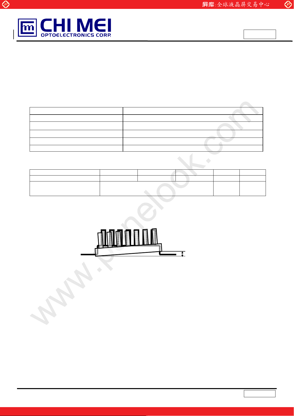
1.3 MECHANICAL SPECIFICATIONS (ME)
Item Min. Typ. Max. Unit Note
Weight 2260 2560 2860 g -
I/F connector mounting
position
Note (1) Please refer to the attached drawings for more information of front and back outline dimensions.
(2) Connector mounting position
The mounting inclination of the connector makes
the screen center within ±0.5mm as the horizontal.
+/- 0.5mm
(2)
4
One step solution for LCD / PDP / OLED panel application: Datasheet, inventory and accessory!
Versio n 1.0
www.panelook.com
Page 5
Global LCD Panel Exchange Center
www.panelook.com
Issued Date: Feb. 13, 2009
Model No.: V400H1-PH1
2. ABSOLUTE MAXIMUM RATINGS
2.1 ABSOLUTE RATINGS OF ENVIRONMENT (BASED ON CMO MODULE V400H1-PH1)
Item Symbol
Storage Temperature TST -20 +60 ºC (1), (3)
Operating Ambient Temperature TOP 0 50 ºC (1), (2), (3)
Altitude Operating A OP 0 5000 M (3)
Altitude Storage A ST 0 12000 M (3)
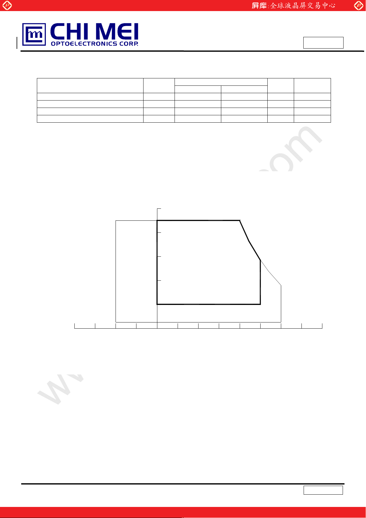
Note (1) Temperature and relative humidity range is shown in the figure below.
(a) 90 %RH Max. (Ta Љ 40 ºC).
(b) Wet-bulb temperature should be 39 ºC Max. (Ta > 40 ºC).
(c) No condensation..
Min. Max.
Value
Unit Note
Approval
Relative Humidity (%RH)
100
90
80
60
Operating Range
40
20
10
Storage Range
Temperature (ºC)
80 60 -20 40 0 20 -40
Note (2) The maximum operating temperature is based on the test condition that the surface temperature
of display area is less than or equal to 65 ºC with LCD module alone in a temperature controlled
chamber. Thermal management should be considered in your product design to prevent the
surface temperature of display area from being over 65 ºC. The range of operating temperature
may degrade in case of improper thermal management in your product design.
Note (3) The rating of environment is base on LCD module. Leave LCD cell alone, this environment condition
can’tbe guaranteed. Except LCD cell, the customer has to consider the ability of other parts of LCD
module and LCD module process.
5
One step solution for LCD / PDP / OLED panel application: Datasheet, inventory and accessory!
Versio n 1.0
www.panelook.com
Page 6
Global LCD Panel Exchange Center
www.panelook.com
2.2 ABSOLUTE RATINGS OF ENVIRONMENT (OPEN CELL)
Storage Condition : With shipping package.
Storage temperature range : 25±5 к
Storage humidity range : 50±10%RH
Shelf life : a month
2.3 ELECTRICAL ABSOLUTE RATINGS (OPEN CELL)
Issued Date: Feb. 13, 2009
Model No.: V400H1-PH1
Approval
Item Symbol
Power Supply Voltage Vcc -0.3 13.5 V
Input Signal Voltage VIN -0.3 3.6 V
Min. Max.
Value
Unit Note
(1)
6
One step solution for LCD / PDP / OLED panel application: Datasheet, inventory and accessory!
Versio n 1.0
www.panelook.com
Page 7

Global LCD Panel Exchange Center
3. ELECTRICAL CHARACTERISTICS
www.panelook.com
Issued Date: Feb. 13, 2009
Model No.: V400H1-PH1
Approval
3.1 TFT LCD MODULE
Parameter Symbol
Ta = 25 ± 2 ºC
Value
Min. Typ. Max.
Unit Note
Power Supply Voltage VCC 10.8 12.0 13.2 V (1)
Power Supply Ripple Voltage VRP - - 350 mV
Rush Current I
- - 4.5 A (2)
RUSH
White - 2.6 2.9 A
Power Supply Current
Common Input Voltage V
Interface
Terminating Resistor R
Black - 2 A
Vertical Stripe
I
CC
- 2.6 A
1.125 1.25 1.375 V LVDS
LVC
- 100 - ohm
T
(3)
Input High Threshold Voltage VIH 2.7 - 3.3 V CMOS
interface
Input Low Threshold Voltage V
0 - 0.7 V
IL
Note (1) The module should be always operated within above ranges.
Note (2) Measurement Conditions: (Base on V400H1-PH1 module)
+12V
R1
1K
Q1
Si4485D
FUSE
C3
1uF
Vcc
(LCD Module Input)
(Low to High)
(Control Signal)
SW
GND
VR1
47K
R2
1K
Q2
2N7002
Vcc rising time is 470us
0.9Vcc
0.1Vcc
470us
C1
0.01
Vcc
Note (3) The specified power supply current is under the conditions at Vcc = 12V, Ta = 25 ± 2 ºC, f
whereas a power dissipation check pattern below is displayed.
7
One step solution for LCD / PDP / OLED panel application: Datasheet, inventory and accessory!
= 60 Hz,
v
Versio n 1.0
www.panelook.com
Page 8

Global LCD Panel Exchange Center
www.panelook.com
Issued Date: Feb. 13, 2009
Model No.: V400H1-PH1
Approval
a. White Pattern
Active Area
c. Vertical Stripe Pattern
b. Black Pattern
Active Area
R
G
R
B
G
R
B
G
R R
G
B
B
B
B
R
R
R
G
G
G
G
B
B
B
B
R
R
Active Area
8
One step solution for LCD / PDP / OLED panel application: Datasheet, inventory and accessory!
Versio n 1.0
www.panelook.com
Page 9

Global LCD Panel Exchange Center
)
4. BLOCK DIAGRAM
4.1 TFT LCD MODULE
ODD_RIN0+/ODD_RIN1+/ODD_RIN2+/ODD_RIN3+/ODD_RIN4+/ODD_CLK+/-
EVEN_RIN0+/EVEN_RIN1+/EVEN_RIN2+/EVEN_RIN3+/EVEN_RIN4+/EVEN_CLK+/-
SCL_I
SDA_I
TCON_CHECK
TST_PGM
HSYNC
LVD S
I2C_SCL
FRE_NRESET
I2C_SDA
SW_PVCC
MAIN_CHECK
VIN
GND
INPUT CONNECTOR
(FI-RE51S-HF (JAE))
FRAME
BUFFER
FRC
www.panelook.com
FRAME
BUFFER
TIMING
CONTROLLER
DC/DC CONVERTER
& REFERENCE
VOLTAGE
GENERATOR
Issued Date: Feb. 13, 2009
Model No.: V400H1-PH1
Approval
SCAN DRIVER
TFT LCD PANEL
(1920x3x1080)
DATA DRIVER (RSDS
CN3-CN13 (Master): SM02-BDAS-3-TB (JST)
BALANCE BOARD
CONNECTOR
CN1 (LL):
SM02-BDAS-3-TB
(JST)
+(-) HV
CN33: KN 30-7P- 1.25H (Hirose)
BACKLIGHT
UNIT
IP board
BALANCE BOARD
CONNECTOR
CN1 (RL):
SM02-BDAS-3-TB
(JST)
-(+) HV
9
One step solution for LCD / PDP / OLED panel application: Datasheet, inventory and accessory!
Versio n 1.0
www.panelook.com
Page 10

Global LCD Panel Exchange Center
5. INPUT TERMINAL PIN ASSIGNMENT
5.1 TFT LCD Module Input
CN505 Connector Pin Assignment
Pin No. Symbol Description
1 VIN
2 VIN
3 VIN
4 VIN
5 VIN
6 NC No connection
7 GND
8 GND
9 GND
10 ODD_RIN0N
11 ODD_RIN0P
12 ODD_RIN1N
13 ODD_RIN1P
14 ODD_RIN2N
15 ODD_RIN2P
16 GND
17 ODD_RINCLKN
18 ODD_RINCLKP
19 GND
20 ODD_RIN3N
21 ODD_RIN3P
22 ODD_RIN4N
23 ODD_RIN4P
24 GND
25 EVEN_RIN0N
26 EVEN _RIN0P
27 EVEN _RIN1N
28 EVEN _RIN1P
29 EVEN _RIN2N
30 EVEN _RIN2P
31 GND
32 EVEN _RINCLKN
33 EVEN _RINCLKP
34 GND
35 EVEN _RIN3N
36 EVEN _RIN3P
37 EVEN _RIN4N
38 EVEN _RIN4P
39 GND
40 SCL_I SEC define
www.panelook.com
Issued Date: Feb. 13, 2009
Model No.: V400H1-PH1
Approval
+12.0V power supply
+12.0V power supply
+12.0V power supply
+12.0V power supply
+12.0V power supply
Ground
Ground
Ground
Negative transmission data of First pixel 0
Positive transmission data of First pixel 0
Negative transmission data of First pixel 1
Positive transmission data of First pixel 1
Negative transmission data of First pixel 2
Positive transmission data of First pixel 2
Ground
Negative of First clock
Positive of First clock
Ground
Negative transmission data of First pixel 3
Positive transmission data of First pixel 3
Negative transmission data of First pixel 4
Positive transmission data of First pixel 4
Ground
Negative transmission data of Second pixel 0
Positive transmission data of Second pixel 0
Negative transmission data of Second pixel 1
Positive transmission data of Second pixel 1
Negative transmission data of Second pixel 2
Positive transmission data of Second pixel 2
Ground
Negative of Second clock
Positive of Second clock
Ground
Negative transmission data of Second pixel 3
Positive transmission data of Second pixel 3
Negative transmission data of Second pixel 4
Positive transmission data of Second pixel 4
Ground
10
One step solution for LCD / PDP / OLED panel application: Datasheet, inventory and accessory!
Versio n 1.0
www.panelook.com
Page 11

Global LCD Panel Exchange Center
41 SDA_I SEC define
42 TCON_CHECK SEC define
43 TST_PGM SEC define
44 HSYNC SEC define
45 LVDS_SEL SEC define
46 I2C_SCL SEC define
47 FRC_NRESET SEC define
48 I2C_SDA SEC define
49 SW_PVCC SEC define
50 MAIN_CHECK SEC define
51 NC No connection
Note (1) CN505 Connector Part No.: JAE Taiwan (ሽ) FI-RE51S-HF or equal.
www.panelook.com
Issued Date: Feb. 13, 2009
Model No.: V400H1-PH1
Approval
11
One step solution for LCD / PDP / OLED panel application: Datasheet, inventory and accessory!
Versio n 1.0
www.panelook.com
Page 12

Global LCD Panel Exchange Center
5.2 BLOCK DIAGRAM OF INTERFACE
www.panelook.com
Issued Date: Feb. 13, 2009
Model No.: V400H1-PH1
Approval
12
One step solution for LCD / PDP / OLED panel application: Datasheet, inventory and accessory!
Versio n 1.0
www.panelook.com
Page 13

Global LCD Panel Exchange Center
5.3 LVDS INTERFACE
VESA Format : SELLVDS = H or Open
JEIDA Format : SELLVDS = L
www.panelook.com
Issued Date: Feb. 13, 2009
Model No.: V400H1-PH1
Approval
AR0~AR9: First Pixel R Data (9; MSB, 0; LSB)
AG0~AG9: First Pixel G Data (9; MSB, 0; LSB)
AB0~AB9: First Pixel B Data (9; MSB, 0; LSB)
DE : Data enable signal
DCLK : Data clock signal
RSVD : Reserved
13
One step solution for LCD / PDP / OLED panel application: Datasheet, inventory and accessory!
Versio n 1.0
www.panelook.com
Page 14

Global LCD Panel Exchange Center
5.4 COLOR DATA INPUT ASSIGNMENT
The brightness of each primary color (red, green and blue) is based on the 10-bit gray scale data input
for the color. The higher the binary input, the brighter the color. The table below provides the assignment
of color versus data input.
Color
Black
Red
Basic
Colors
Gray
Scale
Of
Red
Gray
Scale
Of
Green
Gray
Scale
Of
Blue
Green
Blue
Cyan
Magenta
Yel lo w
White
Red (0) / Dark
Red (1)
Red (2)
:
:
Red (1021)
Red (1022)
Red (1023)
Green (0) / Dark
Green (1)
Green (2)
:
:
Green (1021)
Green (1022)
Green (1023)
Blue (0) / Dark
Blue (1)
Blue (2)
:
:
Blue (1021)
Blue (1022)
Blue (1023)
Note (1) 0: Low Level Voltage, 1: High Level Voltage
R9 R8 R7 R6 R5 R4 R3 R2 R1 R0 G9 G8 G7 G6 G5 G4 G3 G2 G1 G0 B9 B8 B7 B6 B5 B4 B3 B2 B1 B0
0
0
0
1
0
0
0
1
1
1
0
0
0
1
1
1
0
0
0
:
:
0
0
0
0
0
0
:
:
0
0
0
0
1
1
1
0
0
0
0
0
0
0
0
0
1
1
1
1
1
1
1
1
1
0
0
0
0
0
0
0
0
0
:
:
:
:
1
1
1
1
1
1
1
1
1
0
0
0
0
0
0
0
0
0
:
:
:
:
:
:
0
0
0
0
0
0
0
0
0
0
0
0
0
0
0
0
0
0
:
:
:
:
:
:
0
0
0
0
0
0
0
0
0
www.panelook.com
Issued Date: Feb. 13, 2009
Model No.: V400H1-PH1
Approval
0
0
1
0
1
0
1
1
0
0
0
:
:
0
0
0
0
0
0
:
:
1
1
1
0
0
0
:
:
0
0
0
Data Signal
0
0
0
0
1
1
0
0
1
1
0
0
1
1
1
1
0
0
0
0
0
0
:
:
:
:
0
0
0
0
0
0
0
0
0
0
0
0
:
:
:
:
1
1
1
1
1
1
0
0
0
0
0
0
:
:
:
:
0
0
0
0
0
0
0
0
0
0
0
0
0
0
0
0
0
0
0
0
0
0
0
0
0
1
1
1
1
1
0
0
0
1
1
1
0
0
0
1
1
1
1
1
1
0
0
0
0
0
0
0
0
0
:
:
:
:
:
:
0
0
0
0
0
0
0
0
0
0
0
0
0
0
0
0
0
0
:
:
:
:
:
:
1
1
1
1
1
1
1
1
1
0
0
0
0
0
0
0
0
0
:
:
:
:
:
:
0
0
0
0
0
0
0
0
0
1
0
0
0
1
1
1
0
0
0
1
1
1
1
1
1
0
0
0
0
0
0
0
0
0
:
:
:
:
:
:
0
0
0
0
0
0
0
0
0
0
0
0
0
0
1
0
1
0
:
:
:
:
:
:
1
0
1
1
1
0
1
1
1
0
0
0
0
0
0
0
0
0
:
:
:
:
:
:
0
0
0
0
0
0
0
0
0
0
0
0
0
1
1
1
1
1
1
1
1
1
0
0
0
1
1
1
0
0
0
0
0
0
0
0
0
:
:
:
;
:
:
0
0
0
0
0
0
0
0
0
0
0
0
0
0
0
0
0
0
:
:
:
:
:
:
0
0
0
0
0
0
0
0
0
0
0
0
0
0
0
0
0
0
:
:
:
:
:
:
1
1
1
1
1
1
1
1
1
0
0
0
0
0
0
0
1
1
1
1
1
1
1
1
1
0
0
0
1
1
1
0
0
0
0
0
0
0
0
0
:
:
:
:
:
:
0
0
0
0
0
0
0
0
0
0
0
0
0
0
0
0
0
0
:
:
:
:
:
:
0
0
0
0
0
0
0
0
0
0
0
0
0
0
0
0
0
0
:
:
:
:
:
:
1
1
1
1
1
1
1
1
1
0
0
0
0
1
1
1
0
1
0
0
0
:
:
0
0
0
0
0
0
:
:
0
0
0
0
0
0
:
:
1
1
1
0
0
0
0
0
0
0
0
1
1
1
1
1
1
1
1
1
0
0
0
1
1
1
0
0
0
0
0
0
0
0
0
:
:
:
:
:
:
0
0
0
0
0
0
0
0
0
0
0
0
0
0
0
0
0
0
:
:
:
:
:
:
0
0
0
0
0
0
0
0
0
0
0
0
0
0
1
0
1
0
:
:
:
:
:
:
1
0
1
1
1
0
1
1
1
Red Green Blue
0
0
0
0
0
0
1
1
1
0
0
0
1
1
1
0
0
0
:
:
1
1
1
0
0
0
:
:
0
0
0
0
0
0
:
:
0
0
0
1
0
0
0
0
0
0
0
0
0
1
1
1
1
1
1
1
1
1
0
0
0
0
0
0
0
0
0
:
:
:
:
:
:
1
1
1
1
1
1
1
1
1
0
0
0
0
0
0
0
0
0
:
:
:
:
:
:
0
0
0
0
0
0
0
0
0
0
0
0
0
0
0
0
0
0
:
:
:
:
:
:
0
0
0
0
0
0
0
0
0
0
1
1
0
0
0
1
0
0
0
0
0
1
1
1
0
1
1
1
1
1
1
0
0
0
0
1
0
1
0
0
:
:
:
:
:
:
0
1
0
1
0
0
1
1
0
0
0
0
0
0
0
0
0
0
:
:
:
:
:
:
0
0
1
0
0
1
0
0
1
0
0
0
0
0
0
0
0
0
:
:
:
:
:
:
0
0
0
0
0
0
0
0
0
14
One step solution for LCD / PDP / OLED panel application: Datasheet, inventory and accessory!
Versio n 1.0
www.panelook.com
Page 15

Global LCD Panel Exchange Center
6. INTERFACE TIMING
6.1 INPUT SIGNAL TIMING SPECIFICATIONS
The input signal timing specifications are shown as the following table and timing diagram.
Signal Item Symbol Min. Typ. Max. Unit Note
LVDS Receiver Clock 1/Tc - 74 - MHZ
Hsync Fh - 67.5 - KHz
Vsync
Frequency
www.panelook.com
Issued Date: Feb. 13, 2009
Model No.: V400H1-PH1
Approval
Fv - 59.94 - Hz
LVDS Receiver Data
Vertical Active Display Term
Horizontal Active Display Term
.
Note: Since this control board is operated in Hsync and Vsync input signals should be set to low logic
level or ground. Otherwise, this module would operate abnormally.
.
6.2 INTERNAL SIGNAL TIMING SPECIFICATIONS (FRC T-CON)
The input signal timing specifications are shown as the following table and timing diagram.
Signal Item Symbol Min. Typ. Max. Unit Note
LVDS Receiver Clock 1/Tc 60 74 80 MHZ (1)
Hsync Fh - 135 - KHz
Vsync
Setup Time Tlvsu 600 - - ps
Hold Time Tlvhd 600 - - ps
Frame Rate
To ta l Tv - 1125 - Th Tv=Tvd+Tvb
Display Tvd Blank Tvb Total Th - 2200 - Tc Th=Thd+Thb
Display Thd - 1920 - Tc Blank
Thb - 280 - Tc -
Frequency
Fr6 57 60 63 Hz
1080
45
Fv - 120 - Hz
-Th -
-Th -
LVDS Receiver Data
Vertical Active Display Term
Horizontal Active Display Term
Note : Since the module is operated in DE only mode, and Hsync and Vsync input signals should be set to low
logic level. Otherwise, this module would operate abnormally.
Note (1) LVDS Clock should not over 80MHz even if H-total or V-total is in spec, and the frequency follows the
equation below.
Note (2) LVDS CLK= Frame rate * H-total * V-total
Setup Time Tlvsu 600 - - ps
Hold Time Tlvhd 600 - - ps
Frame Rate
To ta l Tv
Display Tvd
Blank Tvb
Tot a l T h
Display Thd
Blank
Thb
Fr6 - 120 - Hz
1115
1080 1080 1080
35 45 330
540
480
60
15
1125 1410 Th Tv=Tvd+Tvb
Th -
Th 550 663 Tc Th=Thd+Thb
480
70
480
183
Tc Tc -
Versio n 1.0
One step solution for LCD / PDP / OLED panel application: Datasheet, inventory and accessory!
www.panelook.com
Page 16

Global LCD Panel Exchange Center
DE
T
h
DCLK
www.panelook.com
INPUT SIGNAL TIMING DIAGRAM
T
v
T
vd
Issued Date: Feb. 10, 2009
Model No.: V400H1-PH1
Approval
T
vb
DE
DAT
T
hd
Valid display data (960
LVDS RECEIVER INTERFACE TIMING DIAGRAM
Tc
RXCLK+/-
RXn+/-
Tlvsu
Tlvhd
1T
14
One step solution for LCD / PDP / OLED panel application: Datasheet, inventory and accessory!
3T
14
5T
14
7T
14
16
9T
14
11T
14
13T
14
Versio n 2.0
www.panelook.com
Page 17

Global LCD Panel Exchange Center
P
6.2 POWER ON/OFF SEQUENCE
(Ta = 25 ± 2 ºC)
To prevent a latch-up or DC operation of LCD module, the power on/off sequence should be as the diagram below.
0V
0ЉT1Љ10ms
2
0ЉT
0ЉT
LVDS Signals
Љ50ms
3
Љ50ms
1000ms ЉT
4
0V
0.1V
CC
Power On
www.panelook.com
T
1
T
2
VA L I D
Issued Date: Feb. 10, 2009
Model No.: V400H1-PH1
Approval
0.1V
cc
T
3
T
4
0ЉT7ЉT2
8
0ЉT
ЉT3
T
T
7
8
Option Signals
(SELLVDS,EN_DCR
Backlight (Recommended)
1000msЉT
100msЉT
5
6
50%
T
5
Power ON/OFF Sequence
Note (1) The supply voltage of the external system for the module input should follow the definition of Vcc.
Note (2) Apply the lamp voltage within the LCD operation range. When the backlight turns on before the LCD operation
or the LCD turns off before the backlight turns off, the display may momentarily become abnormal screen.
50%
T
6
Note (3) In case of Vcc is in off level, please keep the level of input signals on the low or high impedance. If T2<0,that
maybe cause electrical overstress failure.
Note (4) T4 should be measured after the module has been fully discharged between power off and on period.
Note (5) Interface signal shall not be kept at high impedance when the power is on.
17
One step solution for LCD / PDP / OLED panel application: Datasheet, inventory and accessory!
Versio n 2.0
www.panelook.com
Page 18

Global LCD Panel Exchange Center
7. Mechanical Drawing
www.panelook.com
Issued Date: Feb. 10, 2009
Model No.: V400H1-PH1
Approval
18
One step solution for LCD / PDP / OLED panel application: Datasheet, inventory and accessory!
Versio n 2.0
www.panelook.com
 Loading...