


Global LCD Panel Exchange Center |
www.panelook.com |
Issued Date: Jan. 14, 2008
Model No.: V315B1 - L08
Approval
TFT LCD Approval Specification
MODEL NO.: V315B1 - L08


Customer: |
Approved by: |
Note: |
TVHD |
Approved By |
LY Chen |
QRA Dept. |
Product Development Div. |
Reviewed By |
WT Lin |
Tomy Chen |
LCD TV Marketing and Product Management Div. |
|
Prepared By |
Jim Ho |
WY Li |
|
1
Version2.0
One step solution for LCD / PDP / OLED panel application: Datasheet, inventory and accessory! www.panelook.com
Global LCD Panel Exchange Center |
www.panelook.com |
|
Issued Date: Jan. 14, 2008 |
|
Model No.: V315B1 - L08 |
|
Approval |
|
- CONTENTS - |
REVISION HISTORY |
------------------------------------------------------- 3 |
1. GENERAL DESCRIPTION |
------------------------------------------------------- 4 |
1.1OVERVIEW
1.2FEATURES
1.3APPLICATION
1.4GENERAL SPECIFICATIONS
1.5MECHANICAL SPECIFICATIONS
2. ABSOLUTE MAXIMUM RATINGS ------------------------------------------------------- |
5 |
2.1 ABSOLUTE RATINGS OF ENVIRONMENT
2.2 PACKAGE STORAGE
2.3 ELECTRICAL ABSOLUTE RATINGS 2.3.1 TFT LCD MODULE
2.3.2 BACKLIGHT UNIT
3. ELECTRICAL CHARACTERISTICS ------------------------------------------------------- |
7 |
3.1 TFT LCD MODULE |
|
3.2 BACKLIGHT INVERTER UNIT |
|
3.2.1 CCFL(Cold Cathode Fluorescent Lamp) CHARACTERISTICS |
|
3.2.2 INVERTER CHARACTERISTICS |
|
3.2.3 INVERTER INTERFACE CHARACTERISTICS |
|
4. BLOCK DIAGRAM ------------------------------------------------------- |
12 |
4.1 TFT LCD MODULE |
|
5. INTERFACE PIN CONNECTION ------------------------------------------------------- |
13 |
5.1 TFT LCD MODULE |
|
5.2 BACKLIGHT UNIT |
|
5.3 INVERTER UNIT |
|
5.4 BLOCK DIAGRAM OF INTERFACE |
|
5.5 LVDS INTERFACE |
|
5.6 COLOR DATA INPUT ASSIGNMENT |
|
6. INTERFACE TIMING ------------------------------------------------------- |
19 |
6.1INPUT SIGNAL TIMING SPECIFICATIONS
6.2POWER ON/OFF SEQUENCE 

7. OPTICAL CHARACTERISTICS ------------------------------------------------------- |
22 |
7.1TEST CONDITIONS


7.2OPTICAL SPECIFICATIONS
8. DEFINITION OF LABELS ------------------------------------------------------- |
26 |
8.1 CMO MODULE LABE |
|
9. PACKAGING ------------------------------------------------------- |
27 |
9.1PACKING SPECIFICATIONS
9.2PACKING METHOD
10. PRECAUTIONS ------------------------------------------------------- |
29 |
10.1ASSEMBLY AND HANDLING PRECAUTIONS
10.2SAFETY PRECAUTIONS
10.3REGULATORY STANDARDS
11. MECHANICAL CHARACTERISTICS ------------------------------------------------------- |
30 |
2
Version2.0
One step solution for LCD / PDP / OLED panel application: Datasheet, inventory and accessory! www.panelook.com
Global LCD Panel Exchange Center |
www.panelook.com |
Issued Date: Jan. 14, 2008
Model No.: V315B1 - L08
Approval
REVISION HISTORY
Page
Version Date Section Description
(New)
Ver 2.0 |
Jan.14,’08 |
All |
All |
Approval Specification was first issued. |
|
|
|
|
|
3
Version2.0
One step solution for LCD / PDP / OLED panel application: Datasheet, inventory and accessory! www.panelook.com

Global LCD Panel Exchange Center |
www.panelook.com |
Issued Date: Jan. 14, 2008
Model No.: V315B1 - L08
Approval
1. GENERAL DESCRIPTION
1.1 OVERVIEW
V315B1L08 is a 31.5” TFT Liquid Crystal Display module with 16CCFL Backlight unit and 1ch-LVDS
interface. This module supports 1366 x 768 WXGA format and can display true 16.7M colors ( 8-bit colors).
The inverter module for backlight is built-in.
1.2 FEATURES
-High brightness (500 nits)
- Ultra-high contrast ratio (1800:1)
- Faster response time (gray to gray average 7.5ms)
- High color saturation NTSC 72%
- Ultra wide viewing angle : 176(H)/176(V) (CR 20) with Super MVA technology


- DE (Data Enable) only mode
- LVDS (Low Voltage Differential Signaling) interface
- 180 degree rotation display (option)
- Color reproduction (nature color)
- Low color shift function
- RoHS Compliance
1.3 APPLICATION
- TFT LCD TVs
- Multi-Media Display
1.4 GENERAL SPECIFICATI0NS


Item |
Specification |
Unit |
Note |
|
Active Area |
697.6845 (H) x 392.256 (V) (31.51" diagonal) |
mm |
(1) |
|
Bezel Opening Area |
703.8 (H) x 398.4 (V) |
mm |
||
|
||||
Driver Element |
a-si TFT active matrix |
- |
|
|
Pixel Number |
1366 x R.G.B. x 768 |
pixel |
|
|
Pixel Pitch (Sub Pixel) |
0.17025(H) x 0.51075 (V) |
mm |
|
|
Pixel Arrangement |
RGB vertical stripe |
- |
|
|
Display Colors |
16.7M |
color |
|
|
Display Operation Mode |
Transmissive mode / Normally black |
- |
|
|
Surface Treatment |
Anti-Glare coating (Haze17%),Hard coating (3H) |
- |
|
1.5 MECHANICAL SPECIFICATIONS
|
Item |
Min. |
Typ. |
Max. |
Unit |
Note |
|
|
|
Horizontal(H) |
759 |
760 |
761 |
mm |
(1) |
Module Size |
|
Vertical(V) |
449 |
450 |
451 |
mm |
(1) |
|
Depth(D) |
39 |
40 |
41 |
mm |
To PCB cover |
|
|
|
||||||
|
|
Depth(D) |
49.2 |
50.2 |
51.2 |
mm |
To inverter cover |
|
Weight |
-- |
6700 |
-- |
g |
|
|
Note (1) Please refer to the attached drawings for more information of front and back outline dimensions.
4
Version2.0
One step solution for LCD / PDP / OLED panel application: Datasheet, inventory and accessory! www.panelook.com
Global LCD Panel Exchange Center |
www.panelook.com |
Issued Date: Jan. 14, 2008
Model No.: V315B1 - L08
Approval
2.ABSOLUTE MAXIMUM RATINGS
2.1ABSOLUTE RATINGS OF ENVIRONMENT
Item |
Symbol |
|
Value |
Unit |
Note |
|
Min. |
|
Max. |
||||
|
|
|
|
|
||
Storage Temperature |
TST |
-20 |
|
+60 |
ºC |
(1) |
Operating Ambient Temperature |
TOP |
0 |
|
+50 |
ºC |
(1), (2) |
Shock (Non-Operating) |
SNOP |
- |
|
50 |
G |
(3), (5) |
Vibration (Non-Operating) |
VNOP |
- |
|
1.0 |
G |
(4), (5) |
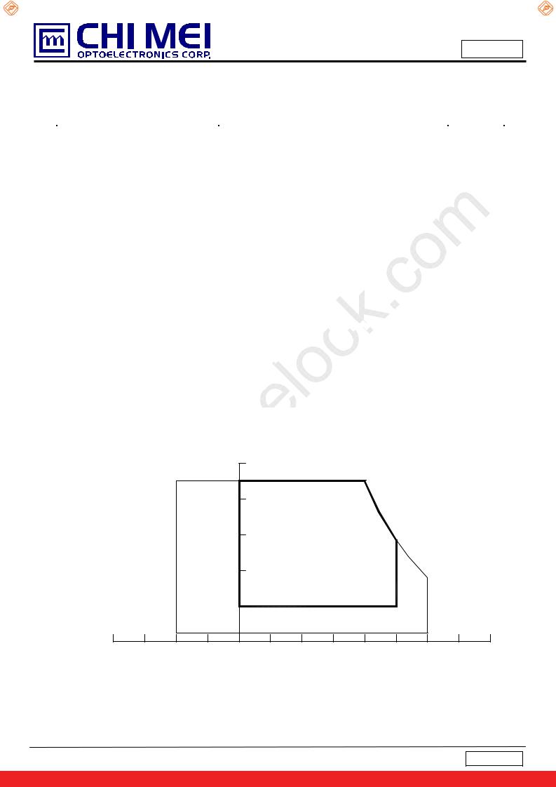
Note (1) Temperature and relative humidity range is shown in the figure below.
(a) 90 %RH Max. (Ta 40 ºC).
(b) Wet-bulb temperature should be 39 ºC Max. (Ta > 40 ºC).
(c) No condensation.
Note (2) The maximum operating temperature is based on the test condition that the surface temperature of display area is less than or equal to 65 ºC with LCD module alone in a temperature controlled chamber. Thermal management should be considered in final product design to prevent the surface temperature of display area from being over 65 ºC. The range of operating temperature may degrade in case of improper thermal management in final product design. 


Note (3) 11 ms, half sine wave, 1 time for ± X, ± Y, ± Z. Note (4) 10 ~ 200 Hz, 10 min, 1 time each X, Y, Z. 
Note (5) At testing Vibration and Shock, the fixture in holding the module has to be hard and rigid enough so that the module would not be twisted or bent by the fixture.
|
|
Relative Humidity (%RH) |
|
|
|
|
|
|
100 |
|
|
|
|
|
|
90 |
|
|
|
|
|
|
80 |
|
|
|
|
|
|
60 |
Operating Range |
|
|
|
|
|
|
|
|
|
|
|
|
40 |
|
|
|
|
|
|
20 |
|
|
|
|
|
|
10 |
Storage Range |
|
|
|
|
|
|
|
|
|
|
-40 |
-20 |
0 |
20 |
40 |
60 |
80 |
|
|
|
Temperature (ºC) |
|
|
|
|
|
|
5 |
|
|
|
|
|
|
|
|
|
Version2.0 |
One step solution for LCD / PDP / OLED panel application: Datasheet, inventory and accessory! www.panelook.com
Global LCD Panel Exchange Center |
www.panelook.com |
Issued Date: Jan. 14, 2008
Model No.: V315B1 - L08
Approval
2.2 Package storage
When storing modules as spares for a long time, the following precaution is necessary.
(a)Do not leave the module in high temperature, and high humidity for a long time. It is highly recommended to store the module with temperature from 0 to 35 at normal humidity without condensation.
(b)The module shall be stored in dark place. Do not store the TFT-LCD module in direct sunlight or fluorescent light.
2.3ELECTRICAL ABSOLUTE RATINGS
2.3.1 TFT LCD MODULE
Item |
Symbol |
|
Value |
Unit |
Note |
|
Min. |
Max. |
|||||
|
|
|
|
|||
Power Supply Voltage |
Vcc |
-0.3 |
13.0 |
V |
(1) |
|
Input Signal Voltage |
VIN |
-0.3 |
3.6 |
V |
||
|
2.3.2 BACKLIGHT UNIT
Item |
Symbol |
|
Value |
Unit |
Note |
|
Min. |
Max. |
|||||
Lamp Voltage |
VW |
|
|
|||
|
3000 |
VRMS |
|
|||
Power Supply Voltage |
VBL |
0 |
30 |
V |
(1) |
|
Control Signal Level |
|
-0.3 |
7 |
V |
(1), (3) |
Note (1) Permanent damage to the device may occur if maximum values are exceeded. Functional
operation should be restricted to the conditions described under normal operating conditions. Note (2) No moisture condensation or freezing.


Note (3) The control signals includes Backlight On/Off Control, I_PWM Control, E_PWM Control and ERR signal for inverter status output. 


6
Version2.0
One step solution for LCD / PDP / OLED panel application: Datasheet, inventory and accessory! www.panelook.com
Global LCD Panel Exchange Center |
www.panelook.com |
|
|
|
|
|
|
Issued Date: Jan. 14, 2008 |
||
|
|
|
|
|
|
|
Model No.: V315B1 - L08 |
|
|
|
|
|
|
|
|
|
Approval |
3. ELECTRICAL CHARACTERISTICS |
|
|
|
|
|
|
||
3.1 TFT LCD MODULE |
|
|
|
|
|
Ta = 25 ± 2 ºC |
||
|
Parameter |
Symbol |
|
Value |
|
Unit |
Note |
|
|
Min. |
Typ. |
Max. |
|||||
|
|
|
|
|
|
|||
Power Supply Voltage |
|
VCC |
11.4 |
12.0 |
12.6 |
V |
(1) |
|
Power Supply Ripple Voltage |
VRP |
- |
- |
100 |
mV |
|
||
Rush Current |
White |
IRUSH |
- |
- |
4.3 |
A |
(2) |
|
Power Supply Current |
ICC |
- |
0.6 |
0.76 |
A |
(3) |
||
Black |
- |
0.28 |
- |
A |
||||
|
|
Vertical Stripe |
|
- |
0.54 |
- |
A |
|
|
Differential Input High |
VLVTH |
- |
- |
+100 |
mV |
|
|
LVDS |
Threshold Voltage |
|
||||||
|
|
|
|
|
|
|||
Differential Input Low |
|
-100 |
- |
- |
mV |
|
||
Interface |
VLVTL |
|
||||||
Threshold Voltage |
|
|||||||
|
Common Input Voltage |
VLVC |
1.125 |
1.25 |
1.375 |
V |
|
|
|
Terminating Resistor |
RT |
- |
100 |
- |
ohm |
|
|
CMOS |
Input High Threshold Voltage |
VIH |
2.7 |
- |
3.3 |
V |
|
|
interface |
Input Low Threshold Voltage |
VIL |
0 |
- |
0.7 |
V |
|
|
Note (1) The module should be always operated within above ranges.


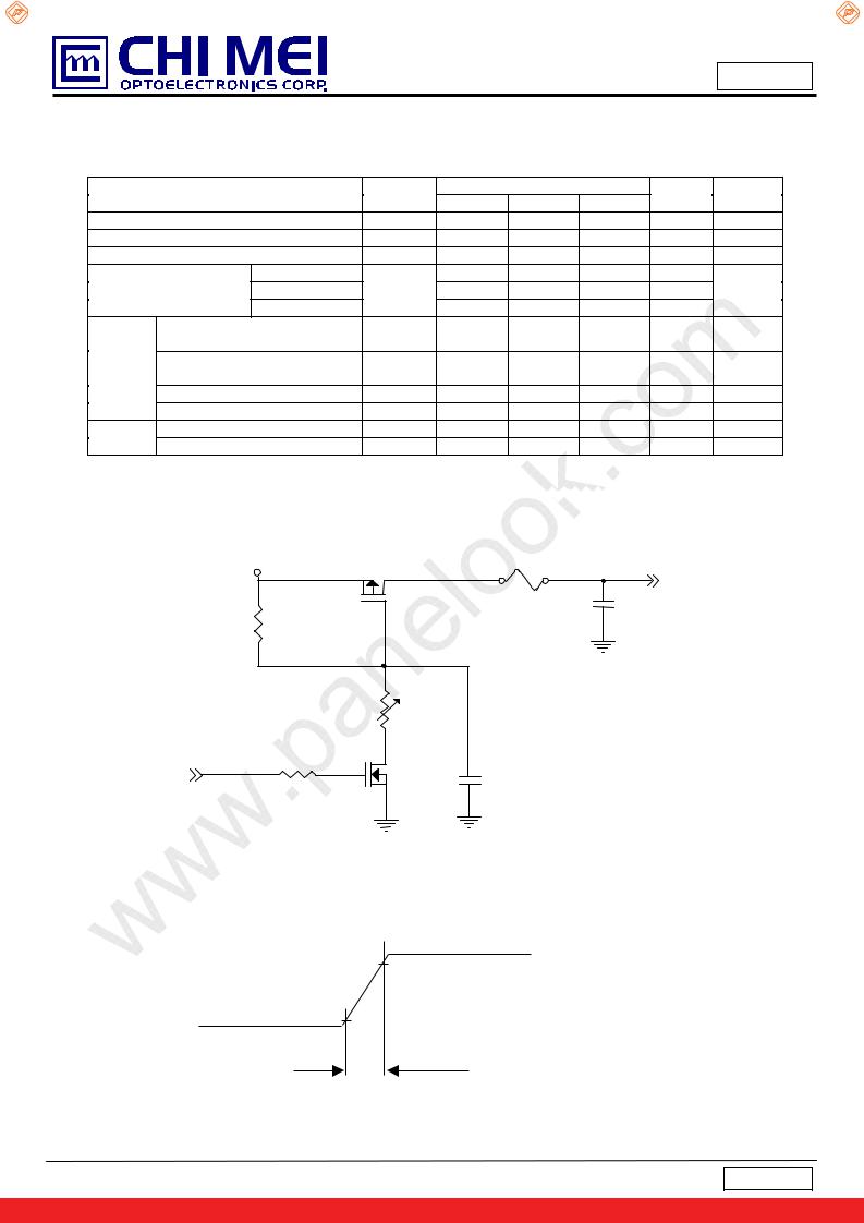
Note (2) Measurement Conditions:
|
+12.0V |
|
|
|
|
Q1 |
Si4435DY |
|
|
|
|
|
|
Vcc |
|
|
|
FUSE |
C3 |
|
|
|
(LCD Module Input) |
|
|
R1 |
|
|
1uF |
|
1K |
|
|
|
|
|
VR1 |
|
|
|
|
47K |
|
|
(Low to High) |
|
|
|
|
(Control Signal) |
R2 |
|
|
|
Follow CMOS interface |
Q2 |
C1 |
|
|
SW |
|
|
||
|
|
|
||
|
|
|
|
|
|
1K |
2N7002 |
|
|
|
|
0.01uF |
|
|
|
|
|
|
Vcc rising time is 470us
+12V
0.9Vcc
0.1Vcc
GND
470us
7
Version2.0
One step solution for LCD / PDP / OLED panel application: Datasheet, inventory and accessory! www.panelook.com
Global LCD Panel Exchange Center |
www.panelook.com |
Issued Date: Jan. 14, 2008
Model No.: V315B1 - L08
Approval
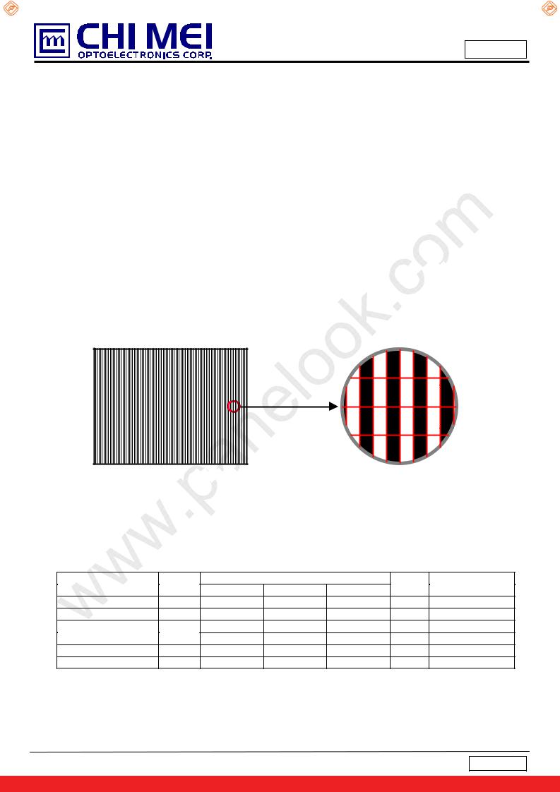
Note (3) The specified power supply current is under the conditions at Vcc = 12 V, Ta = 25 ± 2 ºC, fv = 60 Hz,
whereas a power dissipation check pattern below is displayed.
a. White Pattern |
b. Black Pattern |
|
|
|
|
|
|
|
Active Area
c. Vertical Stripe Pattern
Active Area


Active Area

R G B R G B |
B R G B R G B R |
B R G B R G B R |
R G B R G B |
3.2BACKLIGHT INVERTER UNIT
3.2.1CCFL (Cold Cathode Fluorescent Lamp) CHARACTERISTICS (Ta = 25 ± 2 ºC)
Parameter |
Symbol |
|
Value |
|
Unit |
Note |
|
Min. |
Typ. |
Max. |
|||||
Lamp Voltage |
VW |
VRMS |
IL = 7.6mA |
||||
- |
1050 |
- |
|||||
Lamp Current |
IL |
7.1 |
7.6 |
8.1 |
mARMS |
(1)High volt side |
|
Lamp Starting Voltage |
VS |
- |
- |
TBD |
VRMS |
(2), Ta = 0 ºC |
|
- |
1250 |
|
VRMS |
(2), Ta = 25 ºC |
|||
|
|
|
|||||
Operating Frequency |
FO |
40 |
- |
70 |
KHz |
(3) |
|
Lamp Life Time |
LBL |
50,000 |
|
- |
Hrs |
(4) |
8
Version2.0
One step solution for LCD / PDP / OLED panel application: Datasheet, inventory and accessory! www.panelook.com
Global LCD Panel Exchange Center |
www.panelook.com |
Issued Date: Jan. 14, 2008
Model No.: V315B1 - L08
Approval
3.2.2 INVERTER CHARACTERISTICS (Ta = 25 ± 2 ºC)
Parameter |
Symbol |
|
|
|
Value |
|
|
|
Unit |
|
Note |
||
|
Min. |
|
Typ. |
Max. |
|
|
|||||||
|
|
|
|
|
|
|
|
|
|||||
Power Consumption |
PBL |
- |
|
106 |
|
110 |
|
W |
(5),(6), IL = 7.6mA |
||||
Input Voltage |
VBL |
22.8 |
|
24 |
|
25.2 |
|
VDC |
|
|
|||
Input Current |
IBL |
- |
|
4.42 |
|
- |
|
|
A |
Non Dimming |
|||
Input Ripple Noise |
- |
- |
|
- |
|
912 |
|
mVP-P |
VBL=22.8V |
||||
Oscillating Frequency |
FW |
55 |
|
58 |
|
61 |
|
kHz |
|
|
|||
Dimming frequency |
FB |
130 |
|
150 |
|
170 |
|
Hz |
|
|
|||
Minimum Duty Ratio |
DMIN |
- |
|
20 |
|
- |
|
|
% |
(7) |
|||
Note (1) Lamp current is measured by utilizing high frequency current meters as shown below: |
|||||||||||||
|
|
|
|
HV (Pink) |
|
|
A |
|
|
|
|
|
|
|
|
|
|
|
1 |
|
|
|
|
|
|||
|
|
|
|
|
|
|
|
|
|
|
|
||
|
|
|
|
HV (White) |
|
2 |
A |
|
|
|
|
|
|
|
|
|
|
HV (Pink) |
|
|
|
|
|
|
|||
|
|
|
|
|
|
|
|
|
|
|
|
||
|
|
|
|
|
|
|
|
|
|
|
|
||
|
|
|
|
|
1 |
A |
|
|
|
|
|
||
|
|
|
|
|
|
|
|
|
|
|
|
||
|
|
|
|
HV (White) |
|
2 |
A |
|
|
|
|
|
|
|
|
|
|
HV (Pink) |
|
|
|
|
|
|
|||
|
|
|
|
|
|
|
|
|
|
|
|
||
|
|
|
|
|
|
|
|
|
|
|
|
||
|
|
|
|
|
1 |
A |
|
|
|
|
|
||
|
|
|
|
|
|
|
|
|
|
|
|
||
|
|
|
|
HV (White) |
|
2 |
|
|
|
|
|
|
|
|
|
|
|
|
|
|
A |
|
|
|
|
|
|
|
|
|
|
|
|
|
|
|
|
|
|
|
|
|
|
|
|
HV (Pink) |
|
|
|
|
|
|
|
|
|
|
|
|
|
|
1 |
A |
|
|
|
|
|
||
|
|
|
|
|
|
|
|
|
|
|
|
||
|
LCD |
|
|
HV (White) |
|
2 |
A |
|
Inverter |
|
|
||
|
Module |
|
HV (Pink) |
|
|
|
|
||||||
|
|
|
|
|
|
|
|
|
|
||||
|
|
|
1 |
A |
|
|
|
|
|
||||
|
|
|
|
|
|
|
|
|
|
|
|
||
|
|
|
|
HV (White) |
|
2 |
A |
|
|
|
|
|
|
|
|
|
|
HV (Pink) |
|
|
|
|
|
|
|||
|
|
|
|
|
|
|
|
|
|
|
|
||
|
|
|
|
|
|
|
|
|
|
|
|
||
|
|
|
|
|
1 |
A |
|
|
|
|
|
||
|
|
|
|
|
|
|
|
|
|
|
|
||
|
|
|
|
HV (White) |
|
2 |
|
|
|
|
|
|
|
|
|
|
|
|
|
|
A |
|
|
|
|
|
|
|
|
|
|
|
|
|
|
|
|
|
|
|
|
|
|
|
|
HV (Pink) |
|
|
A |
|
|
|
|
|
|
|
|
|
|
1 |
|
|
|
|
|
||||
|
|
|
|
|
|
|
|
|
|
|
|
||
|
|
|
|
HV (White) |
|
|
|
|
|
||||
|
|
|
|
|
2 |
A |
|
|
|
|
|
||
|
|
|
|
HV (Pink) |
|
|
|
|
|
|
|||
|
|
|
|
|
|
A |
|
|
|
|
|
||
|
|
|
|
1 |
|
|
|
|
|
||||
|
|
|
|
|
|
|
|
|
|
|
|
||
|
|
|
|
HV (White) |
|
|
|
|
|
|
|||
|
|
|
|
|
2 |
A |
|
|
|
|
|
||
|
|
|
|
|
|
|
|
|
|
|
|
||
|
|
|
|
|
|
|
|
|
|
|
|
|
|
Note (2) The lamp starting voltage VS should be applied to the lamp for more than 1 second under starting

 up duration. Otherwise the lamp could not be lighted on completed.
Note (3) The lamp frequency may produce interference with horizontal synchronous frequency of the 

 display input signals, and it may result in line flow on the display. In order to avoid interference, the lamp frequency should be detached from the horizontal synchronous frequency and its harmonics as far as possible.
Note (4) The life time of a lamp is defined as when the brightness is larger than 50% of its original value and the effective discharge length is longer than 80% of its original length (Effective discharge length is defined as an area that has equal to or more than 70% brightness compared to the brightness at the center point of lamp.) as the time in which it continues to operate under the
9
Version2.0
One step solution for LCD / PDP / OLED panel application: Datasheet, inventory and accessory! www.panelook.com

Global LCD Panel Exchange Center |
www.panelook.com |
Issued Date: Jan. 14, 2008
Model No.: V315B1 - L08
Approval
condition at Ta = 25 2 and IL =7.1 ~ 8.1 mARMS.
Note (5) The power supply capacity should be higher than the total inverter power consumption PBL. Since the pulse width modulation (PWM) mode was applied for backlight dimming, the driving current changed as PWM duty on and off. The transient response of power supply should be considered for the changing loading when inverter dimming.
Note (6) The measurement condition of Max. value is based on 31.5" backlight unit under input voltage 24V, average lamp current 7.9 mA and lighting 30 minutes later. 


Note (7) Minimum Duty Ration can support 10%, but accept flicker.
3.2.3 INVERTER INTERFACE CHARACTERISTICS
No |
ITEM |
SYMBOL |
TEST |
MIN |
TYPE |
MAX |
UNIT |
NOTE(1-2) |
|
CONDITION |
|||||||||
|
|
|
|
|
|
|
|
||
1 |
Error Signal |
ERR |
|
|
|
|
|
(Note 2) |
|
2 |
ON |
|
|
2.0 |
|
5.0 |
V |
|
|
On/Off Control Voltage |
VBLON |
|
0 |
|
0.8 |
V |
|
||
|
OFF |
|
|
|
|
||||
3 |
MAX |
VIPWM |
|
3.15 |
3.3 |
3.45 |
V |
Maximum Duty Ratio |
|
Internal PWM Control Voltage |
|
|
0 |
|
V |
Minimum Duty Ratio |
|||
|
MIN |
|
|||||||
4 |
HI |
VEPWM |
|
2.0 |
|
5.0 |
V |
ON Duration |
|
External PWM Control Voltage |
|
0 |
|
0.8 |
V |
OFF Duration |
|||
|
LO |
|
|
||||||
5 |
VBL Rising Time |
Tr1 |
|
30 |
|
50 |
ms |
|
|
6 |
VBL Falling Time |
Tf1 |
|
30 |
|
50 |
ms |
|
|
7 |
Control Signal Rising Time |
Tr |
|
|
|
100 |
ms |
|
|
8 |
Control Signal Falling Time |
Tf |
|
|
|
100 |
ms |
|
|
9 |
PWM Signal Rising Time |
TPWMR |
|
|
|
50 |
us |
|
|
10 |
PWM Signal Falling Time |
TPWMF |
|
|
|
50 |
us |
|
|
11 |
Input impedance |
RIN |
|
1 |
|
|
M |
|
|
12 |
PWM Delay Time |
TPWM |
|
100 |
|
300 |
mS |
|
|
13 |
BLON Delay Time |
Ton |
|
300 |
|
500 |
mS |
|
|
14 |
BLON Off Time |
TOFF |
|
300 |
|
500 |
mS |
|
Note (1) The power sequence and control signal timing are shown as the following figure 1.
Note (2) When inverter protective function is triggered, ERR will output open collector status; In normal operation, the signal of ERR will output a low level voltage.
10
Version2.0
One step solution for LCD / PDP / OLED panel application: Datasheet, inventory and accessory! www.panelook.com
 Loading...