

Page 1
Issued Date: 8/11/2004
Model No.: V370H1 – L01
Preliminary
TFT LCD Preliminary Specification
MODEL NO.: V370H1 - L01
LCD TV Division
AVP
郭振隆
Liquid Crystal Display Division
QRA Dept .
DDIII DDII DDI
Approval Approval Approval Approval
陳永一 李汪洋 藍文錦 林文聰
LCD TV Marketing and Project Management Dept.
TVHD/PDD
Product Manager
胡崇銘 吳文村
1 / 34
The information described in this technical specification is tent ative and it is possible to be changed witho ut prior notice.
Please contact CMO ’s represent ative while your product design is based on this specification. Version 0.2
Page 2

Issued Date: 8/11/2004
Model No.: V370H1 – L01
Preliminary
- CONTENTS -
REVISION HISTORY ------------------------------------------------------- 3
1. GENERAL DESCRIPTION ------------------------------------------------------- 4
1.1 OVERVIEW
1.2 FEATURES
1.3 APPLICATION
1.4 GENERAL SPECIFICATI0NS
1.5 MECHANICAL SPECIFICATIONS
2. ABSOLUTE MAXIMUM RATINGS ------------------------------------------------------- 5
2.1 ABSOLUTE RATINGS OF ENVIRONMENT
2.2 ELECTRICAL ABSOLUTE RATINGS
2.2.1 TFT LCD MODULE
2.2.2 BACKLIGHT INVERTER UNIT
3. ELECTRICAL CHARAC TERISTICS -------------------------- ----------------------------- 7
3.1 TFT LCD MODULE
3.2 BACKLIGHT UNIT
3.2.1 CCFL CHARACTERISTICS
3.2.2 INVERTER CHARACTERISTICS
3.2.3 INVERTER INTERTFACE CHARACTERISTIC
4. BLOCK DIAGRAM ---------------------------------------------- --------- 12
4.1 TFT LCD MODULE
5. INTERFACE PIN CONNECTION -------------------------- ----------------------------- 13
5.1 TFT LCD MODULE
5.2 BACKLIGHT UNIT
5.3 INVERTER UNIT
5.4 BLOCK DIAGRAM OF INTERFACE
5.5 LVDS INTERFACE
5.6 COLOR DATA INPUT ASSIGNMENT
6. INTERFACE TIMING -------------------------- ----------------------------- 21
6.1 INPUT SIGNAL TIMING SPECIFICATIONS
6.2 POWER ON/OFF SEQUENCE
7. OPTICAL CHARACTERISTICS ------------------------------------------------------- 24
7.1 TEST CONDITIONS
7.2 OPTICAL SPECIFICATIONS
8. DEFINITION OF LABELS ------------------------------------------------------- 28
8.1 CMO MODULE LABEL
9. PACKAGING ---------------------------------------------------- --- 29
9.1 PACKING SPECIFICATIONS
9.2 PACKING METHOD
10. PRECAUTIONS ------------------------------------------------------- 31
10.1 ASSEMBLY AND HANDLING PRECAUTIONS
10.2 SAFETY PRECAUTIONS
11. MECHANICAL CHARACTERISTIC ---------------------------- --------------------------- 32
2 / 34
The information described in this technical specification is tent ative and it is possible to be changed witho ut prior notice.
Please contact CMO ’s represent ative while your product design is based on this specification. Version 0.2
Page 3
Version Date
Ver 0.1
Ver.0.2
July.6,’04
Aug.11,’04
Page
(New)
All
10
11
12
13
14
16
24
25
26
27
32
33
34
Section Description
All
4
6
7
8
9
1.5
2.2.2
3.1
3.2.1
3.2.2
3.2.3
4.1
5.1
5.3
7.1
7.2
11
Issued Date: 8/11/2004
Model No.: V370H1 – L01
Preliminary
REVISION HISTORY
Preliminary Specification was first issued.
Module Size Depth(D) To PCB Cover: Min. 42.54Æ 43.34
Typ. 43.54Æ44.34
Max. 44.54Æ45.34
Note(3) The control signals includes On/Off Control, Internal PWM Control,
External PWM Control and Internal/External PWM Selection.Æ The control
signals includes Inverter Good, On/Off Control, Internal PWM Control, External
PWM Control and Internal/External PWM Selection.
Rush Current: I
Lamp Input Voltage: V
Note I
Lamp Current: I
Typ. 5.5Æ 4.8
Max. 6.0Æ 5.3
Lamp Turn On Voltage: V
Power consumption: P
Note(5), I
Note (4) I
= 5.5mAÆ 4.8mA
L
= 5.0 ~ 6.0 mArmsÆ 4.3 ~ 5.3 mArms
L
Add Parameter “Inverter Good Signal”
Internal PWM Control Voltage: (MAX.) Symbol V
(MIN.) Symbol V
Update Note (2)
Update “TFT LCD MODULE”
J1 Connector Pin AssignmentÆ CNF2 Connector Pin Assignment
Note (2) J1 Connector part no.: 53261-1519 (Molex) or equivalentÆ
Note (2) CNF2 Connector part no.: 53261-1519 (Molex) or equivalent.
INVERTER UNIT: Update CN1 table
Lamp Current: I
The following items should be measured under the test conditions describ ed in
7.1 and stable environment shown in Note (7)Æ Note (6)
Response time: Delete Symbol T
Color Chromaticity: Green Gy Typ.(0.604)Æ (0.598)
Blue Bx Typ.(0.410)Æ (0.412)
By Ty p.(0 .076 )Æ (0.072)
Add Note (6)
Delete Note 9300K
Delete Note (3) Definition of Response Time (T
Update Note (3) Definition of Gray to Gray Switching Time
Update Note (4)
Update Note (5)
Update Note (6)
Update Note (7)
Update MECHANICAL CHARACTERISTIC
Typ. 4.5Æ 2
RUSH
L
Min. 5.0Æ 4.3
L
Typ. 0Æ -
IPWM
Max.-Æ 3.0
5.5±0.5Æ 4.8±0.5
L
Gray to gray average: Note (4)Æ Note (3)
Typ. 1200Æ 1300
= 5.5 mA Æ (4.8)mA
L
Max. 2780Æ 2440
S
Typ. 160Æ 150
BL
CN2 : Pin No. 4~6
R, TF
Typ.-Æ 0
IPWM
Max. 3.0Æ -
, TF)
R
3 / 34
The information described in this technical specification is tent ative and it is possible to be changed witho ut prior notice.
Please contact CMO ’s represent ative while your product design is based on this specification. Version 0.2
Page 4
Issued Date: 8/11/2004
Model No.: V370H1 – L01
Preliminary
1. GENERAL DESCRIPTION
1.1 OVERVIEW
V370H1-L01 is a 37” TFT Liquid Crystal Display module with 20-CCFL Backlight unit and 2ch-LVDS interface.
This module supports 1920 x 1080 HDT V format and can display true 16.7M colors ( 8 -bit/color). The inverter
module for backlight is build-in.
1.2 FEATURES
- High brightness ( 550 nits)
- High contrast ratio (>600:1)
- Fast response time
- High color saturation NTSC 75%
- HDTV (1920 x 1080 pixels) resolution, true HDTV format .
- DE (Data Enable) only mode
- LVDS (Low Volt age Differential Signaling) interface
- Optimized response time for 50/60Hz frame rate
- Ultra wide viewing angle : 176(H)/176(V) (CR>20) Super MVA technology
- 180 degree rotation display option
1.3 APPLICA TION
- TFT LCD TVs
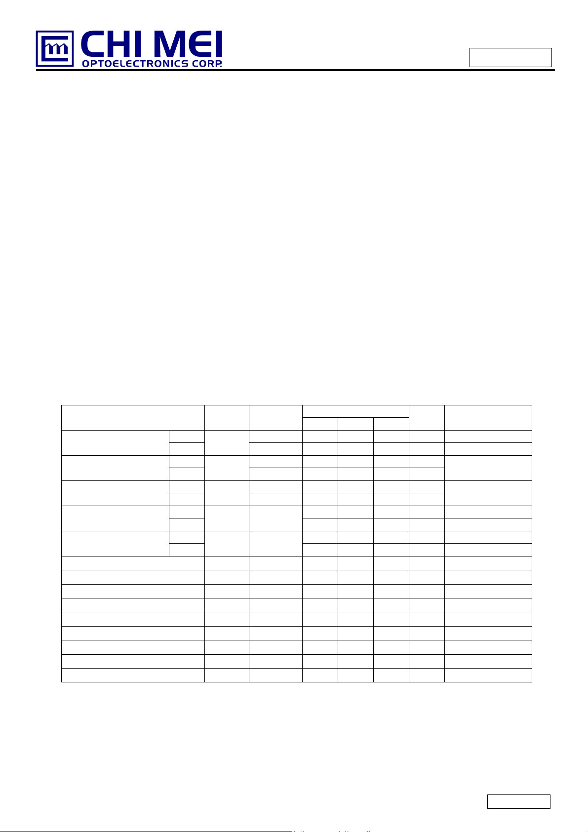
1.4 GENERAL SPECIFICATI0NS
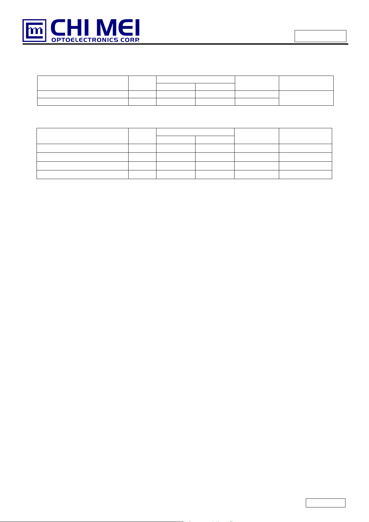
Item Specification Unit Note
Active Area 820.8(H) x 461.7 (V) (37.07” diagonal) mm
Bezel Opening Area 828.8 (H) x 470.9 (V) mm
Driver Element a-si TFT active matrix -
Pixel Number 1920 x R.G.B. x 1080 pixel
Pixel Pitch (Sub Pixel) 0.1425 (H) x 0.4275 (V) mm
Pixel Arrangement RGB vertical stripe -
Display Colors 16.7M color
Display Operation Mode Transmissive mode / Normally black -
Surface Treatment
Anti-reflective coating < less 2% reflection
Hardness (3H), Haze : 40%
(1)
-
1.5 MECHANICAL SPECIFICATIONS
Item Min. Typ. Max. Unit Note
Horizontal(H) 884.1 884.8 885.5 mm
Module Size
Note (1) Please refer to the attached drawings for more information of front and back outline dimensions.
The information described in this technical specification is tent ative and it is possible to be changed witho ut prior notice.
Please contact CMO ’s represent ative while your product design is based on this specification. Version 0.2
Vertical(V) 525.4 525.9 526.4 mm
Depth(D) 43.34 44.34 45.34 mm To PCB cover
Depth(D) 50.74 52.24 53.74 mm To inverter cover
Weight 8950 9150 9350 g
4 / 34
Page 5
Issued Date: 8/11/2004
Model No.: V370H1 – L01
Preliminary
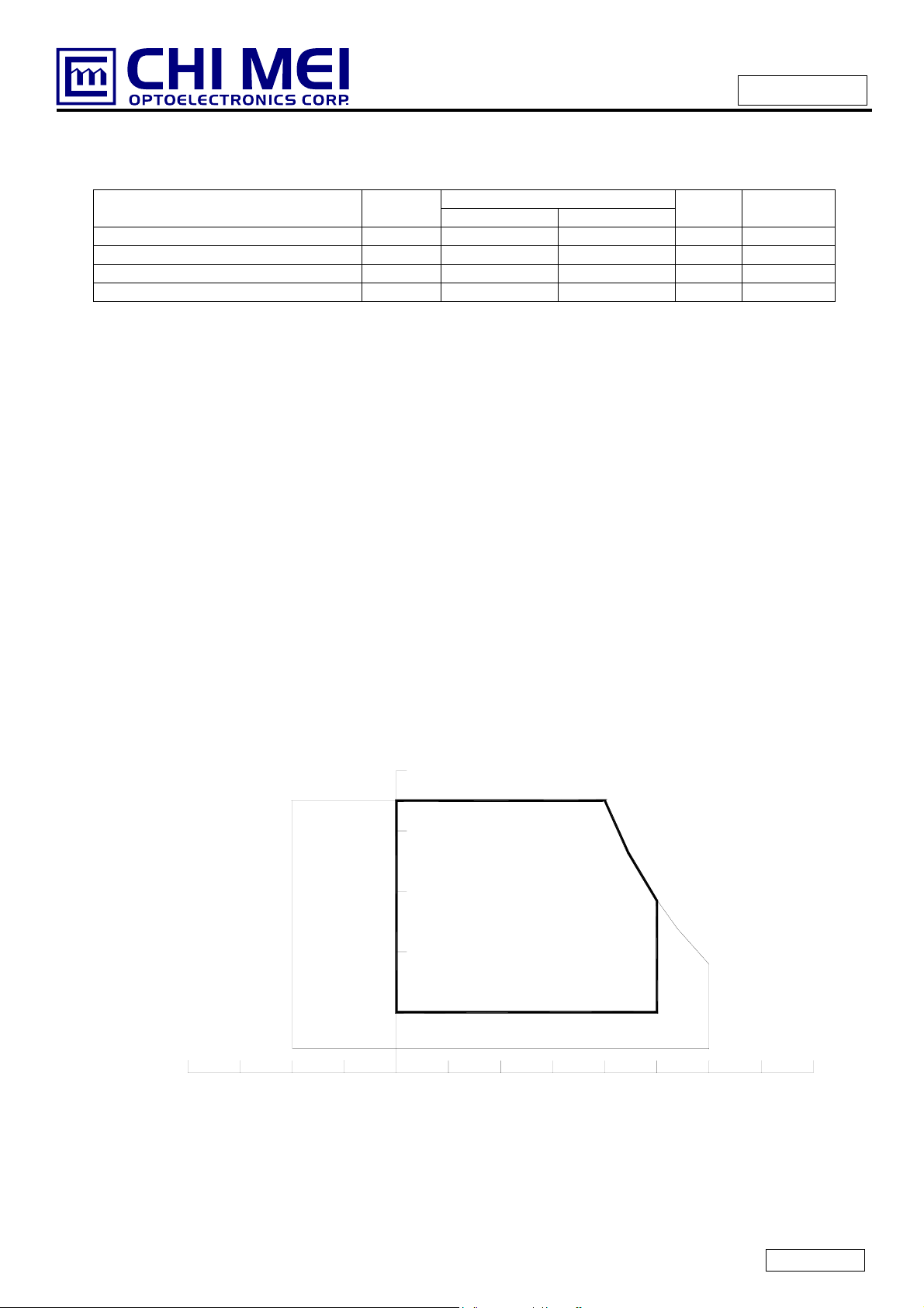
2. ABSOLUTE MAXIMUM RATINGS
2.1 ABSOLUTE RATINGS OF ENVIRONMENT
Item Symbol
Storage Temperature TST -20 +60 ºC (1)
Operating Ambient T emperature TOP 0 +50 ºC (1), (2)
Shock (Non-Operating) S
Vibration (Non-Operating) V
Note (1) Temperature and relative humidity range is shown in the figure below.
(a) 90 %RH Max. (Ta ≦ 40 ºC).
(b) Wet-bulb temperature should be 39 ºC Max. (Ta > 40 ºC).
(c) No condensation.
Note (2) The maximum operating temperature is based on the test condition that the surface temperature of
display area is less than or equal to 60 ºC with LCD module alone in a temperature controlled chamber.
Thermal management should be considered in final product design to prevent the surface temperature of
- 50 G (3), (5)
NOP
- 1.0 G (4), (5)
NOP
Min. Max.
Value
Unit Note
display area from being over 60 ºC. The range of operating temperature may degrade in case of
improper thermal management in final product design.
Note (3) 11 ms, half sine wave, 1 time for ± X, ± Y, ± Z.
Note (4) 10 ~ 200 Hz, 10 min, 1 time each X, Y, Z.
Note (5) At testing Vibration and Shock, the fixture in holding the module has to be hard and rigid enough so
that the module would not be twisted or bent by the fixture.
Relative Humidity (%RH)
100
90
80
60
Operating Range
40
-40 -20 0 20 40 60 80
20
10
Storage Range
Temperature (ºC)
2.2 ELECTRICAL ABSOLUTE RATINGS
5 / 34
The information described in this technical specification is tent ative and it is possible to be changed witho ut prior notice.
Please contact CMO ’s represent ative while your product design is based on this specification. Version 0.2
Page 6
Issued Date: 8/11/2004
Model No.: V370H1 – L01
Preliminary
2.2 ELECTRICAL ABSOLUTE RATINGS
2.2.1 TFT LCD MODULE
Item Symbol
Power Supply V oltage Vcc -0.3 20 V
Input Signal Volt age VIN -0.3 (3.6) V
2.2.2 BACKLIGHT INVERTER UNIT
Item Symbol
Lamp Voltage VW
Power Supply V oltage VBL 0 (150) V
Auxiliary Power Supply Voltage
Control Signal Level
Note (1) Permanent damage to the device may occur if maximum values are exceeded. Function operation
should be restricted to the conditions described under Normal Operating Conditions.
0 23 V (1)
V
AUX
-
Value
Min. Max.
Value
Min. Max.
-
3000 V
Unit Note
Unit Note
-0.3 7 V
RMS
(1), (3)
(1)
(1)
Note (2) No moisture condensation or freezing.
Note (3) The control signals includes On/Off Control, Internal PWM Control, External PWM Control and
Internal/External PWM Selection.
6 / 34
The information described in this technical specification is tent ative and it is possible to be changed witho ut prior notice.
Please contact CMO ’s represent ative while your product design is based on this specification. Version 0.2
Page 7
Issued Date: 8/11/2004
Model No.: V370H1 – L01
Preliminary
3. ELECTRICAL CHARACTERISTICS
3.1 TFT LCD MODULE Ta = 25 ± 2 ºC
Parameter Symbol
Min. Typ. Max.
Power Supply V oltage VCC 16.2 18 19.8 V (1)
Power Supply Ripple V oltage VRP - - 200 mV
Rush Current I
- 2 - A (2)
RUSH
White - 0.76 - A
Power Supply Current
Differential Input High
Threshold Voltage
LVDS
Interface
Differential Input Low
Threshold Voltage
Common Input V oltage V
Terminating Resistor R
Black - 0.41 - A
Vertical Stripe
ICC
- 0.59 - A
V
- - +100 mV
LVTH
V
-100 - - mV
LVTL
1.125 1.25 1.375 V
LVC
- 100 - ohm
T
Input High Threshold Voltage VIH 2.7 - 3.3 V CMOS
interface
Input Low Threshold Voltage VIL 0 - 0.7 V
Note (1) The module should be always operated within above ranges.
Value
Unit Note
(3)
Note (2) Measurement Conditions:
(High to Low)
(Control Signal)
SW
+12V
C1
1uF
+18
47K
R1
R2
1K
47K
2SK1475Q1
Q2
2SK1470
C2
0.01uF
Vcc rising time is 470µs
+18V
FUSE
C3
1uF
Vcc
(LCD Module Input)
0.9Vcc
0.1Vcc
GND
470µs
7 / 34
The information described in this technical specification is tent ative and it is possible to be changed witho ut prior notice.
Please contact CMO ’s represent ative while your product design is based on this specification. Version 0.2
Page 8
Issued Date: 8/11/2004
Model No.: V370H1 – L01
Preliminary
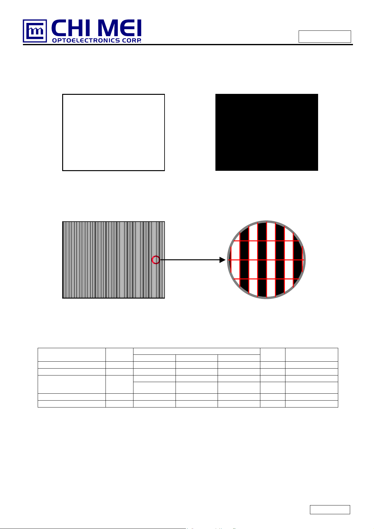
Note (3) The specified power supply current is under the conditions at Vcc = 18 V, Ta = 25 ± 2 ºC, fv = 60 Hz,
whereas a power dissipation check pattern below is displayed.
a. White Pattern
Active Area
c. Vertical Stripe Pattern
b. Black Pattern
Active Area
R
G
G
B
R
G
B
R
G
B
B
B
B
R
R
R
R R
G
G
G
G
B
B
B
B
R
R
Active Area
3.2 BACKLIGHT UNIT
3.2.1 CCFL (Cold Cathode Fluorescent Lamp) CHARACTERISTICS (
Parameter Symbol
Lamp Input Voltage VL --- 1300 --- V
Lamp Current IL 4.3 4.8 5.3 mA
Lamp Turn On Voltage VS
Operating Frequency FL 40 -- 70 KHz (3)
Lamp Life Time LBL 50K - - Hrs (5)
Min. Typ. Max.
- - 2440 V
-
Value
-
2780 V
Ta = 25 ± 2 ºC)
Unit Note
I
RMS
RMS
(2), Ta = 25 ºC
RMS
(2), Ta = 0 ºC
RMS
= (4.8) mA
L
(1)
8 / 34
The information described in this technical specification is tent ative and it is possible to be changed witho ut prior notice.
Please contact CMO ’s represent ative while your product design is based on this specification. Version 0.2
Page 9
Issued Date: 8/11/2004
)
)
(
)
)
(
)
(
)
)
(
)
(
)
AAAAA
AAAAAAAAAAAAAAA
Model No.: V370H1 – L01
Preliminary
3.2.2 INVERTER CHARACTERISTICS (Ta = 25 ± 2 ºC)
Parameter Symbol
Power consumption PBL - 150 - W (5), IL = 4.8mA
Power Supply V oltage VBL 108 120 132 VDC
Power Supply Current IBL - 1.4 - A Non Dimming
Auxiliary Power Supply Voltage
Auxiliary Power Supply Current I
Input Ripple Noise - - - 2.5 V
Backlight Turn on Voltage VBS
Oscillating Frequency FW 51 54 57 kHz
Dimming frequency FB 150 160 170 Hz
Minimum Duty Ratio D
Note (1) Lamp current is measured by utilizing high frequency current meters as shown below:
V
16 18 20 VDC
AUX
AUX
- 20 - %
MIN
Min. Typ. Max.
- - 1000 mA
2750
2410 - - V
Value
- -
Unit Note
VBL=108V
P-P
V
Ta = 0 ºC
RMS
Ta = 25 ºC
RMS
LCD
Module
HV (Pink,+)
HV (White,+
HV (Pink,-
HV (White,-)
HV (Pink,+)
HV (White,+)
Pink,-
HV
HV (White,-
HV (Pink,+)
HV
White,+
HV (Pink,-)
HV (White,-)
HV (Pink,+)
HV (White,+)
Pink,-
HV
HV (White,-
HV (Pink,+)
White,+
HV
1
2
1
2
1
2
1
2
1
2
1
2
1
2
1
2
1
2
Inverter
9 / 34
The information described in this technical specification is tent ative and it is possible to be changed witho ut prior notice.
Please contact CMO ’s represent ative while your product design is based on this specification. Version 0.2
HV (Pink,-)
White,-
HV
1
2
Return Cable
Page 10
Issued Date: 8/11/2004
yp
y
y
Model No.: V370H1 – L01
Preliminary
Note (2) The lamp starting voltage VS should be applied to the lamp for more than 1 second after startup.
Otherwise the lamp may not be turned on.
Note (3) The lamp frequency may produce interference with horizontal synchronous frequen cy of the display
input signals, and it may result in line flow on the display. In order to avoid interference, the lamp
frequency should be detached from the horizontal synchronous frequency and its harmonics as far
as possible.
Note (4) The life time of a lamp is defined as when the brightness is larger than 50% of its original value and
the effective discharge length is longer than 80% of its original length (Effective discharge length is
defined as an area that has equal to or more than 70% brightness comp ared to the bri ghtness at the
center point of lamp.) as the time in which it continues to operate under the condition at Ta = 25 ±2
℃ and I
= 4.3 ~ 5.3 mArms.
L
Note (5) The power supply capacity should be higher than the total inverter power consumption P
the pulse width modulation (PWM) mode was applied for backlight dimming, the driving current
changed as PWM duty on and off. The transient respo nse of power supply sho uld be consi dered for
the changing loading when inverter dimming.
3.2.3 INVERTER INTERTFACE CHARACTERISTICS
Parameter Symbol
Inverter Good Signal
On/Off Control Voltage
Select Volt age
Voltage
Voltage
HI V
LO
ON
OFF
HI
LO
MAX
MIN
HI 2.0
LO
V
V
V
V
VIG
BLON
SEL
IPWM
EPWM
Control Signal Rising Time Tr
Control Signal Falling Time Tf
PWM Signal Rising T ime T
PWM Signal Falling Tim e T
PWMR
PWMF
Input impedance RIN
BLON Delay Time1 T
BLON Off Time1 T
BLON Delay Time2 T
BLON Off Time2 T
on1
off1
on2
off2
- 500 - - ms
- 500 - - ms
- 500 - - ms
- 500 - - ms
Test
Condition
=High 2.0
=Low 0
V
-
-
-
-
V
SEL
V
SEL
- - -
- - -
- - -
- - -
-
Min. T
2.0
2.0
= L
= H
Note (1) The SEL signal should be valid before backlight turns on by BLON signal. It is inhibited to change
Value
-
-
-
0
-
-
0
-
-
- -
-
0
1
-
- - MΩ
.Max.
5.0 V normal Output
0.8 V abnormal Output
5.0 V
0.8 V
5.0 V Internal/External PWM
0.8 V
0
-
3.0 V maximum dut
5.0 V duty on External PWM Control
0.8 V dut
100 ms
100 ms
50 us
50 us
Unit Note
V minimum dutyratioInternal PWM Control
off
. Since
BL
ratio
the internal/external PWM selection (SEL) during backlight turn on period.
Note (2) The power sequence and control signal timing are shown in the following figure.
10 / 34
The information described in this technical specification is tent ative and it is possible to be changed witho ut prior notice.
Please contact CMO ’s represent ative while your product design is based on this specification. Version 0.2
Page 11
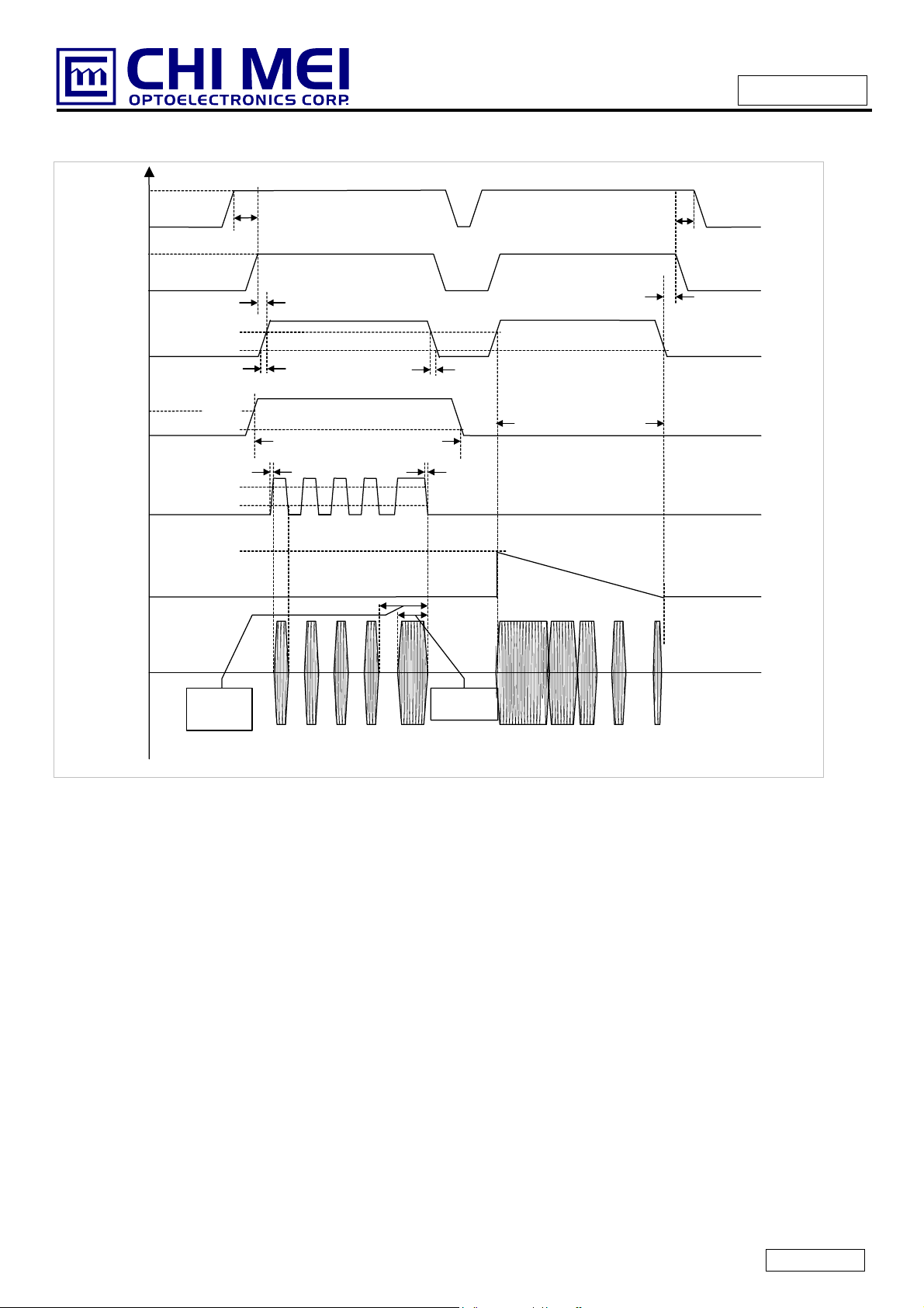
Issued Date: 8/11/2004
Model No.: V370H1 – L01
Preliminary
V
BL
V
V
V
V
CC
BLON
V
SEL
EPWM
IPWM
V
0
0
0
0
0
0
W
2.0V
0.8V
2.0V
0.8V
2.0V
0.8V
3.0V
External
PWM
Period
on1
T
T
on2
Backlight on duration
r
T
Ext. Dimming Function
T
PWMR
T
PWMF
T
f
External
PWM Duty
Int. Dimming Function
100%
T
Minimun
Duty
off2
T
off1
11 / 34
The information described in this technical specification is tent ative and it is possible to be changed witho ut prior notice.
Please contact CMO ’s represent ative while your product design is based on this specification. Version 0.2
Page 12

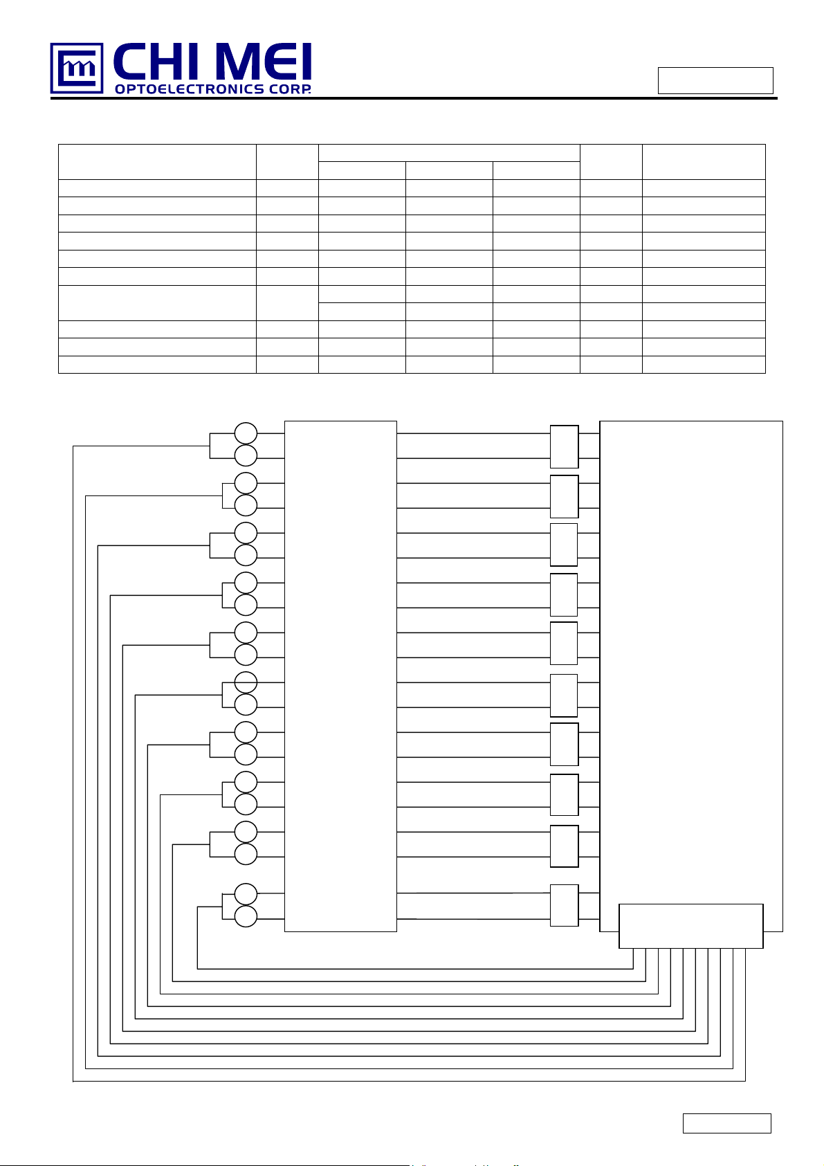
4. BLOCK DIAGRAM
)
V
4.1 TFT LCD MODULE
Issued Date: 8/11/2004
Model No.: V370H1 – L01
Preliminary
ERX0(+/-)
ERX1(+/-)
ERX2(+/-)
ERX3(+/-)
ERXC(+/-)
ORX0(+/-)
ORX1(+/-)
ORX2(+/-)
ORX3(+/-)
ORXC(+/-)
RPF
ODSEL1
ODSEL2
GND
VBL
GND
V
GND
IG
SYN
SEL
E_PWM
I_PWM
BLON
CN1
CN2
FRAME
(FI-X30SSL-HF (JAE))
INPUT CONNECTOR
BUFFER
TIMING
CONTROLLER
DC/DC CONVERTER
POWER
CONNECTOR
(53261-1519
(Molex))
INVERTER CONNECTOR
CN1:S12B-PH-SM3-TB(JST)
CN2: S10B-PH-SM3-TB(JST)
CN13: 53261-1019 (MOLEX)
& REFERENCE
VOLTAGE
GENERATOR
CN3-CN12:SM02 (8.0)B-BHS-1-TB
SCAN DRI
TFT LCD PANEL
(1920x3x1080)
ER
DA TA DRIVER (RSDS
BACKLIGHT UNIT
12 / 34
The information described in this technical specification is tent ative and it is possible to be changed witho ut prior notice.
Please contact CMO ’s represent ative while your product design is based on this specification. Version 0.2
Page 13

5. INTERFACE PIN CONNECTION
(3)
p
y
p
y
p
y
p
y
p
y
5.1 TFT LCD MODULE
CNF1 Connector Pin Assignment
Pin No. Symbol Description Note
1 GND Ground
2 RPF Display Rotation
3 NC No Connection
4 NC No Connection
5 NC No Connection
6 ODSEL1 Overdrive Lookup Table Selection
7 ODSEL2 Overdrive Lookup Table Selection
8 GND Ground
9 ERX0- Negative transmission data of Even pixel 0
10 ERX0+ Positive transmission data of Even pixel 0
11 ERX1- Negative transmission data of Even pixel 1
12 ERX1+ Positive transmission data of Even pixel 1
13 ERX2- Negative transmission data of Even pixel 2
14 ERX2+ Positive transmission data of Even pixel 2
15 ECLK- Negative of Even clock
16 ECLK+ Positive of Even clock
17 ERX3- Negative transmission data of Even pixel 3
18 ERX3+ Positive transmission data of Even pixel 3
19 GND Ground
20 ORX0- Negative transmission data of Odd pixel 0
21 ORX0+ Positive transmission data of Odd pixel 0
22 ORX1- Negative transmission data of Odd pixel 1
23 ORX1+ Positive transmission data of Odd pixel 1
24 ORX2- Negative transmission data of Odd pixel 2
25 ORX2+ Positive transmission data of Odd pixel 2
26 OCLK- Negative of Odd clock
27 OCLK+ Positive of Odd clock
28 ORX3- Negative transmission data of Odd pixel 3
29 ORX3+ Positive transmission data of Odd pixel 3
30 GND Ground
Issued Date: 8/11/2004
Model No.: V370H1 – L01
Preliminary
(4)
(5)
CNF2
The information described in this technical specification is tent ative and it is possible to be changed witho ut prior notice.
Please contact CMO ’s represent ative while your product design is based on this specification. Version 0.2
Connector Pin Assignment
Pin No. Symbol Description Note
1 VCC +18.0V
2 VCC +18.0V
3 VCC +18.0V
4 VCC +18.0V
5 VCC +18.0V
6 GND Ground
7 GND Ground
8 GND Ground
9 GND Ground
10 GND Ground
11 NC No Connection
12 NC No Connection
13 NC No Connection
14 NC No Connection
15 NC No Connection
ower suppl
ower suppl
ower suppl
ower suppl
ower suppl
(4)
13 / 34
Page 14

Issued Date: 8/11/2004
Model No.: V370H1 – L01
Preliminary
Note (1) CNF1 Connector part no.: FI-X30SSL-HF (JAE) or equivalent.
Note (2) CNF2 Connector part no.: 53261-1519 (Molex) or equivalent.
Note (3) Low : normal display (default), High : display with 180 degree rot ation
Note (4) Reserved for internal use. Left it open.
Note (5) Overdrive lookup table selection. The overdrive lookup table should be selected in accordance to the
frame rate to optimize image quality.
ODSEL2 ODSEL1 Note
L L Lookup table was optimized for 60 Hz frame rate.
L H Lookup table was optimized for 50 Hz frame rate.
H L Reserved. Do not use.
H H Reserved. Do not use.
14 / 34
The information described in this technical specification is tent ative and it is possible to be changed witho ut prior notice.
Please contact CMO ’s represent ative while your product design is based on this specification. Version 0.2
Page 15

Issued Date: 8/11/2004
Model No.: V370H1 – L01
Preliminary
5.2 BACKLIGHT UNIT
The pin configuration for the housing and leader wire is shown in the table below.
CN3-CN12: BHR-04VS-1 (JST).
Pin No. Symbol Description Wire Color
1 HV High Voltage Pink
2 HV High Voltage White
Note (1) The backlight interface housing for high voltage side is a model BHR-04VS-1, manufactured by JST.
The mating header on inverter part number is SM02(12.0)B-BHS-1-TB.
CN13: 51021-1000 (MOLEX) or equivalent
Pin No. Symbol Description Wire Color
1 LV Low Voltage Black
2 LV Low Voltage Black
3 LV Low Voltage Black
4 LV Low Voltage Black
5 LV Low Voltage Black
6 LV Low Voltage Black
7 LV Low Voltage Black
8 LV Low Voltage Black
9 LV Low Voltage Black
10 LV Low Voltage Black
Note(2) The backlight interface housing and return cable for low voltage side is a model 51021-1000,
manufactured by MOLEX or equivalent. The mating header on inverter part num ber is 53261-1019
(MOLEX) or equivalent.
1 HV(Pink,+)
2 HV(White,+)
1 HV(Pink,-)
2 HV(White,-)
1 HV(Pink,+)
2 HV(White,+)
1 HV(Pink,-)
2 HV(White,-)
RETURN CABLE
LV (Black,+)
LV (Black,-)
LV (Black,+)
LV (Black,-)
15 / 34
The information described in this technical specification is tent ative and it is possible to be changed witho ut prior notice.
Please contact CMO ’s represent ative while your product design is based on this specification. Version 0.2
Page 16

5.3 INVERTER UNIT
CN1(Header):S12B-PH-SM3-TB (JST) or equivalent.
Pin No. Symbol Description
1
2
VBL +120V
3
4
5
NC NC
6
7
8
GND GND
9
10
11
12
Vcc 18V
CN2(Header): S10B-PH-SM3-TB (JST) or equivalent.
Pin No. Symbol Description
1
2
GND GND
3
4 NC NC
5 IG Inverter Good Signal
6 SYN Synchronous control
Internal/external PWM selection
7
SEL
High : external dimming
Low : internal dimming
External PWM control signal
8 E_PWM
E_PWM should be connected to ground when internal PWM was se lected (SEL =
low).
Internal PWM control signal
9
I_PWM
I_PWM should be connected to ground when external PWM was selected (SEL =
high).
10
BLON Backlight on/off control
CN3-CN12(Header): SM02(12)B-BHS-1-TB (JST)
Pin No. Symbol Description
1
2
CCFL HOT
CCFL HOT
CCFL high voltage
CCFL high voltage
CN13(Header): 53261-1019 (Molex) or equivalent
Pin No. Symbol Description
1
2
3
4
5
6
7
8
9
10
CCFL Cold
CCFL Cold
CCFL Cold CFL Low voltage
CCFL Cold CFL Low voltage
CCFL Cold CFL Low voltage
CCFL Cold CFL Low voltage
CCFL Cold CFL Low voltage
CCFL Cold CFL Low voltage
CCFL Cold CFL Low voltage
CCFL Cold
CFL Low voltage
CFL Low voltage
CFL Low voltage
Note (1) Floating of any control signal is not allowed.
Power input
DC
DC
Issued Date: 8/11/2004
Model No.: V370H1 – L01
Preliminary
16 / 34
The information described in this technical specification is tent ative and it is possible to be changed witho ut prior notice.
Please contact CMO ’s represent ative while your product design is based on this specification. Version 0.2
Page 17

5.4 BLOCK DIAGRAM OF INTERFACE
C
OB0
OG0
G0-EG
0
r
0
OB0
OG0
p
O
ORx0
0
G0-EG
CNF1
Issued Date: 8/11/2004
Model No.: V370H1 – L01
Preliminary
ERx0+
ER0-ER7
E
EB
7
-EB7
DE
OR0-OR7
-OG7
-OB7
LK
D
TxIN
PLL
ERx
ERx1+
ERx1-
ERx2+
ERx2-
ERx3+
ERx3-
ECLK+
Host
Graphics
Controller
ORx0+
ORx1+
ORx1-
51Ω
-
100pF
51Ω
51Ω
100pF
51Ω
51Ω
100pF
51Ω
51Ω
100pF
51Ω
RxOUT
ER0-ER7
E
EB
-EB7
DE
OR0-OR7
-OG7
7
-OB7
51Ω
-
100pF
51Ω
PLL
DCLK
Timing
51Ω
51Ω
51Ω
100pF
100
F
-
Controlle
ORx2+
Rx2-
ORx3+
ORx3-
51Ω
100pF
51Ω
51Ω
100pF
51Ω
PLL
OCLK+
51Ω
-
100pF
51Ω
PLL
L V DS Transmitter
THC63LVDM83A
(LVDF83A)
LVDS Receiver
17 / 34
The information described in this technical specification is tent ative and it is possible to be changed witho ut prior notice.
Please contact CMO ’s represent ative while your product design is based on this specification. Version 0.2
Page 18

ER0~ER7 : Even pixel R data
EG0~EG7 : Even pixel G data
EB0~EB7 : Even pixel B data
OR0~OR7 : Odd pixel R data
OG0~OG7: Odd pixel G data
OB0~OB7 : Odd pixel B data
DE : Data ena ble signal
DCLK : Data clock signal
Notes: (1) The syste m must have the transmitter to drive the module.
(2) LVDS cable impedance shall be 50 ohms per signal line or about 100 ohms per twist-pair line when it is
used differentially.
(3) Two pixel data send into the module for every cloc k cy cle. The first pixel of the frame is even pixel and
Issued Date: 8/11/2004
Model No.: V370H1 – L01
Preliminary
the second pixel is odd pixel.
18 / 34
The information described in this technical specification is tent ative and it is possible to be changed witho ut prior notice.
Please contact CMO ’s represent ative while your product design is based on this specification. Version 0.2
Page 19

5.5 LVDS INTERFACE
SIGNAL
TRANSMITTER
THC63LVDM83A
PIN INPUT Host TFT-LCD PIN OUTPUT
INTERFACE CONNECTOR
RECEIVER
THC63LVDF84A
Issued Date: 8/11/2004
Model No.: V370H1 – L01
Preliminary
TFT CONTROL
INPUT
24bit
R0
R1
R2
R3
R4
R5
G0
G1
G2
G3
G4
G5
B0
B1
B2
B3
B4
B5
DE
R6
R7
G6
G7
B6
B7
RSVD 1
RSVD 2
RSVD 3
DCLK 31 TxCLK IN TxCLK OUT+
51
52
54
55
56
3
4
6
7
11
12
14
15
19
20
22
23
24
30
50
2
8
10
16
18
25
27
28
TxIN0
TxIN1
TxIN2
TxIN3
TxIN4
TxIN6
TxIN7
TxIN8
TxIN9
TxIN12
TxIN13
TxIN14
TxIN15
TxIN18
TxIN19
TxIN20
TxIN21
TxIN22
TxIN26
TxIN27
TxIN5
TxIN10
TxIN11
TxIN16
TxIN17
TxIN23
TxIN24
TxIN25
TA OUT0+
TA OUT0-
TA OUT1+
TA OUT1-
TA OUT2+
TA OUT2-
TA OUT3+
TA OUT3-
TxCLK OUT-
Rx 0+
Rx 0-
Rx 1+
Rx 1-
Rx 2+
Rx 2-
Rx 3+
Rx 3-
RxCLK IN+
RxCLK IN-
27
29
30
32
33
35
37
38
39
43
45
46
47
51
53
54
55
1
6
7
34
41
42
49
50
2
3
5
26 RxCLK OUT DCLK
Rx OUT0
Rx OUT1
Rx OUT2
Rx OUT3
Rx OUT4
Rx OUT6
Rx OUT7
Rx OUT8
Rx OUT9
Rx OUT12
Rx OUT13
Rx OUT14
Rx OUT15
Rx OUT18
Rx OUT19
Rx OUT20
Rx OUT21
Rx OUT22
Rx OUT26
Rx OUT27
Rx OUT5
Rx OUT10
Rx OUT11
Rx OUT16
Rx OUT17
Rx OUT23
Rx OUT24
Rx OUT25
R0
R1
R2
R3
R4
R5
G0
G1
G2
G3
G4
G5
B0
B1
B2
B3
B4
B5
DE
R6
R7
G6
G7
B6
B7
Not connect
Not connect
Not connect
R0~R7: Pixel R Data (7; MSB, 0; LSB)
G0~G7: Pixel G Data (7; MSB, 0; LSB)
B0~B7: Pixel B Data (7; MSB, 0; LSB)
DE : Data enable signal
DCLK : Data clock signal
Notes: (1) RSVD(reserved)pins on the transmitter shall be “H” or “L”.
19 / 34
The information described in this technical specification is tent ative and it is possible to be changed witho ut prior notice.
Please contact CMO ’s represent ative while your product design is based on this specification. Version 0.2
Page 20

Issued Date: 8/11/2004
Model No.: V370H1 – L01
Preliminary
5.6 COLOR DATA INPUT ASSIGNMENT
The brightness of each primary color (red, green and blue) is based on the 8-bit gray scale data input for
the color. The higher the binary input, the brig hter the color. The table below provides the assignment of color
versus data input.
Data Signal
Basic
Colors
Gray
Scale
Of
Red
Color
Black
Red
Green
Blue
Cyan
Magenta
Yellow
White
Red(0) / Dark
Red(1)
Red(2)
:
:
Red(253)
Red(254)
Red(255)
R7 R6 R5 R4 R3 R2 R1 R0 G7 G6 G5 G4 G3 G2 G1 G0 B7 B6 B5 B4 B3 B2 B1 B0
0
0
1
1
0
0
0
0
0
0
1
1
1
1
1
1
0
0
0
0
0
0
:
:
:
:
1
1
1
1
1
1
Red Green Blue
0
0
0
0
0
0
0
0
0
0
0
0
0
0
0
0
0
0
0
1
1
1
1
1
1
0
0
0
0
0
0
0
0
0
0
0
0
0
0
0
0
0
0
0
1
1
1
1
1
1
1
1
0
0
0
0
0
0
0
0
0
0
0
0
0
0
0
0
0
0
0
1
1
1
1
1
0
0
0
0
0
0
1
1
1
1
1
1
1
1
1
1
1
1
1
1
1
1
1
1
1
0
0
0
0
0
0
0
0
1
1
1
1
1
1
1
1
1
1
1
1
1
1
1
1
1
1
1
0
0
0
0
0
1
1
1
1
1
1
1
1
1
1
1
1
1
1
1
1
1
1
1
0
0
0
0
0
0
0
0
0
0
0
0
0
0
0
0
0
0
0
0
0
0
0
0
1
0
0
0
0
0
0
0
0
0
0
0
0
0
0
0
0
0
1
0
0
0
0
0
0
0
0
0
0
0
0
0
0
:
:
:
:
:
:
:
:
:
:
:
:
:
:
:
:
:
:
:
:
:
:
:
:
:
:
:
:
:
:
:
:
:
:
:
:
:
:
1
1
1
1
0
1
0
0
0
0
0
0
0
0
0
0
0
0
0
1
1
1
1
1
0
0
0
0
0
0
0
0
0
0
0
0
0
0
1
1
1
1
1
1
0
0
0
0
0
0
0
0
0
0
0
0
0
0
0
0
0
0
0
0
0
0
1
1
1
1
1
1
1
1
1
0
0
0
1
1
1
0
0
0
0
0
0
0
0
0
:
:
:
:
:
:
0
0
0
0
0
0
0
0
0
Gray
Scale
Of
Green
Gray
Scale
Of
Blue
Green(0) / Dark
Green(1)
Green(2)
:
:
Green(253)
Green(254)
Green(255)
Blue(0) / Dark
Blue(1)
Blue(2)
:
:
Blue(253)
Blue(254)
Blue(255)
0
0
0
0
0
0
0
0
0
0
0
0
0
0
0
0
0
0
0
0
0
0
0
0
0
0
0
0
0
0
0
0
0
:
:
:
:
:
:
:
:
:
:
:
:
:
:
:
:
:
:
:
:
0
0
0
0
0
0
0
0
1
1
1
0
0
0
0
0
0
0
0
1
1
1
0
0
0
0
0
0
0
0
1
1
1
0
0
0
0
0
0
0
0
0
0
0
0
0
0
0
0
0
0
0
0
0
0
0
0
0
0
0
0
0
0
0
0
0
:
:
:
:
:
:
:
:
:
:
:
:
:
:
:
:
:
:
:
:
0
0
0
0
0
0
0
0
0
0
0
0
0
0
0
0
0
0
0
0
0
0
0
0
0
0
0
0
0
0
0
0
0
Note (1) 0: Low Level Voltage, 1: High Level Voltage
0
0
0
0
0
0
0
0
0
0
0
0
0
0
0
0
0
1
0
0
0
0
0
0
0
0
0
0
0
1
0
0
0
0
0
0
0
0
0
:
:
:
:
:
:
:
:
:
:
:
:
:
:
:
:
:
:
:
:
:
:
:
:
:
:
:
:
1
1
1
0
1
0
0
0
0
0
0
0
0
1
1
1
1
0
0
0
0
0
0
0
0
0
1
1
1
1
1
0
0
0
0
0
0
0
0
0
0
0
0
0
0
0
0
0
0
0
0
0
0
0
0
0
0
0
0
0
0
0
0
0
1
0
0
0
0
0
0
0
0
0
0
0
1
0
:
:
:
:
:
:
:
:
:
:
:
:
:
:
:
:
:
:
:
:
:
:
:
:
:
:
:
:
0
0
0
0
0
1
1
1
1
1
1
0
1
0
0
0
0
0
1
1
1
1
1
1
1
0
0
0
0
0
0
1
1
1
1
1
1
1
1
20 / 34
The information described in this technical specification is tent ative and it is possible to be changed witho ut prior notice.
Please contact CMO ’s represent ative while your product design is based on this specification. Version 0.2
Page 21

Issued Date: 8/11/2004
g
y
(60)74(80)
)
)
(
)
(
(35)45(55)
(
(
(
)
(
v
Model No.: V370H1 – L01
Preliminary
6. INTERFACE TIMING
6.1 INPUT SIGNAL TIMING SPECIFICATIONS
The input signal timing specifications are shown as the following table and timing diagram.
Si
nal Item Symbol Min. Typ. Max. Unit Note
LVDS Receiver Clock Frequenc
LVDS Receiver Data
Vertical Active Display T erm
Horizontal Active Display Term
Note (1) Since this module is operated in DE only mode, Hsync and Vsync input signal s shoul d be set to low
logic level. Otherwise, this module would operate abnormally.
Setup Time Tlvsu 600 - - ps
Hold Time Tlvhd 600 - - ps
Frame Rate
Total Tv
Display Tvd 1080 1080 1080 Th Blank Tvb
Total Th
Display Thd 1920 1920 1920 Tc Blank Thb
1/Tc
Fr5 47 50 53 Hz (2
Fr6 57 60 63 Hz (3
1115
2100)2200
180
1125
280
MHZ
1135) Th Tv=Tvd+Tvb
Th -
2300) Tc Th=Thd+Thb
380) Tc -
(2) (ODSEL2, ODSEL1) = (L,H). Please refer to 5.1 for detail information.
(3) (ODSEL2, ODSEL1) = (L,L). Please refer to 5.1 for detail information.
INPUT SIGNAL TIMING DIAGRAM
DE
Th
DCLK
Tc
DE
Tvd
Thb
T
Thd
Tvb
The information described in this technical specification is tent ative and it is possible to be changed witho ut prior notice.
Please contact CMO ’s represent ative while your product design is based on this specification. Version 0.2
DATA
Valid display data (960 clocks)
21 / 34
Page 22

Issued Date: 8/11/2004
Model No.: V370H1 – L01
Preliminary
LVDS RECEIVER INTERFACE TIMING DIAGRAM
RXCLK+/-
RXn+/-
Tlvsu
Tlvhd
1T
14
3T
14
5T
14
Tc
7T
14
9T
14
11T
14
13T
14
22 / 34
The information described in this technical specification is tent ative and it is possible to be changed witho ut prior notice.
Please contact CMO ’s represent ative while your product design is based on this specification. Version 0.2
Page 23

Issued Date: 8/11/2004
Model No.: V370H1 – L01
Preliminary
6.2 POWER ON/OFF SEQUENCE
To prevent a latch-up or DC operation of LCD module, the power on/off sequence should be as the diagram
below.
Power Supply
V
0≦T1≦10ms
2≦50ms
0≦T
3≦50ms
0≦T
500ms≦T
CC
0V
4
Signals
0V
Backlight (Recommended)
500ms≦T
100ms≦T6
5
0.9 VCC
CC
0.1V
Power On
T1
CC
0.9 V
CC
0.1V
3
T
T
2
T4
VALID
Power Off
50%
T5
50%
6
T
Power ON/OFF
Note.
(1) The supply voltage of the external system for the module input should follow the definition of Vcc.
(2) Apply the lamp voltage within the LCD operation ran ge. When the backlig ht turns on before the LCD operation
or the LCD turns off before the backlight turns off, the displ ay may momentarily become abnormal screen.
(3) In case of VCC is in off level, please keep the level of input signals on the low or high impedance.
(4) T4 should be measured after the module ha s been fully discharged between power off and on period.
(5) Interface signal shall not be kept at high impedance when the power is on.
23 / 34
The information described in this technical specification is tent ative and it is possible to be changed witho ut prior notice.
Please contact CMO ’s represent ative while your product design is based on this specification. Version 0.2
Page 24

Issued Date: 8/11/2004
)
)
)
(5)
y
(
(
y
(72)
(75)
Model No.: V370H1 – L01
Preliminary
7. OPTICAL CHARACTERISTICS
7.1 TEST CONDITIONS
Item Symbol Value Unit
Ambient Temperature T a
Ambient Humidity Ha
25±2
50±10
Supply Volt age VCC 5.0 V
Input Signal According to typical value in "3. ELECTRICAL CHARACTERISTICS"
Lamp Current IL
Oscillating Frequency (Inverter) FW
4.8±0.5
54±3
7.2 OPTICAL SPECIFICATIONS
The relative measurement methods of optical characteristics are shown in 7.2. The following items should
be measured under the test conditions described in 7.1 and stable environment shown in Note (6).
Item Symbol Condition Min. Typ. Max. Unit Note
Contrast Ratio CR TBD(700
Response time
Gray to gray
- (12) TBD ms (3)
average
Center Luminance of White L
Average Luminance of White L
White Variation
Cross Talk CT - - 4.0 %
Red
Green
C
TBD (500) - cd/m
AVE
θ
δW
Rx TBD
TBD
R
Gx TBD
=0°, θY =0°
x
Viewing Normal
Angle
Gy TBD
Bx TBD
Chromaticity
Blue
White
By TBD
Wx TBD 0.285 TBD -
TBD 0.293 TBD -
W
TBD (550) - cd/m
- - 1.3 - (7
(0.652)
(0.333)
(0.273)
0.598)
0.142)
(0.072)
Color Gamut CG
(80) (88) (80) (88) -
(80) (88) (80) (88) -
Viewing
Angle
Horizontal
Vertical
θ
+
x
θ
-
x
θ
+
Y
θ
-
Y
CR≥20
- - (2
TBD TBD TBD TBD -
TBD TBD -
- % NTSC
o
C
%RH
mA
KHz
2
(4)
2
(6) Color
Deg. (1)
24 / 34
The information described in this technical specification is tent ative and it is possible to be changed witho ut prior notice.
Please contact CMO ’s represent ative while your product design is based on this specification. Version 0.2
Page 25

Note (1) Definition of Viewing Angle (θx, θy):
Viewing angles are measured by EZ-Contrast 160R (Eldim)
Issued Date: 8/11/2004
Model No.: V370H1 – L01
Preliminary
θX- = 90º
x-
6 o’clock
θ
y- = 90º
y-
Note (2) Definition of Contrast Ratio (CR):
The contrast ratio can be calculated by the following expression.
Contrast Ratio (CR) = L255 / L0
L255: Luminance of gray level 255
Normal
θx = θy = 0º
θy+ θy-
θx−
θx+
y+
12 o’clock direction
θ
y+ = 90º
x+
θX+ = 90º
L 0: Luminance of gray level 0
CR = CR (5)
CR (X) is corresponding to the Contrast Ratio of the point X at the figure in Note (7).
Note (3) Definition of Gray to Gray Switching Time:
100%
90%
Optical
Response
10%
0%
Gray to gray
switching time
The driving signal means the signal of gray level 0, 63, 127, 191, 255.
Time
Time
Gray to gray
switching time
Gray to gray average time means the average switching time of gray level 0 ,63,127,191,255 to each
other.
25 / 34
The information described in this technical specification is tent ative and it is possible to be changed witho ut prior notice.
Please contact CMO ’s represent ative while your product design is based on this specification. Version 0.2
Page 26

Issued Date: 8/11/2004
A
A
Model No.: V370H1 – L01
Preliminary
Note (4) Definition of Luminance of White (LC, L
Measure the luminance of gray level 255 at center point and 5 points
LC = L (5)
L
= [L (1)+ L (2)+ L (3)+ L (4)+ L (5)] / 5
AVE
L (x) is corresponding to the luminance of the point X at the figure in Note (7).
Note (5) Definition of Cross Talk (CT):
CT = | Y
– YA | / YA × 100 (%)
B
Where:
= Luminance of measured location without gray level 0 pattern (cd/m2)
Y
A
YB = Luminance of measured location with gray level 0 pattern (cd/m2)
(0, 0)
ctive Area
Y
(D/8,W/2)
A, L
Y
(D/2,7W/8)
A, D
Gray 128
Y
A, U
Y
A, R
(D,W)
):
AVE
(D/2,W/8)
(7D/8,W/2)
(D/4,W/4)
Y
(D/8,W/2)
B, L
Y
(D/2,7W/8)
B, D
(0, 0)
ctive Area
Gray 0
Gray 0
Gray 128
Y
B, U
Y
B, R
(3D/4,3W/4)
(D,W)
(D/2,W/8)
(7D/8,W/2)
26 / 34
The information described in this technical specification is tent ative and it is possible to be changed witho ut prior notice.
Please contact CMO ’s represent ative while your product design is based on this specification. Version 0.2
Page 27

Issued Date: 8/11/2004
Model No.: V370H1 – L01
Preliminary
Note (6) Measurement Setup:
The LCD module should be stabilized at given temperature for 1 hour to avoid abrupt temperature
change during measuring. In order to stabilize the luminance, the measurement shoul d be executed
after lighting Backlight for 1 hour in a windless room.
LCD Module
Note (7) Definition of White Variation (δW):
Measure the luminance of gray level 255 at 5 points
δW = Maximum [L (1), L (2), L (3), L (4), L (5 )] / Minimum [L (1), L (2), L (3), L (4), L (5)]
LCD Panel
Center of the Screen
Display Color Analyzer
(Minolta CA210)
Light Shield Room
(Ambient Luminance < 2 lux)
Horizontal Line
D
3D/4D/2D/4
W
W/4
W/2
5
Vertical Line
3W/4
21
X
: Test Point
X=1 to 5
43
Active Area
27 / 34
The information described in this technical specification is tent ative and it is possible to be changed witho ut prior notice.
Please contact CMO ’s represent ative while your product design is based on this specification. Version 0.2
Page 28

Issued Date: 8/11/2004
Model No.: V370H1 – L01
Preliminary
8. DEFINITION OF LABELS
8.1 CMO MODULE LABEL
The barcode nameplate is pasted on each module as illustration, a nd its definitions are as following explanation.
CHI MEI
OPTOELECTRONICS
V370H1 -L01 Rev. XX
E207943
MADE IN TAIWAN
X X X X X X X Y M D L N N N N
(a) Model Name: V370H1-L01
(b) Revision: Rev. XX, for example: A0, A1… B1, B2… or C1, C2…etc.
(c) Serial ID: X X
Serial ID includes the information as below:
X X X X X Y M D L N N N N
Serial No.
Product Line
Year, Month, Date
CMO Internal Use
CMO Internal Use
Revision
CMO Internal Use
(a) Manufactured Date: Year: 0~9, for 2000~2009
Month: 1~9, A~C, for Jan. ~ Dec.
Day: 1~9, A~Y, for 1
(b) Revision Code: Cover all the change
(c) Serial No.: Manufacturing sequence of product
(d) Product Line: 1 -> Line1, 2 -> Line 2, …etc.
The information described in this technical specification is tent ative and it is possible to be changed witho ut prior notice.
Please contact CMO ’s represent ative while your product design is based on this specification. Version 0.2
st
to 31st, exclude I ,O, and U.
28 / 34
Page 29

9. PACKAGING
9.1 PACKING SPECIFICATIONS
(1) 3 LCD TV modules / 1 Box
(2) Box dimensions : 1048(L) X 345 (W) X 676 (H)
(3) Weight : approximately 33Kg ( 3 modules per box)
9.2 PACKING METHOD
Figures 9-1 and 9-2 are the packing method
LCD TV Module
Issued Date: 8/11/2004
Model No.: V370H1 – L01
Preliminary
CAUTION
HIGH VOLTAGE
DISCONNECT THE ELECTRIC
POWER BEFORE SERVICING.
RISK OF ELECTRIC SHOCK.
COLD CATHODE FLUORESCENT LAMP IN LCD PANEL CONTAINS A SMALL AMOUNT OF
MERCURY PLEASE FOLLOW LOCAL ORDINANCES OR REGULATIONS FOR DISPOSAL.
Anti-static Bag
PE Foam(Bottom)
Carton
CAUTION
HIGH VOLTAGE
DISCONNECT THE ELECTRIC
POWER BEFORE SERVICING.
RISK OF ELECTRIC SHOCK.
COLD CATHODE FLUORESCENT LAMP IN LCD PANEL CONTAINS A SMALL AMOUNT OF
MERCURY PLEASE FOLLOW LOCAL ORDINANCES OR REGULATIONS FOR DISPOSAL.
3pcs Drier
CAUTION
HIGH VOLTAGE
DISCONNECT THE ELECTRIC
POWER BEFORE SERVICING.
RISK OF ELECTRIC SHOCK.
COLD CATHODE FLUORESCENT LAMP IN LCD PANEL CONTAINS A SMALL AMOUNT OF
MERCURY PLEASE FOLLOW LOCAL ORDINANCES OR REGULATIONS FOR DISPOSAL.
Figure.9-1 packing method
Carton dimensions: 1048(L)x345(W)x676(H)mm
Weight
: Approx.33Kg(3 modules per 1 carton)
Carton Label
29 / 34
The information described in this technical specification is tent ative and it is possible to be changed witho ut prior notice.
Please contact CMO ’s represent ative while your product design is based on this specification. Version 0.2
Page 30

Film
Issued Date: 8/11/2004
Model No.: V370H1 – L01
Preliminary
Corner Protector:L1350*50mm*50mm
Pallet:L1100*W1100*H145mm
Bottom Cap:L1100*W1100*H120mm
Pallet Stack:L1100*W1100*H1500mm
Gross:218kg
PE Sheet
Bottom Cap
Carton Label
PP Belt
Figure. 9-2 Packing method
30 / 34
The information described in this technical specification is tent ative and it is possible to be changed witho ut prior notice.
Please contact CMO ’s represent ative while your product design is based on this specification. Version 0.2
Page 31

Issued Date: 8/11/2004
Model No.: V370H1 – L01
Preliminary
10. PRECAUTIONS
10.1 ASSEMBL Y AND HANDLING PRECAUTIONS
(1) Do not apply rough force such as bending or twisting to the module during assembly.
(2) It is recommended to assemble or to install a module into the user’s system in clean working areas. The
dust and oil may cause electrical short or worsen the polarizer.
(3) Do not apply pressure or impulse to the module to prevent the damage of LCD panel and backlight.
(4) Always follow the correct power-on sequence when the LCD module is turned on. This can prevent the
damage and latch-up of the CMOS LSI chips.
(5) Do not plug in or pull out the I/F connector while the module is in operation.
(6) Do not disassemble the module.
(7) Use a soft dry cloth without chemicals for cleaning, because the surface of polarizer is very soft and
easily scratched.
(8) Moisture can easily penetrate into LCD module and may cause the damage during operation.
(9) High temperature or humidity may deteriorate the performance of LCD module. Please store LCD
modules in the specified storage conditions.
(10) When ambient temperature is lower than 10ºC, the display quality might be reduced. For example, the
response time will become slow, and the starting voltage of CCFL will be higher than that of room
temperature.
10.2 SAFETY PRECAUTIONS
(1) The startup voltage of a backlight is over 1000 Volts. It may cause an electrical shock while assembling
with the inverter. Do not disassemble th e module or insert anything into the backlight unit.
(2) If the liquid crystal material leaks from the panel, it should be kept away from the eyes or mouth. In case
of contact with hands, skin or clothes, it has to be washed away thoroughly with soap.
(3) After the module’s end of life, it is not harmful in case of normal operation and storage.
31 / 34
The information described in this technical specification is tent ative and it is possible to be changed witho ut prior notice.
Please contact CMO ’s represent ative while your product design is based on this specification. Version 0.2
Page 32

11. MECHANICAL CHARACTERISTIC
Issued Date: 8/11/2004
Model No.: V370H1 – L01
Preliminary
奇美電子股份有限公司
CHI MEI
32 / 34
The information described in this technical specification is tent ative and it is possible to be changed witho ut prior notice.
Please contact CMO ’s represent ative while your product design is based on this specification. Version 0.2
Page 33

Issued Date: 8/11/2004
Model No.: V370H1 – L01
Preliminary
奇美電子股份有限公司
CHI MEI
COLD CATHODE FLUORESCENT LAMP IN LCD PANEL CONTAINS A SMALL AMOUNT OF
MERCURY PLEASE FOLLOW LOCAL ORDINANCES OR REGULATIONS FOR DISPOSAL.
POWER BEFORE SERVICING.
DISCONNECT THE ELECTRIC
RISK OF ELECTRIC SHOCK.
CAUTION
HIGH VOLTAGE
33 / 34
The information described in this technical specification is tent ative and it is possible to be changed witho ut prior notice.
Please contact CMO ’s represent ative while your product design is based on this specification. Version 0.2
Page 34

Issued Date: 8/11/2004
Model No.: V370H1 – L01
Preliminary
奇美電子股份有限公司
CHI MEI
34 / 34
The information described in this technical specification is tent ative and it is possible to be changed witho ut prior notice.
Please contact CMO ’s represent ative while your product design is based on this specification. Version 0.2
 Loading...