

Page 1
Global LCD Panel Exchange Center
x
ploy
g
Inbo
www.panelook.com
•••••••••••••••••••••••••••••• • •• •••••••••••• ••••••••••••••••••••••••••••••••••••••••
Display
Sender
Date
Subject
* The date is based on Korean standard time(GMT+9)
Created Date
Requested by
Subject
EDMS Attributes
••••••••••••••••••••••••••••••
2006/12/06 17:02
[Approval] LCD Module (V320B1 L04)
2006-12-01 22:27 (Korea Time)
• • • •••••
[Approval] LCD Module (V320B1 L04)
( Display
Biz Map
Team Map
Permission for
Other em
Doc Type
Info Type
Security Grade
••••••••••••••/••••••••••
Develop New Products and Services > Product Verification
••••••••••••••••••
Browse
ees
Approval
Reference
Internal use (Only)
(jimzzo@lge.com, 82-054-470-5232)
, 82-054-470-5232 )
> 2005
••••••••••••••••••••••••••••
Retention
Doc Language
>
••••••••••••••>••••
5 Year
Korean
New Development Component Information
ࣶ࣯ࣿࣜࣜ
ࣶ࣯࣮࣯ࣩࣜࣜࣿ
ࣶ࣭࣮࣯ࣜࣜࣜࣤࣥࣜࣤࣥࣜࣤࣥࣜࣜࣤᆬࣥ
ࣰࣶࣜࣜࣜࣤࣥࣜࣤࣥࣜࣜࣤࣥࣜࣤᆬࣥ
ࣶࣶࣜࣜࣜࣤࣥࣜࣜࣤࣜࣜࣥ
ࣶࣿࣜࣜࣜࣿࣜ
ࣶࣜࣜ
ࣶࣜࣜࣿ
ࣶ
CHI MEI OPTOELECTRONICS CORP
ࣶࣜࣜࣜࣿࣜࣜࣜࣜ儢愢
Key Parts : Source IC : Himax Gate IC : Himax T-con : Kawasaki Inverter : CMO Lamp : West, GIO
Application Model : 32LC3R-ZJ
Cut In Date : From Nov/E
EAJ33864501
V320B1-L04 WXGA 32.0INCH 1366X768 500CD COLOR 75% 16/9 1200 Response time : 6.5ms L01
•
Safety Standard Parts [
••
Power Cord, Power Plug, X / Y-Capacitor, Power Switch, Fuse, SMPS Trans, Stand-By Trans, Photo coupler,
Insulation (
Line Filter, PCB Material, Front / Back-cover Material, Relay(1-2
EMC Standard Parts [
••
Power Plug, Line Filter, X-Capacitor, Y-Capacitor, SMPS Trans, Tuner, Saw-Filter, Shield Case, Oscillator, Pattern Chan
Green [
••
This item must meet the standards of LG Electronics for six major substances as designated by RoHS for control.
) Resistor, Discharge (
••••
••••••••••••••••••
••••••••••••••
••••••••••••••••
]
Approval Type Status Approved Date Approved by / Comment
Approval Approved 2006-12-05 10:00
Approval Approved 2006-12-05 11:07
List]
)Resistor, Fusing Resistor, FBT,CPT, CPT Socket, DY, D-Coil,
••••
), Varistor, Adaptor, PSU(Power supply unit)
••••
List]
( Display
• • • •••••
M OPEN
( DDC NA
• • • •••••
(LVDS Pin Assign
ction =
• •••
( Display STV
• • • •••••
••••••••••••••/••••••••••••
EMI
••••••••••••••••
••••••••••••••••••
• • ••••/••••••••••••
••••••••••
• •••7• • ••••
No Connection or GND)
• • ••••/• • • •••••
.
.
GASKET
)
Description
)
)
••••••••
••••••••
One step solution for LCD / PDP / OLED panel application: Datasheet, inventory and accessory!
www.panelook.com
••••••••••••••••••• •• • •• • •• • • • • • • • • • • •• • • • • • • • • ••••••••••••••••••••••••••••••••••••••••••••••• ••••••••••••••••••••• • • •• • • • • • • • • • ••••••••••••••••••••
Page 2
Global LCD Panel Exchange Center
•
•
•
•
.
www.panelook.com
•••••••••••••••••••••••••••••• • •• ••••••••••••••••••••••••••••••••••••••••••••••••••••
Approval Line
CC
Approval Approved 2006-12-05 13:09
Approval Approved 2006-12-05 13:10
Approval Approved 2006-12-05 13:44
Approval Approved 2006-12-05 14:07
Approval Approved 2006-12-05 14:42
Approval Approved 2006-12-05 19:23
Approval Approved 2006-12-06 14:22
Approval Approved 2006-12-06 16:44
Approval Approved 2006-12-06 17:02
• • • •••••
• • • •••••
• • • •••••
• • • •••••
• • • •••••
• • • •••••
• • • •••••
• • • •••••
• • • •••••
• • • •••••
• • • •••••
• • • •••••
• • • •••••
( Display
( Display
( Display
( Display
( Display
( Display
( Display
( Display
( Display
( Display
( Display
( Display
( Display
••••••••••••/• • ••••
••••••••••••••/• • ••••
••••••••••••••/••••••••••••
••••••••••••••/• • ••••
••••••••••••••/••••••••••
••••••••••••••/• • ••••
••••••••••••/• • ••••
••••••••••••••/• • • •••••
••••••••••••/• • ••••
••••••••••••••/• • ••••
••••••••••••••/• • ••••
••••••••••••/• • ••••
••••••••••••••/• • ••••
)
)
)
)
••••••••••
( Display STV
• • • •••••
••••••••••
( DDC NA
• • • •••••
••••••••••••••••••••••
( DDC
• • • •••••
EMI
•••••••••••••••••••••••••••••
••••••••
• • • •••••
• • • •••••
• • • •••••
CP
••••
••••••••••••••••
•••••••••••••••••••••••••••••
.
••••
• • • •••••
• • • •••••
)
)
)
)
)
)
)
)
)
••••••••••/• • • •••••
••••••••••
.
( DDC MLD
GASKET MAIN FRAME
( DDC PA
••••••••••
( DDC
••••••••••/••••••••••••
••••••••••••••••••••••
, =
••••••••••••••••••
( DDC
••••••••••/••••••••••••
••••••••••
( Display
OK.
...
• • ••••/••••••••••••
.
• • ••••/••••••••••••
.
• • ••••/••••••••••••
• • ••••/••••••••••••
.
Module
.
••••••••••••••••••••••••••••••
.
••••••••••••••/••••••••••••
)
)
)
)
••••••••••••
)
)
.
••••••••••••
issue
• • ••••
)
)
••
4
•
EDMS Doc Link
V320B1-L04 (9A1)_RoHS summary report_20050510.pdf
Attached Local Files
One step solution for LCD / PDP / OLED panel application: Datasheet, inventory and accessory!
V320B1-L04 IIS-LG-Ver1.0A-20061130.pdf
V320B1-L04_Approval Spec_Ver2.1_061106(LGE).pdf
Rohs Warranty.pdf
www.panelook.com
••••••••••••••••••• •• • •• • •• • • • • • • • • • • •• • •• • • • • • ••••••••••••••••••••••••••••••••••••••••••••••• ••••••••••••••••••••• • • •• • • • • • • • • • ••••••••••••••••••••
Page 3
Global LCD Panel Exchange Center
A
TFT LCD Approval Specification
MODEL NO.: V320B1 - L04
www.panelook.com
Issued Date: Nov 7, 2006
Model No.: V320B1 - L04
Approval
Customer:
pproved by:
Note:
AVP
QRA Dept.
Approval Approval Approval Approval
LCD TV Head Division
ພၼ
TVHD / PDD
DDIII DDII DDI
ຫةԫ ޕޫ ៴֮ᙘ ֮ࣥᜣ
LCD TV Marketing and Product Management Division
Product Manager
One step solution for LCD / PDP / OLED panel application: Datasheet, inventory and accessory!
ຫمࡵ ്ᤌ֒
1
Version 2.1
www.panelook.com
Page 4

Global LCD Panel Exchange Center
www.panelook.com
Issued Date: Nov 7, 2006
Model No.: V320B1 - L04
Approval
- CONTENTS -
REVISION HISTORY ------------------------------------------------------- 4
1. GENERAL DESCRIPTION
1.1 OVERVIEW
1.2 FEATURES
1.3 APPLICATION
1.4 GENERAL SPECIFICATIONS
1.5 MECHANICAL SPECIFICATIONS
2. ABSOLUTE MAXIMUM RATINGS
2.1 ABSOLUTE RATINGS OF ENVIRONMENT
2.2 PACKAGE STORAGE
2.3 ELECTRICAL ABSOLUTE RATINGS
2.3.1 TFT LCD MODULE
2.3.2 BACKLIGHT UNIT
3. ELECTRICAL CHARACTERISTICS
3.1 TFT LCD MODULE
3.2 BACKLIGHT INVERTER UNIT
3.2.1 CCFL(Cold Cathode Fluorescent Lamp) CHARACTERISTICS
3.2.2 INVERTER CHARACTERISTICS
3.2.3 INVERTER INTERFACE CHARACTERISTICS
4. BLOCK DIAGRAM
4.1 TFT LCD MODULE
5. INTERFACE PIN CONNECTION
5.1 TFT LCD MODULE
5.2 BACKLIGHT UNIT
5.3 INVERTER UNIT
5.4 BLOCK DIAGRAM OF INTERFACE
5.5 LVDS INTERFACE
5.6 COLOR DATA INPUT ASSIGNMENT
------------------------------------------------------- 5
------------------------------------------------------- 6
------------------------------------------------------- 8
------------------------------------------------------- 13
------------------------------------------------------- 14
6. INTERFACE TIMING
6.1 INPUT SIGNAL TIMING SPECIFICATIONS
6.2 POWER ON/OFF SEQUENCE
7. OPTICAL CHARACTERISTICS
7.1 TEST CONDITIONS
7.2 OPTICAL SPECIFICATIONS
8. PRECAUTIONS
8.1 ASSEMBLY AND HANDLING PRECAUTIONS
8.2 SAFETY PRECAUTIONS
------------------------------------------------------- 20
------------------------------------------------------- 23
------------------------------------------------------- 27
9. PACKAGING ------------------------------------------------------- 28
9.1 PACKING SPECIFICATIONS
9.2 PACKING METHOD
10. PRECAUTIONS
10.1 ASSEMBLY AND HANDLING PRECAUTIONS
10.2 SAFETY PRECAUTIONS
------------------------------------------------------- 30
2
One step solution for LCD / PDP / OLED panel application: Datasheet, inventory and accessory!
Version 2.1
www.panelook.com
Page 5
Global LCD Panel Exchange Center
www.panelook.com
Issued Date: Nov 7, 2006
Model No.: V320B1 - L04
Approval
11. REGULATORY STANDARDS ------------------------------------------------------- 30
11.1 SAFETY
12. MECHANICAL CHARACTERISTICS
------------------------------------------------------- 31
3
One step solution for LCD / PDP / OLED panel application: Datasheet, inventory and accessory!
Version 2.1
www.panelook.com
Page 6
Global LCD Panel Exchange Center
www.panelook.com
Issued Date: Nov 7, 2006
Model No.: V320B1 - L04
Approval
REVISION HISTORY
Version Date
Ver 2.0
Ver 2.1
May. 16,’06
Jul. 17,’06
Page
(New)
All
5
29
Section Description
All
Approval Specification was first issued.
1.2
Add ROHS compliance.
9.2
Modify Figure. 9-2 Packing method.
Pallet: L 930 * W 1180 * H 1880 mm Æ Pallet: L 950 * W 1180 * H 1880 mm
4
One step solution for LCD / PDP / OLED panel application: Datasheet, inventory and accessory!
Version 2.1
www.panelook.com
Page 7

Global LCD Panel Exchange Center
1. GENERAL DESCRIPTION
1.1 OVERVIEW
V320B1- L04 is a 32” TFT Liquid Crystal Display module with 16-CCFL Backlight unit and 1ch-LVDS
interface. This module supports 1366 x 768 WXGA format and can display true 16.7M colors ( 8-bit colors).
The inverter module for backlight is built-in.
1.2 FEATURES
-High brightness (500 nits)
- Ultra-high contrast ratio (1200:1)
- Faster response time (gray to gray average 6.5ms)
- High color saturation NTSC 75%
- Ultra wide viewing angle : 176(H)/176(V) (CR>20) with Super MVA technology
www.panelook.com
Issued Date: Nov 7, 2006
Model No.: V320B1 - L04
Approval
- DE (Data Enable) only mode
- LVDS (Low Voltage Differential Signaling) interface
- 180 degree rotation display (option)
- Color reproduction (nature color)
- ROHS compliance
1.3 APPLICATION
- TFT LCD TVs
- Multi-Media Display
1.4 GENERAL SPECIFICATI0NS
Item Specification Unit Note
Active Area 708.954(H) x 398.592 (V) (32.02” diagonal) mm
Bezel Opening Area 714.96 (H) x 404.6 (V) mm
Driver Element a-si TFT active matrix -
Pixel Number 1366 x R.G.B. x 768 pixel
Pixel Pitch (Sub Pixel) 0.1730 (H) x 0.5190 (V) mm
Pixel Arrangement RGB vertical stripe -
Display Colors 16.7M color
Display Operation Mode Transmissive mode / Normally black -
Surface Treatment Anti-Glare coating (Haze 25%),Hard coating (3H) -
(1)
1.5 MECHANICAL SPECIFICATIONS
Item Min. Typ. Max. Unit Note
Horizontal(H) 759 760 761 mm (1)
Module Size
Note (1) Please refer to the attached drawings for more information of front and back outline dimensions.
Vertical(V) 449 450 451 mm (1)
Depth(D) 36.95 37.95 38.95 mm To PCB cover
Depth(D) 46.4 47.4 48.4 mm To inverter cover
Weight 6300 6500 6700 g
5
One step solution for LCD / PDP / OLED panel application: Datasheet, inventory and accessory!
Version 2.1
www.panelook.com
Page 8
Global LCD Panel Exchange Center
2. ABSOLUTE MAXIMUM RATINGS
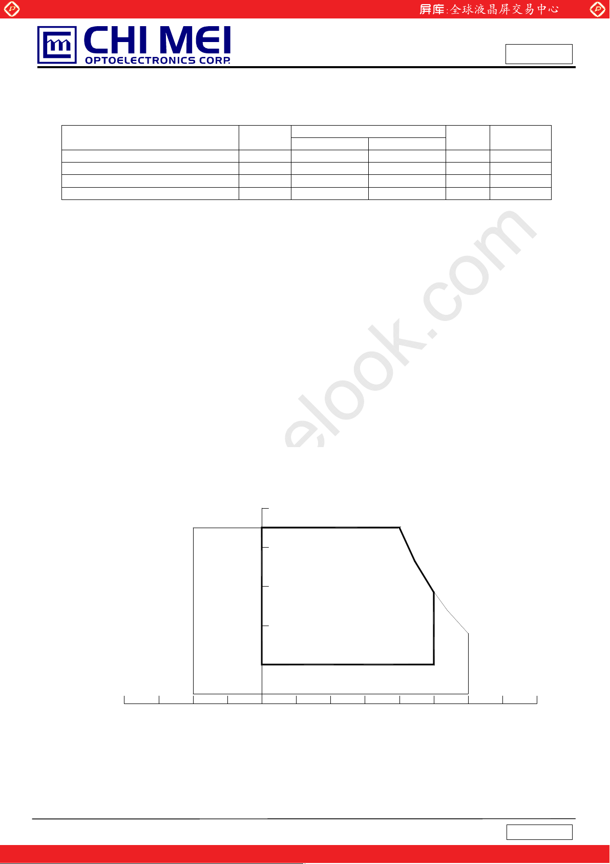
2.1 ABSOLUTE RATINGS OF ENVIRONMENT
Item Symbol
Storage Temperature TST -20 +60 ºC (1)
Operating Ambient Temperature TOP 0 +50 ºC (1), (2)
Shock (Non-Operating) S
Vibration (Non-Operating) V
Note (1) Temperature and relative humidity range is shown in the figure below.
(a) 90 %RH Max. (Ta Љ 40 ºC).
(b) Wet-bulb temperature should be 39 ºC Max. (Ta > 40 ºC).
(c) No condensation.
Note (2) The maximum operating temperature is based on the test condition that the surface temperature of
display area is less than or equal to 65 ºC with LCD module alone in a temperature controlled chamber.
www.panelook.com
Issued Date: Nov 7, 2006
Model No.: V320B1 - L04
Approval
Value
Min. Max.
- 50 G (3), (5)
NOP
- 1.0 G (4), (5)
NOP
Unit Note
Thermal management should be considered in final product design to prevent the surface temperature of
display area from being over 65 ºC. The range of operating temperature may degrade in case of improper
thermal management in final product design.
Note (3) 11 ms, half sine wave, 1 time for ± X, ± Y, ± Z.
Note (4) 10 ~ 200 Hz, 10 min, 1 time each X, Y, Z.
Note (5) At testing Vibration and Shock, the fixture in holding the module has to be hard and rigid enough
so that the module would not be twisted or bent by the fixture.
Relative Humidity (%RH)
100
90
80
60
Operating Range
40
20
10
Storage Range
Temperature (ºC)
6
One step solution for LCD / PDP / OLED panel application: Datasheet, inventory and accessory!
8060-20 400 20-40
Version 2.1
www.panelook.com
Page 9
Global LCD Panel Exchange Center
)
(1),
(3)
2.2 PACKAGE STORAGE
When storing modules as spares for a long time, the following precaution is necessary.
(a) Do not leave the module in high temperature, and high humidity for a long time. It is highly recommended to
store the module with temperature from 0 to 35кat normal humidity without condensation.
(b) The module shall be stored in dark place. Do not store the TFT-LCD module in direct sunlight or fluorescent
light.
2.3 ELECTRICAL ABSOLUTE RATINGS
2.3.1 TFT LCD MODULE
Item Symbol
Power Supply Voltage Vcc -0.3 6.0 V
Input Signal Voltage VIN -0.3 3.6 V
www.panelook.com
Value
Min. Max.
Issued Date: Nov 7, 2006
Model No.: V320B1 - L04
Approval
Unit Note
(1)
2.3.2 BACKLIGHT UNIT
Ё
Value
Unit Note
3000 V
Item Symbol
Lamp Vol t age V
Power Supply Voltage V
Control Signal Level
Note (1) Permanent damage to the device may occur if maximum values are exceeded. Functional
operation should be restricted to the conditions described under normal operating conditions.
Note (2) No moisture condensation or freezing.
Note (3) The control signals includes Backlight On/Off Control, Internal PWM Control, External PWM
Control and Internal/External PWM Selection.
030V(1
Ё
Min. Max.
-0.3 7 V
7
One step solution for LCD / PDP / OLED panel application: Datasheet, inventory and accessory!
Version 2.1
www.panelook.com
Page 10
Global LCD Panel Exchange Center
www.panelook.com
Issued Date: Nov 7, 2006
Model No.: V320B1 - L04
3. ELECTRICAL CHARACTERISTICS
3.1 TFT LCD MODULE Ta = 25 ± 2 ºC
Parameter Symbol
Min. Typ. Max.
Power Supply Voltage VCC 4.5 5.0 5.5 V (1)
Power Supply Ripple Voltage VRP - - 100 mV
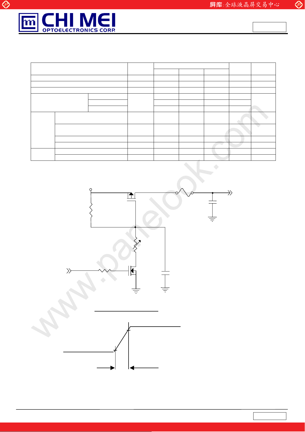
Rush Current I
- - 3.0 A (2)
RUSH
White - 1.50 1.87 A
Power Supply Current
Differential Input High
LVDS
Interface
Threshold Voltage
Differential Input Low
Threshold Voltage
Common Input Voltage V
Terminating Resistor R
Black - 1.00 - A
Vertical Stripe
I
CC
- 1.30 - A
- - +100 mV
V
LVT H
-100 - - mV
V
LVT L
1.125 1.25 1.375 V
LVC
- 100 - ohm
T
Input High Threshold Voltage VIH 2.7 - 3.3 V CMOS
interface
Input Low Threshold Voltage V
0 - 0.7 V
IL
Note (1) The module should be always operated within above ranges.
Value
Unit Note
Approval
(3)
Note (2) Measurement Conditions:
+5.0V
R1
1K
(Low to High)
(Control Signal)
SW
R2
1K
Vcc rising time is 470us
Q1 Si4485DY
47K
Q2
2N7002
VR1
+5V
C1
0.01uF
FUSE
C3
1uF
Vcc
(LCD Module Input)
0.9Vcc
0.1Vcc
GND
470us
8
One step solution for LCD / PDP / OLED panel application: Datasheet, inventory and accessory!
Version 2.1
www.panelook.com
Page 11
Global LCD Panel Exchange Center
(2)
(2)
Note (3) The specified power supply current is under the conditions at Vcc = 5 V, Ta = 25 ± 2 ºC, fv = 60 Hz,
whereas a power dissipation check pattern below is displayed.
www.panelook.com
Issued Date: Nov 7, 2006
Model No.: V320B1 - L04
Approval
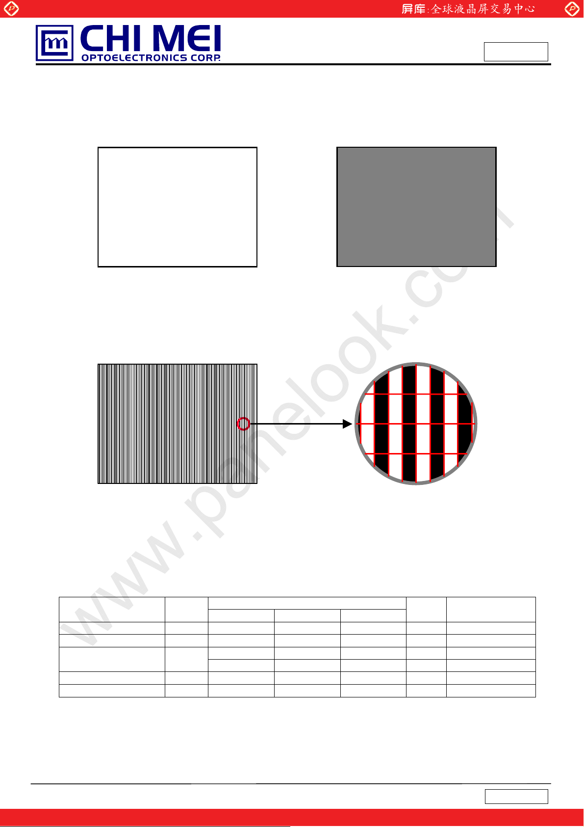
a. White Pattern
Active Area
c. Vertical Stripe Pattern
b. Black Pattern
Active Area
R
G
R
B
G
B
B
R
R
G
G
B
B
R
R
B
R R
Active Area
3.2 BACKLIGHT INVERTER UNIT
3.2.1 CCFL (Cold Cathode Fluorescent Lamp) CHARACTERISTICS (
Parameter Symbol
Lamp Voltage V
Lamp Current I
Lamp Starting Voltage V
Operating Frequency FO 40 - 70
Lamp Life Time LBL 50,000 60,000 -
W
L
S
Min. Typ. Max.
- 1280 -
4.3 4.8 5.3
- -
- -
Value
2440
2360
R
G
G
B
G
B
Ta = 2 5 ± 2 ºC )
V
mA
V
V
B
R
G
B
Unit Note
I
RMS
(1)
RMS
RMS
RMS
KHz (3)
Hrs (4)
= 4.8mA
L
, Ta = 0 ºC
, Ta = 25 ºC
9
One step solution for LCD / PDP / OLED panel application: Datasheet, inventory and accessory!
Version 2.1
www.panelook.com
Page 12
Global LCD Panel Exchange Center
g
A
A
A
A
A
A
A
A
A
A
A
A
A
A
A
A
3.2.2 INVERTER CHARACTERISTICS (Ta = 25 ± 2 ºC)
Parameter Symbol
Power Consumption PBL - 108 113 W (5),(6), IL = 4.8mA
Input Voltage VBL 22.8 24 25.2 V
Input Current IBL -4.5-A Non Dimmin
Input Ripple Noise - - - 500 mV
Backlight Turn on Voltage V
Oscillating Frequency FW 55 58 61 kHz
Dimming frequency FB 150 160 170 Hz
Minimum Duty Ratio D
Note (1) Lamp current is measured by utilizing high frequency current meters as shown below:
BS
MIN
www.panelook.com
Issued Date: Nov 7, 2006
Model No.: V320B1 - L04
Approval
Value
Min. Typ. Max.
2450
2360
--
--
15 20 25 %
Unit Note
DC
P-P
Ta = 0 º C
V
RMS
Ta = 25 ºC
V
RMS
VBL=22.8V
LCD
Module
LV (Black +)
LV (White,-)
HV (Pink)
HV (White)
HV (Pink)
HV (White)
HV (Pink)
HV (White)
HV (Pink)
HV (White)
HV (Pink)
HV (White)
HV (Pink)
HV (White)
HV (Pink)
HV (White)
HV (Pink)
HV (White)
1
2
1
2
1
2
1
2
Inverter
1
2
1
2
1
2
1
2
Note (2) The lamp starting voltage V
should be applied to the lamp for more than 1 second under starting
S
up duration. Otherwise the lamp could not be lighted on completed.
Note (3) The lamp frequency may produce interference with horizontal synchronous frequency of the
display input signals, and it may result in line flow on the display. In order to avoid interference, the
lamp frequency should be detached from the horizontal synchronous frequency and its harmonics
as far as possible.
Note (4) The life time of a lamp is defined as when the brightness is larger than 50% of its original value
and the effective discharge length is longer than 80% of its original length (Effective discharge
length is defined as an area that has equal to or more than 70% brightness compared to the
brightness at the center point of lamp.) as the time in which it continues to operate under the
10
One step solution for LCD / PDP / OLED panel application: Datasheet, inventory and accessory!
Version 2.1
www.panelook.com
Page 13
Global LCD Panel Exchange Center
yp
y
y
www.panelook.com
Issued Date: Nov 7, 2006
Model No.: V320B1 - L04
Approval
condition at Ta = 25 2к and IL = 4.3 ~ 5.3 mA
Note (5) The power supply capacity should be higher than the total inverter power consumption P
RMS
.
. Since
BL
the pulse width modulation (PWM) mode was applied for backlight dimming, the driving current
changed as PWM duty on and off. The transient response of power supply should be considered
for the changing loading when inverter dimming.
Note (6) The measurement condition of Max. value is based on 32" backlight unit under input voltage 24V,
average lamp current 5.3 mA and lighting 30 minutes later.
3.2.3 INVERTER INTERFACE CHARACTERISTICS
Parameter Symbol
Voltage
ON
OFF
V
HI
PWM Select Voltage
Control Voltage
Control Voltage
LO
MAX
MIN
HI 2.0
LO
V
V
Control Signal Rising Time T
Control Signal Falling Time T
PWM Signal Rising Time T
PWM Signal Falling Time T
Input impedance R
BLON Delay Time T
BLON Off Time T
BLON
V
SEL
IPWM
EPWM
V
Tes t
Condition
Ё
Ё
Ё
Ё
SEL
V
SEL
ЁЁЁ100 ms
ЁЁЁ100 ms
ЁЁЁ50 us
ЁЁЁ50 us
Ё 1 ЁЁMӨ
Ё 500 ЁЁms
Ё 500 ЁЁms
Min. T
= L
= H
Note (1) The SEL signal should be valid before backlight turns on by BLON signal. It is inhibited to change
Value
. Max.
2.0
0
2.0
0
Ё
Ё
Ё
Ё
ЁЁ
Ё
0
Ё
0
Ё
Unit Note
5.0 V On/Off Control
0.8 V
5.0 V Internal/External
0.8 V
3.0 V minimum dutyratioInternal PWM
Ё
V maximum dut
5.0 V duty on External PWM
0.8 V dut
ratio
fff
the internal/external PWM selection (SEL) during backlight turn on period.
Note (2) The power sequence and control signal timing are shown as the following figure.
11
One step solution for LCD / PDP / OLED panel application: Datasheet, inventory and accessory!
Version 2.1
www.panelook.com
Page 14
Global LCD Panel Exchange Center
BL
V
www.panelook.com
Issued Date: Nov 7, 2006
Model No.: V320B1 - L04
Approval
V
V
V
BLON
V
SEL
EPWM
IPWM
V
Toff
100%
2.0V
0.8V
2.0V
0.8V
2.0V
0.8V
3.0V
PWM
Period
Ton
Backlight on duration
Tr Tf
Ext. Dimming Function
PWMF
T
PWMR
T
Int. Dimming Function
External
PWM Duty
Minimun
Duty
0
0
0
0
0
W
External
12
One step solution for LCD / PDP / OLED panel application: Datasheet, inventory and accessory!
Version 2.1
www.panelook.com
Page 15

Global LCD Panel Exchange Center
q
(
)
q
4. BLOCK DIAGRAM
4.1 TFT LCD MODULE
www.panelook.com
Issued Date: Nov 7, 2006
Model No.: V320B1 - L04
Approval
RX0(+/-)
RX1(+/-)
RX2(+/-)
RX3(+/-)
RXCLK
Vcc
GND
E_PWM
I_PWM
BLON
+/-
VBL
GND
SEL
CN1
INPUT CONNECTOR
(JAE,FI-X30SSL-HF)
FRAME BUFFER
or e
TIMING
ual
INVERTER CONNECTOR
CN1:S14B-PH-SM3-TB(D)(LF)(JST)
or equal
CONTROLLER
DC/DC CONVERTER &
REFERENCE VOLTAGE
CN2: S2B-ZR-SM3A-TF (D)(LF)(JST) or equal
SCAN DRIVER IC
DATA DRIVER IC
CN3-CN10:
SM02 (8.0)B-BHS-1-TB(LF)(JST)
or e
ual
TFT LCD PANEL
(1366x3x768)
BACKLIGHT
UNIT
13
One step solution for LCD / PDP / OLED panel application: Datasheet, inventory and accessory!
Version 2.1
www.panelook.com
Page 16

Global LCD Panel Exchange Center
(2)
(3)
(5)
5. INTERFACE PIN CONNECTION
5.1 TFT LCD MODULE
CNF1 Connector Pin Assignment
Pin No. Sy
1 NC No Connection or Ground
2 RPF Display Rotation
3 SELLVDS Select LVDS data format
4 NC No Connection
5 NC No Connection
6 ODSEL Overdrive Lookup Table Selection
7 NC Ground
8 GND Ground
9 RX0- Negative transmission data of pixel 0
10 RX0+ Positive transmission data of pixel 0
11 RX1- Negative transmission data of pixel 1
12 RX1+ Positive transmission data of pixel 1
13 RX2- Negative transmission data of pixel 2
14 RX2+ Positive transmission data of pixel 2
15 RXCLK- Negative of clock
16 RXCLK+ Positive of clock
17 RX3- Negative transmission data of pixel 3
18 RX3+ Positive transmission data of pixel 3
19 GND Ground
20 NC No Connection or Ground
21 NC No Connection or Ground
22 NC No Connection or Ground
23 GND Ground
24 GND Ground
25 GND Ground
26 VCC Power supply: +5V
27 VCC Power supply: +5V
28 VCC Power supply: +5V
29 VCC Power supply: +5V
30 VCC Power supply: +5V
Note (1) Connector Part No.: FI-X30SSL-HF(JAE) or compatible
mbol Description Note
www.panelook.com
Issued Date: Jul 17, 2006
Model No.: V320B1 - L04
Approval
(4)
Note (2) Low or open: normal display (default), High : display with 180 degree rotation
Note (3) Please refer to 5.5 LVDS INTERFACE (Page 18)
Note (4) Reserved for internal use. Left it open.
Note (5) Overdrive lookup table selection. The Overdrive lookup table should be selected in accordance to the
frame rate to optimize image quality.
ODSEL Note
L or Open Lookup table was optimized for 60 Hz frame rate.
H Lookup table was optimized for 50 Hz frame rate.
14
One step solution for LCD / PDP / OLED panel application: Datasheet, inventory and accessory!
Version 2.1
www.panelook.com
Page 17

Global LCD Panel Exchange Center
5.2 BACKLIGHT UNIT
The pin configuration for the housing and leader wire is shown in the table below.
CN3-CN10 (Housing): BHR-03VS-1(JST) or equivalent
Pin No. Symbol Description
1 HV High Voltage Pink
2 HV High Voltage White
Note (1) The backlight interface housing for high voltage side is a model BHR-03VS-1, manufactured by JST or
www.panelook.com
Issued Date: Nov 7, 2006
Model No.: V320B1 - L04
Approval
Wire Color
equivalent
. The mating header on inverter part number is SM02(8.0)B-BHS-1-TB(LF)(JST).
CN2 (Housing): ZHR-2 (JST) or equivalent
Pin No. Symbol Description
1 LV Low Voltage (+) Black
2 LV Low Voltage (-) White
Note (2) The backlight interface housing and return cable for low voltage side is a model ZHR-2 , manufactured
by JST or equivalent. The mating header on inverter part number is S2B-ZR-SM3A-TF(D)(LF)(JST)
or equivalent.
Wire Color
8 Female Connectors
BHR-03VS-1(JST)
or Equal
1.HV(Pink,+)
2.HV(White,+)
1.HV(Pink,-)
2.HV(White,-)
1.HV(Pink,+)
2.HV(White,+)
15
1.HV(Pink,-)
2.HV(White,-)
1.HV(Pink,+)
2.HV(White,+)
1.HV(Pink,-)
2.HV(White,-)
1.HV(Pink,+)
2.HV(White,+)
1.HV(Pink,-)
2.HV(White,-)
ZHR-2 or Equal
Retruen cable
1.LV(White)
2.LV(White)
One step solution for LCD / PDP / OLED panel application: Datasheet, inventory and accessory!
Version 2.1
www.panelook.com
Page 18

Global LCD Panel Exchange Center
5.3 INVERTER UNIT
CN1(Header): S14B-PH-SM3-TB(D)(LF)(JST) or equivalent..
Pin No. Symbol Description
1
2
3
4
5 N.C. N.C.
6
7
8
9
10 N.C. N.C.
11 SEL
12 E_PWM
13 I_PWM
14 BLON Backlight on/off control
VBL +24V Power input
GND Ground
Internal/external PWM selection
High : external dimming
Low : internal dimming
External PWM control signal
E_PWM should be connected to ground when internal PWM was selected (SEL =
low).
Internal PWM control signal
I_PWM should be connected to ground when external PWM was selected (SEL =
high).
www.panelook.com
Issued Date: Nov 7, 2006
Model No.: V320B1 - L04
Approval
CN2(Header): S2B-ZR-SM3A-TF(D)(LF)(JST) or equivalent
Pin No. Symbol Description
1
2
CN3-CN8(Header): SM02(8.0)B-BHS-1-TB(LF)(JST) or equivalent.
Pin No. Symbol Description
1
2
Note (1) Floating of any control signal is not allowed.
CCFL COLD
CCFL COLD
CCFL HOT
CCFL HOT
CCFL low voltage (+)
CCFL low voltage (-)
CCFL high voltage
CCFL high voltage
16
One step solution for LCD / PDP / OLED panel application: Datasheet, inventory and accessory!
Version 2.1
www.panelook.com
Page 19

Global LCD Panel Exchange Center
G0-G
0
G0-G
p
5.4 BLOCK DIAGRAM OF INTERFACE
www.panelook.com
Issued Date: Nov 7, 2006
Model No.: V320B1 - L04
Approval
CNF1
R0-R7
7
-B7
B
DE
Host
Graphics
Controller
TxIN
PLL
LVDS Transmitter
THC63LVDM83A
(LVDF83A)
Rx0+
Rx
-
Rx1+
Rx1-
Rx2+
Rx2-
Rx3+
CLK+
51Ө
100pF
51Ө
51Ө
100
F
51Ө
51Ө
100pF
51Ө
51Ө
51Ө
51Ө
51Ө
100pF
100pF
PLL
-
-
RxOUT
R0-R7
7
B
-B7
DE
DCLK
Timing
Controller
LVDS Receiver
THC63LVDF84A
R0~R7 : Pixel R Data ,
G0~G7 : Pixel G Data ,
B0~B7 : Pixel B Data ,
DE : Data enable signal
Note (1) The system must have the transmitter to drive the module.
Note (2) LVDS cable impedance shall be 50 ohms per signal line or about 100 ohms per twist-pair line when it is
used differentially.
17
One step solution for LCD / PDP / OLED panel application: Datasheet, inventory and accessory!
Version 2.1
www.panelook.com
Page 20

Global LCD Panel Exchange Center
5.5 LVDS INTERFACE
www.panelook.com
Issued Date: Nov 7, 2006
Model No.: V320B1 - L04
Approval
SIGNAL
SELLVDS
=L or
R0
R1
R2
R3
R4
R5
G0
G1
G2
G3
G4
G5
B0
B1
24
bit
B2
B3
B4
B5
DE
R6
R7
G6
G7
B6
B7
RSVD 1
RSVD 2
RSVD 3
R0~R7: Pixel R Data (7; MSB, 0; LSB)
SELLVDS
OPEN
DCLK 31 TxCLK IN TxCLK OUT+
=H
R2
R3
R4
R5
R6
R7
G2
G3
G4
G5
G6
G7
B2
B3
B4
B5
B6
B7
DE
R0
R1
G0
G1
B0
B1
RSVD 1
RSVD 2
RSVD 3
TRANSMITTER
THC63LVDM83A
PIN INPUT Host TFT-LCD PIN OUTPUT
51
52
54
55
56
3
4
6
7
11
12
14
15
19
20
22
23
24
30
50
2
8
10
16
18
25
27
28
TxIN0
TxIN1
TxIN2
TxIN3
TxIN4
TxIN6
TxIN7
TxIN8
TxIN9
TxIN12
TxIN13
TxIN14
TxIN15
TxIN18
TxIN19
TxIN20
TxIN21
TxIN22
TxIN26
TxIN27
TxIN5
TxIN10
TxIN11
TxIN16
TxIN17
TxIN23
TxIN24
TxIN25
INTERFACE
CONNECTOR
TA OUT0+
TA OUT0-
TA OUT1+
TA OUT1-
TA OUT2+
TA OUT2-
TA OUT3+
TA OUT3-
TxCLK OUT-
Rx 0+
Rx 0-
Rx 1+
Rx 1-
Rx 2+
Rx 2-
Rx 3+
Rx 3-
RxCLK IN+
RxCLK IN-
RECEIVER
THC63LVDF84A
Rx OUT0
27
Rx OUT1
29
Rx OUT2
30
Rx OUT3
32
Rx OUT4
33
Rx OUT6
35
Rx OUT7
37
Rx OUT8
38
Rx OUT9
39
Rx OUT12
43
Rx OUT13
45
Rx OUT14
46
Rx OUT15
47
Rx OUT18
51
Rx OUT19
53
Rx OUT20
54
Rx OUT21
55
Rx OUT22
1
Rx OUT26
6
Rx OUT27
7
Rx OUT5
34
Rx OUT10
41
Rx OUT11
42
Rx OUT16
49
Rx OUT17
50
Rx OUT23
2
Rx OUT24
3
Rx OUT25
5
26 RxCLK OUT DCLK
TFT CONTROL
INPUT
SELLVDS
=L or
OPEN
R0
R1
R2
R3
R4
R5
G0
G1
G2
G3
G4
G5
B0
B1
B2
B3
B4
B5
DE
R6
R7
G6
G7
B6
B7
NC
NC
NC
SELLVDS
=H
R2
R3
R4
R5
R6
R7
G2
G3
G4
G5
G6
G7
B2
B3
B4
B5
B6
B7
DE
R0
R1
G0
G1
B0
B1
NC
NC
NC
G0~G7: Pixel G Data (7; MSB, 0; LSB)
B0~B7: Pixel B Data (7; MSB, 0; LSB)
DE : Data enable signal
Notes(1) RSVD(reserved)pins on the transmitter shall be “H” or( “L” or OPEN)
18
One step solution for LCD / PDP / OLED panel application: Datasheet, inventory and accessory!
Version 2.1
www.panelook.com
Page 21

Global LCD Panel Exchange Center
5.6 COLOR DATA INPUT ASSIGNMENT
The brightness of each primary color (red, green and blue) is based on the 8-bit gray scale data input for
the color. The higher the binary input, the brighter the color. The table below provides the assignment of
color versus data input.
Color
R7 R6 R5 R4 R3 R2 R1 R0 G7 G6 G5 G4 G3 G2 G1 G0 B7 B6 B5 B4 B3 B2 B1 B0
Black
Red
Green
Basic
Colors
Gray
Scale
Of
Red
Gray
Scale
Of
Green
Gray
Scale
Of
Blue
Note (1) 0: Low Level Voltage, 1: High Level Voltage
Blue
Cyan
Magenta
Ye ll ow
White
Red(0) / Dark
Red(1)
Red(2)
:
:
Red(253)
Red(254)
Red(255)
Green(0) / Dark
Green(1)
Green(2)
:
:
Green(253)
Green(254)
Green(255)
Blue(0) / Dark
Blue(1)
Blue(2)
:
:
Blue(253)
Blue(254)
Blue(255)
0
0
1
1
0
0
0
0
0
0
1
1
1
1
1
1
0
0
0
0
0
0
:
:
:
:
1
1
1
1
1
1
0
0
0
0
0
0
:
:
:
:
0
0
0
0
0
0
0
0
0
0
0
0
:
:
:
:
0
0
0
0
0
0
www.panelook.com
Issued Date: Nov 7, 2006
Model No.: V320B1 - L04
Approval
Data Signal
Red Green Blue
0
0
0
0
0
0
0
0
0
0
0
0
0
0
0
0
1
1
1
1
1
1
0
0
0
0
0
0
0
0
0
0
0
0
0
1
1
1
1
1
1
1
0
0
0
0
0
0
0
0
0
0
0
0
0
0
0
0
0
0
0
1
1
1
1
1
1
1
1
1
1
1
1
1
0
0
0
0
0
0
0
1
1
1
1
1
1
1
1
1
1
1
1
1
1
1
1
1
1
1
1
1
1
1
1
1
1
0
0
0
0
0
0
0
0
0
0
0
0
0
0
0
0
0
0
0
0
1
0
0
0
0
0
0
0
0
0
0
0
0
0
1
0
0
0
0
:
:
:
:
:
:
:
:
:
:
:
:
:
:
:
:
:
:
:
:
:
:
:
:
:
:
0
0
0
0
0
0
0
1
0
1
1
1
1
0
0
0
0
0
0
0
0
1
1
1
1
1
0
0
0
0
0
0
0
1
1
1
1
1
1
0
0
0
0
0
0
0
0
0
0
0
0
0
0
0
0
0
0
0
0
0
0
0
0
0
0
1
0
0
0
0
0
0
0
0
0
0
0
0
:
:
:
:
:
:
:
:
:
:
:
:
:
:
:
:
:
:
:
:
:
:
:
:
:
:
0
1
1
1
1
1
1
0
0
0
0
0
0
1
1
1
1
1
1
1
0
0
0
0
0
0
1
1
1
1
1
1
1
0
0
0
0
0
0
0
0
0
0
0
0
0
0
0
0
0
0
0
0
0
0
0
0
0
0
0
0
0
0
0
0
0
0
0
0
0
0
0
0
0
0
0
0
0
:
:
:
:
:
:
:
:
:
:
:
:
:
:
:
:
:
:
:
:
:
:
:
:
:
:
0
0
0
0
0
0
0
0
0
0
0
0
0
0
0
0
0
0
0
0
0
0
0
0
0
0
0
0
0
0
0
0
0
0
0
0
0
0
0
0
0
0
1
0
1
1
1
0
1
1
0
1
1
0
0
0
0
0
0
:
:
0
0
0
0
0
0
0
0
0
1
0
0
:
:
0
1
0
0
0
1
0
0
0
0
0
0
:
:
1
0
1
0
1
0
0
0
0
0
0
0
0
0
0
0
0
0
0
0
0
0
0
0
0
0
1
1
1
1
1
1
1
1
1
1
1
1
1
1
1
1
1
1
1
1
1
0
0
0
0
0
0
0
1
1
1
1
1
1
1
0
0
0
0
0
0
0
0
0
0
0
0
0
0
0
0
0
0
0
0
0
:
:
:
:
:
:
:
:
:
:
:
:
:
:
:
:
0
0
0
0
0
0
0
0
0
0
0
0
0
0
0
0
0
0
0
0
0
0
0
0
0
0
0
0
0
0
0
0
0
0
0
0
0
0
0
0
0
0
:
:
:
:
:
:
:
:
:
:
:
:
:
:
:
:
0
0
0
0
0
0
0
0
0
0
0
0
0
0
0
0
0
0
0
0
0
0
0
0
0
0
0
0
1
0
0
0
0
0
0
0
1
0
0
0
0
0
:
:
:
:
:
:
:
:
:
:
:
:
:
:
:
:
1
0
1
1
1
1
1
0
1
1
1
1
1
1
1
1
1
1
1
1
1
19
One step solution for LCD / PDP / OLED panel application: Datasheet, inventory and accessory!
Version 2.1
www.panelook.com
Page 22

Global LCD Panel Exchange Center
g
y
6. INTERFACE TIMING
6.1 INPUT SIGNAL TIMING SPECIFICATIONS
The input signal timing specifications are shown as the following table and timing diagram.
nal Item Symbol Min. Typ. Max. Unit Note
Si
Frequenc
LVDS Receiver Clock
Input cycle to
cycle jitter
www.panelook.com
Issued Date: Nov 7, 2006
Model No.: V320B1 - L04
Approval
1/Tc 60 86 88 MHZ
Trcl - - 200 ps
LVDS Receiver Data
Vertical Active Display Term
Horizontal Active Display Term
Note (1) Since this module is operated in DE only mode, Hsync and Vsync input signals should be set to
low logic level. Otherwise, this module would operate abnormally.
(2) Please refer to 5.1 for detail information.
Setup Time Tlvsu 600 - - ps
Hold Time Tlvhd 600 - - ps
Frame Rate
Total Tv 778 795 888 Th Tv=Tvd+Tvb
Display Tvd 768 768 768 Th Blank Tvb 10 27 120 Th Total Th 1442 1798 1936 Tc Th=Thd+Thb
Display Thd 1366 1366 1366 Tc Blank Thb 76 432 570 Tc -
Fr5 47 50 53 Hz
Fr
6 57 60 63 Hz
(2)
INPUT SIGNAL TIMING DIAGRAM
Tv
Tvd
Tvb
DE
DCLK
DE
DATA
Th
Tc
Thd
Thb
Valid display data (1366 clocks)
20
Version 2.1
One step solution for LCD / PDP / OLED panel application: Datasheet, inventory and accessory!
www.panelook.com
Page 23

Global LCD Panel Exchange Center
LVDS RECEIVER INTERFACE TIMING DIAGRAM
RXCLK+/-
RXn+/-
www.panelook.com
Issued Date: Nov 7, 2006
Model No.: V320B1 - L04
Approval
Tc
Tlvsu
Tlvhd
1T
14
3T
14
5T
14
7T
14
9T
14
11T
14
13T
14
21
One step solution for LCD / PDP / OLED panel application: Datasheet, inventory and accessory!
Version 2.1
www.panelook.com
Page 24

Global LCD Panel Exchange Center
Љ
Љ
Љ
Љ
Љ
Љ
Љ
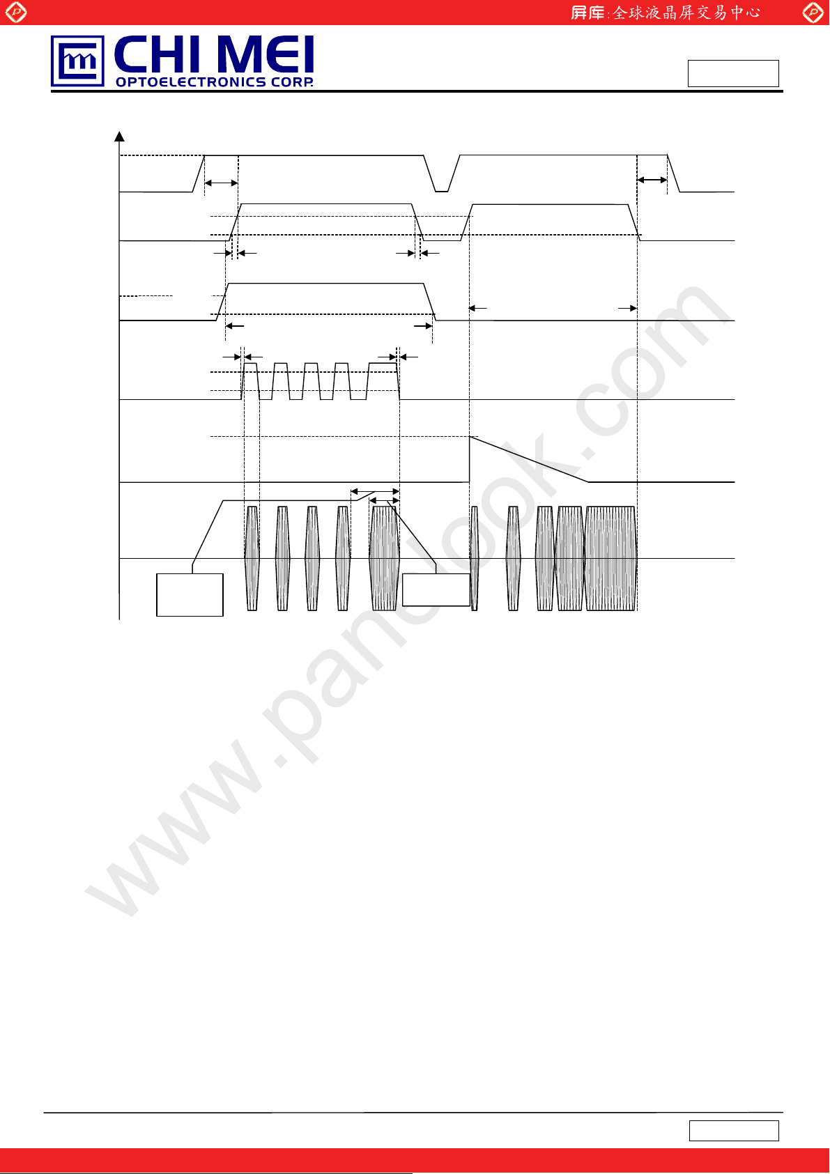
6.2 POWER ON/OFF SEQUENCE
To prevent a latch-up or DC operation of LCD module, the power on/off sequence should be as the
diagram below.
www.panelook.com
Issued Date: Nov 7, 2006
Model No.: V320B1 - L04
Approval
Power Supply
V
0.5ЉT1Љ10ms
0
0
500ms
CC
0V
T
2
50ms
T
3
50ms
T
4
Signals
0V
Backlight (Recommended)
500ms
100ms
T
5
T6
0.9 VCC
CC
0.1V
Power On
CC
0.9 V
0.1Vcc
T
3T1
2
T
T4
VALID
Power Off
50%
5
T
50%
6
T
Power ON/OFF Sequence
Note (1) The supply voltage of the external system for the module input should follow the definition of Vcc.
Note (2) Apply the lamp voltage within the LCD operation range. When the backlight turns on before the LCD
operation or the LCD turns off before the backlight turns off, the display may momentarily become
abnormal screen.
Note (3) In case of Vcc is in off level, please keep the level of input signals on the low or high impedance.
Note (4) T4 should be measured after the module has been fully discharged between power off and on period.
Note (5) Interface signal shall not be kept at high impedance when the power is on.
22
One step solution for LCD / PDP / OLED panel application: Datasheet, inventory and accessory!
Version 2.1
www.panelook.com
Page 25

Global LCD Panel Exchange Center
y
(2)
/
A
/
(7)
(5)
y
y
y
y
7. OPTICAL CHARACTERISTICS
7.1 TEST CONDITIONS
Item Symbol Value Unit
Ambient Temperature Ta
Ambient Humidity Ha
Supply Voltage VCC 5.0 V
Input Signal According to typical value in "3. ELECTRICAL CHARACTERISTICS"
Lamp Current I
Oscillating Frequency (Inverter) F
Frame rate 60 Hz
7.2 OPTICAL SPECIFICATIONS
The relative measurement methods of optical characteristics are shown in 7.2. The following items should
www.panelook.com
L
W
4.8mA r 0.5
25r2
50r10
58r3
Issued Date: Nov 7, 2006
Model No.: V320B1 - L04
Approval
o
C
%RH
mA
KHz
be measured under the test conditions described in 7.1 and stable environment shown in Note (6).
Item S
Contrast Ratio CR 900 1200
Response Time
Center Luminance of White L
verage Luminance of White L
White Variation
Cross Talk CT - - 4.0 %
Red
Green
Color
Chromaticity
Viewing
Angle
Blue
White
Color Gamut CG
Horizontal
Ver t ic a l
mbol Condition Min. Typ. Max. Unit Note
-
Gray to gray
average
350 400
GW
Rx 0.652 -
0.333 -
R
Gx 0.275 -
0.595 -
G
Bx 0.143 -
0.063 -
B
Wx 0.285 W
T
+
T
-
T
+
-
T
T
=0q, TY =0q
x
Viewing Normal
Angle
CRt20
- 6.5 12 ms (3)
400 500
- - 1.3 -
Typ
-0.03
0.293
72 75 % NTSC
80 88 80 88 80 88 80 88 -
-
-
Typ
+0.03
-
cd
cd
-
Deg
.
(4)
(6)
(1)
23
One step solution for LCD / PDP / OLED panel application: Datasheet, inventory and accessory!
Version 2.1
www.panelook.com
Page 26

Global LCD Panel Exchange Center
T
Note (1) Definition of Viewing Angle (Tx, Ty):
Viewing angles are measured by EZ-Contrast 160R (Eldim)
www.panelook.com
Issued Date: Nov 7, 2006
Model No.: V320B1 - L04
Approval
Normal
Tx = Ty = 0º
Ty- Ty
TX- = 90º
6 o’clock
T
y- = 90º
x-
y-
Note (2) Definition of Contrast Ratio (CR):
The contrast ratio can be calculated by the following expression.
Contrast Ratio (CR) = L255 / L0
L255: Luminance of gray level 255
L 0: Luminance of gray level 0
CR = CR (5), where CR (X) is corresponding to the Contrast Ratio of the point X at the figure in
Note (7).
Tx
Tx
12 o’clock direction
y+
T
y+ = 90º
x+
TX+ = 90º
Note (3) Definition of Gray to Gray Switching Time :
100%
90%
Optical
Response
10%
0%
Gray to gray
switching time
24
Gray to gray
switching time
ime
Version 2.1
One step solution for LCD / PDP / OLED panel application: Datasheet, inventory and accessory!
www.panelook.com
Page 27

Global LCD Panel Exchange Center
A
(
)
A
(
)
(
)
www.panelook.com
The driving signal means the signal of gray level 0, 63, 127, 191, 255.
Gray to gray average time means the average switching time of gray level 0 ,63,127,191,255 to each
other .
Issued Date: Nov 7, 2006
Model No.: V320B1 - L04
Approval
Note (4) Definition of Luminance of White (L
Measure the luminance of gray level 255 at center point and 5 points
L
= L (5)
C
L
= [L (1)+ L (2)+ L (3)+ L (4)+ L (5)] / 5
AVE
where L (x) is corresponding to the luminance of the point X at the figure in Note (7).
Note (5) Definition of Cross Talk (CT):
CT = | Y
– YA | / YAu 100 (%)
B
Where:
Y
= Luminance of measured location without gray level 0 pattern (cd/m2)
A
Y
= Luminance of measured location with gray level 0 pattern (cd/m2)
B
ctive Area
Gray 128
Y
Y
D,W
A, U
A, R
Y
(D/8,W/2)
A, L
Y
(D/2,7W/8)
A, D
(0, 0)
, L
):
C
AVE
(D/2,W/8)
(7D/8,W/2)
(D/4,W/4)
Y
(D/8,W/2)
B, L
Y
(D/2,7W/8)
B, D
0, 0
ctive Area
Gray 0
Gray 0
Gray 128
Y
(D/2,W/8)
B, U
Y
(7D/8,W/2)
B, R
(3D/4,3W/4)
D,W
25
One step solution for LCD / PDP / OLED panel application: Datasheet, inventory and accessory!
Version 2.1
www.panelook.com
Page 28

Global LCD Panel Exchange Center
Note (6) Measurement Setup:
The LCD module should be stabilized at given temperature for 1 hour to avoid abrupt temperature
change during measuring. In order to stabilize the luminance, the measurement should be
executed after lighting Backlight for 1 hour in a windless room.
LCD Module
LCD Panel
www.panelook.com
Issued Date: Nov 7, 2006
Model No.: V320B1 - L04
Approval
Center of the Screen
Note (7) Definition of White Variation (GW):
Measure the luminance of gray level 255 at 5 points
GW = Maximum [L (1), L (2), L (3), L (4), L (5)] / Minimum [L (1), L (2), L (3), L (4), L (5)]
Display Color Analyzer
(Minolta CA210)
Light Shield Room
(Ambient Luminance < 2 lux)
Horizontal Line
D
D/4 D/2 3D/4
12
X
5
: Test Point
X=1 to 5
W
W/4
W/2
Vertical Line
3W/4
One step solution for LCD / PDP / OLED panel application: Datasheet, inventory and accessory!
34
Active Area
26
Version 2.1
www.panelook.com
Page 29

Global LCD Panel Exchange Center
8. DEFINITION OF LABELS
8.1 CMO MODULE LABEL
The barcode nameplate is pasted on each module as illustration, and its definitions are as following explanation.
www.panelook.com
Issued Date: Nov 7, 2006
Model No.: V320B1 - L04
Approval
CHI MEI
OPTOELECTRONICS
(a) Model Name: V320B1-L04
(b) Revision: Rev. XX, for example: A0, A1… B1, B2… or C1, C2…etc.
(c) Serial ID: X X
X X X X X Y M D L N N N N
V320B1 -L04 Rev. XX
X X X X X X X Y M D L N N N N
Serial No.
Product Line
Year, Month, Date
CMO Internal Use
CMO Internal Use
Revision
E207943
MADE IN TAIWAN
Serial ID includes the information as below:
(a) Manufactured Date: Year: 0~9, for 2000~2009
Month: 1~9, A~C, for Jan. ~ Dec.
Day: 1~9, A~Y, for 1
(b) Revision Code: Cover all the change
(c) Serial No.: Manufacturing sequence of product
(d) Product Line: 1 -> Line1, 2 -> Line 2, …etc.
CMO Internal Use
st
to 31st, exclude I ,O, and U.
27
One step solution for LCD / PDP / OLED panel application: Datasheet, inventory and accessory!
Version 2.1
www.panelook.com
Page 30

Global LCD Panel Exchange Center
9. PACKAGING
9.1 PACKING SPECIFICATIONS
(1) 4 LCD TV modules / 1 Box
(2) Box dimensions : 906(L) X 384 (W) X 580 (H)
(3) Weight : approximately 31.5Kg ( 4 modules per box)
9.2 PACKING METHOD
Figures 9-1 and 9-2 are the packing method
LCD TV Module
www.panelook.com
Issued Date: Nov 7, 2006
Model No.: V320B1 - L04
Approval
Anti-static Bag
Cushion(Bottom)
Carton
2 pcs Drier
Carton Label
Figure.9-1 packing method
28
One step solution for LCD / PDP / OLED panel application: Datasheet, inventory and accessory!
Version 2.1
www.panelook.com
Page 31

Global LCD Panel Exchange Center
www.panelook.com
Issued Date: Nov 7, 2006
Model No.: V320B1 - L04
Approval
Air Transportation
Corner Protector:L1130*50mm*50mm
Pallet:L950*W1180*H140mm
Pallet Stack:L950*W1180*H1300mm
Gross:182kg
PP Belt
Figure. 9-2 Packing method
PE Sheet
Carton Label
29
One step solution for LCD / PDP / OLED panel application: Datasheet, inventory and accessory!
Version 2.1
www.panelook.com
Page 32

Global LCD Panel Exchange Center
www.panelook.com
Issued Date: Nov 7, 2006
Model No.: V320B1 - L04
Approval
10. PRECAUTIONS
10.1 ASSEMBLY AND HANDLING PRECAUTIONS
(1) Do not apply rough force such as bending or twisting to the module during assembly.
(2) It is recommended to assemble or to install a module into the user’s system in clean working areas.
The dust and oil may cause electrical short or worsen the polarizer.
(3) Do not apply pressure or impulse to the module to prevent the damage of LCD panel and backlight.
(4) Always follow the correct power-on sequence when the LCD module is turned on. This can prevent the
damage and latch-up of the CMOS LSI chips.
(5) Do not plug in or pull out the I/F connector while the module is in operation.
(6) Do not disassemble the module.
(7) Use a soft dry cloth without chemicals for cleaning, because the surface of polarizer is very soft and
easily scratched.
(8) Moisture can easily penetrate into LCD module and may cause the damage during operation.
(9) High temperature or humidity may deteriorate the performance of LCD module. Please store LCD
modules in the specified storage conditions.
(10) When ambient temperature is lower than 10ºC, the display quality might be reduced. For example, the
response time will become slow, and the starting voltage of CCFL will be higher than that of room
temperature.
10.2 SAFETY PRECAUTIONS
(1) The startup voltage of a backlight is over 1000 Volts. It may cause an electrical shock while assembling
with the inverter. Do not disassemble the module or insert anything into the backlight unit.
(2) If the liquid crystal material leaks from the panel, it should be kept away from the eyes or mouth. In
case of contact with hands, skin or clothes, it has to be washed away thoroughly with soap.
(3) After the module’s end of life, it is not harmful in case of normal operation and storage.
11. REGULATORY STANDARDS
11.1 SAFETY
Item Standard
UL UL 60950-1: 2003
UL UL 60065: 2003
cUL CAN/CSA C22.2 No.60950-1-03
cUL CAN/CSA C22.2 No.60065-03
CB IEC 60950-1:2001
CB IEC 60065:2001
30
One step solution for LCD / PDP / OLED panel application: Datasheet, inventory and accessory!
Version 2.1
www.panelook.com
Page 33

Global LCD Panel Exchange Center
12. MECHANICAL CHARACTERISTICS
www.panelook.com
Issued Date: Nov 7, 2006
Model No.: V320B1 - L04
Approval
࡛ભሽٝڶૻֆ
%*+/'+
31
One step solution for LCD / PDP / OLED panel application: Datasheet, inventory and accessory!
Version 2.1
www.panelook.com
Page 34

Global LCD Panel Exchange Center
www.panelook.com
Issued Date: Nov 7, 2006
Model No.: V320B1 - L04
Approval
࡛ભሽٝڶૻֆ
%*+/'+
32
One step solution for LCD / PDP / OLED panel application: Datasheet, inventory and accessory!
Version 2.1
www.panelook.com
Page 35

Global LCD Panel Exchange Center
www.panelook.com
One step solution for LCD / PDP / OLED panel application: Datasheet, inventory and accessory!
www.panelook.com
Page 36

Global LCD Panel Exchange Center
www.panelook.com
˥˘ˣˢ˥˧ʳˡˢˁ˞˔˂˅˃˃ˉ˂ˈ˃˅ˈˌ˔ˀ˄
˗˔˧˘ˍ˅˃˃ˉ˂ˈ˂ˌ
ˣ˔˚˘ˍʳʳʳʳʳʳʳʳ˄˂˄˄
Chemical Laboratory - KAO.,SGS Taiwan Ltd.
TEST REPORT
APPLICANT
Chi Mei Optoelectronics Corp.
No.1, Chi-Yeh Rd.,Hsin-Shin Village
Tainan Country 744, Taiwan, R.O.C
SAMPLE DESCRIPTION
One(1) group of submitted samples said to be
Sample Description LCD
Item Name
Sample Received
Testing Date
============================================================================================
:
:
:
:
V320B1-L04
APR 10, 2006
APR 25, 2006
This Test Report is issued by the Company subject to its General Conditions of Service printed overleaf. Attention is drawn to the limitations of liability, indemnification,
and Jurisdictional issues defined therein. The results shown in this test report refer only to the sample(s) tested unless otherwise stated. This Test Report cannot be
reproduced, except in full, without prior written permission of the Company. ڼܫᙅ༛ءֆૡࡳհຏشࣚ೭යཱིࢬ፹܂࿇࣋Ζᓮࣹრڼයཱི٨ٱ࣍હ૿Δലءֆ
հᆠ೭Δ܍ຂΔጥᝤᦞઃࣔᒔᒤհΖڼܫ࣠ೈڶᎅࣔႛኙᛀ᧭հᑌຂΖءܫآᆖءֆ૿ױΔլױຝٝᓤ፹Ζ
SGS Taiwan Ltd. No. 208, Chung Hwa 2nd Road, San Ming District, Kaohsiung, Taiwan / ଯѱΟ҇ύΒၡ208 ဦ
ѠᔠᡍࣽמިҽԖϦљ! t (886-7) 323-0920 f (886-7) 315-7484 www.sgs.com.tw
MemberoftheSGSGroup
One step solution for LCD / PDP / OLED panel application: Datasheet, inventory and accessory!
www.panelook.com
Page 37

Global LCD Panel Exchange Center
(A) Test Part
Item NO.
NO.1
NO.2
NO.3
NO.4
NO.5
NO.6
NO.7
NO.8
NO.9
NO.10
NO.11
NO.12
NO.13
NO.14
NO.15
NO.16
NO.17
NO.18
NO.19
NO.20
NO.21
NO.22
NO.23
NO.24
NO.25
NO.26
NO.27
NO.28
NO.29
NO.30
www.panelook.com
Item Name
Metal Frame
Screw 1
Screw 2
Silicone Pad
Double Tape 1
Tape 1/Tape 2
Film 1
PCB Cover
Screw 3
PCBA-C
Label 1
Inverter Cover
Screw 4
Mylar 1
DC/AC Inverter
Standoff
Screw 5
Rear Case
Mylar 2
Lamp Holder
Lamp Supporter
Lamp PCB
Wire 1
Wire 2
Tape 3
Rubber Cap
PCBA-X( L )
Label 2
PCBA-X( R )
Label 3
˥˘ˣˢ˥˧ʳˡˢˁ˞˔˂˅˃˃ˉ˂ˈ˃˅ˈˌ˔ˀ˄
˗˔˧˘ˍ˅˃˃ˉ˂ˈ˂ˌ
ˣ˔˚˘ˍʳʳʳʳʳʳʳʳ˅˂˄˄
Report No.
KA/2005/62742
KA/2005/90094
KA/2005/A0907
KA/2005/91203
KA/2005/51378
KA/2006/41355
KA/2006/40568
KA/2005/62742
KA/2005/A0907
KA/2006/41356
KA/2005/B0520
KA/2005/62742
KA/2005/B0332
KA/2005/70123
KA/2006/40569
KA/2006/41746
KA/2005/A0907
KA/2005/62742
KA/2005/70123
KA/2006/40570
KA/2006/41745
KA/2006/41357
KA/2006/10329
KA/2006/10331
KA/2006/41358
KA/2006/41359
KA/2006/41360
KA/2005/B0520
KA/2006/41361
KA/2005/B0520
This Test Report is issued by the Company subject to its General Conditions of Service printed overleaf. Attention is drawn to the limitations of liability, indemnification,
and Jurisdictional issues defined therein. The results shown in this test report refer only to the sample(s) tested unless otherwise stated. This Test Report cannot be
reproduced, except in full, without prior written permission of the Company. ڼܫᙅ༛ءֆૡࡳհຏشࣚ೭යཱིࢬ፹܂࿇࣋Ζᓮࣹრڼයཱི٨ٱ࣍હ૿Δലءֆ
հᆠ೭Δ܍ຂΔጥᝤᦞઃࣔᒔᒤհΖڼܫ࣠ೈڶᎅࣔႛኙᛀ᧭հᑌຂΖءܫآᆖءֆ૿ױΔլױຝٝᓤ፹Ζ
SGS Taiwan Ltd. No. 208, Chung Hwa 2nd Road, San Ming District, Kaohsiung, Taiwan / ଯѱΟ҇ύΒၡ208 ဦ
ѠᔠᡍࣽמިҽԖϦљ! t (886-7) 323-0920 f (886-7) 315-7484 www.sgs.com.tw
MemberoftheSGSGroup
One step solution for LCD / PDP / OLED panel application: Datasheet, inventory and accessory!
www.panelook.com
Page 38

Global LCD Panel Exchange Center
www.panelook.com
˥˘ˣˢ˥˧ʳˡˢˁ˞˔˂˅˃˃ˉ˂ˈ˃˅ˈˌ˔ˀ˄
˗˔˧˘ˍ˅˃˃ˉ˂ˈ˂ˌ
ˣ˔˚˘ˍʳʳʳʳʳʳʳʳˆ˂˄˄
Item NO.
NO.31
NO.32
NO.33
NO.34
*NO.35
*NO.36
*NO.37
*NO.38
*NO.39
*NO.40
*NO.41
*NO.42
Item Name
PCBA-Y
Label 4
Label 5
Film 2
Double Tape 2
Plastic Housing
Film 3
Film 4
Film 5
Double Tape 3
FFC 1
Label 6
*NO.43 FFC 2
*NO.44
*NO.45
CCFL
Wire 3
*NO.46 Wire 4
*NO.47
*NO.48
*NO.49
*NO.50
Connector
COF, Data Driver IC 1
Screw 6
COF, Data Driver IC 2
*NO.51 Screw 7
*NO.52 COF, Data Driver IC 3
*NO.53 Screw 8
*NO.54
Polarizer 1
*NO.55 Polarizer 2
*NO.56
Glass 1
*NO.57 Glass 2
*NO.58
Label 7
Report No.
KA/2006/41362
KA/2005/B0520
KA/2006/10996
KA/2006/40567
C511236
THJ0014811
THJ0002843
THJ0002843
THJ0002643
C511236
THJ0002364
THJ0006299
THJ0002364
C512007
C511244
C511244
THJ0016316
C511262
THJ0014881
C511262
THJ0014881
C511262
THJ0014881
C514098
THJ0009271
THJ0013511
THJ0013512
THJ0007284
Remark: * = The test result was offered by Intertek Testing Services TaiwanLtd
& TÜV RHEINLAND TAIWAN LTD.
This Test Report is issued by the Company subject to its General Conditions of Service printed overleaf. Attention is drawn to the limitations of liability, indemnification,
and Jurisdictional issues defined therein. The results shown in this test report refer only to the sample(s) tested unless otherwise stated. This Test Report cannot be
reproduced, except in full, without prior written permission of the Company. ڼܫᙅ༛ءֆૡࡳհຏشࣚ೭යཱིࢬ፹܂࿇࣋Ζᓮࣹრڼයཱི٨ٱ࣍હ૿Δലءֆ
հᆠ೭Δ܍ຂΔጥᝤᦞઃࣔᒔᒤհΖڼܫ࣠ೈڶᎅࣔႛኙᛀ᧭հᑌຂΖءܫآᆖءֆ૿ױΔլױຝٝᓤ፹Ζ
SGS Taiwan Ltd. No. 208, Chung Hwa 2nd Road, San Ming District, Kaohsiung, Taiwan / ଯѱΟ҇ύΒၡ208 ဦ
ѠᔠᡍࣽמިҽԖϦљ! t (886-7) 323-0920 f (886-7) 315-7484 www.sgs.com.tw
MemberoftheSGSGroup
One step solution for LCD / PDP / OLED panel application: Datasheet, inventory and accessory!
www.panelook.com
Page 39

Global LCD Panel Exchange Center
pp
g
pp
g
pp
g
pp
g
pp
g
pp
g
pp
g
pp
g
pp
g
pp
g
pp
g
1. Cd (Cadmium)
Unit NO.2 NO.3 NO.4 NO.5
m n.d. n.d. n.d. n.d.
m
% n.d. n.d. n.d. n.d.
Unit NO.7 NO.8 NO.9 NO.10
m n.d. n.d. n.d. n.d.
m
% n.d. n.d. n.d. n.d.
Unit NO.12 NO.13 NO.14 NO.15
m n.d. n.d. n.d. n.d.
m
% n.d. n.d. n.d. n.d.
Unit NO.17 NO.18 NO.19 NO.20
m n.d. n.d. n.d. n.d.
m
% n.d. n.d. n.d. n.d.
Unit NO.22 NO.23 NO.24 NO.25
m n.d. n.d. n.d. n.d.
m
% n.d. n.d. n.d. n.d.
Unit NO.27 NO.28 NO.29 NO.30
m n.d. n.d. n.d. n.d.
m
% n.d. n.d. n.d. n.d.
Unit NO.32 NO.33 NO.34 *NO.35
m n.d. n.d. n.d. n.d.
m
% n.d. n.d. n.d. n.d.
Unit *NO.37 *NO.38 *NO.39 *NO.40
m n.d. n.d. n.d. n.d.
m
% n.d. n.d. n.d. n.d.
Unit *NO.42 *NO.43 *NO.44 *NO.45
m n.d. n.d. n.d. n.d.
m
% n.d. n.d. n.d. n.d.
Unit *NO.47 *NO.48 *NO.49 *NO.50
m n.d. n.d. n.d. n.d.
m
% n.d. n.d. n.d. n.d.
Unit *NO.52 *NO.53 *NO.54 *NO.55
m n.d. n.d. n.d. n.d.
m
% n.d. n.d. n.d. n.d.
NO.1
n.d.
n.d.
n.d.
NO.6
n.d.
n.d.
n.d.
NO.11
n.d.
n.d.
n.d.
NO.16
n.d.
n.d.
n.d.
NO.21
n.d.
n.d.
n.d.
NO.26
n.d.
n.d.
n.d.
NO.31
n.d.
n.d.
n.d.
*NO.36
n.d.
n.d.
n.d.
*NO.41
n.d.
n.d.
n.d.
*NO.46
n.d.
n.d.
n.d.
*NO.51
n.d.
n.d.
n.d.
www.panelook.com
˥˘ˣˢ˥˧ʳˡˢˁ˞˔˂˅˃˃ˉ˂ˈ˃˅ˈˌ˔ˀ˄
˗˔˧˘ˍ˅˃˃ˉ˂ˈ˂ˌ
ˣ˔˚˘ˍʳʳʳʳʳʳʳʳˇ˂˄˄
n.d. n.d. n.d. n.d.
n.d. n.d. n.d. n.d.
n.d. n.d. n.d. n.d.
n.d. n.d. n.d. n.d.
n.d. n.d. n.d. n.d.
n.d. n.d. n.d. n.d.
n.d. n.d. n.d. n.d.
n.d. n.d. n.d. n.d.
n.d. n.d. n.d. n.d.
n.d. n.d. n.d. n.d.
n.d. n.d. n.d. n.d.
This Test Report is issued by the Company subject to its General Conditions of Service printed overleaf. Attention is drawn to the limitations of liability, indemnification,
and Jurisdictional issues defined therein. The results shown in this test report refer only to the sample(s) tested unless otherwise stated. This Test Report cannot be
reproduced, except in full, without prior written permission of the Company. ڼܫᙅ༛ءֆૡࡳհຏشࣚ೭යཱིࢬ፹܂࿇࣋Ζᓮࣹრڼයཱི٨ٱ࣍હ૿Δലءֆ
հᆠ೭Δ܍ຂΔጥᝤᦞઃࣔᒔᒤհΖڼܫ࣠ೈڶᎅࣔႛኙᛀ᧭հᑌຂΖءܫآᆖءֆ૿ױΔլױຝٝᓤ፹Ζ
ѠᔠᡍࣽמިҽԖϦљ! t (886-7) 323-0920 f (886-7) 315-7484 www.sgs.com.tw
One step solution for LCD / PDP / OLED panel application: Datasheet, inventory and accessory!
SGS Taiwan Ltd. No. 208, Chung Hwa 2nd Road, San Ming District, Kaohsiung, Taiwan / ଯѱΟ҇ύΒၡ208 ဦ
MemberoftheSGSGroup
www.panelook.com
Page 40

Global LCD Panel Exchange Center
pp
g
pp
g
pp
g
pp
g
pp
g
pp
g
pp
g
pp
g
pp
g
pp
g
www.panelook.com
˥˘ˣˢ˥˧ʳˡˢˁ˞˔˂˅˃˃ˉ˂ˈ˃˅ˈˌ˔ˀ˄
˗˔˧˘ˍ˅˃˃ˉ˂ˈ˂ˌ
ˣ˔˚˘ˍʳʳʳʳʳʳʳʳˈ˂˄˄
Unit *NO.57 *NO.58
m n.d. n.d.
m
% n.d. n.d.
+6
2. Cr
(Hexavalent-Chromium)
Unit NO.2 NO.3 NO.4 NO.5
m n.d. n.d. n.d. n.d.
m
% n.d. n.d. n.d. n.d.
Unit NO.7 NO.8 NO.9 NO.10
m n.d. n.d. n.d. n.d.
m
% n.d. n.d. n.d. n.d.
Unit NO.12 NO.13 NO.14 NO.15
m n.d. n.d. n.d. n.d.
m
% n.d. n.d. n.d. n.d.
Unit NO.17 NO.18 NO.19 NO.20
m n.d. n.d. n.d. n.d.
m
% n.d. n.d. n.d. n.d.
Unit NO.22 NO.23 NO.24 NO.25
m n.d. n.d. n.d. n.d.
m
% n.d. n.d. n.d. n.d.
Unit NO.27 NO.28 NO.29 NO.30
m n.d. n.d. n.d. n.d.
m
% n.d. n.d. n.d. n.d.
Unit NO.32 NO.33 NO.34 *NO.35
m n.d. n.d. n.d. n.d.
m
% n.d. n.d. n.d. n.d.
Unit *NO.37 *NO.38 *NO.39 *NO.40
m n.d. n.d. n.d. n.d.
m
% n.d. n.d. n.d. n.d.
Unit *NO.42 *NO.43 *NO.44 *NO.45
m n.d. n.d. n.d. n.d.
m
% n.d. n.d. n.d. n.d.
*NO.56
n.d.
n.d.
n.d.
NO.1
n.d.
n.d.
n.d.
NO.6
n.d.
n.d.
n.d.
NO.11
n.d.
n.d.
n.d.
NO.16
n.d.
n.d.
n.d.
NO.21
n.d.
n.d.
n.d.
NO.26
n.d.
n.d.
n.d.
NO.31
n.d.
n.d.
n.d.
*NO.36
n.d.
n.d.
n.d.
*NO.41
n.d.
n.d.
n.d.
n.d. n.d.
n.d. n.d. n.d. n.d.
n.d. n.d. n.d. n.d.
n.d. n.d. n.d. n.d.
n.d. n.d. n.d. n.d.
n.d. n.d. n.d. n.d.
n.d. n.d. n.d. n.d.
n.d. n.d. n.d. n.d.
n.d. n.d. n.d. n.d.
n.d. n.d. n.d. n.d.
This Test Report is issued by the Company subject to its General Conditions of Service printed overleaf. Attention is drawn to the limitations of liability, indemnification,
and Jurisdictional issues defined therein. The results shown in this test report refer only to the sample(s) tested unless otherwise stated. This Test Report cannot be
reproduced, except in full, without prior written permission of the Company. ڼܫᙅ༛ءֆૡࡳհຏشࣚ೭යཱིࢬ፹܂࿇࣋Ζᓮࣹრڼයཱི٨ٱ࣍હ૿Δലءֆ
հᆠ೭Δ܍ຂΔጥᝤᦞઃࣔᒔᒤհΖڼܫ࣠ೈڶᎅࣔႛኙᛀ᧭հᑌຂΖءܫآᆖءֆ૿ױΔլױຝٝᓤ፹Ζ
ѠᔠᡍࣽמިҽԖϦљ! t (886-7) 323-0920 f (886-7) 315-7484 www.sgs.com.tw
One step solution for LCD / PDP / OLED panel application: Datasheet, inventory and accessory!
SGS Taiwan Ltd. No. 208, Chung Hwa 2nd Road, San Ming District, Kaohsiung, Taiwan / ଯѱΟ҇ύΒၡ208 ဦ
MemberoftheSGSGroup
www.panelook.com
Page 41

Global LCD Panel Exchange Center
pp
g
pp
g
pp
g
pp
g
pp
g
pp
g
pp
g
pp
g
pp
g
pp
g
www.panelook.com
˥˘ˣˢ˥˧ʳˡˢˁ˞˔˂˅˃˃ˉ˂ˈ˃˅ˈˌ˔ˀ˄
˗˔˧˘ˍ˅˃˃ˉ˂ˈ˂ˌ
ˣ˔˚˘ˍʳʳʳʳʳʳʳʳˉ˂˄˄
Unit *NO.47 *NO.48 *NO.49 *NO.50
m n.d. n.d. n.d. n.d.
m
% n.d. n.d. n.d. n.d.
Unit *NO.52 *NO.53 *NO.54 *NO.55
m n.d. n.d. n.d. n.d.
m
% n.d. n.d. n.d. n.d.
Unit *NO.57 *NO.58
m n.d. n.d.
m
% n.d. n.d.
*NO.46
n.d.
n.d.
n.d.
*NO.51
n.d.
n.d.
n.d.
*NO.56
n.d.
n.d.
n.d.
n.d. n.d. n.d. n.d.
n.d. n.d. n.d. n.d.
n.d. n.d.
3. Hg (Mercury)
Unit NO.2 NO.3 NO.4 NO.5
m n.d. n.d. n.d. n.d.
m
% n.d. n.d. n.d. n.d.
Unit NO.7 NO.8 NO.9 NO.10
m n.d. n.d. n.d. n.d.
m
% n.d. n.d. n.d. n.d.
Unit NO.12 NO.13 NO.14 NO.15
m n.d. n.d. n.d. n.d.
m
% n.d. n.d. n.d. n.d.
Unit NO.17 NO.18 NO.19 NO.20
m n.d. n.d. n.d. n.d.
m
% n.d. n.d. n.d. n.d.
Unit NO.22 NO.23 NO.24 NO.25
m n.d. n.d. n.d. n.d.
m
% n.d. n.d. n.d. n.d.
Unit NO.27 NO.28 NO.29 NO.30
m n.d. n.d. n.d. n.d.
m
% n.d. n.d. n.d. n.d.
Unit NO.32 NO.33 NO.34 *NO.35
m n.d. n.d. n.d. n.d.
m
% n.d. n.d. n.d. n.d.
NO.1
n.d.
n.d.
n.d.
NO.6
n.d.
n.d.
n.d.
NO.11
n.d.
n.d.
n.d.
NO.16
n.d.
n.d.
n.d.
NO.21
n.d.
n.d.
n.d.
NO.26
n.d.
n.d.
n.d.
NO.31
n.d.
n.d.
n.d.
n.d. n.d. n.d. n.d.
n.d. n.d. n.d. n.d.
n.d. n.d. n.d. n.d.
n.d. n.d. n.d. n.d.
n.d. n.d. n.d. n.d.
n.d. n.d. n.d. n.d.
n.d. n.d. n.d. n.d.
This Test Report is issued by the Company subject to its General Conditions of Service printed overleaf. Attention is drawn to the limitations of liability, indemnification,
and Jurisdictional issues defined therein. The results shown in this test report refer only to the sample(s) tested unless otherwise stated. This Test Report cannot be
reproduced, except in full, without prior written permission of the Company. ڼܫᙅ༛ءֆૡࡳհຏشࣚ೭යཱིࢬ፹܂࿇࣋Ζᓮࣹრڼයཱི٨ٱ࣍હ૿Δലءֆ
հᆠ೭Δ܍ຂΔጥᝤᦞઃࣔᒔᒤհΖڼܫ࣠ೈڶᎅࣔႛኙᛀ᧭հᑌຂΖءܫآᆖءֆ૿ױΔլױຝٝᓤ፹Ζ
ѠᔠᡍࣽמިҽԖϦљ! t (886-7) 323-0920 f (886-7) 315-7484 www.sgs.com.tw
One step solution for LCD / PDP / OLED panel application: Datasheet, inventory and accessory!
SGS Taiwan Ltd. No. 208, Chung Hwa 2nd Road, San Ming District, Kaohsiung, Taiwan / ଯѱΟ҇ύΒၡ208 ဦ
MemberoftheSGSGroup
www.panelook.com
Page 42

Global LCD Panel Exchange Center
pp
g
pp
g
pp
g
pp
g
pp
g
(ppm)
)
pp
g
pp
g
pp
g
pp
g
pp
g
www.panelook.com
˥˘ˣˢ˥˧ʳˡˢˁ˞˔˂˅˃˃ˉ˂ˈ˃˅ˈˌ˔ˀ˄
˗˔˧˘ˍ˅˃˃ˉ˂ˈ˂ˌ
ˣ˔˚˘ˍʳʳʳʳʳʳʳʳˊ˂˄˄
Unit *NO.37 *NO.38 *NO.39 *NO.40
m n.d. n.d. n.d. n.d.
m
% n.d. n.d. n.d. n.d.
Unit *NO.42 *NO.43 *NO.44 *NO.45
m n.d. n.d. 16.0 n.d.
m
% n.d. n.d. 0.0016 n.d.
Unit *NO.47 *NO.48 *NO.49 *NO.50
m n.d. n.d. n.d. n.d.
m
% n.d. n.d. n.d. n.d.
Unit *NO.52 *NO.53 *NO.54 *NO.55
m n.d. n.d. n.d. n.d.
m
% n.d. n.d. n.d. n.d.
Unit *NO.57 *NO.58
m n.d. n.d.
m
% n.d. n.d.
TOTAL
TOTAL (%
*NO.36
n.d.
n.d.
n.d.
*NO.41
n.d.
n.d.
n.d.
*NO.46
n.d.
n.d.
n.d.
*NO.51
n.d.
n.d.
n.d.
*NO.56
n.d.
n.d.
n.d.
n.d. n.d. n.d. n.d.
n.d. n.d. 1.1520 n.d.
n.d. n.d. n.d. n.d.
n.d. n.d. n.d. n.d.
n.d. n.d.
0.1772
0.00001772
4. Pb (Lead)
Unit NO.2 NO.3 NO.4 NO.5
m n.d. n.d. n.d. n.d.
m
% n.d. n.d. n.d. n.d.
Unit NO.7 NO.8 NO.9 NO.10
mn.d.7.12 n.d. 60.4
m
%n.d.0.0007 n.d. 0.0060
Unit NO.12 NO.13 NO.14 NO.15
m 7.12 n.d. n.d. 64.7
m
% 0.0007 n.d. n.d. 0.0065
Unit NO.17 NO.18 NO.19 NO.20
mn.d.7.12 n.d. n.d.
m
%n.d.0.0007 n.d. n.d.
Unit NO.22 NO.23 NO.24 NO.25
m 10.7 n.d. n.d. n.d.
m
% 0.0011 n.d. n.d. n.d.
NO.1
7.12
5.0908
0.0007
NO.6
n.d.
n.d.
n.d.
NO.11
n.d.
n.d.
n.d.
NO.16
n.d.
n.d.
n.d.
NO.21
n.d.
n.d.
n.d.
n.d. n.d. n.d. n.d.
n.d. 0.7035 n.d. 1.8392
1.7060 n.d. n.d. 8.1522
n.d. 16.6608 n.d. n.d.
0.0765 n.d. n.d. n.d.
This Test Report is issued by the Company subject to its General Conditions of Service printed overleaf. Attention is drawn to the limitations of liability, indemnification,
and Jurisdictional issues defined therein. The results shown in this test report refer only to the sample(s) tested unless otherwise stated. This Test Report cannot be
reproduced, except in full, without prior written permission of the Company. ڼܫᙅ༛ءֆૡࡳհຏشࣚ೭යཱིࢬ፹܂࿇࣋Ζᓮࣹრڼයཱི٨ٱ࣍હ૿Δലءֆ
հᆠ೭Δ܍ຂΔጥᝤᦞઃࣔᒔᒤհΖڼܫ࣠ೈڶᎅࣔႛኙᛀ᧭հᑌຂΖءܫآᆖءֆ૿ױΔլױຝٝᓤ፹Ζ
ѠᔠᡍࣽמިҽԖϦљ! t (886-7) 323-0920 f (886-7) 315-7484 www.sgs.com.tw
One step solution for LCD / PDP / OLED panel application: Datasheet, inventory and accessory!
SGS Taiwan Ltd. No. 208, Chung Hwa 2nd Road, San Ming District, Kaohsiung, Taiwan / ଯѱΟ҇ύΒၡ208 ဦ
MemberoftheSGSGroup
www.panelook.com
Page 43

Global LCD Panel Exchange Center
pp
g
pp
g
pp
g
pp
g
pp
g
pp
g
pp
g
(ppm)
)
pp
g
pp
g
pp
g
www.panelook.com
˥˘ˣˢ˥˧ʳˡˢˁ˞˔˂˅˃˃ˉ˂ˈ˃˅ˈˌ˔ˀ˄
˗˔˧˘ˍ˅˃˃ˉ˂ˈ˂ˌ
ˣ˔˚˘ˍʳʳʳʳʳʳʳʳˋ˂˄˄
Unit NO.27 NO.28 NO.29 NO.30
m 24.3 n.d. 18.9 n.d.
m
% 0.0024 n.d. 0.0019 n.d.
Unit NO.32 NO.33 NO.34 *NO.35
m n.d. n.d. n.d. n.d.
m
% n.d. n.d. n.d. n.d.
Unit *NO.37 *NO.38 *NO.39 *NO.40
m n.d. n.d. n.d. n.d.
m
% n.d. n.d. n.d. n.d.
Unit *NO.42 *NO.43 *NO.44 *NO.45
mn.d.22.0 n.d. n.d.
m
%n.d.0.0022 n.d. n.d.
Unit *NO.47 *NO.48 *NO.49 *NO.50
m n.d. n.d. 21.0 n.d.
m
% n.d. n.d. 0.0021 n.d.
Unit *NO.52 *NO.53 *NO.54 *NO.55
mn.d.21.0 n.d. n.d.
m
%n.d.0.0021 n.d. n.d.
Unit *NO.57 *NO.58
m n.d. n.d.
m
% n.d. n.d.
TOTAL
TOTAL (%
NO.26
n.d.
n.d.
n.d.
NO.31
16.3
0.1337
0.0016
*NO.36
n.d.
n.d.
n.d.
*NO.41
22.0
0.0312
0.0022
*NO.46
n.d.
n.d.
n.d.
*NO.51
21.0
0.0095
0.0021
*NO.56
n.d.
n.d.
n.d.
0.4214 n.d. 0.3699 n.d.
n.d. n.d. n.d. n.d.
n.d. n.d. n.d. n.d.
n.d. 0.0097 n.d. n.d.
n.d. n.d. 0.0092 n.d.
n.d. 0.0103 n.d. n.d.
n.d. n.d.
5.4190
0.00054190
5. PBBs
Unit NO.2 NO.3 NO.4 NO.5
m --- --- n.d. n.d.
m
% --- --- n.d. n.d.
Unit NO.7 NO.8 NO.9 NO.10
m n.d. --- --- n.d.
m
% n.d. --- --- n.d.
Unit NO.12 NO.13 NO.14 NO.15
m --- --- n.d. n.d.
m
% --- --- n.d. n.d.
This Test Report is issued by the Company subject to its General Conditions of Service printed overleaf. Attention is drawn to the limitations of liability, indemnification,
and Jurisdictional issues defined therein. The results shown in this test report refer only to the sample(s) tested unless otherwise stated. This Test Report cannot be
reproduced, except in full, without prior written permission of the Company. ڼܫᙅ༛ءֆૡࡳհຏشࣚ೭යཱིࢬ፹܂࿇࣋Ζᓮࣹრڼයཱི٨ٱ࣍હ૿Δലءֆ
հᆠ೭Δ܍ຂΔጥᝤᦞઃࣔᒔᒤհΖڼܫ࣠ೈڶᎅࣔႛኙᛀ᧭հᑌຂΖءܫآᆖءֆ૿ױΔլױຝٝᓤ፹Ζ
ѠᔠᡍࣽמިҽԖϦљ! t (886-7) 323-0920 f (886-7) 315-7484 www.sgs.com.tw
One step solution for LCD / PDP / OLED panel application: Datasheet, inventory and accessory!
NO.1
---
---
--- --- n.d. n.d.
---
NO.6
n.d.
n.d.
n.d. --- --- n.d.
n.d.
NO.11
n.d.
n.d.
--- --- n.d. n.d.
n.d.
SGS Taiwan Ltd. No. 208, Chung Hwa 2nd Road, San Ming District, Kaohsiung, Taiwan / ଯѱΟ҇ύΒၡ208 ဦ
MemberoftheSGSGroup
www.panelook.com
Page 44

Global LCD Panel Exchange Center
pp
g
pp
g
pp
g
pp
g
pp
g
pp
g
pp
g
pp
g
pp
g
www.panelook.com
˥˘ˣˢ˥˧ʳˡˢˁ˞˔˂˅˃˃ˉ˂ˈ˃˅ˈˌ˔ˀ˄
˗˔˧˘ˍ˅˃˃ˉ˂ˈ˂ˌ
ˣ˔˚˘ˍʳʳʳʳʳʳʳʳˌ˂˄˄
Unit NO.17 NO.18 NO.19 NO.20
m --- --- n.d. n.d.
m
% --- --- n.d. n.d.
Unit NO.22 NO.23 NO.24 NO.25
m n.d. n.d. n.d. n.d.
m
% n.d. n.d. n.d. n.d.
Unit NO.27 NO.28 NO.29 NO.30
m n.d. n.d. n.d. n.d.
m
% n.d. n.d. n.d. n.d.
Unit NO.32 NO.33 NO.34 *NO.35
m n.d. n.d. n.d. n.d.
m
% n.d. n.d. n.d. n.d.
Unit *NO.37 *NO.38 *NO.39 *NO.40
m n.d. n.d. n.d. n.d.
m
% n.d. n.d. n.d. n.d.
Unit *NO.42 *NO.43 *NO.44 *NO.45
m n.d. n.d. --- n.d.
m
% n.d. n.d. --- n.d.
Unit *NO.47 *NO.48 *NO.49 *NO.50
m n.d. n.d. --- n.d.
m
% n.d. n.d. --- n.d.
Unit *NO.52 *NO.53 *NO.54 *NO.55
mn.d.--- n.d. n.d.
m
%n.d.--- n.d. n.d.
Unit *NO.57 *NO.58
mn.d.---
m
%n.d.---
NO.16
---
---
---
NO.21
n.d.
n.d.
n.d.
NO.26
n.d.
n.d.
n.d.
NO.31
n.d.
n.d.
n.d.
*NO.36
n.d.
n.d.
n.d.
*NO.41
n.d.
n.d.
n.d.
*NO.46
n.d.
n.d.
n.d.
*NO.51
---
---
---
*NO.56
n.d.
n.d.
n.d.
--- --- n.d. n.d.
n.d. n.d. n.d. n.d.
n.d. n.d. n.d. n.d.
n.d. n.d. n.d. n.d.
n.d. n.d. n.d. n.d.
n.d. n.d. --- n.d.
n.d. n.d. --- n.d.
n.d. --- n.d. n.d.
n.d. ---
This Test Report is issued by the Company subject to its General Conditions of Service printed overleaf. Attention is drawn to the limitations of liability, indemnification,
and Jurisdictional issues defined therein. The results shown in this test report refer only to the sample(s) tested unless otherwise stated. This Test Report cannot be
reproduced, except in full, without prior written permission of the Company. ڼܫᙅ༛ءֆૡࡳհຏشࣚ೭යཱིࢬ፹܂࿇࣋Ζᓮࣹრڼයཱི٨ٱ࣍હ૿Δലءֆ
հᆠ೭Δ܍ຂΔጥᝤᦞઃࣔᒔᒤհΖڼܫ࣠ೈڶᎅࣔႛኙᛀ᧭հᑌຂΖءܫآᆖءֆ૿ױΔլױຝٝᓤ፹Ζ
ѠᔠᡍࣽמިҽԖϦљ! t (886-7) 323-0920 f (886-7) 315-7484 www.sgs.com.tw
One step solution for LCD / PDP / OLED panel application: Datasheet, inventory and accessory!
SGS Taiwan Ltd. No. 208, Chung Hwa 2nd Road, San Ming District, Kaohsiung, Taiwan / ଯѱΟ҇ύΒၡ208 ဦ
MemberoftheSGSGroup
www.panelook.com
Page 45

Global LCD Panel Exchange Center
pp
g
pp
g
pp
g
pp
g
pp
g
pp
g
pp
g
pp
g
pp
g
pp
g
pp
g
6. PBDEs
Unit NO.2 NO.3 NO.4 NO.5
m --- --- n.d. n.d.
m
% --- --- n.d. n.d.
Unit NO.7 NO.8 NO.9 NO.10
m n.d. --- --- n.d.
m
% n.d. --- --- n.d.
Unit NO.12 NO.13 NO.14 NO.15
m --- --- n.d. n.d.
m
% --- --- n.d. n.d.
Unit NO.17 NO.18 NO.19 NO.20
m --- --- n.d. n.d.
m
% --- --- n.d. n.d.
Unit NO.22 NO.23 NO.24 NO.25
m n.d. n.d. n.d. n.d.
m
% n.d. n.d. n.d. n.d.
Unit NO.27 NO.28 NO.29 NO.30
m n.d. n.d. n.d. n.d.
m
% n.d. n.d. n.d. n.d.
Unit NO.32 NO.33 NO.34 *NO.35
m n.d. n.d. n.d. n.d.
m
% n.d. n.d. n.d. n.d.
Unit *NO.37 *NO.38 *NO.39 *NO.40
m n.d. n.d. n.d. n.d.
m
% n.d. n.d. n.d. n.d.
Unit *NO.42 *NO.43 *NO.44 *NO.45
m n.d. n.d. --- n.d.
m
% n.d. n.d. --- n.d.
Unit *NO.47 *NO.48 *NO.49 *NO.50
m n.d. n.d. --- n.d.
m
% n.d. n.d. --- n.d.
Unit *NO.52 *NO.53 *NO.54 *NO.55
mn.d.--- n.d. n.d.
m
%n.d.--- n.d. n.d.
NO.1
---
---
---
NO.6
n.d.
n.d.
n.d.
NO.11
n.d.
n.d.
n.d.
NO.16
---
---
---
NO.21
n.d.
n.d.
n.d.
NO.26
n.d.
n.d.
n.d.
NO.31
n.d.
n.d.
n.d.
*NO.36
n.d.
n.d.
n.d.
*NO.41
n.d.
n.d.
n.d.
*NO.46
n.d.
n.d.
n.d.
*NO.51
---
---
---
www.panelook.com
˥˘ˣˢ˥˧ʳˡˢˁ˞˔˂˅˃˃ˉ˂ˈ˃˅ˈˌ˔ˀ˄
˗˔˧˘ˍ˅˃˃ˉ˂ˈ˂ˌ
ˣ˔˚˘ˍʳʳʳʳʳʳʳʳ˄˃˂˄˄
--- --- n.d. n.d.
n.d. --- --- n.d.
--- --- n.d. n.d.
--- --- n.d. n.d.
n.d. n.d. n.d. n.d.
n.d. n.d. n.d. n.d.
n.d. n.d. n.d. n.d.
n.d. n.d. n.d. n.d.
n.d. n.d. --- n.d.
n.d. n.d. --- n.d.
n.d. --- n.d. n.d.
This Test Report is issued by the Company subject to its General Conditions of Service printed overleaf. Attention is drawn to the limitations of liability, indemnification,
and Jurisdictional issues defined therein. The results shown in this test report refer only to the sample(s) tested unless otherwise stated. This Test Report cannot be
reproduced, except in full, without prior written permission of the Company. ڼܫᙅ༛ءֆૡࡳհຏشࣚ೭යཱིࢬ፹܂࿇࣋Ζᓮࣹრڼයཱི٨ٱ࣍હ૿Δലءֆ
հᆠ೭Δ܍ຂΔጥᝤᦞઃࣔᒔᒤհΖڼܫ࣠ೈڶᎅࣔႛኙᛀ᧭հᑌຂΖءܫآᆖءֆ૿ױΔլױຝٝᓤ፹Ζ
ѠᔠᡍࣽמިҽԖϦљ! t (886-7) 323-0920 f (886-7) 315-7484 www.sgs.com.tw
One step solution for LCD / PDP / OLED panel application: Datasheet, inventory and accessory!
SGS Taiwan Ltd. No. 208, Chung Hwa 2nd Road, San Ming District, Kaohsiung, Taiwan / ଯѱΟ҇ύΒၡ208 ဦ
MemberoftheSGSGroup
www.panelook.com
Page 46

Global LCD Panel Exchange Center
pp
g
www.panelook.com
˥˘ˣˢ˥˧ʳˡˢˁ˞˔˂˅˃˃ˉ˂ˈ˃˅ˈˌ˔ˀ˄
˗˔˧˘ˍ˅˃˃ˉ˂ˈ˂ˌ
ˣ˔˚˘ˍʳʳʳʳʳʳʳʳ˄˄˂˄˄
Unit *NO.57 *NO.58
mn.d.---
m
%n.d.---
1.(*)The result was offered by Intertek Testing Services Taiwan Ltd & TÜV RHEINLAND TAIWAN LTD.
2. Weight of samples: Intertek Testing Services Taiwan Ltd &TÜV RHEINLAND TAIWAN LTD. are as same as
SGS.
*NO.56
n.d.
n.d.
n.d.
(C) Test Methods
TEST ITEM(S)
CADMIUM(Cd)
CHROMIUM
VI(Cr6+)
MERCURY(Hg)
LEAD(Pb)
n.d. ---
UNIT DET.LMT
ANALYSIS BY ICP-AES WITH
ppm 2
ppm 2
ppm 2
ppm 2
ADVANCE TREATMENT US EPA
ANALYSIS BY US EPA 7196A WITH
ADVANCE TREATMENT US EPA
ANALYSIS BY ICP-AES WITH
ADVANCE TREATMENT US EPA
ANALYSIS BY ICP-AES WITH
ADVANCE TREATMENT US EPA
METHOD
3052
3060A.
3052
3052
PBBs
PBDEs
% 0.0005
% 0.0005
WITH REFERENCE to US EPA3540C
WITH REFERENCE to US EPA3540C
<END>
This Test Report is issued by the Company subject to its General Conditions of Service printed overleaf. Attention is drawn to the limitations of liability, indemnification,
and Jurisdictional issues defined therein. The results shown in this test report refer only to the sample(s) tested unless otherwise stated. This Test Report cannot be
reproduced, except in full, without prior written permission of the Company. ڼܫᙅ༛ءֆૡࡳհຏشࣚ೭යཱིࢬ፹܂࿇࣋Ζᓮࣹრڼයཱི٨ٱ࣍હ૿Δലءֆ
հᆠ೭Δ܍ຂΔጥᝤᦞઃࣔᒔᒤհΖڼܫ࣠ೈڶᎅࣔႛኙᛀ᧭հᑌຂΖءܫآᆖءֆ૿ױΔլױຝٝᓤ፹Ζ
ѠᔠᡍࣽמިҽԖϦљ! t (886-7) 323-0920 f (886-7) 315-7484 www.sgs.com.tw
One step solution for LCD / PDP / OLED panel application: Datasheet, inventory and accessory!
SGS Taiwan Ltd. No. 208, Chung Hwa 2nd Road, San Ming District, Kaohsiung, Taiwan / ଯѱΟ҇ύΒၡ208 ဦ
MemberoftheSGSGroup
www.panelook.com
 Loading...