

Page 1
Global LCD Panel Exchange Center
TFT LCD Preliminary Specification
MODEL NO.: V315H1 – LH3
www.panelook.com
Issued Date: Sep. 30 ,2009
Model No.: V315H1 – LH3
Preliminary
Customer:
Approved by:
Note:
Approved By
TV Head Division
Chao-Chun Chung
QA Dept. Product Development Div.
Reviewed By
Hsin-Nam Chen WT Lin
LCD TV Marketing and Product Management Div.
Prepared By
Josh Chi Cindy Yang
1
One step solution for LCD / PDP / OLED panel application: Datasheet, inventory and accessory!
Version1.0
www.panelook.com
Page 2
Global LCD Panel Exchange Center
www.panelook.com
Issued Date: Sep. 30 ,2009
Model No.: V315H1 – LH3
Preliminary
- CONTENTS -
REVISION HISTORY
1. GENERAL DESCRIPTION
1.1 OVERVIEW
1.2 FEATURES
1.3 APPLICATION
1.4 GENERAL SPECIFICATIONS
1.5 MECHANICAL SPECIFICATIONS
2. ABSOLUTE MAXIMUM RATINGS
2.1 ABSOLUTE RATINGS OF ENVIRONMENT
2.2PACKAGE STORAGE
2.3ELECTRICAL ABSOLUTE RATINGS
2.3.1 TFT LCD MODULE
2.3.2 BACKLIGHT UNIT
3. ELECTRICAL CHARACTERISTICS
3.1 TFT LCD MODULE
3.2 BACKLIGHT INVERTER UNIT
3.2.1 CCFL(Cold Cathode Fluorescent Lamp) CHARACTERISTICS
3.2.2 INVERTER CHARACTERISTICS
3.2.3 INVERTER INTERFACE CHARACTERISTICS
4. BLOCK DIAGRAM
4.1 TFT LCD MODULE
-------------------------------------------------------
-------------------------------------------------------
-------------------------------------------------------
-------------------------------------------------------
-------------------------------------------------------
3
4
5
7
12
5. INTERFACE PIN CONNECTION
5.1 TFT LCD MODULE
5.2 BACKLIGHT UNIT
5.3 INVERTER UNIT
5.4 BLOCK DIAGRAM OF INTERFACE
5.5 LVDS INTERFACE
5.6 COLOR DATA INPUT ASSIGNMENT
6. INTERFACE TIMING
6.1 INPUT SIGNAL TIMING SPECIFICATIONS
6.2 POWER ON/OFF SEQUENCE
7. OPTICAL CHARACTERISTICS
7.1 TEST CONDITIONS
7.2 OPTICAL SPECIFICATIONS
8. DEFINITION OF LABELS
8.1 CMO MODULE LABEL
9. PACKAGING
9.1 PACKING SPECIFICATIONS
9.2 PACKING METHOD
10. PRECAUTIONS
10.1 ASSEMBLY AND HANDLING PRECAUTIONS
10.2 SAFETY PRECAUTIONS
10.3 SAFETY STANDARDS
-------------------------------------------------------
-------------------------------------------------------
-------------------------------------------------------
-------------------------------------------------------
-------------------------------------------------------
-------------------------------------------------------
13
23
26
24
25
28
11. MECHANICAL CHARACTERISTICS
-------------------------------------------------------
2
One step solution for LCD / PDP / OLED panel application: Datasheet, inventory and accessory!
31
Version1.0
www.panelook.com
Page 3
Global LCD Panel Exchange Center
www.panelook.com
Issued Date: Sep. 30 ,2009
Model No.: V315H1 – LH3
Preliminary
REVISION HISTORY
Version Date
Ver 1.0 Sep. 30,09’ All All
Page
(New)
Section Description
Preliminary Specification was first issued.
3
One step solution for LCD / PDP / OLED panel application: Datasheet, inventory and accessory!
Version1.0
www.panelook.com
Page 4
Global LCD Panel Exchange Center
1. GENERAL DESCRIPTION
1.1 OVERVIEW
V315H1- LH3 s a 31.5” TFT Liquid Crystal Display module with 4U-type CCFL Backlight unit and
www.panelook.com
Issued Date: Sep. 30 ,2009
Model No.: V315H1 – LH3
Preliminary
4ch-LVDS interface. This module supports 1920 x 1080 HDTV format and can display
(10-bit/color)
. The inverter module for backlight is built-in.
1.2 FEATURES
- High brightness (450 nits)
- Ultra-high contrast ratio (4000:1)
- Fast response time (gray to gray average 4.5 ms)
- High color saturation NTSC 72%
- Ultra wide viewing angle : 176(H)/176(V) (CR≥20) with Super MVA technology
- DE (Data Enable) only mode
- LVDS (Low Voltage Differential Signaling) interface
- Color reproduction (nature color)
- Low color shift function
1.3 APPLICATION
- TFT LCD TVs
- Multi-Media Display
1.07G colors
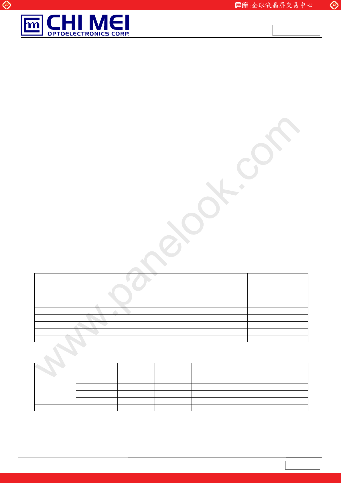
1.4 GENERAL SPECIFICATI0NS
Item Specification Unit Note
Active Area 698.4(H) x 392.85 (V) ( mm
Bezel Opening Area 703.8 (H) x 398.4 (V) mm
Driver Element a-si TFT active matrix -
Pixel Number 1920 x R.G.B. x 1080 pixel
Pixel Pitch (Sub Pixel) 0.12125 (H) x 0.36375 (V) mm
Pixel Arrangement RGB vertical stripe -
Display Colors 1.07G color
Display Operation Mode Transmissive mode / Normally black -
Surface Treatment Glare coating,Hard coating (3H) -
1.5 MECHANICAL SPECIFICATIONS
Item Min. Typ. Max. Unit Note
Horizontal(H) 759 760 761 mm
Vertical(V) 449 450 451 mm
Module Size
Note (1) Please refer to the attached drawings for more information of front and back outline dimensions.
Depth(D) 31.5 32.5 33.5 mm To Rear
Depth(D) 53.2 54.2 55.2 mm To Inverter Cover
Depth(D) 46.5 47.5 48.5 mm To PCB cover
Weight - 5760 - g
4
One step solution for LCD / PDP / OLED panel application: Datasheet, inventory and accessory!
Version1.0
www.panelook.com
Page 5
Global LCD Panel Exchange Center
2. ABSOLUTE MAXIMUM RATINGS
2.1 ABSOLUTE RATINGS OF ENVIRONMENT
Item Symbol
Storage Temperature TST -20 +60 ºC (1)
Operating Ambient Temperature TOP 0 +50 ºC (1), (2)
Shock (Non-Operating) S
Vibration (Non-Operating) V
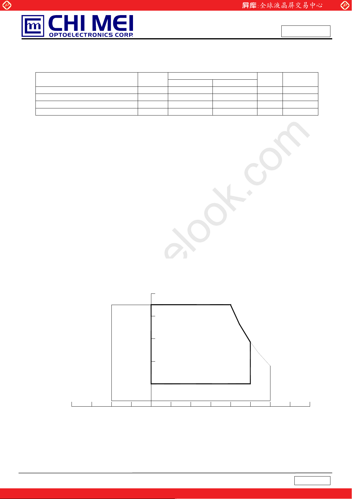
Note (1) Temperature and relative humidity range is shown in the figure below.
(a) 90 %RH Max. (Ta 40 ºC).
(b) Wet-bulb temperature should be 39 ºC Max. (Ta > 40 ºC).
(c) No condensation.
Note (2) The maximum operating temperature is based on the test condition that the surface temperature of
display area is less than or equal to 65 ºC with LCD module alone in a temperature controlled chamber.
www.panelook.com
Issued Date: Sep. 30 ,2009
Model No.: V315H1 – LH3
Preliminary
Value
Min. Max.
- 50 G (3), (5)
NOP
- 1.0 G (4), (5)
NOP
Unit Note
Thermal management should be considered in final product design to prevent the surface temperature of
display area from being over 65 ºC. The range of operating temperature may degrade in case of improper
thermal management in final product design.
Note (3) 11 ms, half sine wave, 1 time for ± X, ± Y, ± Z.
Note (4) 10 ~ 200 Hz, 10 min, 1 time each X, Y, Z.
Note (5) At testing Vibration and Shock, the fixture in holding the module has to be hard and rigid enough so
that the module would not be twisted or bent by the fixture.
Relative Humidity (%RH)
100
90
80
60
Operating Range
40
20
10
Storage Range
Temperature (ºC)
5
One step solution for LCD / PDP / OLED panel application: Datasheet, inventory and accessory!
80 60 -20 40 0 20 -40
Version1.0
www.panelook.com
Page 6
Global LCD Panel Exchange Center
2.2 Package storage
When storing modules as spares for a long time, the following precaution is necessary.
(a) Do not leave the module in high temperature, and high humidity for a long time. It is highly recommended to
store the module with temperature from 0 to 35 at normal humidity without condensation.
(b)The module shall be stored in dark place. Do not store the TFT-LCD module in direct sunlight or
fluorescent light.
2.3 ELECTRICAL ABSOLUTE RATINGS
2.3.1 TFT LCD MODULE
Item Symbol
Power Supply Voltage Vcc -0.3 13.5 V
Input Signal Voltage VIN -0.3 3.6 V
www.panelook.com
Value
Min. Max.
Issued Date: Sep. 30 ,2009
Model No.: V315H1 – LH3
Preliminary
Unit Note
2.3.2 BACKLIGHT UNIT
稊
Value
3000 V
Unit Note
RMS
Item Symbol
Lamp Voltage V
Power Supply Voltage VBL 0 30 V (1)
Control Signal Level
Note (1) Permanent damage to the device may occur if maximum values are exceeded. Functional operation
should be restricted to the conditions described under normal operating conditions.
Note (2) No moisture condensation or freezing.
Note (3) The control signals includes Backlight On/Off Control, I_PWM Control, E_PWM Control and ERR
signal for inverter status output.
W
稊
Min. Max.
-0.3 7 V (1), (3)
6
One step solution for LCD / PDP / OLED panel application: Datasheet, inventory and accessory!
Version1.0
www.panelook.com
Page 7
Global LCD Panel Exchange Center
3. ELECTRICAL CHARACTERISTICS
www.panelook.com
Issued Date: Sep. 30 ,2009
Model No.: V315H1 – LH3
Preliminary
3.1 TFT LCD MODULE
Parameter Symbol
Ta = 25 ± 2 ºC
Value
Min. Typ. Max.
Unit Note
Power Supply Voltage VCC 10.8 12.0 13.2 V (1)
Power Supply Ripple Voltage VRP - - 350 mV
Rush Current I
- - 4 A (2)
RUSH
White - 1.5 2 A
Power Supply Current
Common Input Voltage V
interface
Terminating Resistor R
Black - 1.2 A
Vertical Stripe
I
CC
- 1.5 A
1.125 1.25 1.375 V LVDS
LVC
- 100 - ohm
T
(3)
Input High Threshold Voltage VIH 2.7 - 3.3 V CMOS
interface
Input Low Threshold Voltage V
0 - 0.7 V
IL
Note (1) The module should be always operated within above ranges.
Note (2) Measurement Conditions:
+12.0V
R1
1K
Q1 Si4435DY
FUSE
C3
1uF
Vcc
(LCD Module Input)
(Low to High)
(Control Signal)
SW
VR1
47K
R2
1K
Q2
2N7002
Vcc rising time is 470us
0.9Vcc
0.1Vcc
C1
0.01uF
+12V
GND
470us
7
One step solution for LCD / PDP / OLED panel application: Datasheet, inventory and accessory!
Version1.0
www.panelook.com
Page 8
Global LCD Panel Exchange Center
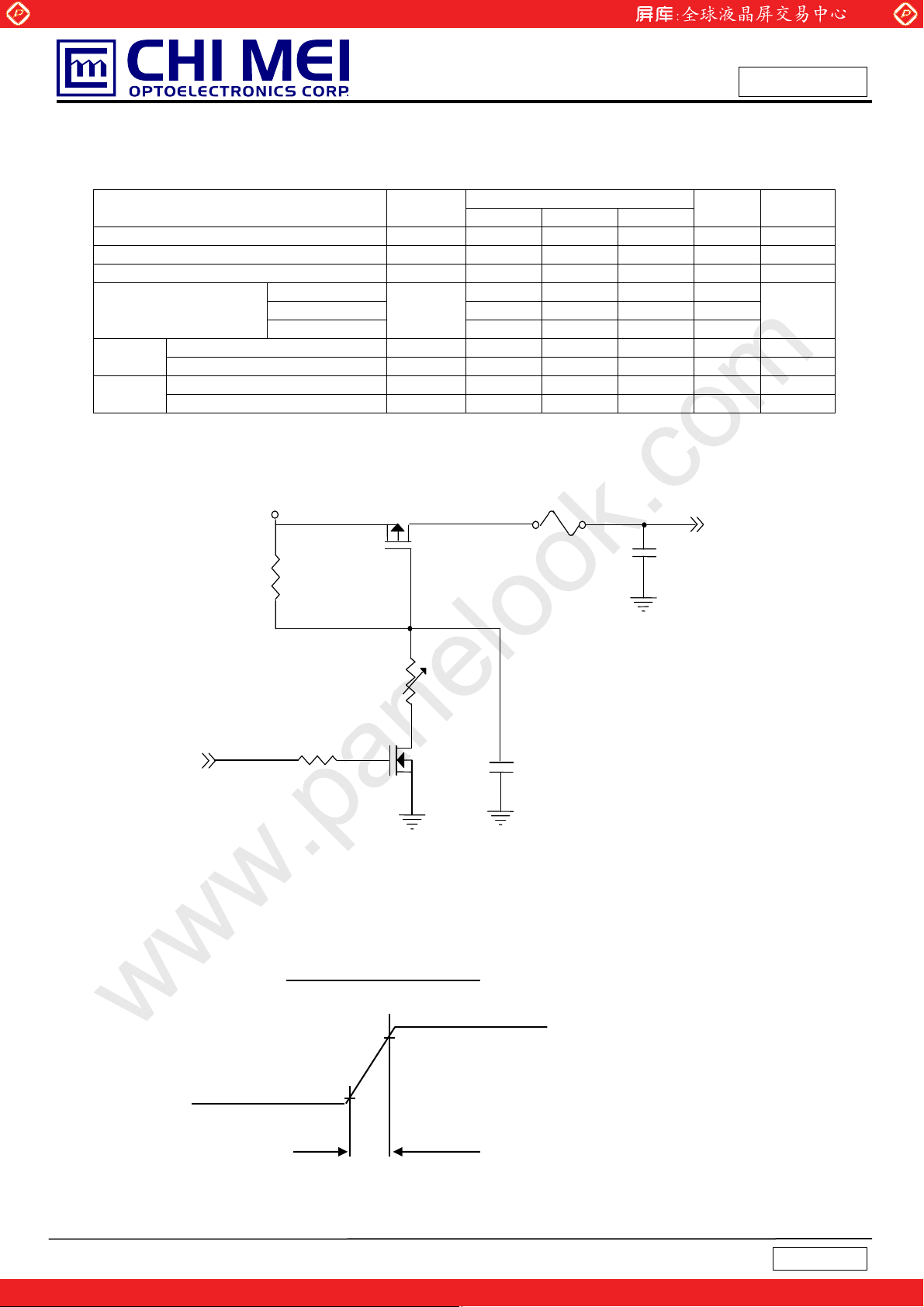
Note (3) The specified power supply current is under the conditions at Vcc =12V, Ta = 25 ± 2 ºC, fv = 60 Hz,
whereas a power dissipation check pattern below is displayed.
www.panelook.com
Issued Date: Sep. 30 ,2009
Model No.: V315H1 – LH3
Preliminary
a. White Pattern
Active Area
c. Vertical Stripe Pattern
b. Black Pattern
Active Area
R
G
R
B
G
B
B
R
R
G
G
B
B
R
Active Area
R
B
R R
G
G
B
B
R
G
G
B
B
R
3.2 BACKLIGHT INVERTER UNIT
3.2.1 CCFL (Cold Cathode Fluorescent Lamp) CHARACTERISTICS (
Parameter Symbol
Lamp Voltage V
Lamp Current I
Lamp Starting Voltage V
Operating Frequency FO 40 - 80 KHz
Lamp Life Time LBL 50,000 - Hrs (4)
W
L
S
Min. Typ. Max.
-
11.8 12.3 12.8
- -
- -
Value
2760
2300
Ta = 25 ± 2 ºC)
-
Unit Note
I
V
RMS
mA
RMS
V
RMS
V
RMS
= 12.3mA
L
(2), Ta = 0 ºC
(2), Ta = 25 ºC
8
One step solution for LCD / PDP / OLED panel application: Datasheet, inventory and accessory!
Version1.0
www.panelook.com
Page 9
Global LCD Panel Exchange Center
A
r
www.panelook.com
Issued Date: Sep. 30 ,2009
Model No.: V315H1 – LH3
Preliminary
3.2.2 INVERTER CHARACTERISTICS (
Parameter Symbol
Ta = 25 ± 2 ºC)
Value
Min. Typ. Max.
Unit Note
Power Consumption PBL - 79 81 W (5),(6), IL = 12.3mA
Input Voltage VBL 22.8 24 25.2 V
Input Current I
BL
-
3.29
3.38
Input Ripple Noise - - - 912 mV
DC
P-P
Non Dimming
VBL=22.8V
Oscillating Frequency FW 60 63 66 kHz (3)
Dimming frequency FB 150 160 170 Hz
Minimum Duty Ratio D
MIN
- 20 - %
Note (1) Lamp current is measured by utilizing AC current probe and its value is average by measuring
master and slave board.
Note (2) The lamp starting voltage V
should be applied to the lamp for more than 1 second after startup.
S
Otherwise the lamp may not be turned on.
Note (3) The lamp frequency may produce interference with horizontal synchronous frequency of the
display input signals, and it may result in line flow on the display. In order to avoid interference, the
lamp frequency should be detached from the horizontal synchronous frequency and its harmonics
as far as possible.
Note (4) The life time of a lamp is defined as when the brightness is larger than 50% of its original value and
the effective discharge length is longer than 80% of its original length (Effective discharge length is
defined as an area that has equal to or more than 70% brightness compared to the brightness at the
center point of lamp.) as the time in which it continues to operate under the condition at Ta = 25 2
and I
= 11.8~ 12.8mArms.
L
Note (5) The power supply capacity should be higher than the total inverter power consumption P
the pulse width modulation (PWM) mode was applied for backlight dimming, the driving current
changed as PWM duty on and off. The transient response of power supply should be considered for
the changing loading when inverter dimming.
Note (6) The measurement condition of Max. value is based on 31.5" backlight unit under input voltage 24V,
average lamp current 12.6 mA and lighting 30 minutes later.
LCD
Module
A
A
A
A
A
A
A
A
HV (Pink)
HV (White)
HV (Pink)
HV (White)
HV (Pink)
HV (White)
HV (Pink)
HV (White)
1
2
1
2
1
Inverte
2
1
2
. Since
BL
9
One step solution for LCD / PDP / OLED panel application: Datasheet, inventory and accessory!
Version1.0
www.panelook.com
Page 10
Global LCD Panel Exchange Center
A
www.panelook.com
3.2.3 INVERTER INTERFACE CHARACTERISTICS
Parameter Symbol
On/Off Control Voltage
Internal PWM Control
Voltage
Voltage
Error Signal
ON
OFF
MAX 2.85 3.0 3.15 V Maximum duty ratio
MIN
HI 2.0
LO
HI 2.0 5.0 V
LO
V
V
V
ERR
BLON
IPWM
EPWM
VBL Rising Time Tr1 稊 30 稊稊 ms
VBL Falling Time Tf1 稊 30 稊稊 ms
Control Signal Rising Time Tr
Control Signal Falling Time Tf
PWM Signal Rising Time T
PWM Signal Falling Time T
PWMR
PWMF
Input impedance R
PWM Delay Time T
BLON Delay Time
PWM
T
T
on1
BLON Off Time T
Condition
IN
on
off
Issued Date: Sep. 30 ,2009
Model No.: V315H1 – LH3
0
稊
0
0
1
Value
稊
稊
0
稊
稊
稊
5.0 V
0.8 V
稊
5.0 V Duty on External PWM Control
0.8 V Duty off
0.8 V Normal
100 ms
100 ms
50 us
50 us
稊稊
Unit Note
V Minimum duty ratio
M˖
Te st
Min. Typ. Max.
稊
2.0
稊
稊
稊
稊
稊稊稊
稊稊稊
稊稊稊
稊稊稊
稊
稊 100 稊 ms
稊 300 稊稊 ms
稊
稊 300 稊稊稊稊 稊 ms
稊稊
稊 300 稊稊 ms
Preliminary
bnormal
10%-90%V
BL
Note (1) The Dimming signal should be valid before backlight turns on by BLON signal. It is inhibited to
change the internal/external PWM signal during backlight turn on period.
Note (2) The power sequence and control signal timing are shown in the following figure. For a certain
reason, the inverter has a possibility to be damaged with wrong power sequence and control
signal timing.
Note (3) While system is turned ON or OFF, the power sequences must follow as below descriptions:
Turn ON sequence: VBL PWM signal BLON
Turn OFF sequence: BLOFF PWM signal VBL
10
One step solution for LCD / PDP / OLED panel application: Datasheet, inventory and accessory!
Version1.0
www.panelook.com
Page 11
Global LCD Panel Exchange Center
www.panelook.com
Issued Date: Sep. 30 ,2009
Model No.: V315H1 – LH3
Preliminary
V
V
V
BL
V
BLON
EPWM
IPWM
9
Toff
%/
Tf1
9
%/
Tr1
9
%/
9
%/
2.0V
0.8V
Ton
Ton1
0
0
Backlight on duration
Tr
Tf
Ext. Dimming Function
T
PWMR
2.0V
0
0.8V
T
PWM
T
PWMF
Floating
3.15V
0
Floating
Int. Dimming Function
V
W
External
PWM
Period
External
PWM Duty
100%
Minimun
Duty
11
One step solution for LCD / PDP / OLED panel application: Datasheet, inventory and accessory!
Version1.0
www.panelook.com
Page 12

Global LCD Panel Exchange Center
4. BLOCK DIAGRAM
4.1 TFT LCD MODULE
CNF1 : FI-RE41S-HF(JAE)
INPUT CONNECTOR
www.panelook.com
Issued Date: Sep. 30 ,2009
Model No.: V315H1 – LH3
Preliminary
SCAN DRIVER
VBL
GND
ERR
BLON
CN1
CNF2 : FI-RE51S-HF(JAE)
INPUT CONNECTOR
INVERTER CONNECTOR
C
N1:
CviLux CI0114M1HR0-LA
BACKLIGHT
UNIT
I_PWM
E_PWN
12
One step solution for LCD / PDP / OLED panel application: Datasheet, inventory and accessory!
Version1.0
www.panelook.com
Page 13

Global LCD Panel Exchange Center
www.panelook.com
5. INTERFACE PIN CONNECTION
5.1 TFT LCD MODULE
CNF2 Connector Pin Assignment (FI-RE51S-HF(JAE) or equivalent)
Pin Name Description Note
1 GND Ground
2 N.C. No Connection (1)
3 N.C. No Connection (1)
4 N.C. No Connection (1)
5 N.C. No Connection (1)
6 N.C. No Connection (1)
Issued Date: Sep. 30 ,2009
Model No.: V315H1 – LH3
Preliminary
7 SELLVDS LVDS Data Format Selection (2)
8 N.C. No Connection (1)
9 N.C. No Connection (1)
10 N.C. No Connection (1)
11 GND Ground
12 ARX0- First pixel Negative LVDS differential data input. Channel 0
13 ARX0+ First pixel Positive LVDS differential data input. Channel 0
14 ARX1- First pixel Negative LVDS differential data input. Channel 1
15 ARX1+ First pixel Positive LVDS differential data input. Channel 1
16 ARX2- First pixel Negative LVDS differential data input. Channel 2
17 ARX2+ First pixel Positive LVDS differential data input. Channel 2
18 GND Ground
19 ACLK- First pixel Negative LVDS differential clock input.
20 ACLK+ First pixel Positive LVDS differential clock input.
21 GND Ground
22 ARX3- First pixel Negative LVDS differential data input. Channel 3
23 ARX3+ First pixel Positive LVDS differential data input. Channel 3
24 ARX4- First pixel Negative LVDS differential data input. Channel 4
25 ARX4+ First pixel Positive LVDS differential data input. Channel 4
26 N.C. No Connection (1)
27 N.C. No Connection (1)
13
One step solution for LCD / PDP / OLED panel application: Datasheet, inventory and accessory!
Version1.0
www.panelook.com
Page 14

Global LCD Panel Exchange Center
28 BRX0- Second pixel Negative LVDS differential data input. Channel 0
29 BRX0+ Second pixel Positive LVDS differential data input. Channel 0
30 BRX1- Second pixel Negative LVDS differential data input. Channel 1
31 BRX1+ Second pixel Positive LVDS differential data input. Channel 1
32 BRX2- Second pixel Negative LVDS differential data input. Channel 2
33 BRX2+ Second pixel Positive LVDS differential data input. Channel 2
34 GND Ground
35 BCLK- Second pixel Negative LVDS differential clock input.
36 BCLK+ Second pixel Positive LVDS differential clock input.
37 GND Ground
www.panelook.com
Issued Date: Sep. 30 ,2009
Model No.: V315H1 – LH3
Preliminary
38 BRX3- Second pixel Negative LVDS differential data input. Channel 3
39 BRX3+ Second pixel Positive LVDS differential data input. Channel 3
40 BRX4- Second pixel Negative LVDS differential data input. Channel 4
41 BRX4+ Second pixel Positive LVDS differential data input. Channel 4
42 N.C. No Connection (1)
43 N.C. No Connection (1)
44 GND Ground
45 GND Ground
46 GND Ground
47 N.C. No Connection (1)
48 VCC +12V power supply
49 VCC +12V power supply
50 VCC +12V power supply
51 VCC +12V power supply
CNF1 Connector Pin Assignment (FI-RE41S-HF(JAE) or equivalent)
Pin Name Description Note
1 GND Ground
2 N.C. No Connection (1)
3 N.C. No Connection (1)
4 N.C. No Connection (1)
5 N.C. No Connection (1)
14
One step solution for LCD / PDP / OLED panel application: Datasheet, inventory and accessory!
Version1.0
www.panelook.com
Page 15

Global LCD Panel Exchange Center
6 N.C. No Connection (1)
7 N.C. No Connection (1)
8 N.C. No Connection (1)
9 GND Ground
10 CRX0- Third pixel Negative LVDS differential data input. Channel 0
11 CRX0+ Third pixel Positive LVDS differential data input. Channel 0
12 CRX1- Third pixel Negative LVDS differential data input. Channel 1
13 CRX1+ Third pixel Positive LVDS differential data input. Channel 1
14 CRX2- Third pixel Negative LVDS differential data input. Channel 2
15 CRX2+ Third pixel Positive LVDS differential data input. Channel 2
www.panelook.com
Issued Date: Sep. 30 ,2009
Model No.: V315H1 – LH3
Preliminary
16 GND Ground
17 CCLK- Third pixel Negative LVDS differential clock input.
18 CCLK+ Third pixel Positive LVDS differential clock input.
19 GND Ground
20 CRX3- Third pixel Negative LVDS differential data input. Channel 3
21 CRX3+ Third pixel Positive LVDS differential data input. Channel 3
22 CRX4- Third pixel Negative LVDS differential data input. Channel 4
23 CRX4+ Third pixel Positive LVDS differential data input. Channel 4
24 N.C. No Connection (1)
25 N.C. No Connection (1)
26 DRX0- Fourth pixel Negative LVDS differential data input. Channel 0
27 DRX0+ Fourth pixel Positive LVDS differential data input. Channel 0
28 DRX1- Fourth pixel Negative LVDS differential data input. Channel 1
29 DRX1+ Fourth pixel Positive LVDS differential data input. Channel 1
30 DRX2- Fourth pixel Negative LVDS differential data input. Channel 2
31 DRX2+ Fourth pixel Positive LVDS differential data input. Channel 2
32 GND Ground
33 DCLK- Fourth pixel Negative LVDS differential clock input.
34 DCLK+ Fourth pixel Positive LVDS differential clock input.
35 GND Ground
36 DRX3- Fourth pixel Negative LVDS differential data input. Channel 3
15
One step solution for LCD / PDP / OLED panel application: Datasheet, inventory and accessory!
Version1.0
www.panelook.com
Page 16

Global LCD Panel Exchange Center
37 DRX3+ Fourth pixel Positive LVDS differential data input. Channel 3
38 DRX4- Fourth pixel Negative LVDS differential data input. Channel 4
39 DRX4+ Fourth pixel Positive LVDS differential data input. Channel 4
40 N.C. No Connection (1)
41 N.C. No Connection (1)
Note (1) Please be reserved to open.
Note (2) Low or Open: VESA Format (Default), High: JEIDA Format.
Note (3) LVDS 4-port Data Mapping
Port Channel of LVDS Data Stream
1st Port First Pixel 1, 5, 9, ……1913, 1917
www.panelook.com
Issued Date: Sep. 30 ,2009
Model No.: V315H1 – LH3
Preliminary
2nd Port Second Pixel 2, 6, 10, ….1914, 1918
3rd Port Third Pixel 3, 7, 11, ….1915, 1919
4th Port Fourth Pixel 4, 8, 12, ….1916, 1920
16
One step solution for LCD / PDP / OLED panel application: Datasheet, inventory and accessory!
Version1.0
www.panelook.com
Page 17

Global LCD Panel Exchange Center
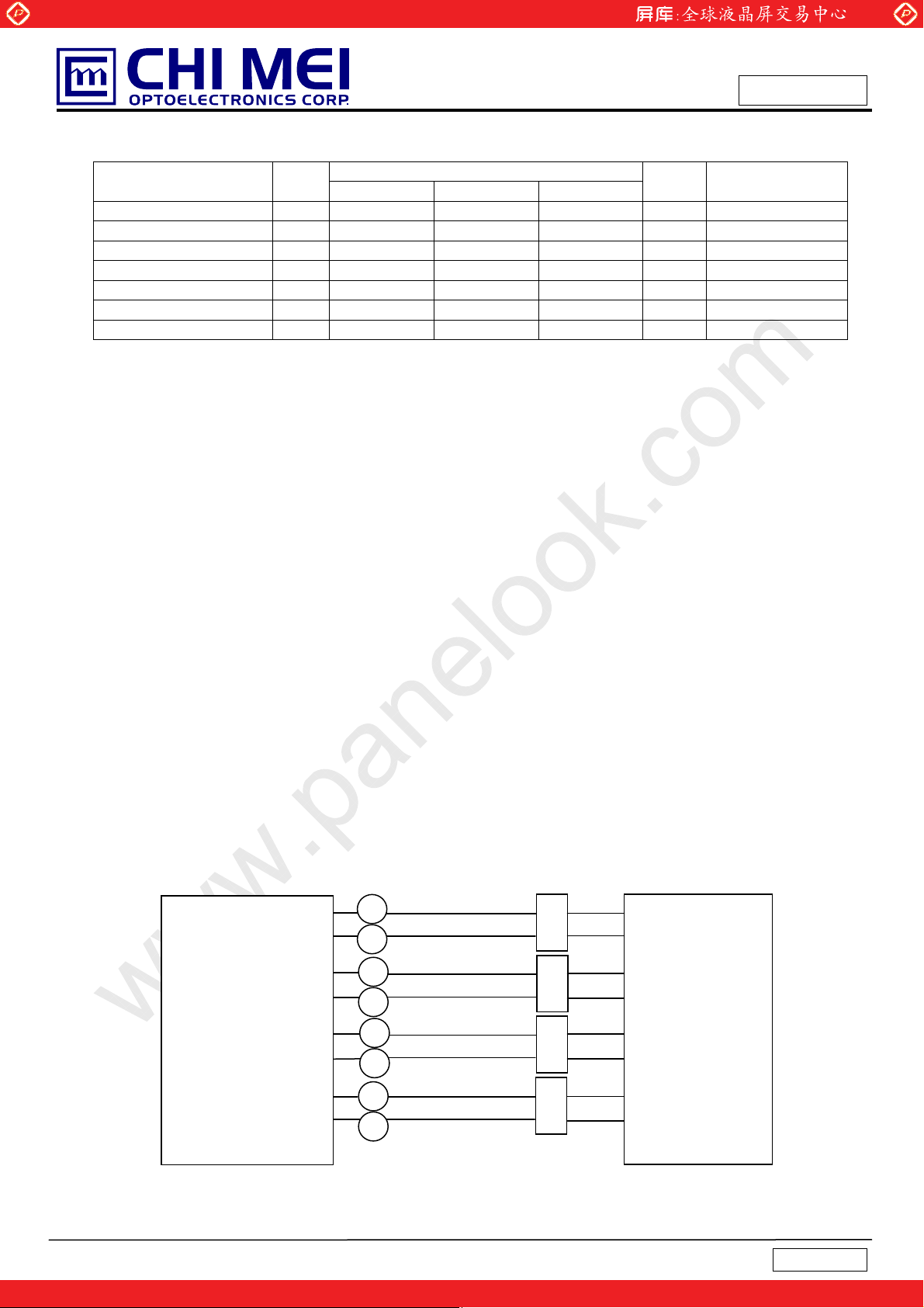
5.2 BACKLIGHT UNIT
The backlight interface for high voltage side is Yeoho 90050GS-32DLQ or JST E08B-KCBSH-450
www.panelook.com
Issued Date: Sep. 30 ,2009
Model No.: V315H1 – LH3
Preliminary
HV, +
HV, -
HV, +
HV, -
HV, +
HV, -
HV, +
HV, -
Yeoho 90050GS-32DLQ or JST E08B-KCBSH-450
17
One step solution for LCD / PDP / OLED panel application: Datasheet, inventory and accessory!
Version1.0
www.panelook.com
Page 18

Global LCD Panel Exchange Center
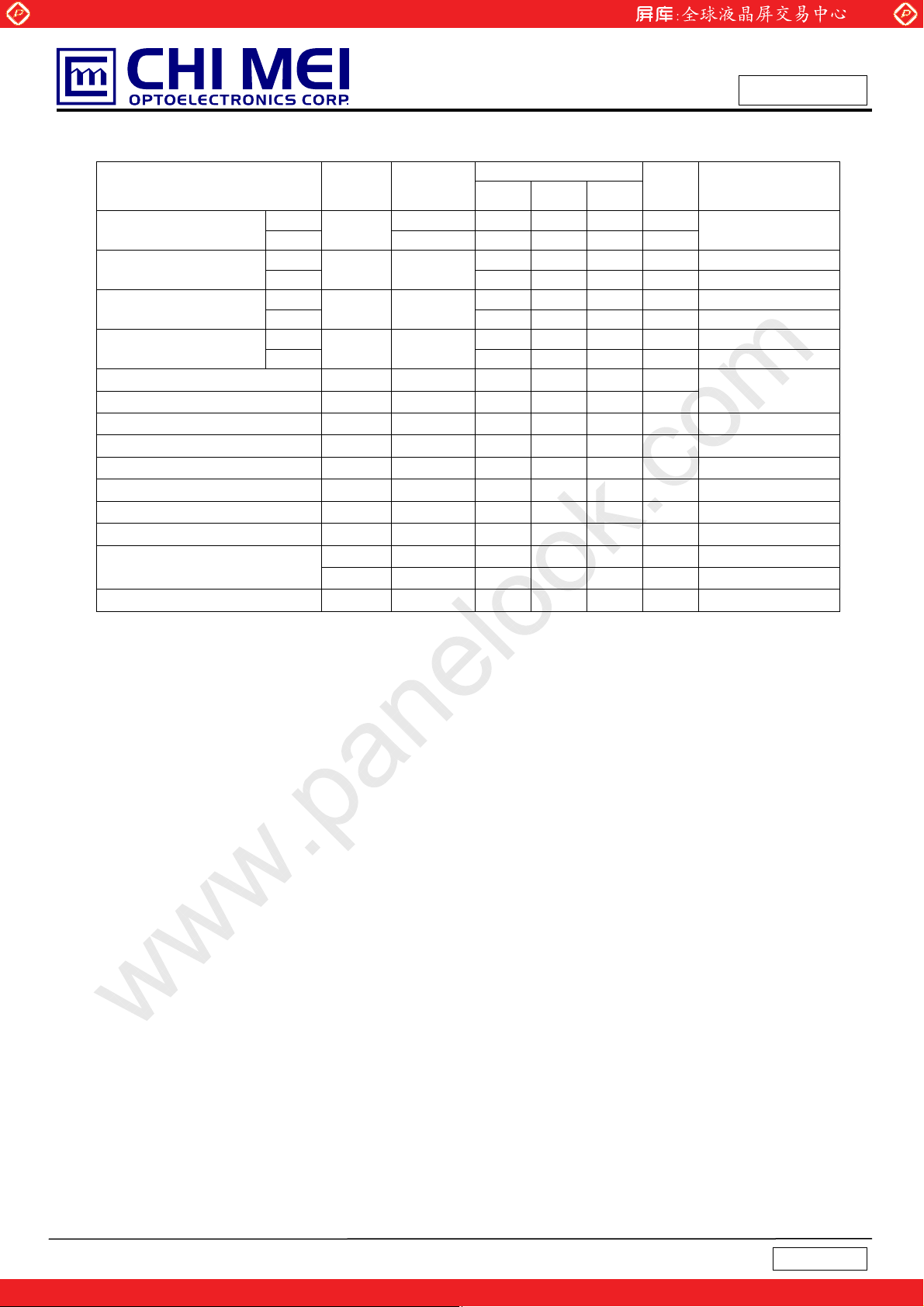
5.3 INVERTER UNIT
www.panelook.com
Issued Date: Sep. 30 ,2009
Model No.: V315H1 – LH3
Preliminary
CN1(Header):
Pin No. Symbol Description
1
2
3
4
5
6
7
8
9
10
11 ERR
12 BLON Backlight on/off control
13 I_PWM Internal PWM control signal
14 E_PWM External PWM control signal
Notice:
#PIN 13: Internal PWM control (Use Pin 13): Pin 14 must open.
#PIN 14: External PWM control (Use Pin 14): Pin 13 must open.
#Pin 13(I_PWM) and Pin 14(E_PWM) can not open in same period.
CviLux CI0114M1HR0-LA
VBL +24V Power input
GND Ground
Normal (GND)
Abnormal ( open collector)
CN2-CN5: CviLux CP042EP1MFB-LF
Pin No. Symbol Description
1
2
CCFL HOT
CCFL HOT
CCFL high voltage
CCFL high voltage
18
One step solution for LCD / PDP / OLED panel application: Datasheet, inventory and accessory!
Version1.0
www.panelook.com
Page 19

Global LCD Panel Exchange Center
5.4 BLOCK DIAGRAM OF INTERFACE
www.panelook.com
Issued Date: Sep. 30 ,2009
Model No.: V315H1 – LH3
Preliminary
19
One step solution for LCD / PDP / OLED panel application: Datasheet, inventory and accessory!
Version1.0
www.panelook.com
Page 20

Global LCD Panel Exchange Center
AR0~AR9: First pixel R data
AG0~AG9: First pixel G data
AB0~AB9: First pixel B data
BR0~BR9: Second pixel R data
BG0~BG9: Second pixel G data
BB0~BB9: Second pixel B data
DE: Data enable signal
DCLK: Data clock signal
The third and fourth pixel are followed the same rules.
CR0~CR9: Third pixel R data
CG0~CG9: Third pixel G data
www.panelook.com
Issued Date: Sep. 30 ,2009
Model No.: V315H1 – LH3
Preliminary
CB0~CB9: Third pixel B data
DR0~DR9: Fourth pixel R data
DG0~DG9: Fourth pixel G data
DB0~DB9: Fourth pixel B data
Note (1) A ~ D channel are first, second, third and fourth pixel respectively.
Note (2) The system must have the transmitter to drive the module.
Note (3) LVDS cable impedance shall be 50 ohms per signal line or about 100 ohms per twist-pair line when it is
used differentially.
20
One step solution for LCD / PDP / OLED panel application: Datasheet, inventory and accessory!
Version1.0
www.panelook.com
Page 21

Global LCD Panel Exchange Center
5.5 LVDS INTERFACE
VESA Format : SELLVDS = L or Open
JEIDA Format : SELLVDS = H
VESA Format
www.panelook.com
Issued Date: Sep. 30 ,2009
Model No.: V315H1 – LH3
Preliminary
Current Cycle
AR 0P
AR 0N
AR 1P
AR 1N
AR 2P
AR 2N
AR 3P
AR 3N
AR 4P
AR 4N
JEIDA Format
AR 0P
AR 0N
AR 1P
AR 1N
AR0
AG1
AB2
AR6
AR4
AG5
AG0 AR5
AB1
DE VS HS AB5 AB4 AB3 AB2
REV AB7 AB6 AG7 AG6 AR7 AR6
REV AB9 AB8 AG9 AG8 AR9 AR8AR8 REV
AG4 AR7
AB5
AB0 AG5 AG4 AG3 AG2 AG1
AB4 AG7 AG6 AG5AG9 AG8
AR4 AR3 AR2 AR1 AR0
AR6 AR5 AR4AR9 AR8
AG0
AB1
DE
REV
AG4
AB5
AR 2P
AR 2N
AR 3P
AR 3N
AR 4P
AR 4N
AR0~AR9: First Pixel R Data (9; MSB, 0; LSB)
AG0~AG9: First Pixel G Data (9; MSB, 0; LSB)
AB0~AB9: First Pixel B Data (9; MSB, 0; LSB)
DE : Data enable signal
DCLK : Data clock signal
RSVD : Reserved
AB6
AR2
DE VS HS AB7 AB6AB9 AB8
REV AB3 AB2 AG3 AG2 AR3 AR2
REV AB1 AB0 AG1 AG0 AR1 AR0AR0 REV
21
One step solution for LCD / PDP / OLED panel application: Datasheet, inventory and accessory!
DE
REV
Version1.0
www.panelook.com
Page 22

Global LCD Panel Exchange Center
5.6 COLOR DATA INPUT ASSIGNMENT
The brightness of each primary color (red, green and blue) is based on the 10-bit gray scale data input for
the color. The higher the binary input, the brighter the color. The table below provides the assignment of color
versus data input.
www.panelook.com
Issued Date: Sep. 30 ,2009
Model No.: V315H1 – LH3
Preliminary
Data Signal
Basic
Colors
Gray
Scale
Of
Red
Color
Black
Red
Green
Blue
Cyan
Magenta
Yellow
White
Red (0) / Dark
Red (1)
Red (2)
:
:
Red (1021)
Red (1022)
Red Green Blue
R9 R8 R7 R6 R5 R4 R3 R2 R1 R0 G9 G8 G7 G6 G5 G4 G3 G2 G1 G0 B9 B8 B7 B6 B5 B4 B3 B2 B1 B0
0
0
0
0
0
0
0
0
0
0
0
0
0
0
0
0
0
0
0
0
0
0
0
0
0
0
0
0
0
1
1
1
1
1
1
1
1
1
1
0
0
0
0
0
0
0
0
0
0
0
0
0
0
0
0
0
0
0
0
0
0
0
0
0
0
0
0
0
1
1
1
1
1
1
1
1
1
1
0
0
0
0
0
0
0
0
0
0
0
0
0
0
0
0
0
0
0
0
0
0
0
0
0
0
0
0
0
1
1
1
1
1
1
1
1
1
0
0
0
0
0
0
0
0
0
0
1
1
1
1
1
1
1
1
1
1
1
1
1
1
1
1
1
1
1
1
1
1
1
1
1
1
1
1
1
0
0
0
0
0
0
0
0
0
0
1
1
1
1
1
1
1
1
1
1
1
1
1
1
1
1
1
1
1
1
1
1
1
1
1
1
1
1
1
0
0
0
0
0
0
0
0
0
1
1
1
1
1
1
1
1
1
1
1
1
1
1
1
1
1
1
1
1
1
1
1
1
1
1
1
1
1
0
0
0
0
0
0
0
0
0
0
0
0
0
0
0
0
0
0
0
0
0
0
0
0
0
0
0
0
0
0
0
0
0
0
0
0
0
0
0
1
0
0
0
0
0
0
0
0
0
0
0
0
0
0
0
0
0
0
0
0
0
1
0
0
0
0
0
0
0
0
0
0
0
0
0
0
:
:
:
:
:
:
:
:
:
:
:
:
:
:
:
:
:
:
:
:
:
:
:
:
:
:
:
:
:
:
:
:
:
:
:
:
:
:
:
;
:
:
1
1
1
1
1
1
1
1
0
1
0
0
0
0
0
0
0
0
0
0
0
0
0
1
1
1
1
1
1
1
1
1
0
0
0
0
0
0
0
0
0
0
0
0
0
0
0
0
0
0
:
:
:
:
:
:
0
0
0
0
0
0
0
0
0
0
0
0
0
:
:
:
:
:
:
0
0
0
0
0
0
0
0
0
1
1
1
0
1
0
0
0
:
:
0
0
Gray
Scale
Of
Green
Gray
Scale
Of
Blue
Red (1023)
Green (0) / Dark
Green (1)
Green (2)
:
:
Green (1021)
Green (1022)
Green (1023)
Blue (0) / Dark
Blue (1)
Blue (2)
:
:
Blue (1021)
0
0
0
0
0
0
1
1
1
1
1
1
1
1
1
1
0
0
0
0
0
0
0
0
0
0
0
0
0
0
0
0
0
0
0
0
0
0
0
0
0
0
0
0
0
0
0
0
0
0
0
0
0
0
0
0
0
0
0
0
0
1
0
0
0
0
0
0
0
0
0
0
0
0
0
0
0
0
0
0
0
0
0
1
0
0
0
0
0
0
0
0
0
0
0
0
0
0
:
:
:
:
:
:
:
:
:
:
:
:
:
:
:
:
:
:
:
:
:
:
:
:
:
:
:
:
:
:
0
0
0
0
0
0
0
0
0
0
1
1
0
0
0
0
0
0
0
0
0
0
1
1
0
0
0
0
0
0
0
0
0
0
1
1
0
0
0
0
0
0
0
0
0
0
0
0
0
0
0
0
0
0
0
0
0
0
0
0
0
0
0
0
0
0
0
0
0
0
0
0
:
:
:
:
:
:
:
:
:
:
:
:
:
:
:
:
:
:
:
:
:
:
:
:
0
0
0
0
0
0
0
0
0
0
0
0
:
:
1
1
1
1
1
1
1
1
1
0
0
0
0
0
0
0
0
0
:
:
:
:
:
:
0
0
0
:
:
:
:
1
1
1
1
1
1
1
1
1
0
0
0
0
0
0
0
0
0
:
:
:
:
:
:
0
0
0
0
:
:
:
:
:
:
0
1
0
1
0
0
1
1
0
0
0
0
0
0
0
0
0
0
:
:
:
:
:
:
0
0
1
0
0
0
0
:
:
:
:
:
:
0
0
0
0
0
0
0
0
0
0
0
0
0
0
0
0
0
0
:
:
:
:
:
:
1
1
1
0
0
0
0
0
0
0
:
:
:
:
:
:
0
0
0
0
0
0
0
0
0
0
0
0
0
0
0
0
0
0
:
:
:
:
:
:
1
1
1
0
0
0
0
0
0
0
0
0
0
:
:
:
:
:
:
0
0
0
0
0
0
0
0
0
0
0
0
0
0
1
0
1
0
:
:
:
:
:
:
1
0
1
22
One step solution for LCD / PDP / OLED panel application: Datasheet, inventory and accessory!
Version1.0
www.panelook.com
Page 23

Global LCD Panel Exchange Center
g
r
r
y
y
Blue (1022)
Blue (1023) 000000000000000000000000000000000000000011111111111111111101
Note (1) 0: Low Level Voltage, 1: High Level Voltage
www.panelook.com
6. INTERFACE TIMING
6.1 INPUT SIGNAL TIMING SPECIFICATIONS
The input signal timing specifications are shown as the following table and timing diagram.
Si
nal Item Symbol Min. Typ. Max. Unit Note
Frequency 1/Tc 60 74.25 80 MH
LVDS Receiver Clock
Input cycle to
cycle jitter
Issued Date: Sep. 30 ,2009
Model No.: V315H1 – LH3
Preliminary
Z
Trcl - - 200 ps (1)
(1)
LVDS Receiver Data
Vertical Active Display Term
Horizontal Active Display Term
Note (1) Since this module is operated in DE only mode, Hsync and Vsync input signals should be set to low
logic level. Otherwise, this module would operate abnormally.
(2) Please refer to 5.1 for detail information.
Setup Time Tlvsu 600 - - ps
Hold Time Tlvhd 600 - - ps
F
Frame Rate
Total Tv 1115 1125 1135 Th Tv=Tvd+Tvb
Displa
Blank Tvb 35 45 55 Th Total Th 525 550 575 Tc Th=Thd+Thb
Displa
Blank Thb 45 70 95 Tc -
5
6
F
Tvd 1080 1080 1080 Th -
Thd 480 480 480 Tc -
120
100
Hz
Hz
(1)
(1)
(2)
23
One step solution for LCD / PDP / OLED panel application: Datasheet, inventory and accessory!
Version1.0
www.panelook.com
Page 24

Global LCD Panel Exchange Center
www.panelook.com
Issued Date: Sep. 30 ,2009
Model No.: V315H1 – LH3
Preliminary
INPUT SIGNAL TIMING DIAGRAM
Tv
DE
DCLK
DE
DATA
Th
Tvd
Tc
Thb
Valid display data (1366 clocks)
LVDS RECEIVER INTERFACE TIMING DIAGRAM
Thd
Tvb
RXCLK+/-
RXn+/-
Tlvsu
Tlvhd
1T
14
3T
14
5T
14
Tc
7T
14
24
9T
14
11T
14
13T
14
One step solution for LCD / PDP / OLED panel application: Datasheet, inventory and accessory!
Version1.0
www.panelook.com
Page 25

Global LCD Panel Exchange Center
6.2 POWER ON/OFF SEQUENCE
(Ta = 25 ± 2 ºC)
To prevent a latch-up or DC operation of LCD module, the power on/off sequence should be
as the diagram below.
0V
0.5 T110ms
2
3
50ms
50ms
4
0 T
0 T
500ms T
www.panelook.com
0.1V
CC
T
1
T
2
Issued Date: Sep. 30 ,2009
Model No.: V315H1 – LH3
Preliminary
0.1V
cc
T
3
T
4
LVDS Signals
0 T7T2
0 T
0V
8
T3
Option Signals
(SELLVDS)
Backlight (Recommended)
500ms T
100ms T6
5
Power On
T
7
T
5
Power ON/OFF Sequence
VA L I D
50%
50%
Power Off
T
8
T
6
Note (1):The supply voltage of the external system for the module input should follow the definition of Vcc.
Note (2):Apply the lamp voltage within the LCD operation range. When the backlight turns on before the LCD
operation or the LCD turns off before the backlight turns off, the display may momentarily become
abnormal screen.
Note(3):In case of Vcc is in off level, please keep the level of input signals on the low or high impedance. If
T2<0,that maybe cause electrical overstress failure.
Note (4):T4 should be measured after the module has been fully discharged between power off and on period.
Note (5): Interface signal shall not be kept at high impedance when the power is on.
25
One step solution for LCD / PDP / OLED panel application: Datasheet, inventory and accessory!
Version1.0
www.panelook.com
Page 26

Global LCD Panel Exchange Center
y
(2)
(4)
(5)
y
y
y
y
7. OPTICAL CHARACTERISTICS
7.1 TEST CONDITIONS
Item Symbol Value Unit
Ambient Temperature Ta
Ambient Humidity Ha
Supply Voltage V
Input Signal According to typical value in "3. ELECTRICAL CHARACTERISTICS"
Lamp Current I
Oscillating Frequency (Inverter) F
Frame rate Fr 60 Hz
7.2 OPTICAL SPECIFICATIONS
The relative measurement methods of optical characteristics are shown in 7.2. The following items should
www.panelook.com
CC
L
W
12.3 ± 0.5
Issued Date: Sep. 30 ,2009
Model No.: V315H1 – LH3
Preliminary
o
25±2
50±10
5.0 V
63±3
C
%RH
mA
KHz
be measured under the test conditions described in 7.1 and stable environment shown in Note (6).
Item S
mbol Condition Min. Typ. Max. Unit Note
Contrast Ratio CR 3000 4000 -
Response Time
Center Luminance of White L
White Variation
Cross Talk CT - - 4.0 %
Red
Green
Color
Chromaticity
Blue
White
Color Gamut CG
Viewing
Angle
Horizontal
Vertical
Gray to gray
average
C
δW
=0°, θY =0°
θ
Rx 0.633 R
Gx 0.288 -
x
Viewing Angle at
Normal Direction
G
Bx 0.146 B
4.5 9 ms (3)
360 450 cd/m
- - 1.3 - (7)
0.322 -
Typ
-0.03
0.603 -
Typ
+0.03
0.055 Wx 0.280 W
0.290
-
68 72 % NTSC
θ
+
θ
-
θ
+
θ
-
CR≥20
80 88 80 88 80 88 80 88 -
Deg. (1)
2
(6)
26
One step solution for LCD / PDP / OLED panel application: Datasheet, inventory and accessory!
Version1.0
www.panelook.com
Page 27

Global LCD Panel Exchange Center
Note (1) Definition of Viewing Angle (θx, θy):
Viewing angles are measured by EZ-Contrast 160R (Eldim)
www.panelook.com
Issued Date: Sep. 30 ,2009
Model No.: V315H1 – LH3
Preliminary
Normal
θx = θy = 0º
θy- θy+
θX- = 90º
6 o’clock
θ
y-
= 90º
x-
y-
Note (2) Definition of Contrast Ratio (CR):
The contrast ratio can be calculated by the following expression.
Contrast Ratio (CR) = L1023 / L0
L1023: Luminance of gray level 1023
L 0: Luminance of gray level 0
CR = CR (5), where CR (X) is corresponding to the Contrast Ratio of the point X at the figure in
Note (7).
θx−
θx+
y+
12 o’clock direction
θ
y+
= 90º
x+
θX+ = 90º
Note (3) Definition of Gray to Gray Switching Time :
100%
90%
Optical
Response
10%
0%
Gray to gray
switching time
The driving signal means the signal of luminance 0%, 20%, 40%, 60%, 80%, 100%.
Gray to gray average time means the average switching time of luminance 0%,20%,
40%, 60%, 80%, 100% to each other.
27
Gray to gray
switching time
Time
One step solution for LCD / PDP / OLED panel application: Datasheet, inventory and accessory!
Version1.0
www.panelook.com
Page 28

Global LCD Panel Exchange Center
A
A
www.panelook.com
Issued Date: Sep. 30 ,2009
Model No.: V315H1 – LH3
Preliminary
Note (4) Definition of Luminance of White (LC, L
Measure the luminance of gray level 255 at center point and 5 points
= L (5)
L
C
L
= [L (1)+ L (2)+ L (3)+ L (4)+ L (5)] / 5
AVE
where L (x) is corresponding to the luminance of the point X at the figure in Note (7).
Note (5) Definition of Cross Talk (CT):
CT = | Y
– YA | / YA× 100 (%)
B
Where:
(a)
Y
= Luminance of measured location without gray level 0 pattern (cd/m2)
A
Y
= Luminance of measured location with gray level 0 pattern (cd/m2)
B
ctive Area
Gray 512
Y
A, U
Y
A, R
(D,W)
(D/2,W/8)
(7D/8,W/2)
Y
(D/8,W/2)
A, L
Y
(D/2,7W/8)
A, D
(0, 0)
AVE
):
(D/4,W/4)
Y
(D/8,W/2)
B, L
Y
(D/2,7W/8)
B, D
(0, 0)
ctive Area
Gray 0
Gray 0
Gray 512
Y
(D/2,W/8)
B, U
Y
(7D/8,W/2)
B, R
(3D/4,3W/4)
(D,W)
28
One step solution for LCD / PDP / OLED panel application: Datasheet, inventory and accessory!
Version1.0
www.panelook.com
Page 29

Global LCD Panel Exchange Center
LCD Module
LCD Panel
www.panelook.com
Issued Date: Sep. 30 ,2009
Model No.: V315H1 – LH3
Preliminary
Center of the Screen
Note (7) Definition of White Variation (δW):
Measure the luminance of gray level 1023 at 5 points
δW = Maximum [L (1), L (2), L (3), L (4), L (5)] / Minimum [L (1), L (2), L (3), L (4), L (5)]
Display Color Analyzer
(Minolta CA210)
Light Shield Room
(Ambient Luminance < 2 lux)
Horizontal Line
D
W/4
W/2
W
Vertical Line
3W/4
D/4 D/2 3D/4
1 2
5
3 4
Active Area
X
: Test Point
X=1 to 5
29
One step solution for LCD / PDP / OLED panel application: Datasheet, inventory and accessory!
Version1.0
www.panelook.com
Page 30

Global LCD Panel Exchange Center
8. DEFINITION OF LABELS
8.1 CMO MODULE LABEL
The barcode nameplate is pasted on each module as illustration, and its definitions are as following explanation.
CHI MEI
OPTOELECTRONICS
(a) Model Name: V315H1-LH3
V315H1 -LH3 Rev. XX
www.panelook.com
Issued Date: Sep. 30 ,2009
Model No.: V315H1 – LH3
Preliminary
X X X X X X X Y M D L N N N N
(b) Revision: Rev. XX, for example: A0, A1… B1, B2… or C1, C2…etc.
(c) Serial ID: X X
(d) Production Location:XXXX, for example:TAIWAN or CHINA .
Serial ID includes the information as below:
(a) Manufactured Date: Year: 0~9, for 2000~2009
Day: 1~9, A~Y, for 1
X X X X X Y M D L N N N N
Month: 1~9, A~C, for Jan. ~ Dec.
st
to 31st, exclude I ,O, and U.
Serial No.
Product Line
Year, Month, Date
CMO Internal Use
CMO Internal Use
Revision
CMO Internal Use
(b) Revision Code: Cover all the change
(c) Serial No.: Manufacturing sequence of product
(d) Product Line: 1 -> Line1, 2 -> Line 2, …etc.
30
One step solution for LCD / PDP / OLED panel application: Datasheet, inventory and accessory!
Version1.0
www.panelook.com
Page 31

Global LCD Panel Exchange Center
9. PACKAGING
9.1 PACKING SPECIFICATIONS
(1) 5 LCD TV modules / 1 Box
(2) Box dimensions : 834(L) X 380 (W) X 530 (H)
(3) Weight : approximately 38.5Kg (5 modules per box)
9.2 PACKING METHOD
Figures 9-1 and 9-2 are the packing method
LCD TV Module
www.panelook.com
Issued Date: Sep. 30 ,2009
Model No.: V315H1 – LH3
Preliminary
Carton
Anti-static Bag
Cushion
Carton Label
Figure.9-1 packing method
31
One step solution for LCD / PDP / OLED panel application: Datasheet, inventory and accessory!
Version1.0
www.panelook.com
Page 32

Global LCD Panel Exchange Center
www.panelook.com
Issued Date: Sep. 30 ,2009
Model No.: V315H1 – LH3
Preliminary
Sea / Land Transportation
(40ft Container)
Gross: 303kg
Corner Prot ector
PE Sheet
PP Belt
Film
(L1350*50*50mm t=3)
(L1150*W850*140mm)
Air Transportation
Gross: 207kg
Corner Prot ector
PP Belt
Film
(L1150*W850*140mm)
PE Sheet
(L1055*50*50mm t=5)
Sea / Land Transportation
(40ft HQ Container)
Gross: 414kg
PP Belt
Corner Prot ector
Film
Film
(L1150*W850*140mm)
PE Sheet
PE Sheet
(L1055*50*50mm t=5)
Figure.9-2 packing method
32
One step solution for LCD / PDP / OLED panel application: Datasheet, inventory and accessory!
Version1.0
www.panelook.com
Page 33

Global LCD Panel Exchange Center
www.panelook.com
Issued Date: Sep. 30 ,2009
Model No.: V315H1 – LH3
Preliminary
10. PRECAUTIONS
10.1 ASSEMBLY AND HANDLING PRECAUTIONS
(1) Do not apply rough force such as bending or twisting to the module during assembly.
(2) It is recommended to assemble or to install a module into the user’s system in clean working areas. The
dust and oil may cause electrical short or worsen the polarizer.
(3) Do not apply pressure or impulse to the module to prevent the damage of LCD panel and backlight.
(4) Always follow the correct power-on sequence when the LCD module is turned on. This can prevent the
damage and latch-up of the CMOS LSI chips.
(5) Do not plug in or pull out the I/F connector while the module is in operation.
(6) Do not disassemble the module.
(7) Use a soft dry cloth without chemicals for cleaning, because the surface of polarizer is very soft and
easily scratched.
(8) Moisture can easily penetrate into LCD module and may cause the damage during operation.
(9) High temperature or humidity may deteriorate the performance of LCD module. Please store LCD
modules in the specified storage conditions.
(10) When ambient temperature is lower than 10ºC, the display quality might be reduced. For example, the
response time will become slow, and the starting voltage of CCFL will be higher than that of room
temperature.
10.2 SAFETY PRECAUTIONS
(1) The startup voltage of a backlight is over 1000 Volts. It may cause an electrical shock while assembling
with the inverter. Do not disassemble the module or insert anything into the backlight unit.
(2) If the liquid crystal material leaks from the panel, it should be kept away from the eyes or mouth. In case
of contact with hands, skin or clothes, it has to be washed away thoroughly with soap.
(3) After the module’s end of life, it is not harmful in case of normal operation and storage.
10.3 SAFETY STANDARDS
The LCD module should be certified with safety regulations as follows:
Regulatory Item Standard
Information Technology equipment
Audio/Video Apparatus
If the module displays the same pattern for a long period of time, the phenomenon of image sticking may be
occurred.
UL UL 60950-1: 2003
cUL
CB IEC 60950-1:2001
UL
cUL
CB
CAN/CSA C22.2 No.60950-1-03
UL 60065: 2003
CAN/CSA C22.2 No.60065-03
IEC 60065:2001
33
One step solution for LCD / PDP / OLED panel application: Datasheet, inventory and accessory!
Version1.0
www.panelook.com
Page 34

Global LCD Panel Exchange Center
11. MECHANICAL CHARACTERISTICS
www.panelook.com
Issued Date: Sep. 30 ,2009
Model No.: V315H1 – LH3
Preliminary
34
One step solution for LCD / PDP / OLED panel application: Datasheet, inventory and accessory!
Version1.0
www.panelook.com
Page 35

Global LCD Panel Exchange Center
www.panelook.com
Issued Date: Sep. 30 ,2009
Model No.: V315H1 – LH3
Preliminary
35
One step solution for LCD / PDP / OLED panel application: Datasheet, inventory and accessory!
Version1.0
www.panelook.com
Page 36

Global LCD Panel Exchange Center
www.panelook.com
Issued Date: Sep. 30 ,2009
Model No.: V315H1 – LH3
Preliminary
36
One step solution for LCD / PDP / OLED panel application: Datasheet, inventory and accessory!
Version1.0
www.panelook.com
 Loading...